WO2008059577A1 - Light guide and light guide structure - Google Patents

Light guide and light guide structure Download PDF

Info

Publication number
WO2008059577A1
WO2008059577A1 PCT/JP2006/322895 JP2006322895W WO2008059577A1 WO 2008059577 A1 WO2008059577 A1 WO 2008059577A1 JP 2006322895 W JP2006322895 W JP 2006322895W WO 2008059577 A1 WO2008059577 A1 WO 2008059577A1
Authority
WO
WIPO (PCT)
Prior art keywords
optical waveguide
norbornene
waveguide according
layer
polymer
Prior art date
Legal status (The legal status is an assumption and is not a legal conclusion. Google has not performed a legal analysis and makes no representation as to the accuracy of the status listed.)
Ceased
Application number
PCT/JP2006/322895
Other languages
English (en)
French (fr)
Inventor
Koji Choki
Tetsuya Mori
Keizo Takahama
Makoto Fujiwara
Kei Watanabe
Hiroshi Owari
Current Assignee (The listed assignees may be inaccurate. Google has not performed a legal analysis and makes no representation or warranty as to the accuracy of the list.)
Sumitomo Bakelite Co Ltd
Original Assignee
Sumitomo Bakelite Co Ltd
Priority date (The priority date is an assumption and is not a legal conclusion. Google has not performed a legal analysis and makes no representation as to the accuracy of the date listed.)
Filing date
Publication date
Application filed by Sumitomo Bakelite Co Ltd filed Critical Sumitomo Bakelite Co Ltd
Priority to US12/447,355 priority Critical patent/US8200058B2/en
Priority to KR1020097009820A priority patent/KR101096300B1/ko
Priority to EP06832775A priority patent/EP2083293A4/en
Priority to CN2006800564012A priority patent/CN101535852B/zh
Priority to PCT/JP2006/322895 priority patent/WO2008059577A1/ja
Publication of WO2008059577A1 publication Critical patent/WO2008059577A1/ja
Anticipated expiration legal-status Critical
Ceased legal-status Critical Current

Links

Classifications

    • GPHYSICS
    • G02OPTICS
    • G02BOPTICAL ELEMENTS, SYSTEMS OR APPARATUS
    • G02B6/00Light guides; Structural details of arrangements comprising light guides and other optical elements, e.g. couplings
    • G02B6/10Light guides; Structural details of arrangements comprising light guides and other optical elements, e.g. couplings of the optical waveguide type
    • G02B6/12Light guides; Structural details of arrangements comprising light guides and other optical elements, e.g. couplings of the optical waveguide type of the integrated circuit kind
    • G02B6/122Basic optical elements, e.g. light-guiding paths
    • G02B6/1221Basic optical elements, e.g. light-guiding paths made from organic materials
    • GPHYSICS
    • G02OPTICS
    • G02BOPTICAL ELEMENTS, SYSTEMS OR APPARATUS
    • G02B6/00Light guides; Structural details of arrangements comprising light guides and other optical elements, e.g. couplings
    • G02B6/10Light guides; Structural details of arrangements comprising light guides and other optical elements, e.g. couplings of the optical waveguide type
    • G02B6/12Light guides; Structural details of arrangements comprising light guides and other optical elements, e.g. couplings of the optical waveguide type of the integrated circuit kind
    • CCHEMISTRY; METALLURGY
    • C08ORGANIC MACROMOLECULAR COMPOUNDS; THEIR PREPARATION OR CHEMICAL WORKING-UP; COMPOSITIONS BASED THEREON
    • C08FMACROMOLECULAR COMPOUNDS OBTAINED BY REACTIONS ONLY INVOLVING CARBON-TO-CARBON UNSATURATED BONDS
    • C08F232/00Copolymers of cyclic compounds containing no unsaturated aliphatic radicals in a side chain, and having one or more carbon-to-carbon double bonds in a carbocyclic ring system
    • C08F232/08Copolymers of cyclic compounds containing no unsaturated aliphatic radicals in a side chain, and having one or more carbon-to-carbon double bonds in a carbocyclic ring system having condensed rings
    • CCHEMISTRY; METALLURGY
    • C08ORGANIC MACROMOLECULAR COMPOUNDS; THEIR PREPARATION OR CHEMICAL WORKING-UP; COMPOSITIONS BASED THEREON
    • C08LCOMPOSITIONS OF MACROMOLECULAR COMPOUNDS
    • C08L51/00Compositions of graft polymers in which the grafted component is obtained by reactions only involving carbon-to-carbon unsaturated bonds; Compositions of derivatives of such polymers
    • C08L51/003Compositions of graft polymers in which the grafted component is obtained by reactions only involving carbon-to-carbon unsaturated bonds; Compositions of derivatives of such polymers grafted on to macromolecular compounds obtained by reactions only involving unsaturated carbon-to-carbon bonds
    • CCHEMISTRY; METALLURGY
    • C08ORGANIC MACROMOLECULAR COMPOUNDS; THEIR PREPARATION OR CHEMICAL WORKING-UP; COMPOSITIONS BASED THEREON
    • C08LCOMPOSITIONS OF MACROMOLECULAR COMPOUNDS
    • C08L53/00Compositions of block copolymers containing at least one sequence of a polymer obtained by reactions only involving carbon-to-carbon unsaturated bonds; Compositions of derivatives of such polymers
    • GPHYSICS
    • G02OPTICS
    • G02BOPTICAL ELEMENTS, SYSTEMS OR APPARATUS
    • G02B1/00Optical elements characterised by the material of which they are made; Optical coatings for optical elements
    • G02B1/04Optical elements characterised by the material of which they are made; Optical coatings for optical elements made of organic materials, e.g. plastics
    • G02B1/045Light guides
    • GPHYSICS
    • G02OPTICS
    • G02BOPTICAL ELEMENTS, SYSTEMS OR APPARATUS
    • G02B6/00Light guides; Structural details of arrangements comprising light guides and other optical elements, e.g. couplings
    • G02B6/10Light guides; Structural details of arrangements comprising light guides and other optical elements, e.g. couplings of the optical waveguide type
    • G02B6/12Light guides; Structural details of arrangements comprising light guides and other optical elements, e.g. couplings of the optical waveguide type of the integrated circuit kind
    • G02B6/13Integrated optical circuits characterised by the manufacturing method
    • G02B6/138Integrated optical circuits characterised by the manufacturing method by using polymerisation
    • GPHYSICS
    • G02OPTICS
    • G02BOPTICAL ELEMENTS, SYSTEMS OR APPARATUS
    • G02B6/00Light guides; Structural details of arrangements comprising light guides and other optical elements, e.g. couplings
    • G02B6/24Coupling light guides
    • G02B6/42Coupling light guides with opto-electronic elements
    • G02B6/43Arrangements comprising a plurality of opto-electronic elements and associated optical interconnections

Definitions

  • the present invention relates to an optical waveguide and an optical waveguide structure.
  • optical communication using optical frequency carrier waves to transfer data has become increasingly important.
  • optical communication there is an optical waveguide as a means for guiding the optical frequency carrier wave to one point force at another point.
  • This optical waveguide is configured to include, for example, a pair of cladding layers and a core layer provided between the pair of cladding layers.
  • the core layer has a linear core part and a clad part, which are arranged alternately.
  • the core part is made of a material that is substantially transparent to light of an optical frequency carrier wave, and the cladding layer and the cladding part are made of a material having a lower refractive index than the core part.
  • the core portion is surrounded by a clad layer and a clad portion having a refractive index lower than that of the core portion. Therefore, the light introduced from the end of the core part is conveyed along the axis of the core part while being reflected at the boundary between the clad layer and the clad part.
  • Examples of the material of the optical waveguide include polymers, etc., in addition to the conventionally used glass. Of these, polymers are promising because they are easy to micro-process and are advantageous for increasing the density of circuit boards in which optical waveguides are incorporated.
  • polymethylmethacrylate see, for example, JP-A-09-258051
  • epoxy resin see, for example, JP-A-2005-070556
  • Fluorinated polyimide see, for example, JP-A No. 4-9807
  • polybenzoxazole see, for example, JP-A No. 2002-173532
  • cellulose acetate petitate Z atelate monomer for example, U.S. Pat. No. 5,292,620
  • polymethylmethacrylate and epoxy resin have a heat resistant temperature of 200 ° C or lower. For this reason, if an optical waveguide composed of these polymers is to be mounted on a circuit board, it may be softened by heat treatment such as soldering.
  • the fluorinated polyimide is a polymer imparted with high heat resistance, high transparency, and low water absorption by fluorination.
  • fluorination is included in the synthesis process, it is expensive and lacks practicality.
  • polymers synthesized by polycondensation such as polybenzoxazole polyimide are cured at a high temperature (250 ° C or higher) to close the imide ring or benzoxazole ring in the polycondensation step. Processing is required. For this reason, there is a problem that workability is poor.
  • the cellulose 'acetate' butyrate z acrylate monomer is softened by a heat treatment such as soldering, which has a heat resistance temperature of 100 ° C or lower.
  • cellulose acetate butyrate has high water absorption because it has many hydroxyl groups. For this reason, when an optical waveguide composed of such a polymer is left in a high humidity environment, a dimensional change due to water absorption occurs.
  • An object of the present invention is to provide an optical waveguide and an optical waveguide structure that have excellent heat resistance, low water absorption, and low material cost.
  • the optical waveguide of the present invention includes:
  • a core layer comprising a core portion and a cladding portion having a lower refractive index than the core portion
  • An optical waveguide having a cladding layer provided in contact with at least one surface of the core layer and having a refractive index lower than that of the core portion;
  • the clad layer is characterized by comprising a norbornene polymer as a main material.
  • optical waveguide having excellent heat resistance, low water absorption, and low material cost can be obtained.
  • the norbornene-based polymer is preferably an addition polymer.
  • the norbornene-based polymer includes an alkyl norbornene repeating unit.
  • the norbornene-based polymer includes a norbornene repeating unit having a substituent containing a polymerizable group.
  • the norbornene-based polymer is mainly one represented by the following chemical formula 1.
  • R represents an alkyl group having 1 to 10 carbon atoms
  • a represents an integer of 0 to 3
  • b represents 1
  • the norbornene-based polymer is crosslinked with a polymerizable group.
  • the average thickness of the clad layer is 0.1 to 1.5 times the average thickness of the core layer.
  • the core layer is activated by irradiation with actinic radiation with a polymer, a monomer that is compatible with the polymer and has a refractive index different from that of the polymer.
  • the active radiation is selectively irradiated to the layer to thereby activate the active layer.
  • the first substance is activated and the activation temperature of the second substance is changed,
  • the second substance or the second substance whose activation temperature has changed is activated, whichever has a lower activation temperature.
  • the monomer By reacting the monomer with an irradiated region or an unirradiated region of the actinic radiation, causing a difference in refractive index between the irradiated region and the unirradiated region, It is preferable that one of the irradiated region and the non-irradiated region is obtained as the core portion and the other as the cladding portion.
  • the core layer is in the other region.
  • the force is preferably obtained by collecting unreacted monomers.
  • the first substance includes a compound that generates a cation and a weakly coordinated ion upon irradiation with the actinic radiation
  • the second substance It is preferable that the active substance temperature of the substance is changed by the action of the weak coordination ion.
  • the activation temperature of the second substance is lowered by the action of the activated first substance, and the second substance is heated at a temperature higher than the temperature of the heat treatment. Therefore, it is preferable that the light is activated without being irradiated with the actinic radiation.
  • the second substance includes a compound represented by the following formula la.
  • E (R) represents a neutral electron donor ligand of group 15 and E represents the first in the periodic table.
  • R represents a hydrogen atom (or one of its isotopes) or a site containing a hydrocarbon group
  • Q represents from carboxylate, thiocarboxylate and dithiocarboxylate Represents the selected lone ligand.
  • the second substance includes a compound represented by the following formula lb. [(E (R)) Pd (Q) (LB)] [WCA] ⁇ ⁇ ⁇ (lb)
  • E (R) represents a neutral electron donor ligand of group 15 and E represents the first in the periodic table.
  • R represents a hydrogen atom (or one of its isotopes) or a site containing a hydrocarbon group
  • Q represents from carboxylate
  • LB represents a Lewis base
  • WCA represents a weakly coordinated arone
  • a represents an integer of 1 to 3
  • b represents 0 to 2
  • the sum of a and b is 1 to 3
  • p and r are numbers that balance the charge between the palladium cation and the weakly coordinated ion.
  • p and r each select an integer force of 1 or 2.
  • the core layer is obtained by heat-treating the layer at a second temperature higher than the temperature of the heat-treatment after the heat-treatment. And are preferred.
  • the core layer is subjected to heat treatment at a third temperature higher than the second temperature after the heat treatment at the second temperature. It is preferable that it is obtained.
  • the third temperature is 20 ° C or higher than the second temperature.
  • the monomer includes a crosslinkable monomer.
  • the monomer is preferably a norbornene-based monomer.
  • the monomer mainly includes a norbornene-based monomer, and includes dimethylbis (norbornenemethoxy) silane as the crosslinkable monomer.
  • the polymer has a leaving group capable of leaving at least a part of the molecular structure from the main chain by the action of the activated first substance.
  • the actinic radiation is selectively irradiated to the layer, the It is preferred that the leaving group of the monomer is removed.
  • the first substance includes a compound that generates a cation and a weakly coordinated ion upon irradiation with the active radiation, and the detachability is
  • the group is preferably an acid leaving group that is released by the action of the cation.
  • the core layer has a molecular structure by the action of the substance activated by irradiation of actinic radiation, the main chain and the substance branched from the main chain and activated. Forming a layer containing a polymer having at least a part of the main chain that can be released from the main chain;
  • the substance is activated in the irradiated region irradiated with the actinic radiation, and the leaving group of the polymer is released,
  • the leaving group of the polymer is released,
  • a refractive index difference between the irradiated region and the non-irradiated region of the active radiation one of the irradiated region and the non-irradiated region is obtained as the core portion, and the other is obtained as the cladding portion. It is preferred that
  • the core layer is obtained by performing a heat treatment on the layer after the irradiation with the active radiation.
  • the substance includes a compound that generates force thione and weakly coordinated ion upon irradiation with the active radiation, and the leaving group is It is preferable that the acid leaving group be released by the action of the cation.
  • the acid leaving group has at least one of an —O structure, an —Si—aryl structure, and an O Si structure.
  • the leaving group causes a decrease in the refractive index of the polymer due to the leaving.
  • the leaving group has a Si-diphenyl structure
  • it is at least one of the O Si diphenyl structures! /.
  • the active radiation has a peak wavelength in a range of 200 to 450 nm.
  • the irradiation amount of the active radiation is preferably 0.1 to 9 jZcm.
  • the active radiation is applied to the layer through a mask.
  • the layer further contains an antioxidant.
  • the layer further contains a sensitizer.
  • the polymer is preferably a norbornene-based polymer.
  • the norbornene-based polymer is preferably an addition polymer.
  • the core portion is composed of a first norbornene-based material as a main material, and the cladding portion has a second refractive index lower than that of the first norbornene-based material. It is preferable that the main material is norbornene-based material.
  • the first norbornene-based material and the second norbornene-based material both contain the same norbornene-based polymer, and the norbornene-based polymer It is preferable that the refractive indexes of the norbornene-based monomers having different refractive indexes differ from each other due to the different contents of the reactants.
  • the reactant is a polymer of the norbornene-based monomer, a crosslinked structure that crosslinks the norbornene-based polymers, and a branched structure that also branches the norbornene-based polymer force. At least one of the above is preferable.
  • the norbornene-based polymer includes a repeating unit of aralkyl norbornene.
  • the norbornene-based polymer includes a repeating unit of benzylnorbornene.
  • the norbornene-based polymer preferably includes a repeating unit of ferroethylnorbornene.
  • the norbornene-based polymer includes a main chain and the main chain. Branched, and at least a part of the molecular structure has a leaving group that can be detached from the main chain, and the core part and the clad part are different in the number of the leaving groups bonded to the main chain. It is preferable that the refractive indexes of the norbornene-based monomers having different refractive indexes from those of the norbornene-based polymers are different from each other.
  • the core layer has norbornene having a main chain and a leaving group that is branched from the main chain, and at least a part of the molecular structure can be separated from the main chain. It is composed mainly of a polymer and
  • first norbornene-based material and the second norbornene-based material have different refractive indexes because the number of the leaving groups bonded to the main chain is different.
  • the norbornene-based polymer includes a repeating unit of diphenylmethylnorbornenemethoxysilane.
  • the norbornene-based polymer includes an alkyl norbornene repeating unit.
  • the norbornene-based polymer includes a repeating unit of hexylnorbornene.
  • the norbornene-based polymer is preferably an addition polymer.
  • the optical waveguide structure of the present invention comprises:
  • It has the above-mentioned optical waveguide and a conductor layer provided on at least one surface side of the optical waveguide.
  • the average thickness of the conductor layer is preferably 10 to 90% of the average thickness of the optical waveguide.
  • the conductor layer is formed by at least one of a dry plating method, a wet plating method, and a joining of conductive sheet materials. It is preferable.
  • FIG. 1 is a perspective view (partially cut away) showing an embodiment of an optical waveguide structure of the present invention.
  • FIG. 2 is a cross-sectional view schematically showing a process example of the first manufacturing method of the optical waveguide structure of the present invention.
  • FIG. 3 is a cross-sectional view schematically showing a process example of the first manufacturing method of the optical waveguide structure of the present invention.
  • FIG. 4 is a cross-sectional view schematically showing a process example of the first manufacturing method of the optical waveguide structure of the present invention.
  • FIG. 5 is a cross-sectional view schematically showing a process example of the first manufacturing method of the optical waveguide structure of the present invention.
  • FIG. 6 is a cross-sectional view schematically showing a process example of the first manufacturing method of the optical waveguide structure of the present invention.
  • FIG. 7 is a cross-sectional view schematically showing a process example of the first manufacturing method of the optical waveguide structure of the present invention.
  • FIG. 8 is a cross-sectional view schematically showing a process example of the fourth manufacturing method of the optical waveguide structure of the present invention.
  • FIG. 9 is a cross-sectional view schematically showing a process example of the fourth manufacturing method of the optical waveguide structure of the present invention.
  • FIG. 10 is a cross-sectional view schematically showing a process example of the fourth manufacturing method of the optical waveguide structure of the present invention.
  • FIG. 11 is a cross-sectional view schematically showing a process example of the fourth manufacturing method of the optical waveguide structure of the present invention.
  • FIG. 12 is a cross-sectional view schematically showing a process example of the fourth manufacturing method of the optical waveguide structure of the present invention.
  • FIG. 13 is a cross-sectional view schematically showing a process example of the fourth manufacturing method of the optical waveguide structure of the present invention.
  • FIG. 14 is a chart showing changes in total optical loss accompanying changes in the length of the core part.
  • FIG. 1 is a perspective view (partially cut away) showing an embodiment of an optical waveguide structure of the present invention.
  • the upper side in FIG. 1 is “upper” or “upper”, and the lower side is “lower” or “lower” (the same applies to the following figures).
  • An optical waveguide structure 9 shown in FIG. 1 has an optical waveguide 90 and conductor layers 901 and 902 provided on the upper surface and the lower surface, respectively, and these layers are bonded to each other. .
  • Constituent materials of the conductor layers 901 and 902 are, for example, various metal materials such as copper, copper-based alloy, aluminum, and aluminum-based alloy, indium stannate (ITO), fluorine, and the like. Examples include various oxide materials such as silicon-containing indium stannate (FTO).
  • the average thickness of the conductor layers 901 and 902 is preferably about 10 to 90% of the average thickness of the optical waveguide 90, more preferably about 20 to 80%.
  • the average thicknesses of the conductor layers 901 and 902 are not particularly limited, but are usually preferably about 5 to 70; ⁇ ⁇ is preferably about 3 to about LOO / zm.
  • the conductor layers 901 and 902 can be made excellent in conductivity while preventing the flexibility of the optical waveguide structure 9 from being lowered.
  • the conductor layers 901 and 902 both have a flat plate shape (sheet shape).
  • an optical element (light-emitting element, light-receiving element, etc.) is mounted at a desired location, thereby providing a composite device comprising an optical circuit and an electric circuit. Can be manufactured.
  • Each of the conductor layers 901 and 902 may be previously patterned (wiring). Further, if necessary, one of the conductor layers 901 and 902 may be omitted.
  • the conductor layers 901 and 902 and the optical waveguide 90 there is an arbitrary purpose (for example, adhesion). There may be one or more layers for the purpose of improvement).
  • the optical waveguide 90 is formed by laminating a cladding layer (lower cladding layer) 91, a core layer 93, and a cladding layer (upper cladding layer) 92 in this order from the lower side in FIG.
  • a core part 94 having a predetermined pattern and a clad part 95 adjacent to the core part (waveguide channel) 94 are formed in 93.
  • the difference in refractive index between the core portion 94 and the clad portion 95 is not particularly limited, but is preferably about 0.3 to 5.5%, and particularly preferably about 0.8 to 2.2%. If the difference in refractive index is less than the lower limit, the effect of transmitting light may be reduced, and even if the upper limit is exceeded, no further increase in the light transmission efficiency can be expected! /.
  • the refractive index difference is expressed by the following equation, where A is the refractive index of the core portion 94 and B is the refractive index of the cladding portion 95.
  • Refractive index difference (%) I A / B- 1 I X 100
  • the core portion 94 may have any shape that may be curved, branched, or the like in the course of a force that is linearly formed in plan view. If a method for manufacturing the optical waveguide structure 9 as described later is used, the core portion 94 having a complicated and arbitrary shape can be easily formed with high dimensional accuracy.
  • the core section 94 has a quadrangular shape such as a square or a rectangle (rectangle) in cross section.
  • the width and height of the core portion 94 are not particularly limited, but are preferably about 1 to 200 ⁇ m, respectively. 5 to about 10 to 60, more preferably about LOO m. More preferably, it is about m.
  • the core portion 94 is made of a material having a higher refractive index than that of the cladding portion 95, and is also made of a material having a higher refractive index than the cladding layers 91 and 92.
  • the clad layers 91 and 92 constitute the clad portions located at the lower part and the upper part of the core part 94, respectively.
  • the core portion 94 functions as a light guide path whose outer periphery is surrounded by the clad portion.
  • the average thickness of the cladding layers 91 and 92 is preferably about 0.1 to 1.5 times the average thickness of the core layer 93, and is about 0.3 to 1.25 times. Specifically, the cladding layer 91 is more preferable.
  • the average thickness of 92 is not particularly limited, but is preferably about 1 to 200 / ⁇ ⁇ , respectively. 5 to about 10 to 60 / ⁇ is more preferably about LOO m. More preferably, it is about ⁇ .
  • the function as the cladding layer is suitably exhibited while preventing the optical waveguide 90 from becoming unnecessarily large (pressure film).
  • the constituent materials of the clad layer 91, the clad portion 95, and the clad layer 92 may be the same (same type) or different, but they have the same or similar refractive index. It is preferable. Details of the constituent materials of the cladding layers 91 and 92 and the core layer 93 will be described later.
  • the optical waveguide structure 9 of the present invention is slightly different depending on the optical characteristics of the material of the core portion 94 and is not particularly limited.
  • the optical waveguide structure 9 is suitable for data communication using light in the wavelength region of about 600 to 1550 nm. Therefore, it is preferably used.
  • FIGS 2 to 7 are cross-sectional views schematically showing process examples of the first manufacturing method of the optical waveguide structure of the present invention.
  • a layer 910 is formed on a support substrate 951 (see FIG. 2).
  • the layer 910 is formed by a method in which a core layer forming material (varnish) 900 is applied and cured (solidified).
  • the layer 910 is formed by applying the core layer forming material 900 on the support substrate 951 to form a liquid film, and then placing the support substrate 951 on a ventilated level table, It is formed by leveling uneven surfaces and evaporating (desolving) the solvent.
  • the layer 910 is formed by a coating method, for example, a method such as a doctor blade method, a spin coating method, a detting method, a table coating method, a spray method, an applicator method, a curtain coating method, a die coating method, etc.
  • a coating method for example, a method such as a doctor blade method, a spin coating method, a detting method, a table coating method, a spray method, an applicator method, a curtain coating method, a die coating method, etc.
  • a coating method for example, a method such as a doctor blade method, a spin coating method, a detting method, a table coating method, a spray method, an applicator method, a curtain coating method, a die coating method, etc.
  • the support substrate 95 for example, a silicon substrate, a silicon dioxide substrate, a glass substrate, a quartz substrate, a polyethylene terephthalate (PET) film, or the like is used.
  • the core layer forming material 900 is a photo-induced heat-developable material composed of a polymer 915 and an additive 920 (in this embodiment, including at least a monomer, a promoter, and a catalyst precursor).
  • PITDM a material in which a monomer reaction occurs in polymer 915 upon irradiation with actinic radiation and heating.
  • the average thickness of such a layer 910 is appropriately set according to the thickness of the core layer 93 to be formed, and is not particularly limited, but is preferably about 5 to 200 / ⁇ ⁇ . More preferably, it is about ⁇ 100 / ⁇ ⁇ , more preferably about 15-65 ⁇ m.
  • the polymer 915 has a sufficiently high transparency (colorless and transparent) and is compatible with the monomer described later, and further a monomer reacts (polymerization reaction or Cross-linking reaction is possible, and those having sufficient transparency even after polymerization of the monomer are preferably used.
  • having compatibility means that the monomer is at least mixed and does not cause phase separation with the polymer 915 in the core layer forming material 900 or the layer 910.
  • Examples of such a polymer 915 include, for example, a cyclic olefin-based resin such as a norbornene-based resin, a benzocyclobutene-based resin, an acrylic resin, a methacrylic resin, a polycarbonate, polystyrene, and an epoxy resin. Fats, polyamides, polyimides, polybenzoxazoles and the like can be mentioned, and one or more of these can be used (polymer alloy, polymer blend (mixture), copolymer, etc.).
  • a cyclic olefin-based resin such as a norbornene-based resin, a benzocyclobutene-based resin, an acrylic resin, a methacrylic resin, a polycarbonate, polystyrene, and an epoxy resin.
  • Fats, polyamides, polyimides, polybenzoxazoles and the like can be mentioned, and one or more of these can be used (polymer alloy, polymer blend (mixture),
  • norbornene-based rosins are particularly preferred.
  • the core layer 93 having excellent light transmission performance and heat resistance can be obtained.
  • the norbornene-based polymer has high hydrophobicity, it is possible to obtain the core layer 93 that is less likely to cause a dimensional change due to water absorption.
  • Norbornene polymers having a single repeating unit One having two or more norbornene-based repeating units (copolymer) may be shifted.
  • norbornene-based polymers examples include: (1) a norbornene-type monomer-attached (co) polymer obtained by subjecting a norbornene-type monomer to an addition (co) polymerization; and (2) norbornene. Attached copolymer such as a copolymer with an ethylene monomer and ⁇ -olefins, (3) a copolymer with a norbornene monomer and a non-conjugated gen, and optionally with other monomers.
  • ring-opening (co) polymer of norbornene-type monomer and, if necessary, hydrogenated hydrogenated (co) polymer, (5) norbornene-type monomer and ethylene or a one-year-old refins
  • a ring-opening copolymer with, and optionally a hydrogenated hydrogenated (co) polymer (6) a ring-opening copolymer of a norbornene-type monomer with a non-conjugated gen, or another monomer, and If necessary, the (co) polymer is watered.
  • Ring-opening polymer and the like such as the addition polymer. Examples of these polymers include random copolymers, block copolymers, and alternating copolymers.
  • norbornene polymers include, for example, ring-opening metathesis polymerization (ROMP), combination of ROM P and hydrogenation reaction, polymerization by radical or cation, polymerization using a cationic palladium polymerization initiator, and others. It can be obtained by all known polymerization methods such as polymerization using a polymerization initiator (for example, polymerization initiator of nickel or other transition metal).
  • ROMP ring-opening metathesis polymerization
  • combination of ROM P and hydrogenation reaction polymerization by radical or cation
  • polymerization using a cationic palladium polymerization initiator and others. It can be obtained by all known polymerization methods such as polymerization using a polymerization initiator (for example, polymerization initiator of nickel or other transition metal).
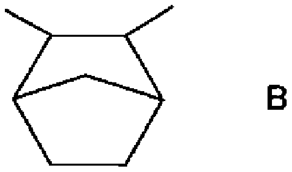
  • the norbornene-based polymer one having at least one repeating unit represented by the following chemical formula 2 (Structural Formula B), that is, an addition (co) polymer is preferable. This is preferable because it is rich in transparency, heat resistance and flexibility.
  • the strong norbornene-based polymer is, for example, a norbornene-based monomer (described later) It is preferably synthesized by using a norbornene monomer represented by the chemical formula 4 or a crosslinkable norbornene monomer.
  • polymer 915 having a relatively high refractive index a monomer having an aromatic ring (aromatic group), a nitrogen atom, a bromine atom or a chlorine atom in the molecular structure is generally used.
  • polymer 915 is synthesized (polymerized).
  • polymer 915 having a relatively low refractive index polymer 915 is synthesized by generally selecting monomers having an alkyl group, a fluorine atom or an ether structure (ether group) in the molecular structure. (Polymerization).
  • the norbornene-based polymer having a relatively high refractive index is preferably a polymer containing a repeating unit of aralkyl norbornene. Strong norbornene-based polymers have a particularly high refractive index.
  • the aralkyl group (arylalkyl group) possessed by the repeating unit of aralkyl norbornene includes, for example, benzyl group, phenyl group, phenylpropyl group, phenylbutyl group, naphthylpropyl group, naphthylpropyl group, fluorine -The ability to mention a ruethyl group, a fluoropropyl group, etc.
  • a benzyl group and a phenylethyl group are particularly preferred.
  • the norbornene-based polymer having a strong repeating unit is preferable because it has an extremely high refractive index!
  • the norbornene-based polymer preferably contains a repeating unit of alkylnorbornene! /. Since a norbornene-based polymer containing an alkylnorbornene repeating unit has high flexibility, high flexibility can be imparted to the optical waveguide 90 by using a strong norbornene-based polymer.
  • Examples of the alkyl group that the alkylnorbornene repeating unit has include a propyl group, a butyl group, a pentyl group, a hexyl group, a heptyl group, an octyl group, a nonyl group, and a decyl group.
  • the group is particularly preferred.
  • These alkyl groups may be linear or branched.
  • the repeating unit of hexylnorbornene By including the repeating unit of hexylnorbornene, it is possible to prevent the refractive index of the entire norbornene-based polymer from being lowered and to maintain high flexibility.
  • the powerful norbornene-based polymer has a wavelength region as described above (especially around 850 nm). This is preferable because of its excellent transmittance for light in the wavelength region.
  • norbornene-based polymers include hexyl norbornene homopolymer, fueno-noleno norebonenen homopolymer, benzenonono levonolene homopolymer, hexyl norbornene and Copolymers with pheyl-ruethyl norbornene, copolymers of hexyl norbornene and benzyl norbornene, and the like, are not limited thereto.
  • the core layer forming material 900 of this embodiment includes, as the additive 920, a monomer, a promoter (first substance), and a catalyst precursor (second substance).
  • the monomer reacts with an actinic radiation, which will be described later, to react in the active radiation irradiated region to form a reactant. And a compound that can cause a difference in refractive index.
  • a polymer (polymer) formed by polymerizing monomers in a polymer (matrix) 915, a cross-linked structure that cross-links the polymers 915, and a polymer 915 branched structures branched from polymer 915 (branched polymer or side chain (pendant group)) can be mentioned.
  • the polymer 915 having a relatively low refractive index and a high refractive index with respect to the polymer 915 are obtained.
  • a polymer having a relatively high refractive index and a monomer having a low refractive index with respect to this polymer 915, in the case where a lower refractive index in the irradiated region is desired. are used in combination.
  • Such a monomer is not particularly limited as long as it is a compound having a polymerizable site, and examples thereof include norbornene monomers, acrylic acid (methacrylic acid) monomers, epoxy monomers, and styrene monomers. 1 or 2 of these A combination of more than one species can be used.
  • a norbornene-based monomer as the monomer.
  • the core layer 93 optical waveguide 90
  • the core layer 93 optical waveguide 90
  • the norbornene-based monomer is a generic term for monomers containing at least one norbornene skeleton represented by the following chemical formula 3 (structural formula A), for example, a compound represented by the following chemical formula 4 (structural formula C) Is mentioned.
  • a represents a single bond or a double bond! ⁇ To each independently represent a hydrogen atom, a substituted or unsubstituted hydrocarbon group, or a functional substituent, and m represents an integer of 0 to 5. However, when a is a double bond, either one of R 1 and R 2 or one of R 3 and R 4 does not exist. ]
  • Examples of the unsubstituted hydrocarbon group include, for example, a linear or branched alkyl group having 1 to 10 carbon atoms (C to C), and a linear or branched carbon number. 2 to 10 (C to C).
  • R 1 and R 2 , R 3 and R 4 are each an alkylidur group having 1 to 10 carbon atoms (C to C). There may be.
  • alkyl group examples include methyl group, ethyl group, propyl group, isopropyl group, butyl group, isobutyl group, sec butyl group, tert butyl group, pentyl group, neopentyl group, hexyl group, heptyl group. Forces including, but not limited to, octyl, nor and decyl groups.
  • alkenyl group examples include, but are not limited to, a vinyl group, an aryl group, a butyr group, and a cyclohexenyl group.
  • alkyl group examples include, but are not limited to, an ether group, a 1-propyl group, a 2-propyl group, a 1-buturyl group, and a 2-butynyl group.
  • cycloalkyl group include force S including, but not limited to, a cyclopentyl group, a cyclohexyl group, and a cyclooctyl group.
  • aryl groups include, but are not limited to, phenyl groups, naphthyl groups, and anthracenyl groups.
  • aralkyl group examples include, but are not limited to, a benzyl group and a phenethyl group.
  • alkylidenyl group examples include, but are not limited to, a methylidenyl group and an ethylidenyl group.
  • Examples of the substituted hydrocarbon group include those in which part or all of the hydrogen atoms of the hydrocarbon group are substituted with halogen atoms, that is, halohyd rocarbyl, nonrorono And a halogenated hydrocarbon group such as a force perhalocarbyl group which is a perhalohydrocarbyl group.
  • the halogen atom substituted for the hydrogen atom is preferably at least one selected from a chlorine atom, fluorine and bromine, more preferably a fluorine atom.
  • perhalogenated hydrocarbon groups include, for example, perfluorophenol group, perfluoromethyl group (trifluoromethyl group).
  • halogenated alkyl group those having 11 to 20 carbon atoms can be suitably used in addition to those having 1 to 10 carbon atoms.
  • a halogenoalkyl group is partially or completely halogenated, linear or branched, and is represented by the general formula: C X ′ ′
  • Z 2Z + 1 groups can be selected.
  • the substituted hydrocarbon group includes a linear or branched alkyl group or haloalkyl group having 1 to 5 carbon atoms (C to C), an aryl group, and a cyclo group.
  • Examples thereof include a cycloalkyl group, an aryl group, an aralkyl group (araalkyl group) and the like which are further substituted with an alkyl group.
  • Examples of the functional substituent include one (CH) one CH (CF) -O-Si (Me), one (
  • n represents an integer of 0 to 10
  • R 5 each independently represents a hydrogen atom, a linear or branched carbon number of 1 to 20 (C
  • Alkyl group linear or branched carbon number 2-10 (C
  • the hydrocarbon group represented by R 5 represents the same hydrocarbon group as represented by I ⁇ to R 4 . As indicated by I ⁇ to R 4 , the hydrocarbon group represented by R 5 may be halogenated or perhalogenated.
  • R 5 is a halogenated or perhalogenated alkyl having 1 to 20 carbon atoms (C 1 to C 6).
  • R 5 is represented by the general formula: CX ′ ′. Where z and X, are
  • X ′ ′ is a halogen atom (for example, a fluorine atom, a chlorine atom or a fluorine atom).
  • the perhalogenated alkyl group is a group in which all X ', in the above general formula is a halogen atom. Specific examples thereof include a trifluoromethyl group, Forces including, but not limited to, trichloromethyl groups, CF, and CF.
  • perhalogenated aryl group examples include, but are not limited to, a pentachlorophenol group and a pentafluorophenyl group.
  • R 6 for example, C (CH 3), 1 Si (CH 2), 1 CH (R 7 ) — O—CH 2 CH
  • R 7 is a hydrogen atom, or a linear or branched carbon number of 1 to 5 (C to C).
  • 1 5 represents an alkyl group.
  • alkyl group examples include a methyl group, an ethyl group, a propyl group, an i-propyl group, a butyl group, an i-butyl group, a t-butyl group, a pentyl group, a t-pentyl group, and a neopentyl group.
  • an ester bond is formed between the single bond extending from the ring structure and the acid substituent.
  • R 6 include, for example, 1-methyl-1-cyclohexyl group, isobornyl group, 2-methyl-2-isobornyl group, 2-methyl-2-adamantyl group.
  • R 6 examples include a dicyclopropylmethyl group (Dcpm) and a dimethylcyclopropylmethyl group (Dmcp) represented by the following chemical formula 6.
  • crosslinking monomer a crosslinking monomer (crosslinking agent) may be used instead of the above monomer or together with the above monomer.
  • This crosslinkable monomer is a compound capable of causing a crosslinking reaction in the presence of a catalyst precursor described later.
  • the use of the crosslinkable monomer has the following advantages. That is, since the crosslinkable monomer is polymerized more quickly, the time required for the formation (process) of the core layer 93 (optical waveguide 90) can be shortened. Further, since the crosslinkable monomer is difficult to evaporate even when heated, an increase in vapor pressure can be suppressed. Furthermore, since the crosslinkable monomer is excellent in heat resistance, the heat resistance of the core layer 93 can be improved.
  • the crosslinkable norbornene-based monomer is a compound including a norbornene-based moiety (norbornene-based double bond) represented by the above chemical formula 3 (Structural Formula A).
  • Crosslinkable norbornene-based monomers include fused multicyclic ring systems and linked multicyclic ring systems CO compounds.
  • Y represents a methylene (—CH—) group
  • m represents an integer of 0 to 5.
  • norbornadiene is considered to be included in a continuous polycyclic ring system and include a polymerizable norbornene double bond.
  • examples of the linked polycyclic ring system compound include compounds represented by the following chemical formula (9).
  • a independently represents a single bond or a double bond; m independently represents an integer of 0 to 5; and R 9 independently represents a divalent carbonization. It represents a hydrogen group, a divalent ether group or a divalent silyl group. N is 0 or 1.
  • the divalent substituent means a group having two bonds that can be bonded to the norbornene structure at the end.
  • divalent hydrocarbon group examples include an alkylene group represented by the general formula: — (CH 2) — d 2d (d is preferably an integer of 1 to 10 )) And divalent aromatic groups (aryl groups).
  • divalent alkylene group a linear or branched carbon number of 1 to 10 (C
  • alkylene groups are preferred, for example, methylene, ethylene, propylene, butylene, pentylene, hexylene, heptylene, octylene, nonylene, decylene. Is mentioned.
  • the branched alkylene group is one in which a hydrogen atom in the main chain is substituted with a linear or branched alkyl group.
  • the divalent aromatic group is preferably a divalent phenyl group or a divalent naphthyl group.
  • R 10 - is a group represented by - O-R 10.
  • each R 10 independently represents the same as R 9 .
  • the compound represented by this chemical formula 11 is dimethylbis [bicyclo [2.2.1] hept-2-ene-5-methoxy] silane, and in its name, dimethylbis (norbornenemethoxy) silane. (Abbreviated as rsixj).
  • SiX dimethylbis (norbornene methoxy) silane
  • SiX has a sufficiently low refractive index for norbornene-based polymers containing repeating units of alkylnorbornene and repeating units of Z or aralkylnorbornene.
  • the clad portion 95 can be formed by reliably lowering the refractive index of the irradiation region irradiated with actinic radiation described later. Further, the difference in refractive index between the core portion 94 and the clad portion 95 can be increased, and the characteristics (optical transmission performance) of the core layer 93 (optical waveguide 90) can be improved.
  • the catalyst precursor (second substance) is a substance capable of initiating the above-described monomer reaction (polymerization reaction, cross-linking reaction, etc.), and is a cocatalyst activated by irradiation with actinic radiation described later ( The substance whose activation temperature changes due to the action of the first substance).
  • the catalyst precursor (procatalyst)
  • V or any compound may be used as long as the activation temperature changes (increases or decreases) with irradiation of actinic radiation.
  • the temperature of the actinic acid decreases with irradiation of actinic radiation.
  • the core layer 93 optical waveguide 90
  • the core layer 93 optical waveguide 90
  • a catalyst precursor one containing (mainly) at least one of the compounds represented by the following formulas (la) and (lb) is preferably used.
  • R represents a hydrogen atom (or one of its isotopes) or a moiety containing a hydrocarbon group
  • Q represents a carboxylate
  • LB represents a Lewis base
  • WCA represents a weakly coordinated anion
  • a represents an integer of 1 to 3
  • b represents an integer of 0 to 2
  • p and r represent numbers that balance the charge of the palladium cation and the weakly coordinated ion.
  • Typical catalyst precursors according to formula la include Pd (OAc) (P (i-Pr)), Pd (OAc) (
  • Cp represents a cyclopentyl group
  • Cy represents a cyclohexyl group
  • the catalyst precursor represented by the formula lb a compound in which p and r are also selected as an integer force of 1 and 2, respectively, is preferable.
  • Typical catalyst precursors according to such a formula lb include Pd (OAc) (P (Cy)).
  • Cy represents a cyclohexyl group
  • Ac represents a acetyl group
  • These catalyst precursors can efficiently react with a monomer (in the case of a norbornene-based monomer, an efficient polymerization reaction, a crosslinking reaction, etc. by an addition polymerization reaction).
  • the activity temperature is lower by about 10 to 80 ° C. (preferably about 10 to 50 ° C.) than the original activity temperature.
  • the activity temperature is lower by about 10 to 80 ° C. (preferably about 10 to 50 ° C.) than the original activity temperature.
  • Pd (OAc) (P (i-Pr)) and Pd (OAc) (P (Cy)) are powerful catalyst precursors.
  • Pd (OAc) P (i-Pr)
  • Pd545" Pd (OAc) (P (Cy)
  • the cocatalyst (first substance) can be activated by irradiation with actinic radiation to change the activation temperature of the catalyst precursor (procatalyst) (the temperature causing the monomer to react). It is a substance.
  • V or any compound can be used as long as it is a compound that changes its activity (reaction or decomposition) upon irradiation with actinic radiation. Force that can be decomposed by irradiation with actinic radiation of a specific wavelength to generate cations such as protons and other cations, and weakly coordinated ions (WC A) that can be substituted for the leaving groups of the catalyst precursor.
  • the compound containing (mainly) the compound (photoinitiator) is preferably used.
  • Examples of weakly coordinated ions include tetrakis (pentafluorophenyl) borate ion.
  • FABA- hexafluoroantimonate ion
  • SBF- hexafluoroantimonate ion
  • Examples of the cocatalyst include tetrakis (pentafluorophenol) borate and hexafluoroantimonic acid represented by the following chemical formula 18.
  • RHODORSIL registered trademark, the same shall apply hereinafter
  • PHO TOINITIATOR 2074 available from Rhodia USA, Cranberry, NJ No.
  • TAG— 372R ((Dimethyl (2- (2 naphthyl) -2—oxoethyl) sulfo-tetrakis (pentafluorophenol) borate: available from Toyo Ink Manufacturing Co., Ltd., Tokyo, Japan: CAS No. 193957—54—No. 9)
  • MPI-103 CAS No. 87709—41—No. 9” available from Midori Chemical Co., Tokyo, Japan.
  • TAG—371 (CAS number 193957—53—8)” available from the company
  • TBPS—TPFPB (4 tert butylphenol) sulfone available from Toyo Gosei Co., Ltd., Tokyo, Japan -Umtetrakis (pentapentafluo Hue - Le) volley And “NAI-105 (CAS No. 85342-62-7)” available from Midori Chemical Co., Ltd., Tokyo, Japan.
  • UV light ultraviolet light
  • actinic radiation actinic radiation
  • a mercury lamp high pressure mercury lamp
  • ultraviolet rays (active radiation) having sufficient energy of less than 300 nm can be supplied to the layer 910, and RHODORSIL PHOTOINITIATOR 2074 can be efficiently decomposed to generate the above-mentioned cations and WCA. it can.
  • a sensitizer may be added to the core layer forming material (varnish) 900 as necessary.
  • the sensitizer increases the sensitivity of the promoter to actinic radiation, reduces the time and energy required for activation (reaction or decomposition) of the promoter, and a wavelength suitable for activation of the promoter. It has a function of changing the wavelength of actinic radiation.
  • Such a sensitizer is appropriately selected according to the sensitivity of the promoter and the peak wavelength of absorption of the sensitizer, and is not particularly limited.
  • 9, 10 dibutoxyanthracene (CAS No. Anthracene, xanthones, anthraquinones, phenanthrenes, thalicenes, benzpyrenes, fluoranthenes, rubrenes, pyrenes, indanthrenes, thixanthene, etc.
  • Examples thereof include thioxanthe n-9-ones, and these can be used alone or as a mixture.
  • sensitizer examples include 2-isopropyl-9H thixanthene-9-one, 4-isopropinole-9H-thixanthene 9one, 1 chloro-4 propoxythioxanthone, phenothiazine, or a mixture thereof. Is mentioned.
  • DBA Dibutoxyanthracene
  • the content of the sensitizer in the core layer forming material 900 is not particularly limited, but is preferably 0.01% by weight or more, more preferably 0.5% by weight or more. More preferably, it is 1% by weight or more. The upper limit is preferably 5% by weight or less.
  • an antioxidant may be added to the core layer forming material 900. to this Thus, generation of undesirable free radicals and natural acid generation of polymer 915 can be prevented. As a result, it is possible to improve the characteristics of the obtained core layer 93 (optical waveguide 90).
  • antioxidants include Ciba (registered trademark, the same applies hereinafter) IRGANOX (registered trademark, the same applies hereinafter) 1076 and Ciba IRGAFOS available from Ciba Specialty Chemicals, Tarrytown, NY (Registered trademark, the same shall apply hereinafter) 168 is preferably used.
  • anti-oxidation agents include, for example, Ciba Irganox (registered trademark, the same shall apply hereinafter) 129, Ciba Irganox 1330, Ciba Irganox 1010, Ciba Cyanox (registered trademark, applicable hereinafter) 1790, Ciba Irganox (registered trademark) 3114, Ciba Irganox 3125, etc. can also be used.
  • Such an antioxidant can be omitted, for example, when the layer 910 is not exposed to oxidation conditions or when the exposure period is extremely short.
  • Core layer forming material (varnish)
  • the solvent used for the preparation of 900 is, for example, jetyl ether, diisopropyl ether, 1,2-dimethoxyethane (DME), 1,4-dioxane, tetrahydrofuran (THF ), Tetrahydropyran (THP), vinyl, diethylene glycol dimethyl ether (diglyme), ether solvents such as diethylene glycol ether ether (carbitol), methyl caffeine solvate, cetyl caffeosolve, ferrous caffeine solvate, etc.
  • Cellosolve solvents aliphatic hydrocarbon solvents such as hexane, pentane, heptane, cyclohexane, aromatic hydrocarbon solvents such as toluene, xylene, benzene, mesitylene, pyridine, pyrazine, furan, pyrrole, thiophene, Aromatic heterocyclic compounds such as methylpyrrolidone, N, N-dimethylform Amide solvents such as amide (DMF), N, N-dimethylacetamide (DMA), halogen compound solvents such as dichloromethane, chloroform, 1,2-dichloroethane, ester systems such as ethyl acetate, methyl acetate, ethyl formate Examples thereof include various organic solvents such as solvents, sulfur compound solvents such as dimethyl sulfoxide (DMSO) and sulfolane, and mixed solvents containing these.
  • DMF amide
  • DMA
  • methods for removing (desolving) the solvent from the liquid film formed on the support substrate 951 include, for example, natural drying, heating, leaving under reduced pressure, and blowing an inert gas (blowing). ) The method of forced drying by etc. is mentioned.
  • the layer 910 that is a film-like solidified product (or cured product) of the core layer forming material 900 is formed on the support substrate 951.
  • the layer (dry film of PITDM) 910 has a first refractive index (RI). This first refractive index is due to the action of polymer 915 and monomers that are uniformly dispersed (distributed) in layer 910.
  • a mask (masking) 935 in which an opening (window) 9351 is formed is prepared, and the layer 910 is irradiated with active radiation (active energy beam) 930 through the mask 935. (See Figure 3).
  • the irradiation region 925 of the active radiation 930 becomes the clad portion 95.
  • an opening (window) 9351 equivalent to the pattern of the clad portion 95 to be formed is formed in the mask 935.
  • the opening 9351 forms a transmission part through which the active radiation 930 to be irradiated passes.
  • the mask 935 may be formed in advance (separately formed) (for example, plate-shaped) or formed on the layer 910 by, for example, a vapor deposition method or a coating method.
  • Preferred examples of the mask 935 include a photomask made of quartz glass or a PET base material, a stencil mask, a metal thin film formed by a vapor deposition method (evaporation, sputtering, etc.), and the like. Among these, it is particularly preferable to use a photomask or stencil mask. This is because a fine pattern can be formed with high accuracy and is easy to handle, which is advantageous in improving productivity.
  • an opening (window) 9351 equivalent to the pattern of the clad portion 95 to be formed is obtained by partially removing the mask along the pattern of the non-irradiated region 940 of the active radiation 930.
  • active radiation composed of a shielding material made of a metal such as chromium on the photomask.
  • a wire 930 provided with a shielding portion can also be used.
  • the part other than the shielding part is the window (transmission part).
  • the actinic radiation 930 to be used is not limited as long as it can cause a photochemical reaction (change) to the cocatalyst.
  • a photochemical reaction change
  • visible light, ultraviolet light, infrared light, laser light, Electron beams and X-rays can also be used.
  • the actinic radiation 930 is appropriately selected depending on the type of cocatalyst and the type of sensitizer when it contains a sensitizer, and is not particularly limited, but in the wavelength range of 200 to 450 nm. It is preferable to have a peak wavelength. Thereby, the cocatalyst can be activated relatively easily.
  • the irradiation dose of the actinic radiation 930 is preferably in the range of about 0. l ⁇ 9jZcm 2 instrument 0.2
  • ⁇ 6JZcm 2 about a and even and even have further preferred more preferred instrument 0. 2 ⁇ 3jZcm 2 about. Thereby, a promoter can be activated reliably.
  • the co-catalyst first substance: cocatalyst
  • the co-catalyst first substance: cocatalyst
  • the co-catalyst reacts (bonds) or decomposes by the action of 930 to release (generate) cations (protons or other cations) and weakly coordinated ions (WCA).
  • the catalyst precursor in the active latent state is a force in which the active temperature is lower than the original activation temperature, that is, at about room temperature.
  • the catalyst precursor is in a state in which the monomer reaction cannot be caused in the irradiation region 925.
  • the layer 910 is subjected to heat treatment (first heat treatment).
  • the catalyst precursor in the active latent state is activated (becomes active), and monomer reaction (polymerization reaction or cross-linking reaction) occurs.
  • the amount of monomer decreases as the monomer diffuses into the region force irradiated region 925, so that the influence of the polymer 915 appears greatly on the refractive index of the region.
  • the third refractive index is higher than the first refractive index.
  • the heating temperature in this heat treatment is not particularly limited, but is preferably about 30 to 80 ° C, more preferably about 40 to 60 ° C.
  • the heating time is preferably set so that the reaction of the monomer in the irradiation region 925 is almost completed. Specifically, it is preferably about 0.1 to 2 hours. More preferably, it is about 1 to 1 hour.
  • the layer 910 is subjected to a second heat treatment.
  • the catalyst precursor remaining in the unirradiated region 940 and Z or irradiated region 925 is activated (activated) directly or with the activity of the promoter.
  • the heating temperature in the second heat treatment is not particularly limited as long as it can activate the catalyst precursor or the cocatalyst, but is preferably about 70 to 100 ° C.
  • the heating time is preferably about 0.5 to 2 hours, and more preferably about 0.5 to 1 hour.
  • the layer 910 is subjected to a third heat treatment.
  • the internal stress generated in the obtained core layer 93 can be reduced, and the core portion 94 and the clad portion 95 can be further stabilized.
  • the heating temperature in this third heat treatment is 2 than the heating temperature in the second heat treatment.
  • the temperature is preferably about 90 to 180 ° C., more preferably about 120 to 160 ° C.
  • the heating time is preferably about 0.5 to 2 hours, more preferably about 0.5 to 1 hour.
  • the core layer 93 is obtained through the above steps.
  • the cladding layer 91 (92) is formed on the support substrate 952 (see FIG. 5).
  • the clad layer 91 (92) can be formed by applying a varnish containing a clad material (clad layer forming material) and curing (solidifying), or applying a curable monomer composition and curing (solidifying). B) It is possible to use any method that is appropriate for V.
  • the clad layer 91 (92) is formed by a coating method
  • examples thereof include a spin coating method, a dating method, a table coating method, a spray method, an applicator method, a curtain coating method, and a die coating method.
  • the support substrate 952 a substrate similar to the support substrate 951 can be used.
  • the clad layer 91 (92) As a constituent material of the clad layer 91 (92), a material mainly composed of a norbornene-based polymer is used. Since norbornene-based polymers have excellent heat resistance, this is applied to the cladding layer 91 (92) In the optical waveguide 90 used as a constituent material, the conductor layers 901 and 902 are formed on the optical waveguide 90, the conductor layers 901 and 902 are processed to form the wiring, the optical elements are mounted, etc. Even so, it is possible to prevent the cladding layer 91 (92) from softening and deforming.
  • Norbornene-based polymers or norbornene-based monomers that are raw materials thereof are also preferable because they are relatively inexpensive and easily available.
  • the material of the clad layer 91 (92) becomes the same kind as the material suitably used as the constituent material of the core layer 93.
  • the adhesion between the clad layer 91 (92) and the core layer 93 can be prevented from being separated. For this reason, the optical waveguide 90 having excellent durability can be obtained.
  • Examples of such norbornene-based polymers include (1) a norbornene-type monomer-attached (co) polymer obtained by subjecting a norbornene-type monomer to an appendage (co) polymerization, and (2) norbornene. Attached copolymer such as a copolymer with an ethylene monomer and ⁇ -olefins, (3) a copolymer with a norbornene monomer and a non-conjugated gen, and optionally with other monomers.
  • ring-opening (co) polymer of norbornene-type monomer and, if necessary, hydrogenated hydrogenated (co) polymer, (5) norbornene-type monomer and ethylene or a one-year-old refins
  • a ring-opening copolymer with, and optionally a hydrogenated hydrogenated (co) polymer (6) a ring-opening copolymer of a norbornene-type monomer with a non-conjugated gen, or another monomer, and If necessary, the (co) polymer is watered.
  • Ring-opening polymer and the like such as the addition polymer. Examples of these polymers include random copolymers, block copolymers, and alternating copolymers.
  • norbornene polymers include, for example, ring-opening metathesis polymerization (ROMP), combination of ROM P and hydrogenation reaction, polymerization by radical or cation, polymerization using cationic palladium polymerization initiator, and others.
  • ROMP ring-opening metathesis polymerization
  • combination of ROM P and hydrogenation reaction polymerization by radical or cation
  • polymerization using cationic palladium polymerization initiator and others.
  • Can be obtained by all known polymerization methods such as polymerization using a polymerization initiator (eg, polymerization initiator of nickel or other transition metal). wear.
  • an addition (co) polymer is preferable. This is preferable because it is rich in transparency, heat resistance and flexibility.
  • the norbornene-based polymer preferably includes a norbornene repeating unit having a substituent containing a polymerizable group.
  • the polymerizable groups of at least a part of the norbornene-based polymer can be crosslinked directly or via a crosslinking agent.
  • the kind of the crosslinking agent, the kind of the polymer used for the core layer 93, the norbornene-based polymer and the polymer used for the core layer 93 can be crosslinked. In other words, it is preferable that at least a part of the strong norbornene-based polymer is cross-linked with the polymerizable group.
  • the strength of the clad layer 91 (92) itself can be improved, and the adhesion between the clad layer 91 (92) and the core layer 93 can be improved.
  • an epoxy group is preferable because it includes one or a combination of two or more of an epoxy group, a (meth) acrylic group, an alkoxysilyl group, and the like. Epoxy groups are preferred because of their high reactivity among various polymerizable groups.
  • the norbornene-based polymer preferably includes an alkylnorbornene repeating unit.
  • the alkyl group may be linear or branched. Since the norbornene-based polymer containing a repeating unit of alkyl norbornene has high flexibility, high flexibility (flexibility) can be imparted to the optical waveguide 90 by using a strong norbornene-based polymer.
  • a norbornene-based polymer containing an alkylnorbornene repeating unit is also preferable because of its excellent transmittance with respect to light in the wavelength region as described above (particularly in the wavelength region near 850 nm).
  • the norbornene-based polymer used for the clad layer 91 (92) is preferably represented by the following chemical formula 19.
  • R represents an alkyl group having 1 to 10 carbon atoms
  • a represents an integer of 0 to 3
  • b represents an integer of 1 to 3
  • pZq is 20 or less.
  • the powerful norbornene-based polymer has a relatively low! And refractive index.
  • the clad layer 91 (92) using the strong norbornene-based polymer as a main material, The optical transmission performance of the optical waveguide 90 can be further improved.
  • R is an alkyl group having 4 to 10 carbon atoms
  • a and b are each 1, for example, butylbornene and methyl
  • a copolymer of daricidyl ether norbornene, a copolymer of hexyl norbornene and methyl daricidyl ether norbornene, a copolymer of decyl norbornene and methyl darcydyl ether norbornene, and the like are preferable.
  • pZq may be 20 or less, but is preferably 15 or less, more preferably about 0.1 to 10. As a result, the effect of including two kinds of norbornene repeating units is exhibited.
  • the same kind of the above-mentioned promoter is used in the cladding layer forming material.
  • This substance photoacid generator or photobase generator
  • the epoxy group may be cleaved and crosslinked by the action of this substance.
  • a clad layer type is further used.
  • a compound having at least one epoxy group may be mixed as a crosslinking agent in the composition material.
  • cross-linking agents examples include 3-glycidoxypropyltrimethoxysilane ( ⁇ -
  • GPS silicone epoxy resin and the like are preferably used.
  • the crosslinking reaction between the epoxy groups may be performed in the final stage of this step [6 [].
  • additives may be added (mixed) to the cladding layer forming material.
  • the monomer, catalyst precursor, and co-catalyst mentioned in the core layer forming material may be mixed as an additive.
  • the monomer in the clad layer 91 (92), the monomer can be reacted in the same manner as described above to change the refractive index of the clad layer 91 (92).
  • Examples of the other additives include the above-described anti-oxidation agent.
  • an antioxidant By mixing an antioxidant, it is possible to prevent deterioration of the clad material (norbornene polymer) due to oxidation.
  • the clad layer 91 (92) is formed on the support substrate 952.
  • the core layer 93 is peeled from the support substrate 951, and the core layer 93 is divided into a support substrate 952 on which the cladding layer 91 is formed and a support substrate 952 on which the cladding layer 92 is formed. Hold it (see Fig. 6).
  • the upper surface of the support substrate 952 on which the cladding layer 92 is formed is formed. Pressure is applied from the surface side, and the clad layers 91 and 92 and the core layer 93 are pressure bonded.
  • the clad layers 91 and 92 and the core layer 93 are joined and integrated.
  • the crimping operation is preferably performed under heating.
  • the heating temperature is the cladding layer 9
  • the support substrate 952 is peeled off and removed from the clad layers 91 and 92, respectively. Thereby, the optical waveguide 90 of the present invention is obtained.
  • conductor layers 901 and 902 are formed on the upper and lower surfaces of the optical waveguide 90, respectively (see FIG. 7).
  • Each of the conductor layers 901 and 902 can be formed by, for example, a chemical vapor deposition method (CVD method) such as a plasma CVD method, a thermal CVD method, or a laser CVD method, a vacuum evaporation method, a spade method, etc.
  • CVD method chemical vapor deposition method
  • Electrical methods such as dry plating methods such as physical vapor deposition methods (PVD methods) such as attering methods and ion plating methods, wet plating methods such as electrolytic plating, immersion plating and electroless plating, and laminating methods.
  • PVD methods physical vapor deposition methods
  • wet plating methods such as electrolytic plating, immersion plating and electroless plating, and laminating methods.
  • At least one of the sheet material joints can be used. As a result, high adhesion between the conductor layers 901 and 902 and the optical waveguide 90 can be obtained.
  • the optical waveguide structure 9 of the present invention is completed.
  • the core portion 94 is composed of the first norbornene-based material as the main material, and the cladding portion 95 is lower than the first norbornene-based material.
  • a second norbornene-based material having a refractive index is used as a main material, and a norbornene-based polymer having a refractive index lower than that of the first norbornene-based material (the core portion 94 of the core layer 93) is used for each of the cladding layers 91 and 92. Constructed as the main material.
  • the first norbornene-based material and the second norbornene-based material both have a force containing the same norbornene-based polymer.
  • the reaction product of the norbornene-based monomer having a refractive index different from that of the norbornene-based polymer.
  • the refractive indexes differ from each other due to the difference in the content of.
  • the optical waveguide structure 9 having a strong structure can provide high optical transmission performance of the optical waveguide 90.
  • the optical waveguide 90 (optical waveguide structure 9) having such a configuration has excellent durability.
  • the conductor layer 901 can be applied by employing various methods as described above while preventing deterioration (deterioration) of the characteristics. 902 can be reliably formed. In particular, even when the conductor layers 901 and 902 are formed so as to overlap with the core portion 94 important for light transmission, the core portion 94 can be prevented from being deteriorated and deteriorated.
  • the optical waveguide structure 9 having the core part 94 having a desired shape and high dimensional accuracy can be obtained by a simple process and in a short time. Obtainable.
  • the second manufacturing method is the same as the first manufacturing method except that the composition of the core layer forming material 900 is different.
  • the core layer forming material 900 used in the second production method includes a release agent (substance) that is activated by irradiation with actinic radiation, and a main chain and a release branched from the main chain and activated. And a polymer 915 having a leaving group (leaving pendant group) capable of leaving at least a part of the molecular structure from the main chain by the action of the agent.
  • the same promoter as that mentioned in the first production method can be used.
  • the polymer 915 used in the second production method is the same as in the first production method. Examples thereof include those obtained by substituting the substituents of the exemplified polymer 915 with a leaving group, and those obtained by introducing a leaving group into the polymer 915 mentioned in the first production method.
  • Powerful polymer 915 has its refractive index changed (increased or lowered) by the elimination (cleavage) of the leaving group.
  • the leaving group is a group that is released by the action of a cation, cation, or free radical, that is, an acid (cation) leaving group, a base (an) leaving group, or a free radical leaving group.
  • the group may be displaced, but is preferably a group (acid group leaving group) that is released by the action of a cation (proton).
  • the acid leaving group includes, in its molecular structure, —O structure, —Si—aryl structure and
  • At least one of a 1 Si diphenyl structure and an O Si diphenyl structure is preferred.
  • examples of the free radical-leaving group capable of leaving by the action of free radicals include a substituent having a acetophenone structure at the terminal.
  • the polymer 915 includes a repeating unit of alkyl (particularly hexyl) norbornene for which it is preferable to use a norbornene-based polymer for the same reason as described in the first production method. It is more preferable to use a norbornene-based polymer.
  • polymers 915 whose refractive index decreases due to leaving group leaving include homopolymers of diphenylmethylnorbornenemethoxysilane, hexylnorbornene and diphenylmethylnorbornenemethoxysilane. Are preferably used.
  • the polymer 915 will be described in which a polymer whose refractive index decreases due to the removal of a leaving group (particularly an acid leaving group).
  • the irradiation region 925 of the active radiation 930 becomes the clad portion 95.
  • step [1B] A step similar to the step [1A] is performed.
  • the layer (dry film of PITDM) 910 has a first refractive index (RI). This first refractive index is due to the action of polymer 915 that is uniformly dispersed (distributed) in layer 910.
  • the release agent present in the irradiation region 925 irradiated with the actinic radiation 930 reacts (bonds) or decomposes by the action of the actinic radiation 930, and Cations (protons or other cations) and weakly coordinated ions (
  • the cation cleaves the leaving group itself from the force to release the main chain force or from the middle of the molecular structure of the leaving group (photo bleach).
  • the irradiated region 925 the number of leaving groups in a complete state is reduced compared to the unirradiated region 940, and the second refractive index is lower than the first refractive index. At this time, the refractive index of the unirradiated region 940 is maintained at the first refractive index.
  • a release agent can be activated reliably.
  • the releasable basic force released (cut) from the polymer 915 is removed from, for example, the irradiated region 925, or rearranged or cross-linked in the polymer 915.
  • the refractive index difference between the core portion 94 and the cladding portion 95 can be further increased.
  • the heating temperature in this heat treatment is not particularly limited, but is preferably about 70 to 195 ° C, more preferably about 85 to 150 ° C.
  • the heating time is sufficient to remove the leaving group that has been detached (cleaved) from the irradiation region 925.
  • it is preferably about 0.5 to 3 hours, and more preferably about 0.5 to 2 hours.
  • this step [3B] is omitted when, for example, a sufficient refractive index difference is obtained between the core portion 94 and the cladding portion 95 in the state before the heat treatment. You can do it.
  • a step of one or more heat treatments (for example, about 150 to 200 ° C x about 1 to 8 hours) can be added.
  • the core layer 93 is obtained through the above steps.
  • step [4B] The same step as in step [6A] is performed.
  • the optical waveguide structure 9 of the present invention is completed.
  • the core layer 93 is composed of a norbornene-based material as a main material, and the cladding layers 91 and 92 are each more bent than the core portion 94 of the core layer 93.
  • the main material is a norbornene-based polymer having a low A.
  • the core portion 94 and the clad portion 95 are mainly norbornene-based polymers having a main chain and a leaving group branched from the main chain and having at least a part of the molecular structure capable of leaving the main chain.
  • the core part 94 and the clad part 95 which are configured as materials, have different refractive indexes due to different numbers of leaving groups bonded to the main chain.
  • the optical waveguide structure 9 having a strong structure can provide high optical transmission performance of the optical waveguide 90.
  • the optical waveguide 90 (optical waveguide structure 9) having such a configuration has excellent durability.
  • the conductor layer 901 can be applied by adopting various methods as described above while preventing deterioration (deterioration) of its characteristics. 902 can be reliably formed. In particular, even when the conductor layers 901 and 902 are formed so as to overlap with the core portion 94 important for light transmission, the core portion 94 can be prevented from being deteriorated and deteriorated.
  • the optical waveguide structure 9 having the core part 94 having a desired shape and high dimensional accuracy can be obtained by a simple process and in a short time. Obtainable.
  • the core layer 93 can be formed by an extremely simple process that requires at least active radiation.
  • the core layer forming material 900 As the core layer forming material 900, a combination of the core layer forming materials used in the first and second manufacturing methods is used. This is the same as the manufacturing method 2.
  • the core layer forming material 900 used in the third production method includes the polymer 915 having a leaving group as described above, a monomer, a promoter (first substance), and a catalyst precursor. (Second substance).
  • the cocatalyst is the same as the release agent in the second production method, and also has a function of releasing the release agent.
  • the refractive index between the core portion 94 and the cladding portion 95 in the resulting core layer 93 is determined by the combination of the selected leaving group and the selected monomer. The difference can be adjusted in more stages.
  • a monomer having a refractive index lower than that of polymer 915 is used, and a catalyst precursor having an activation temperature that decreases with irradiation of actinic radiation 930 is used. If polymer 915 whose refractive index decreases due to the removal of the leaving group is used, the irradiated region 925 is the cladding portion 95 and the refractive index difference from the core portion 94 is extremely large. The core layer 93 can be obtained.
  • the irradiation region 925 of the active radiation 930 becomes the clad portion 95.
  • the layer (dry film of PITDM) 910 has a first refractive index (RI). This first refractive index is due to the action of polymer 915 and monomers that are uniformly dispersed (distributed) in layer 910.
  • the cocatalyst (first substance: cocatalyst) existing in the irradiation region 925 irradiated with the actinic radiation 930 is affected by the action of the actinic radiation 930. Reacts or decomposes to release (generate) cations (protons or other cations) and weakly coordinated ions (WCA).
  • the cation is cleaved from the force that causes the leaving group itself to leave the main chain force, or from the middle of the molecular structure of the leaving group.
  • the refractive index of 940 maintains the first refractive index.
  • a promoter can be activated reliably.
  • Step [3A] is performed in a similar manner to step [3A].
  • the catalyst precursor in the active latent state is activated (becomes active), and monomer reaction (polymerization reaction or cross-linking reaction) occurs.
  • monomer reaction polymerization reaction or cross-linking reaction
  • the releasable basic force released (cut) from the polymer 915 for example, removed from the irradiated region 925, or rearranged or cross-linked in the polymer 915.
  • the amount of monomer decreases as the monomer diffuses into the region force irradiated region 925, so that the influence of the polymer 915 appears greatly on the refractive index of the region.
  • the third refractive index is higher than the first refractive index.
  • a refractive index difference (second refractive index ⁇ third refractive index) occurs between the irradiated region 925 and the unirradiated region 940, and the core portion 94 (unirradiated region 940) and A clad portion 95 (irradiation region 925) is formed.
  • the optical waveguide structure 9 of the present invention is completed.
  • the core layer 93 has a main chain and a leaving group that is branched from the main chain, and at least a part of the molecular structure can be detached from the main chain.
  • a norbornene-based polymer that contains a norbornene-based polymer, the core portion 94 and the cladding portion 95 are different in the number of leaving groups bonded to the main chain, and have a different refractive index than the norbornene-based polymer.
  • the cladding layers 91 and 92 are each composed mainly of a norbornene-based polymer having a refractive index lower than that of the core portion 94 of the core layer 93.
  • the optical waveguide structure 9 having a strong structure can provide high optical transmission performance of the optical waveguide 90.
  • the optical waveguide 90 (optical waveguide structure 9) having such a configuration has excellent durability.
  • the conductor layer 901 can be applied by adopting various methods as described above while preventing deterioration (deterioration) of its characteristics. 902 can be reliably formed. In particular, even when the conductor layers 901 and 902 are formed so as to overlap with the core portion 94 important for light transmission, the core portion 94 can be prevented from being deteriorated and deteriorated.
  • the optical waveguide structure 9 having the core part 94 having a desired shape and high dimensional accuracy can be obtained by simple processing and in a short time. Obtainable.
  • the refractive index difference between the core portion 94 and the cladding portion 95 can be set in multiple stages.
  • FIGS. 8 to 13 are cross-sectional views schematically showing process examples of the fourth manufacturing method of the optical waveguide structure of the present invention.
  • the fourth manufacturing method will be described, but the description will focus on the differences from the first to third manufacturing methods, and the description of the same matters will be omitted.
  • the process of forming the optical waveguide 90 is different, and the other processes are the same as those in the first to third manufacturing methods.
  • the same material as described in the first to third manufacturing methods can be used as the cladding layer forming material.
  • the first layer 1110 is formed on the support substrate 1000 by applying the clad layer forming material (first varnish) using the same method as described above. (See Figure 8).
  • the support substrate 1000 a substrate similar to the support substrate 951 can be used.
  • the average thickness of the first layer 1110 is not particularly limited, but is preferably about 5 to 200 m. 10 to: More preferably about LOO m 15 to 65 / ⁇ . More preferably, it is about ⁇ .
  • the core layer forming material (second varnish) is applied using the same method as described above to form the second layer 1120. (See Figure 9).
  • the material for forming the core layer may be applied after the first layer 1110 is almost completely dried, or may be applied before the first layer 1110 is dried. Oh ,.
  • the first layer 1110 and the second layer 1120 are mixed with each other at the interface between them.
  • the adhesion between the clad layer 91 and the core layer 93 can be improved.
  • the first varnish and the second varnish each have a viscosity (normal temperature) of preferably about 100 to 10,000 cP, more preferably about 150 to 5000 cP, and still more preferably about 200 to 3500 cP.
  • a viscosity normal temperature
  • the first layer 1110 and the second layer 1120 can be prevented from being mixed more than necessary at the interface between them, and the thickness of the first layer 1110 and the second layer 1120 can be prevented. Can be prevented from becoming non-uniform.
  • the viscosity of the second varnish is preferably higher than that of the first varnish. Thus, it is possible to reliably prevent the first layer 1110 and the second layer 1120 from being mixed more than necessary at the interface between them.
  • the average thickness of the second layer 1120 is not particularly limited, but is about 5 to 200 m.
  • the preferred range is about 15 to 125 / zm, and the more preferred range is about 25 to 100 / zm.
  • a clad layer forming material (third varnish) is applied onto second layer 1120 using the same method as described above to form third layer 1130. (See Fig. 10).
  • the third layer 1130 can be formed in the same manner as the second layer 1120.
  • the average thickness of the third layer 1130 is not particularly limited, but is preferably about 5 to 200 m. 10 to: More preferably about L00 m 15 to 65 / ⁇ . More preferably, it is about ⁇ .
  • Examples of the solvent removal method include heating, leaving under atmospheric pressure or reduced pressure, and spraying (blowing) an inert gas or the like, and a method using heating is preferred. This makes it possible to remove the solvent relatively easily and in a short time.
  • the heating temperature is preferably about 25 to 60 ° C, more preferably about 30 to 45 ° C.
  • the heating time is preferably about 15 to 60 minutes, more preferably about 15 to 30 minutes.
  • a mask (masking) 935 in which an opening (window) 9351 is formed is prepared, and active radiation (active energy beam) 930 is irradiated to the laminate 2000 through the mask 935. (See Figure 11).
  • the co-catalyst (first substance: cocatalyst) is present in the irradiation region 925 irradiated with the active radiation 930 of the second layer 1120. ) Reacts or decomposes by the action of actinic radiation 930 to release (generate) cations (protons or other cations) and weakly coordinated ions (WCA).
  • the laminated body 2000 is subjected to heat treatment (first heat treatment).
  • first heat treatment first heat treatment
  • the catalyst precursor in the active latent state is activated (becomes active), and monomer reaction (polymerization reaction or cross-linking reaction) occurs.
  • the monomer concentration in the irradiated region 925 gradually decreases. As a result, there is a difference in the monomer concentration between the irradiated region 925 and the unirradiated region 940, and the monomer diffuses from the unirradiated region 940 and should be collected in the irradiated region 925 to eliminate this. .
  • the amount of monomer decreases as the monomer diffuses into the region force irradiated region 925, so that the influence of the polymer 915 greatly appears on the refractive index of the region.
  • the third refractive index is higher than the first refractive index.
  • the laminate 2000 is subjected to a second heat treatment.
  • the catalyst precursor remaining in the unirradiated region 940 and Z or irradiated region 925 is activated (activated) directly or with the activity of the promoter.
  • the stacked body 2000 is subjected to a third heat treatment.
  • the internal stress generated in the obtained core layer 93 can be reduced, and the core portion 94 and the clad portion 95 can be further stabilized.
  • the optical waveguide 90 of the present invention is obtained.
  • conductor layers 901 and 902 are formed on the upper and lower surfaces of the optical waveguide 90, respectively (see FIG. 13).
  • the core portion 94 can be visually confirmed in the laminate 2000 after the first heat treatment.
  • the same yarn formation as that of the second varnish that is, a polymer containing a polymer 915, a monomer, a promoter and a catalyst precursor may be used. Good.
  • the monomer reaction causes the first layer 1110 and the third layer 1130 to cross the interface between the first layer 1110 and the third layer 1130, the second layer 1120, and the Z or forceful interface. It is possible to prevent the clad layers 91 and 92 and the core layer 93 from peeling off more reliably.
  • RI refractive index
  • II Force to use the same monomer as the second layer 1120 as the monomer of the first layer 1110 and the third layer 1130 in the first layer 1110 and the third layer 1130
  • the ratio of the catalyst precursor and the monomer may be adjusted to be lower than that of the second layer 1120.
  • the first varnish and the third varnish include a norbornene-based polymer having a substituent containing an epoxy structure at the terminal and a promoter. .
  • the epoxy structure is cleaved and a reaction (polymerization) of the core layer 93 with the polymer 915 occurs.
  • the adhesion of the cladding layers 91 and 92 to the core layer 93 can be improved.
  • Examples of such norbornene-based polymers include copolymers of hexyl norbornene (HxNB) and norbornene methyldaricidyl ether (AGENB).
  • the co-catalyst when the core layer 93 is formed, it may be selected so as not to activate.
  • a cocatalyst that does not absorb actinic radiation suitable for activating the cocatalyst contained in the second varnish or is activated by the action of heat in place of the actinic radiation should be selected. ⁇ .
  • Examples of such a cocatalyst include a non-absorbing photobase generator (PBG) and a thermal base generator (TBG).
  • PBG photobase generator
  • TBG thermal base generator
  • the optical waveguide structure 9 as described above can pattern the core portion 94 by a simple method of irradiation with actinic radiation, and design the pattern shape of the core portion (optical circuit) 94.
  • the core portion 94 having a high degree of freedom and a high dimensional accuracy can be obtained.
  • the optical waveguide structure 9 can form both the wiring (electrical circuit) and the core part (optical circuit) 94 with a high arrangement density, the optical waveguide structure 9 is efficient in a hybrid optical and electrical circuit. Therefore, it is possible to design a better circuit and to further integrate circuits.
  • Such an optical waveguide structure 9 has a wide range of optical circuit (optical waveguide pattern) and electrical circuit design, good yield, high optical transmission performance, and excellent reliability and durability. Because of its versatility, it can be used for various electronic parts and electronic devices.
  • the supporting substrates 951, 952, and 1000 are removed. However, these are made of a conductive material and can be removed without removing them.
  • the conductor layers 901 and 902 may be used as they are.
  • one or both of the cladding layers 91 and 92 may be omitted as necessary.
  • the method of forming the core layer 93 is not limited to the method described above.
  • the optical waveguide 90 is not limited to the configuration shown in the figure.
  • the optical waveguide 90 may have a configuration in which a plurality of core layers are stacked between two cladding layers. It is possible to have a structure in which a core layer and a core layer are laminated in order. A laminated body in which one core layer is provided between two clad layers is formed by laminating a plurality of layers. Moyo.
  • an inclined surface (reflective surface) inclined by approximately 45 ° with respect to the optical path, that is, the longitudinal direction of the core portion 94 may be formed in the middle of the core portion 94. Thereby, the light (transmission light) propagating through the core portion 94 can be bent by approximately 90 ° on this inclined surface.
  • the optical path of the transmitted light is not only in the core layer 90 (two-dimensional direction) but also in the three-dimensional direction including the thickness direction of the optical waveguide 90. It can be changed.
  • This inclined surface can be formed by, for example, cutting or removing (deleting) the core portion 94.
  • a reflective film such as a multilayer optical thin film or a metal thin film (for example, an aluminum vapor deposition film) or a reflection increasing film may be formed on the inclined surface.
  • optical waveguide and the optical waveguide structure of the present invention have been described based on the illustrated embodiments, the present invention is not limited to these configurations, and the configuration of each part exhibits the same function. It can be replaced with any configuration you get, and any configuration can be added.
  • hexyl norbornene (CAS No. 22094-83-3) is referred to as “HxN BJ and diphenylmethylnorbornene methoxysilane (CAS No. 376634-34-3) as“ diPhNB ”.
  • -Luetylnorbornene (CAS number 29415-09-6) is replaced with PENBJ
  • butylnorbornene (CAS number 22094-81-1) is replaced with BuNB
  • decylnorbornene (CAS number 22094-85- No. 5) “DeNB”
  • benzylnorbornene (CAS No.
  • TMSNB Trimethoxy Cirino Lubornene
  • SiX 1, 1, 3, 3— Tetramethyl-1,3-bis [2- (5-norbornene-2-yl) ethyl] disiloxane (CAS No. 198570-39-7) may be abbreviated as “Si X”.
  • BuNB (10.52g, 0.07mol), AGENB (5.41g, 0.03mol), and toluene (58.Og) were mixed in a sealam bottle and heated to 80 ° C in an oil bath. To obtain a mixed solution
  • the precipitated copolymer was collected by filtration and dried in a vacuum atmosphere in an oven at 60 ° C.
  • composition of the copolymer — as measured by NMR, was 78Z22 BuNBZAGENB copolymer.
  • the refractive index of the copolymer was measured by the prism coupling method.
  • the dried copolymer was dissolved in toluene to obtain a 30 wt% polymer P1 solution.
  • KUKU POLYMER P2 Hexylnorbornene (HxNB) Z methyldaricidyl ether norbo Synthesis of Lunene (AGENB) Copolymer and Preparation of Polymer P2 Solution>>
  • HxNB (12. 48 g, 0.07 mol), AGENB (5.41 g, 0.03 mol), and toluene (58. Og) were added to the sealum bottle in the dry box and the solution was added to 80 ° Stir in C oil bath.
  • composition of the copolymer — as measured by NMR, was 79/21 HxNBZAGENB copolymer.
  • the refractive index of the copolymer was measured by the prism coupling method.
  • DeNB (16.4 g, 0.07 mol), AGENB (5.41 g, 0.03 mol), and toluene (5 8. Og) were added to the serum bottle in the dry box and the solution was added to the solution. Stir in an oil bath at ° C.
  • the precipitated copolymer was collected by filtration and dried in a 60 ° C oven in a vacuum atmosphere.
  • composition of the copolymer — as measured by NMR, was 77Z23 DeNBZAGENB copolymer.
  • the refractive index of the copolymer was measured by the prism coupling method.
  • the ratio of the norbornene monomer ZPdl446ZDANFABA was 25000/1/1 in terms of mole ratio.
  • the precipitated copolymer was collected by filtration, and dried in a vacuum atmosphere in an oven at 60 ° C.
  • the refractive index of the copolymer was measured by the prism coupling method, and it was 1.55569 in the TE mode and 1.5556 in the TM mode at a wavelength of 633 nm.
  • the dried copolymer was dissolved in toluene to obtain a 30 wt% polymer P4 solution.
  • the precipitated copolymer was collected by filtration and dried in a vacuum atmosphere in an oven at 60 ° C.
  • the refractive index of the copolymer was measured by the prism coupling method, and it was 1.5684 in TE mode and 1.5657 in TM mode at a wavelength of 633 nm.
  • the dried copolymer was dissolved in toluene to obtain a 30 wt% polymer P5 solution.
  • HxNB 42. 03 g, 0.24 mol
  • SiX 7.97 g, 0.206 mol
  • IRGANOX 10 76 "(0.5 g) manufactured by Ciba as a phenol-based antioxidant, and IRGAFOS 168 (0.5%) manufactured by Ciba as an organic phosphorus-based antioxidant. 0.125 g) was added to obtain a monomer antioxidant solution.
  • This varnish VI was used after being filtered through a filter having a pore size of 0.2 ⁇ m.
  • IRGANOX 1076 is “IRGANOX 1076”
  • Ciba, IRGAFOS 168 is “IRGAFOS 168”
  • RHODORSI L PHOTOINITIATOR 2074 Abbreviated as “RHODORSIL 2074”.
  • HxNB (16.64 g, 0.093 mol) and SiX (33.36 g, 0.1 lOmol) were weighed and placed in a glass bottle.
  • IRGANOX 1076 (0.5 g) as a phenolic antioxidant and IRGAFOS 168 (0. 125 g) as an organic phosphorus antioxidant were added, and a monomeric antioxidant solution was added. Obtained.
  • This varnish V2 was used after being filtered with a filter having a pore size of 0.2 ⁇ m.
  • This varnish V4 was used after being filtered with a 0.2 ⁇ m pore filter.
  • Polymer P2 solution (30. Og), TMSENB (0.45g), phenolic antioxidant as IRGAOX 1076 (0.09g), organophosphorus antioxidant as IRGAFOS 1 68 (0.023g) ), And TAG-372R (0.05 g) manufactured by Toyo Ink Mfg. Co., Ltd. were added as a photoacid generator, and the mixture was dissolved and mixed by stirring for 2 hours using a magnetic stirrer to obtain varnish V51.
  • This varnish V51 was used after being filtered through a filter having a pore size of 0.2 ⁇ m.
  • TAG-372R manufactured by Toyo Ink Manufacturing Co., Ltd. is abbreviated as “TAG-372RJ”.
  • This varnish V54 was used after being filtered with a 0.2 ⁇ m pore filter.
  • This varnish V55 was used after being filtered with a filter having a pore size of 0.2 ⁇ m.
  • the varnish V56 was used after being filtered through a 0.2 ⁇ m pore filter.
  • This varnish V57 was used after being filtered with a filter having a pore size of 0.2 ⁇ m.
  • IRGANOX as a phenolic antioxidant in the above polymer P3 solution (16.7 g) 1076 (0.05 g) and IRGAFOS 168 (1.25 X 10 _2 g) as an organophosphorus anti-oxidant agent were added, and the mixture was dissolved and mixed by stirring for 2 hours using a magnetic stirrer. Got.
  • This varnish V58 was used after being filtered with a 0.2 ⁇ m pore filter.
  • This varnish V59 was used after being filtered through a 0.2 ⁇ m pore filter.
  • TMSENB (0.32 g, 1.50 mmol) and SiX (0.16 g, 0.525 mmol) were weighed and placed in a glass bottle.
  • IRGANOX 1076 (0.5 g) was added as a phenolic antioxidant to this monomer solution.
  • IRGAFOS 168 (0.125 g) was added as an organophosphorus antioxidant to obtain a monomeric antioxidant solution.
  • This varnish V60 was used after being filtered through a 0.2 ⁇ m pore filter.
  • this varnish V60 was applied on a glass substrate to a coating thickness of 70 ⁇ m with a doctor blade, placed on a hot plate, and heated at 50 ° C for 15 minutes to form a film.
  • Tg glass transition temperature
  • TMA TMAZSS 120C manufactured by Seiko Instruments Inc.
  • HxNB (0.16 g, 0.897 mmol) and SiX (0.32 g, 1. O5 mmol) were weighed and placed in a glass bottle.
  • IRGANOX 1076 (0.5 g) was added as a phenolic antioxidant to this monomer solution.
  • IRGAFOS 168 (0.125 g) was added as an organophosphorus antioxidant to obtain a monomeric antioxidant solution.
  • This varnish V61 was used after being filtered with a filter having a pore size of 0.2 ⁇ m.
  • this varnish V61 was applied on a glass substrate with a doctor blade to a coating thickness of 70 ⁇ m, placed on a hot plate and heated at 80 ° C for 20 minutes, 150 ° C for 1 hour, A film was formed.
  • IRGANOX 1076 (5 g) as a phenolic antioxidant and IRGAFOS 168 (1.25 g) as an organophosphorus antioxidant were added to obtain a monomer antioxidant solution. It was.
  • This varnish V62 was used after being filtered with a filter having a pore size of 0.2 ⁇ m. [0487] Then, this varnish V62 was applied on a glass substrate to a coating thickness of 70 ⁇ m with a doctor blade, placed on a hot plate and heated at 80 ° C for 20 minutes, 150 ° C for 1 hour, A film was formed.
  • IRGANOX 1076 (5 g) as a phenolic antioxidant and IRGAFOS 168 (1.25 g) as an organophosphorus antioxidant were obtained to obtain a monomer antioxidant solution. It was.
  • This varnish V63 was used after being filtered through a 0.2 ⁇ m pore filter.
  • this varnish V63 was applied on a glass substrate with a doctor blade to a coating thickness of 70 ⁇ m, placed on a hot plate and heated at 80 ° C for 20 minutes and 150 ° C for 1 hour, A film was formed.
  • IRGANOX 1076 (0.5 g) as a phenolic antioxidant and IRGAFOS 168 (0. 125 g) as an organophosphorus antioxidant were added, and a monomeric antioxidant solution was added. Obtained.
  • This varnish V64 was used after being filtered with a filter having a pore size of 0.2 ⁇ m.
  • this varnish V64 was applied on a glass substrate with a doctor blade to a coating thickness of 70 ⁇ m, placed on a hot plate and heated at 80 ° C for 20 minutes, 150 ° C for 1 hour, A film was formed.
  • IRGANOX 1076 (0.5 g) was added as a phenolic antioxidant to this monomer solution.
  • IRGAFOS 168 (0.125 g) was added as an organophosphorus antioxidant to obtain a monomeric antioxidant solution.
  • This varnish V65 was used after being filtered through a 0.2 ⁇ m pore filter.
  • this varnish V65 was applied to a glass substrate with a doctor blade to a coating thickness of 70 ⁇ m, placed on a hot plate and heated at 80 ° C for 20 minutes, 150 ° C for 1 hour, A film was formed.
  • R indicates that Rhodors i l 2074 was used
  • T indicates that TAG-372R was used.
  • varnish V51 as a cladding layer forming material was poured onto a 4 inch thick glass substrate and spread to a substantially constant thickness with a doctor blade.
  • the lower cladding layer was formed by curing at 100 ° C for 15 minutes and further at 160 ° C for 1 hour using a clean oven.
  • varnish VI as a core layer forming material was poured onto the surface of the cured lower cladding layer. And spread to a substantially constant thickness with a doctor blade.
  • This film was irradiated with UV light through a photomask (irradiation amount: 3000 mjZcm 2 , wavelength: 3
  • the obtained sample was heated in a clean oven at 85 ° C for 30 minutes and further at 150 ° C for 60 minutes to obtain a cured layer (core layer) of varnish VI that was patterned.
  • the upper cladding layer is formed on the core layer in the same manner as the lower cladding layer, and the width is 0.5 cm and the length is 10 cm on the glass substrate. A linear optical waveguide was obtained.
  • the average thickness of the core layer was 50 m (width of the core part: 50 ⁇ m), and the average thickness of the cladding layers (upper and lower) was 50 ⁇ m. there were.
  • this optical waveguide was peeled off from the substrate, and a copper layer (conductor layer) with an average thickness of 45 ⁇ m was bonded to each of both surfaces by roll laminating to produce an optical waveguide structure. did.
  • varnish V52 as a cladding layer forming material was poured onto a silicon wafer substrate and spread to a substantially constant thickness with a doctor blade.
  • varnish V4 a polyimide precursor
  • varnish V4 a polyimide precursor
  • an aluminum layer having a thickness of 0.3 ⁇ m was deposited on the core layer to form a mask layer. Further, on the aluminum layer, a positive photoresist (diazonaphthoquinone monovola) After applying the coating resin, Tokyo Ohka, trade name OFPR-800) by spin coating method
  • pre-beta at about 95 ° C.
  • a photomask (Ti) for forming a linear optical waveguide pattern was placed, irradiated with ultraviolet rays using an ultra-high pressure mercury lamp, and then developed with a positive resist developer (TMAH: tetramethyl methane hydroxide). Development was performed using an aqueous solution, manufactured by Tokyo Ohka Co., Ltd., trade name NMD-3).
  • TMAH tetramethyl methane hydroxide
  • the core layer was processed by dry etching using the patterned aluminum layer as a mask.
  • the aluminum layer was removed with an etching solution to form a linear core portion.
  • the core portion had a width of 50 / ⁇ ⁇ and a height (average thickness) of 50 m. .
  • varnish V52 was poured from above the obtained core portion as a cladding layer forming material, and an upper cladding layer was formed in the same manner as the lower cladding layer. .
  • a linear optical waveguide having a length of 5 cm and a length of 10 cm was obtained.
  • the average thickness of the cladding layers was 50 ⁇ m.
  • this optical waveguide was peeled off from the substrate, and a copper layer (conductor layer) with an average thickness of 45 ⁇ m was bonded to each of both surfaces by roll laminating to produce an optical waveguide structure. did.
  • varnish V53 is poured as a clad layer forming material onto a release-treated glass substrate.
  • the refractive index is higher than that of the cladding layer forming material.
  • the core part had a width of 35 / ⁇ ⁇ and a height (average thickness) of 35 m.
  • the average thickness of the cladding layers was 35 ⁇ m.
  • this optical waveguide was peeled off from the substrate, and a copper layer (conductor layer) with an average thickness of 45 ⁇ m was bonded to each of the both surfaces by roll laminating to produce an optical waveguide structure. did.
  • varnish V54 was poured as a clad layer forming material onto a rough surface of copper foil having an average thickness of 18 m, and spread to a substantially constant thickness with a doctor blade.
  • An upper clad layer with copper foil was also prepared using the same material and method.
  • filtered varnish V2 is poured onto a quartz glass substrate as a core layer forming material.
  • This film was irradiated with UV light through a photomask (irradiation amount: 3000 mjZcm 2 , wavelength: 3
  • This film was peeled off from the quartz glass substrate in water, washed with sufficient water, and dried in an oven at 45 ° C for 1 hour to obtain a single core layer.
  • This core layer is sandwiched between the upper and lower clad layers, and heated at 150 ° C for 1 hour while applying lOMPa pressure using an electrothermal press to form copper layers (conductor layers) on both sides.
  • a linear optical waveguide structure having a width of 0.5 cm and a length of 10 cm was obtained.
  • the average thickness of the core layer is 35 m (the width of the core portion: 35 ⁇ m), and the average thickness of the cladding layers (upper and lower) is 35 ⁇ m. m.
  • varnish V55 was poured as a clad layer forming material onto the PET film substrate that had been subjected to the mold release treatment, and spread to a substantially constant thickness with a doctor blade.
  • the PET film force was also peeled off to form a single lower cladding layer.
  • a single upper clad layer was also prepared using the same material and method.
  • filtered varnish V3 is poured onto a quartz glass substrate as a core layer forming material.
  • This film was irradiated with UV light through a photomask (irradiation amount: 3000 mjZcm 2 , wavelength: 3
  • the film was peeled off from the quartz glass substrate in water, washed with sufficient water, and dried in an oven at 45 ° C for 1 hour to obtain a single core layer.
  • This core layer is sandwiched between the upper and lower clad layers described above, and heated at 150 ° C for 1 hour while applying a pressure of 6 MPa using an electrothermal press, and the width is 0.5 cm and the length is 10 cm. A linear optical waveguide was obtained.
  • the average thickness of the core layer is 50 m (the width of the core portion: 50 ⁇ m), and the average thickness of the cladding layer (upper and lower) is 50 ⁇ m. there were.
  • a copper layer (conductor layer) having an average thickness of 45 ⁇ m was bonded to both surfaces of the optical waveguide by a roll laminating method to produce an optical waveguide structure.
  • An optical waveguide structure was obtained in the same manner as in Example 5 except that varnish V56 was used as the cladding layer forming material.
  • An optical waveguide structure was obtained in the same manner as in Example 1 except that varnish V57 was used as the cladding layer forming material and varnish V2 was used as the core layer forming material.
  • varnish V58 was poured as a clad layer-forming material onto a PET film substrate that had been subjected to a release treatment, and spread to a substantially constant thickness with a doctor blade.
  • filtered varnish V3 is poured onto a quartz glass substrate as a core layer forming material.
  • This film was irradiated with UV light through a photomask (irradiation amount: 3000 mjZcm 2 , wavelength: 3
  • This film was peeled off from the quartz glass substrate in water, washed with sufficient water, and dried in an oven at 45 ° C for 1 hour to obtain a single core layer.
  • This core layer is sandwiched between the upper and lower clad layers and heated at 150 ° C for 1 hour while applying a pressure of 3MPa using an electrothermal press.
  • the width is 0.5cm and the length is 10cm.
  • a linear optical waveguide was obtained.
  • the average thickness of the core layer is 50 m (width of the core part: 50 ⁇ m), and the average thickness of the cladding layer (upper and lower) is 50 ⁇ m. there were.
  • a copper layer (conductor layer) having an average thickness of 45 ⁇ m was bonded to both surfaces of the optical waveguide by a roll laminating method to produce an optical waveguide structure.
  • An optical waveguide structure was obtained in the same manner as in Example 4 except that varnish V60 was used as the cladding layer forming material.
  • An optical waveguide structure was obtained in the same manner as in Example 4 except that varnish V61 was used as the cladding layer forming material.
  • varnish V62 as a cladding layer forming material was poured onto a 4 inch thick glass substrate and spread to a substantially constant thickness with a doctor blade.
  • varnish V3 as a core layer forming material was poured onto the surface of the cured lower clad layer and spread to a substantially constant thickness with a doctor blade.
  • the coated glass substrate was heated at 45 ° C for 10 minutes using a hot plate to form a substantially dry solid film.
  • UV light (wavelength: 36) was passed through a photomask on a solid film formed from Varnish V3.
  • the pattern of the core portion could be visually confirmed when heated at 85 ° C for 30 minutes.
  • varnish V61 was poured onto the surface of the cured layer formed of varnish V3 as a clad layer forming material, and spread to a substantially constant thickness with a spin coater.
  • the coated glass substrate was placed on a hot plate and heated at 50 ° C for 15 minutes, followed by curing at 80 ° C for 20 minutes and then at 150 ° C for 1 hour to form an upper cladding layer.
  • a linear optical waveguide having a width of 0.5 cm and a length of 10 cm was obtained on a glass substrate.
  • the average thickness of the core layer is 35 m (the width of the core portion: 35 ⁇ m), and the average thickness of the cladding layer (upper and lower) is 35 ⁇ m. there were.
  • the optical waveguide was peeled off from the substrate, and a copper layer (conductor layer) with an average thickness of 45 ⁇ m was bonded to each of the both surfaces by roll laminating to produce an optical waveguide structure. did.
  • An optical waveguide structure was obtained in the same manner as in Example 11 except that varnish V63 was used as the cladding layer forming material.
  • Varnish V64 is used as the cladding layer forming material and varnish VI is used as the core layer forming material.
  • varnish VI is used as the core layer forming material.
  • An optical waveguide structure was obtained in the same manner as in Example 4 except that varnish V65 was used as the cladding layer forming material.
  • varnish V59 as a cladding layer forming material was coated on a silicon wafer with a spin coater to a substantially uniform thickness, and then heated in a nitrogen oven at 350 ° C. for 1 hour, A clad layer was formed.
  • varnish VI as a core layer forming material was poured onto the surface of the lower clad layer and spread to a substantially constant thickness with a doctor blade.
  • This film was irradiated with UV light through a photomask (irradiation amount: 3000 mjZcm 2 , wavelength: 3
  • the upper clad layer was formed on the core layer in the same manner as the lower clad layer, and a linear optical waveguide having a width of 0.5 cm and a length of 10 cm was obtained on the glass substrate.
  • the average thickness of the core layer was 50 m (width of the core part: 50 ⁇ m), and the average thickness of the cladding layers (upper and lower parts) was 50 ⁇ m. there were.
  • the optical waveguide was peeled off from the substrate, and a copper layer (conductor layer) with an average thickness of 45 ⁇ m was bonded to each of the both surfaces by roll laminating to produce an optical waveguide structure. did.
  • the total optical loss in each length of the core part is expressed by the following formula.
  • Pn is the measured output at the other end of the core of length ⁇ 1, ⁇ 2, ⁇ ⁇ ,
  • is the measured output of the light source at the end of the optical fiber before the optical fiber is coupled to one end of the core.
  • m represents a light propagation loss
  • b represents a coupling loss
  • Example 2 light having a wavelength of 1300 nm was used, and in other cases, light having a wavelength of 850 nm was used.
  • Each numerical value in the table represents an average value of 5 pieces.
  • each of the optical waveguide structures of each example has high optical propagation loss power and high optical transmission performance, and high adhesion between the core layer and the cladding layer. It was.
  • the optical waveguide structure of the comparative example was inferior in the characteristics that the light propagation loss was large and the adhesion between the core layer and the clad layer was low. This is thought to be due to the occurrence of delamination in a part of the poor adhesion at the interface between the core layer and the clad layer, and the light propagation loss was also increased.
  • the conductor layers of the optical waveguide structures (before being exposed to a high humidity environment) produced in each of the examples and comparative examples were patterned to form wirings, and the wiring was formed at predetermined locations.
  • An optical element and a light receiving element were mounted to produce a composite device.
  • the optical waveguide of the present invention is composed mainly of a clad layer strength norbornene-based polymer, even when heat treatment such as soldering is performed when the optical waveguide is mounted on a circuit board, the cladding is The layer is prevented from softening. Further, even when the optical waveguide is left in a high humidity environment, light can be stably propagated regardless of the usage environment in which the dimensional change due to water absorption of the clad layer hardly occurs. Furthermore, the material cost for the clad layer can be kept low.
  • the norbornene polymer includes a norbornene repeating unit having a substituent containing a polymerizable group
  • the polymerizable groups of at least a part of the norbornene polymer are directly bonded to each other in the cladding layer.
  • it can be crosslinked via a crosslinking agent.
  • the type of crosslinking agent, the type of polymer used in the core layer, etc., the norbornene-based polymer and the polymer used in the core layer can also be crosslinked.
  • the strength of the clad layer itself can be improved, and the adhesion between the clad layer and the core layer can be improved.
  • the waveguide structure of the present invention in which the conductor layer is formed on at least one surface side of the optical waveguide can electrically connect electronic components using the conductor layer, A circuit board in which electronic components and optical waveguides are mixed can be easily obtained. Therefore, the optical waveguide and the waveguide structure of the present invention have industrial applicability.

Landscapes

  • Physics & Mathematics (AREA)
  • Chemical & Material Sciences (AREA)
  • Optics & Photonics (AREA)
  • General Physics & Mathematics (AREA)
  • Medicinal Chemistry (AREA)
  • Organic Chemistry (AREA)
  • Engineering & Computer Science (AREA)
  • Microelectronics & Electronic Packaging (AREA)
  • Polymers & Plastics (AREA)
  • Health & Medical Sciences (AREA)
  • Chemical Kinetics & Catalysis (AREA)
  • Optical Integrated Circuits (AREA)
  • Addition Polymer Or Copolymer, Post-Treatments, Or Chemical Modifications (AREA)

Description

光導波路および光導波路構造体
技術分野
[0001] 本発明は、光導波路および光導波路構造体に関するものである。
背景技術
[0002] 近年、光周波搬送波を使用してデータを移送する光通信がますます重要になって いる。このような光通信において、光周波搬送波を、一地点力も他地点に導くための 手段として、光導波路がある。
[0003] この光導波路は、例えば、一対のクラッド層と、一対のクラッド層の間に設けられた コア層を有して構成される。コア層は、線状のコア部とクラッド部とを有し、これらが交 互に配列されている。コア部は、光周波搬送波の光に対して実質的に透明な材料に よって構成され、クラッド層およびクラッド部は、コア部より屈折率が低い材料によって 構成されている。
[0004] このような光導波路では、コア部が、コア部よりも屈折率が低いクラッド層およびクラ ッド部によって囲まれた構成となっている。したがって、コア部の端部から導入された 光は、クラッド層およびクラッド部との境界で反射しながら、コア部の軸に沿って搬送 される。
[0005] この光導波路の材料としては、従来力 汎用されているガラスの他、ポリマー等が挙 げられる。このうちポリマーは、微細加工が容易であり、光導波路が組み込まれた回 路基板の高密度化に有利であることから有望視されている。
[0006] このような光導波路の材料となるポリマーとしては、ポリメチルメタタリレート(例えば、 特開平 09— 258051号公報参照。)、エポキシ榭脂(例えば、特開 2005— 070556 号公報参照。)、フッ素化ポリイミド (例えば、特開平 4— 9807号公報参照。)、ポリべ ンゾォキサゾール(例えば、特開 2002— 173532号公報参照。)、セルロース ·ァセ テート ·プチレート Zアタリレートモノマー(例えば、米国特許第 5292620号公報参 照。)等が使用されている。
[0007] し力し、これらポリマーには、次のような問題がある。 まず、ポリメチルメタタリレートおよびエポキシ榭脂は、耐熱温度が 200°C以下であ る。このため、これらポリマーによって構成された光導波路を、回路基板に実装しょう とすると、はんだ処理等の熱処理によって軟ィ匕してしまうおそれがある。
[0008] また、フッ素化ポリイミドは、フッ素化によって高耐熱性、高透明性、低吸水性が付 与されたポリマーである。しかし、フッ素化を合成過程に有するため、コストがかかり、 実用性に欠ける。
[0009] しかも、ポリイミドゃポリべンゾォキサゾール等の重縮合によって合成されるポリマー は、重縮合の工程で、イミド環もしくはベンゾォキサゾール環を閉環させるための高 温(250°C以上)による硬化処理が必要となる。このため、作業性が悪いという問題が ある。
[0010] また、セルロース 'アセテート'ブチレート zアタリレートモノマーは、耐熱温度が 100 °c以下と非常に低ぐはんだ処理等の熱処理によって軟化してしまう。また、セルロー ス.アセテート ·ブチレートが水酸基を多く有するため吸水性が高い。このため、このよ うなポリマーによって構成された光導波路は、高湿度環境に放置されると、吸水によ る寸法変化が生じてしまう。
発明の開示
[0011] 本発明の目的は、耐熱性に優れるとともに吸水性が低ぐまた材料コストが低く抑え られる光導波路および光導波路構造体を提供することにある。
[0012] 上記目的を達成するために、本発明の光導波路は、
コア部と、該コア部より屈折率が低いクラッド部とを備えるコア層と、
該コア層の少なくとも一方の面に接触して設けられ、前記コア部より屈折率の低いク ラッド層とを有する光導波路であって、
前記クラッド層は、ノルボルネン系ポリマーを主材料として構成されて ヽることを特 徴とする。
[0013] これにより、耐熱性に優れるとともに吸水性が低ぐまた材料コストが低く抑えられる 光導波路が得られる。
[0014] また、本発明の光導波路では、前記ノルボルネン系ポリマーは、付加重合体である ことが好ましい。 [0015] また、本発明の光導波路では、前記ノルボルネン系ポリマーは、アルキルノルボル ネンの繰り返し単位を含むことが好ま 、。
[0016] また、本発明の光導波路では、前記ノルボルネン系ポリマーは、重合性基を含む置 換基を有するノルボルネンの繰り返し単位を含むことが好ましい。
[0017] また、本発明の光導波路では、前記ノルボルネン系ポリマーは、下記化 1で表され るものを主とするものであることが好まし 、。
[0018] [化 1]
Figure imgf000005_0001
[式中、 Rは、炭素数 1〜10のアルキル基を表し、 aは、 0〜3の整数を表し、 bは、 1
〜3の整数を表し、 pZqが 20以下である。 ]
[0019] また、本発明の光導波路では、前記ノルボルネン系ポリマーは、その少なくとも一部 のものが重合性基にぉ 、て架橋して 、ることが好まし 、。
[0020] また、本発明の光導波路では、前記クラッド層の平均厚さは、前記コア層の平均厚 さの 0. 1〜1. 5倍であることが好ましい。
[0021] また、本発明の光導波路では、前記コア層は、ポリマーと、該ポリマーと相溶し、か つ、該ポリマーと異なる屈折率を有するモノマーと、活性放射線の照射により活性ィ匕 する第 1の物質と、前記モノマーの反応を開始させ得る第 2の物質であって、活性ィ匕 した前記第 1の物質の作用により、活性化温度が変化する第 2の物質とを含む層を 形成し、
その後、前記層に対して前記活性放射線を選択的に照射することにより、前記活性 放射線が照射された照射領域において、前記第 1の物質を活性化させるとともに、前 記第 2の物質の活性化温度を変化させ、
次いで、前記層に対して加熱処理を施すことにより、前記第 2の物質または活性ィ匕 温度が変化した前記第 2の物質の 、ずれか活性化温度の低 、方を活性化させ、前 記照射領域または前記活性放射線の未照射領域の!/、ずれかにお!/、て前記モノマー を反応させて、前記照射領域と前記未照射領域との間に屈折率差を生じさせること により、前記照射領域および前記未照射領域のいずれか一方を前記コア部とし、他 方を前記クラッド部として得られたものであることが好ましい。
[0022] また、本発明の光導波路では、前記コア層は、前記層の前記照射領域または前記 未照射領域の 、ずれか一方の領域にぉ 、て前記モノマーの反応が進むにつれて、 他方の領域力 未反応の前記モノマーが集まることにより得られたものであることが好 ましい。
[0023] また、本発明の光導波路では、前記第 1の物質は、前記活性放射線の照射に伴つ て、カチオンと弱配位ァ-オンとを生じる化合物を含むものであり、前記第 2の物質は 、前記弱配位ァ-オンの作用により活性ィ匕温度が変化するものであることが好ま ヽ
[0024] また、本発明の光導波路では、前記第 2の物質は、活性ィ匕した前記第 1の物質の 作用により活性化温度が低下し、前記加熱処理の温度よりも高い温度での加熱によ り、前記活性放射線の照射を伴うことなく活性ィ匕するものであることが好ましい。
[0025] また、本発明の光導波路では、前記第 2の物質は、下記式 laで表される化合物を 含むことが好ましい。
(E (R) ) Pd (Q) · · · (la)
3 2 2
[式中、 E (R) は、第 15族の中性電子ドナー配位子を表し、 Eは、周期律表の第 1
3
5族から選択される元素を表し、 Rは、水素原子 (またはその同位体の 1つ)または炭 化水素基を含む部位を表し、 Qは、カルボキシレート、チォカルボキシレートおよびジ チォカルボキシレートから選択されるァ-オン配位子を表す。 ]
[0026] また、本発明の光導波路では、前記第 2の物質は、下記式 lbで表される化合物を 含むことが好ましい。 [ (E (R) ) Pd (Q) (LB) ] [WCA] · · · (lb)
3 a b p r
[式中、 E (R) は、第 15族の中性電子ドナー配位子を表し、 Eは、周期律表の第 1
3
5族から選択される元素を表し、 Rは、水素原子 (またはその同位体の 1つ)または炭 化水素基を含む部位を表し、 Qは、カルボキシレート、チォカルボキシレートおよびジ チォカルボキシレートから選択されるァ-オン配位子を表し、 LBは、ルイス塩基を表 し、 WCAは、弱配位ァ-オンを表し、 aは、 1〜3の整数を表し、 bは、 0〜2の整数を 表し、 aと bとの合計は、 1〜3であり、 pおよび rは、パラジウムカチオンと弱配位ァ-ォ ンとの電荷のバランスをとる数を表す。 ]
[0027] また、本発明の光導波路では、 pおよび rは、それぞれ、 1または 2の整数力も選択さ れることが好ましい。
[0028] また、本発明の光導波路では、前記コア層は、前記加熱処理の後、前記層を前記 加熱処理の温度よりも高い第 2の温度で加熱処理することにより得られたものであるこ とが好ましい。
[0029] また、本発明の光導波路では、前記コア層は、前記第 2の温度での加熱処理の後 、前記層を前記第 2の温度よりも高い第 3の温度で加熱処理することにより得られたも のであることが好ましい。
[0030] また、本発明の光導波路では、前記第 3の温度は、前記第 2の温度より 20°C以上 高いことが好ましい。
[0031] また、本発明の光導波路では、前記モノマーは、架橋性モノマーを含むことが好ま しい。
[0032] また、本発明の光導波路では、前記モノマーは、ノルボルネン系モノマーを主とす るものであることが好まし!/、。
[0033] また、本発明の光導波路では、前記モノマーは、ノルボルネン系モノマーを主とす るものであり、前記架橋性モノマーとして、ジメチルビス(ノルボルネンメトキシ)シラン を含むものであることが好まし 、。
[0034] また、本発明の光導波路では、前記ポリマーは、活性ィ匕した前記第 1の物質の作用 により、分子構造の少なくとも一部が主鎖から離脱し得る離脱性基を有し、前記層に 対して前記活性放射線を選択的に照射した際に、前記照射領域において、前記ポリ マーの前記離脱性基が離脱することが好ま 、。
[0035] また、本発明の光導波路では、前記第 1の物質は、前記活性放射線の照射に伴つ て、カチオンと弱配位ァ-オンとを生じる化合物を含むものであり、前記離脱性基は 、前記カチオンの作用により離脱する酸離脱性基であることが好ま 、。
[0036] また、本発明の光導波路では、前記コア層は、活性放射線の照射により活性化す る物質と、主鎖と該主鎖から分岐し、活性化した前記物質の作用により、分子構造の 少なくとも一部が前記主鎖カゝら離脱し得る離脱性基とを有するポリマーとを含む層を 形成し、
その後、前記層に対して前記活性放射線を選択的に照射することにより、前記活性 放射線が照射された照射領域において、前記物質を活性化させ、前記ポリマーの前 記離脱性基を離脱させて、当該照射領域と前記活性放射線の非照射領域との間に 屈折率差を生じさせることにより、前記照射領域および前記非照射領域のいずれカゝ 一方を前記コア部とし、他方を前記クラッド部として得られたものであることが好ま ヽ
[0037] また、本発明の光導波路では、前記コア層は、前記活性放射線の照射の後、前記 層に対して加熱処理を施すことにより得られたものであることが好ましい。
[0038] また、本発明の光導波路では、前記物質は、前記活性放射線の照射に伴って、力 チオンと弱配位ァ-オンとを生じる化合物を含むものであり、前記離脱性基は、前記 カチオンの作用により離脱する酸離脱性基であることが好ま 、。
[0039] また、本発明の光導波路では、前記酸離脱性基は、—O 構造、—Si—ァリール 構造および O Si 構造のうちの少なくとも 1つを有するものであることが好ましい
[0040] また、本発明の光導波路では、前記離脱性基は、その離脱により前記ポリマーの屈 折率に低下を生じさせるものであることが好ま U、。
[0041] また、本発明の光導波路では、前記離脱性基は、 Si—ジフエニル構造および
O Si ジフエニル構造の少なくとも一方であることが好まし!/、。
[0042] また、本発明の光導波路では、前記活性放射線は、 200〜450nmの範囲にピーク 波長を有するものであることが好まし 、。 [0043] また、本発明の光導波路では、前記活性放射線の照射量は、 0. l〜9jZcmであ ることが好ましい。
[0044] また、本発明の光導波路では、前記活性放射線は、マスクを介して前記層に照射さ れることが好ましい。
[0045] また、本発明の光導波路では、前記層は、さらに、酸化防止剤を含むことが好まし い。
[0046] また、本発明の光導波路では、前記層は、さらに、増感剤を含むことが好ましい。
[0047] また、本発明の光導波路では、前記ポリマーは、ノルボルネン系ポリマーを主とする ものであることが好ましい。
[0048] また、本発明の光導波路では、前記ノルボルネン系ポリマーは、付加重合体である ことが好ましい。
[0049] また、本発明の光導波路では、前記コア部は、第 1のノルボルネン系材料を主材料 として構成され、前記クラッド部は、前記第 1のノルボルネン系材料より低い屈折率を 有する第 2のノルボルネン系材料を主材料として構成されて ヽることが好ま 、。
[0050] また、本発明の光導波路では、前記第 1のノルボルネン系材料と前記第 2のノルボ ルネン系材料とは、いずれも、同一のノルボルネン系ポリマーを含有し、かつ、前記ノ ルボルネン系ポリマーと異なる屈折率を有するノルボルネン系モノマーの反応物の 含有量が異なることにより、それらの屈折率が異なっていることが好ましい。
[0051] また、本発明の光導波路では、前記反応物は、前記ノルボルネン系モノマーの重 合体、前記ノルボルネン系ポリマー同士を架橋する架橋構造、および、前記ノルボル ネン系ポリマー力も分岐する分岐構造のうちの少なくとも 1つであることが好ましい。
[0052] また、本発明の光導波路では、前記ノルボルネン系ポリマーは、ァラルキルノルボ ルネンの繰り返し単位を含むものであることが好ましい。
[0053] また、本発明の光導波路では、前記ノルボルネン系ポリマーは、ベンジルノルボル ネンの繰り返し単位を含むものであることが好ま U、。
[0054] また、本発明の光導波路では、前記ノルボルネン系ポリマーは、フエ-ルェチルノ ルボルネンの繰り返し単位を含むものであることが好ましい。
[0055] また、本発明の光導波路では、前記ノルボルネン系ポリマーは、主鎖と該主鎖から 分岐し、分子構造の少なくとも一部が前記主鎖から離脱し得る離脱性基を有し、 前記コア部と前記クラッド部とは、前記主鎖に結合した状態の前記離脱性基の数が 異なること、および、前記ノルボルネン系ポリマーと異なる屈折率を有するノルボルネ ン系モノマーの反応物の含有量が異なることにより、それらの屈折率が異なっている ことが好ましい。
[0056] また、本発明の光導波路では、前記コア層は、主鎖と該主鎖から分岐し、分子構造 の少なくとも一部が前記主鎖カゝら離脱し得る離脱性基とを有するノルボルネン系ポリ マーを主材料として構成され、
前記第 1のノルボルネン系材料と第 2のノルボルネン系材料とは、前記主鎖に結合 した状態の前記離脱性基の数が異なることにより、それらの屈折率が異なっているこ とが好ましい。
[0057] また、本発明の光導波路では、前記ノルボルネン系ポリマーは、ジフエ-ルメチルノ ルボルネンメトキシシランの繰り返し単位を含むものであることが好ましい。
[0058] また、本発明の光導波路では、前記ノルボルネン系ポリマーは、アルキルノルボル ネンの繰り返し単位を含むものであることが好ま U、。
[0059] また、本発明の光導波路では、前記ノルボルネン系ポリマーは、へキシルノルボル ネンの繰り返し単位を含むものであることが好ま U、。
[0060] また、本発明の光導波路では、前記ノルボルネン系ポリマーは、付加重合体である ことが好ましい。
[0061] また、上記目的を達成するために、本発明の光導波路構造体は、
前述した光導波路と、該光導波路の少なくとも一方の面側に設けられた導体層とを 有することを特徴とする。
[0062] これにより、耐熱性に優れるとともに吸水性が低ぐまた材料コストが低く抑えられる 光導波路構造体が得られる。
[0063] また、本発明の光導波路構造体では、前記導体層の平均厚さは、前記光導波路の 平均厚さの 10〜90%であることが好ましい。
[0064] また、本発明の光導波路構造体では、前記導体層は、乾式メツキ法、湿式メツキ法 および導電性シート材の接合のうちの少なくとも 1つの方法により形成されたものであ ることが好ましい。
図面の簡単な説明
[図 1]図 1は、本発明の光導波路構造体の実施形態を示す斜視図(一部切り欠いて 示す)である。
[図 2]図 2は、本発明の光導波路構造体の第 1の製造方法の工程例を模式的に示す 断面図である。
[図 3]図 3は、本発明の光導波路構造体の第 1の製造方法の工程例を模式的に示す 断面図である。
[図 4]図 4は、本発明の光導波路構造体の第 1の製造方法の工程例を模式的に示す 断面図である。
[図 5]図 5は、本発明の光導波路構造体の第 1の製造方法の工程例を模式的に示す 断面図である。
[図 6]図 6は、本発明の光導波路構造体の第 1の製造方法の工程例を模式的に示す 断面図である。
[図 7]図 7は、本発明の光導波路構造体の第 1の製造方法の工程例を模式的に示す 断面図である。
[図 8]図 8は、本発明の光導波路構造体の第 4の製造方法の工程例を模式的に示す 断面図である。
[図 9]図 9は、本発明の光導波路構造体の第 4の製造方法の工程例を模式的に示す 断面図である。
[図 10]図 10は、本発明の光導波路構造体の第 4の製造方法の工程例を模式的に示 す断面図である。
[図 11]図 11は、本発明の光導波路構造体の第 4の製造方法の工程例を模式的に示 す断面図である。
[図 12]図 12は、本発明の光導波路構造体の第 4の製造方法の工程例を模式的に示 す断面図である。
[図 13]図 13は、本発明の光導波路構造体の第 4の製造方法の工程例を模式的に示 す断面図である。 [図 14]図 14は、コア部の長さの変化に伴う総光損失の変化を示すチャートである。 発明を実施するための最良の形態
[0066] 以下、本発明の光導波路および光導波路構造体について添付図面に示す好適実 施形態に基づき詳細に説明する。
[0067] 図 1は、本発明の光導波路構造体の実施形態を示す斜視図(一部切り欠いて示す
)である。
[0068] なお、以下の説明では、図 1中の上側を「上」または「上方」とし、下側を「下」または 「下方」とする(以下の図において同様である。 ) o
また、各図は、層の厚さ方向(各図の上下方向)が誇張して描かれている。
[0069] 図 1に示す光導波路構造体 9は、光導波路 90と、その上面および下面に、それぞ れ設けられた導体層 901、 902とを有し、これら各層が接合されたものである。
[0070] 導体層 901、 902の構成材料としては、それぞれ、例えば、銅、銅系合金、アルミ二 ゥム、アルミニウム系合金のような各種金属材料、インジウムスズ酸ィ匕物(ITO)、フッ 素含有インジウムスズ酸ィ匕物 (FTO)のような各種酸ィ匕物材料等が挙げられる。
[0071] 導体層 901、 902の平均厚さは、それぞれ、光導波路 90の平均厚さの 10〜90% 程度であるのが好ましぐ 20〜80%程度であるのがより好ましい。具体的には、導体 層 901、 902の平均厚さは、特に限定されないが、それぞれ、通常、 3〜: LOO /z m程 度が好ましぐ 5〜70 ;ζ ΐη程度がより好ましい。これにより、光導波路構造体 9の可撓 性が低下するのを防止しつつ、導体層 901、 902を導電性に優れたものとすることが できる。
[0072] また、図 1に示す構成では、導体層 901、 902は、いずれも、平板状 (シート状)をな している。この場合、導体層 901、 902の所定のパターンにカ卩ェした後、所望の箇所 に、光学素子 (発光素子、受光素子等)を実装することにより、光学回路と電気回路と を備える複合装置を製造することができる。
[0073] なお、導体層 901、 902は、それぞれ、予めパターユングされたもの(配線)であつ てもよい。また、必要に応じて、導体層 901および 902のいずれか一方を省略しても よい。
[0074] また、導体層 901、 902と光導波路 90との間には、任意の目的(例えば、密着性を 向上させる目的等)の層が 1層または 2層以上設けられて 、てもよ 、。
[0075] 光導波路 90は、図 1中下側からクラッド層(下部クラッド層) 91、コア層 93およびクラ ッド層(上部クラッド層) 92をこの順に積層してなるものであり、コア層 93には、所定パ ターンのコア部 94と、このコア部(導波路チャンネル) 94に隣接するクラッド部 95とが 形成されている。
[0076] コア部 94とクラッド部 95との屈折率の差は、特に限定されないが、 0. 3〜5. 5%程 度が好ましぐ特に 0. 8〜2. 2%程度が好ましい。屈折率の差が前記下限値未満で あると光を伝達する効果が低下する場合があり、前記上限値を超えても、光の伝送効 率のそれ以上の増大は期待できな!/、。
[0077] なお、前記屈折率差とは、コア部 94の屈折率を A、クラッド部 95の屈折率を Bとした とき、次式で表される。
屈折率差 (%) = I A/B- 1 I X 100
[0078] また、図 1に示す構成では、コア部 94は、平面視で直線状に形成されている力 途 中で湾曲、分岐等してもよぐその形状は任意である。なお、後述するような光導波路 構造体 9の製造方法を用いれば、複雑かつ任意の形状のコア部 94を容易にかつ寸 法精度よく形成することができる。
[0079] また、コア部 94は、その横断面形状が正方形または矩形 (長方形)のような四角形 をなしている。
[0080] コア部 94の幅および高さは、特に限定されないが、それぞれ、 1-200 μ m程度で あるのが好ましぐ 5〜: LOO m程度であるのがより好ましぐ 10〜60 m程度である のがさらに好ましい。
[0081] このコア部 94は、クラッド部 95に比べて屈折率が高い材料で構成され、また、クラッ ド層 91、 92に対しても屈折率が高 、材料で構成されて 、る。
[0082] クラッド層 91および 92は、それぞれ、コア部 94の下部および上部に位置するクラッ ド部を構成するものである。このような構成により、コア部 94は、その外周をクラッド部 に囲まれた導光路として機能する。
[0083] クラッド層 91、 92の平均厚さは、コア層 93の平均厚さの 0. 1〜1. 5倍程度である のが好ましぐ 0. 3〜1. 25倍程度であるのがより好ましぐ具体的には、クラッド層 91 、 92の平均厚さは、特に限定されないが、それぞれ、通常、 1〜200 /ζ πι程度である のが好ましぐ 5〜: LOO m程度であるのがより好ましぐ 10〜60 /ζ πι程度であるのが さらに好ましい。これにより、光導波路 90が不要に大型化 (圧膜化)するのを防止し つつ、クラッド層としての機能が好適に発揮される。
[0084] なお、クラッド層 91、クラッド部 95およびクラッド層 92の構成材料は、それぞれ、同 一(同種)のものでも異なるものでもよいが、これらは、屈折率が同じ力または近似し ているものであるのが好ましい。クラッド層 91、 92およびコア層 93の構成材料の詳細 については、後に説明する。
[0085] 本発明の光導波路構造体 9は、コア部 94の材料の光学特性等によっても若干異な り、特に限定されないが、例えば、 600〜1550nm程度の波長領域の光を使用した データ通信にお ヽて好適に使用される。
[0086] 次に、光導波路構造体 9の製造方法の一例について説明する。
<第 1の製造方法 >
まず、光導波路構造体 9の第 1の製造方法について説明する。
[0087] 図 2〜図 7は、それぞれ、本発明の光導波路構造体の第 1の製造方法の工程例を 模式的に示す断面図である。
[0088] [1A] まず、支持基板 951上に、層 910を形成する(図 2参照)。
層 910は、コア層形成用材料 (ワニス) 900を塗布し硬化(固化)させる方法により形 成される。
[0089] 具体的には、層 910は、支持基板 951上にコア層形成用材料 900を塗布して液状 被膜を形成した後、この支持基板 951を換気されたレベルテーブルに置いて、液状 被膜表面の不均一な部分を水平ィ匕するとともに、溶媒を蒸発 (脱溶媒)することにより 形成する。
[0090] 層 910を塗布法で形成する場合、例えば、ドクターブレード法、スピンコート法、デ イツビング法、テーブルコート法、スプレー法、アプリケーター法、カーテンコート法、 ダイコート法等の方法が挙げられる力 これらに限定されるわけではない。
[0091] 支持基板 951には、例えば、シリコン基板、二酸化ケイ素基板、ガラス基板、石英 基板、ポリエチレンテレフタレート(PET)フィルム等が用いられる。 [0092] コア層形成用材料 900は、ポリマー 915と、添加剤 920 (本実施形態では、少なくと もモノマー、助触媒および触媒前駆体を含む)とで構成される光誘発熱現像性材料( PITDM)を含有し、活性放射線の照射および加熱により、ポリマー 915中において、 モノマーの反応が生じる材料である。
[0093] そして、得られた層 910中では、ポリマー(マトリックス) 915は、いずれも、実質的に 一様かつランダムに分配され、添加剤 920は、ポリマー 915内に実質的に一様かつ ランダムに分散されている。これにより、層 910中には、添加剤 920が実質的に一様 かつ任意に分散されている。
[0094] このような層 910の平均厚さは、形成すべきコア層 93の厚さに応じて適宜設定され 、特に限定されないが、 5〜200 /ζ πι程度であるのが好ましぐ 10〜100 /ζ πι程度で あるのがより好ましぐ 15-65 μ m程度であるのがさらに好ましい。
[0095] ポリマー 915には、透明性が十分に高く(無色透明であり)、かつ、後述するモノマ 一と相溶性を有するもの、さらに、その中で後述するようにモノマーが反応 (重合反応 や架橋反応)可能であり、モノマーが重合した後においても、十分な透明性を有する ものが好適に用いられる。
[0096] ここで、「相溶性を有する」とは、モノマーが少なくとも混和して、コア層形成用材料 9 00中や層 910中においてポリマー 915と相分離を起こさないことを言う。
[0097] このようなポリマー 915としては、例えば、ノルボルネン系榭脂ゃベンゾシクロブテン 系榭脂等の環状ォレフィン系榭脂、アクリル系榭脂、メタクリル系榭脂、ポリカーボネ ート、ポリスチレン、エポキシ榭脂、ポリアミド、ポリイミド、ポリべンゾォキサゾール等が 挙げられ、これらのうちの 1種または 2種以上を組み合わせて(ポリマーァロイ、ポリマ 一ブレンド (混合物)、共重合体など)用いることができる。
[0098] これらの中でも、特に、ノルボルネン系榭脂(ノルボルネン系ポリマー)を主とするも のが好ましい。ポリマー 915としてノルボルネン系ポリマーを用いることにより、優れた 光伝送性能や耐熱性を有するコア層 93を得ることができる。
[0099] また、ノルボルネン系ポリマーは、高い疎水性を有するため、吸水による寸法変化 等を生じ難いコア層 93を得ることができる。
[0100] ノルボルネン系ポリマーとしては、単独の繰り返し単位を有するもの(ホモポリマー) 、 2つ以上のノルボルネン系繰り返し単位を有するもの(コポリマー)の 、ずれであつ てもよい。
[0101] このようなノルボルネン系ポリマーとしては、例えば、(1)ノルボルネン型モノマーを 付カ卩(共)重合して得られるノルボルネン型モノマーの付カ卩(共)重合体、(2)ノルボ ルネン型モノマーとエチレンや α—ォレフイン類との付カ卩共重合体、(3)ノルボルネ ン型モノマーと非共役ジェン、および必要に応じて他のモノマーとの付カ卩共重合体 のような付加重合体、(4)ノルボルネン型モノマーの開環(共)重合体、および必要に 応じて該(共)重合体を水素添加した榭脂、 (5)ノルボルネン型モノマーとエチレンや a一才レフイン類との開環共重合体、および必要に応じて該(共)重合体を水素添加 した榭脂、(6)ノルボルネン型モノマーと非共役ジェン、または他のモノマーとの開環 共重合体、および必要に応じて該(共)重合体を水素添加したポリマーのような開環 重合体が挙げられる。これらの重合体としては、ランダム共重合体、ブロック共重合体 、交互共重合体等が挙げられる。
[0102] これらのノルボルネン系ポリマーは、例えば、開環メタセシス重合 (ROMP)、 ROM Pと水素化反応との組み合わせ、ラジカルまたはカチオンによる重合、カチオン性パ ラジウム重合開始剤を用いた重合、これ以外の重合開始剤(例えば、ニッケルや他の 遷移金属の重合開始剤)を用いた重合等、公知のすべての重合方法で得ることがで きる。
[0103] これらの中でも、ノルボルネン系ポリマーとしては、下記化 2 (構造式 B)で表される 少なくとも 1個の繰り返し単位を有するもの、すなわち、付加(共)重合体が好ましい。 このものは、透明性、耐熱性および可撓性に富むことからも好ましい。
[0104] [化 2]
Figure imgf000016_0001
[0105] 力かるノルボルネン系ポリマーは、例えば、後述するノルボルネン系モノマー(後述 する化 4で表されるノルボルネン系モノマーや、架橋性ノルボルネン系モノマー)を用 いることにより好適に合成される。
[0106] なお、比較的高い屈折率を有するポリマー 915を得るためには、分子構造中に、芳 香族環 (芳香族基)、窒素原子、臭素原子や塩素原子を有するモノマーを一般的に 選択して、ポリマー 915が合成 (重合)される。一方、比較的低い屈折率を有するポリ マー 915を得るためには、分子構造中に、アルキル基、フッ素原子やエーテル構造( エーテル基)を有するモノマーを一般的に選択して、ポリマー 915が合成 (重合)され る。
[0107] 比較的高い屈折率を有するノルボルネン系ポリマーとしては、ァラルキルノルボル ネンの繰り返し単位を含むものが好ましい。力かるノルボルネン系ポリマーは、特に 高い屈折率を有する。
[0108] ァラルキルノルボルネンの繰り返し単位が有するァラルキル基(ァリールアルキル基 )としては、例えば、ベンジル基、フエ-ルェチル基、フエ-ルプロピル基、フエニルブ チル基、ナフチルェチル基、ナフチルプロピル基、フルォレ -ルェチル基、フルォレ -ルプロピル基等が挙げられる力 ベンジル基やフエニルェチル基が特に好まし 、。
[0109] 力かる繰り返し単位を有するノルボルネン系ポリマーは、極めて高い屈折率を有す るものであることから好まし!/ヽ。
[0110] また、ノルボルネン系ポリマーは、アルキルノルボルネンの繰り返し単位を含むもの が好まし!/、。アルキルノルボルネンの繰り返し単位を含むノルボルネン系ポリマーは、 柔軟性が高いため、力かるノルボルネン系ポリマーを用いることにより、光導波路 90 に高 、フレキシビリティ(可撓性)を付与することができる。
[0111] アルキルノルボルネンの繰り返し単位が有するアルキル基としては、例えば、プロピ ル基、ブチル基、ペンチル基、へキシル基、ヘプチル基、ォクチル基、ノニル基、デ シル基等が挙げられる力 へキシル基が特に好ましい。なお、これらのアルキル基は 、直鎖状または分岐状のいずれであってもよい。
[0112] へキシルノルボルネンの繰り返し単位を含むことにより、ノルボルネン系ポリマー全 体の屈折率が低下するのを防止し、かつ、高い柔軟性を保持することができる。また 、力かるノルボルネン系ポリマーは、前述したような波長領域(特に、 850nm付近の 波長領域)の光に対する透過率が優れることから好ま ヽ。
[0113] このようなノルボルネン系ポリマーの好ましい具体例としては、へキシルノルボルネ ンのホモポリマー、フエ-ノレェチノレノノレボノレネンのホモポリマー、ベンジノレノノレボノレネ ンのホモポリマー、へキシルノルボルネンとフエ-ルェチルノルボルネンとのコポリマ 一、へキシルノルボルネンとべンジルノルボルネンとのコポリマー等が挙げられるが、 これらに限定されるものではない。
[0114] 本実施形態のコア層形成用材料 900は、添加剤 920として、モノマー、助触媒 (第 1の物質)および触媒前駆体 (第 2の物質)を含んで 、る。
[0115] モノマーは、後述する活性放射線に照射により、活性放射線の照射領域において 反応して反応物を形成し、この反応物の存在により、層 910において照射領域と、活 性放射線の未照射領域とにおいて、屈折率差を生じさせ得るような化合物である。
[0116] ここで、この反応物としては、モノマーがポリマー(マトリックス) 915中で重合して形 成されたポリマー (重合体)、ポリマー 915同士を架橋する架橋構造、および、ポリマ 一 915に重合してポリマー 915から分岐した分岐構造 (ブランチポリマーや側鎖 (ぺ ンダントグル一プ))のうちの少なくとも 1つが挙げられる。
[0117] ここで、層 910において、照射領域の屈折率が高くなることが望まれる場合には、比 較的低 、屈折率を有するポリマー 915と、このポリマー 915に対して高 、屈折率を有 するモノマーとが組み合わせて使用され、照射領域の屈折率が低くなることが望まれ る場合には、比較的高い屈折率を有するポリマー 915と、このポリマー 915に対して 低い屈折率を有するモノマーとが組み合わせて使用される。
[0118] なお、屈折率が「高い」または「低い」とは、屈折率の絶対値を意味するものではなく 、ある材料同士の相対的な関係を意味する。
[0119] そして、モノマーの反応 (反応物の生成)により、層 910において照射領域の屈折 率が低下する場合、当該部分力^ラッド部 95となり、照射領域の屈折率が上昇する 場合、当該部分がコア部 94となる。
[0120] このようなモノマーとしては、重合可能な部位を有する化合物であればよぐ特に限 定されないが、例えば、ノルボルネン系モノマー、アクリル酸 (メタクリル酸)系モノマー 、エポキシ系モノマー、スチレン系モノマー等が挙げられ、これらのうちの 1種または 2 種以上を組み合わせて用いることができる。
[0121] これらの中でも、モノマーとしては、ノルボルネン系モノマーを用いるのが好ましい。
ノルボルネン系モノマーを用いることにより、光伝送性能に優れ、かつ、耐熱性およ び柔軟性に優れるコア層 93 (光導波路 90)が得られる。
[0122] ここで、ノルボルネン系モノマーとは、下記化 3 (構造式 A)で示されるノルボルネン 骨格を少なくとも 1つ含むモノマーを総称し、例えば、下記化 4 (構造式 C)で表される 化合物が挙げられる。
[0123] [化 3]
Figure imgf000019_0001
[0124] [化 4]
Figure imgf000019_0002
[式中、 aは、単結合または二重結合を表し、!^〜 は、それぞれ独立して、水素 原子、置換もしくは無置換の炭化水素基、または官能置換基を表し、 mは、 0〜5の 整数を表す。ただし、 aが二重結合の場合、 R1および R2のいずれか一方、 R3および R4のいずれか一方は存在しない。 ]
[0125] 無置換の炭化水素基 (ハイド口カルビル基)としては、例えば、直鎖状または分岐状 の炭素数 1〜10 (C〜C )のアルキル基、直鎖状または分岐状の炭素数 2〜 10 (C
1 10 2
〜C のアルケニル基、直鎖状または分岐状の炭素数 2〜10 (C〜C )のアルキニ
10 2 10 ル基、炭素数 4〜12 (C〜C )のシクロアルキル基、炭素数 4〜12 (C〜C )のシ クロアルケニル基、炭素数 6〜12 (C 〜C )のァリール基、炭素数 7〜24 (C 〜C )
6 12 7 24 のァラルキル基 (ァリールアルキル基)等が挙げられ、その他、 R1および R2、 R3およ び R4が、それぞれ炭素数 1〜10 (C 〜C )のアルキリデュル基であってもよい。
1 10
[0126] アルキル基の具体例としては、メチル基、ェチル基、プロピル基、イソプロピル基、 ブチル基、イソブチル基、 sec ブチル基、 tert ブチル基、ペンチル基、ネオペン チル基、へキシル基、ヘプチル基、ォクチル基、ノ-ル基およびデシル基が挙げられ る力 これらに限定されるわけではない。
[0127] ァルケ-ル基の具体例としては、ビニル基、ァリル基、ブテュル基およびシクロへキ セニル基が挙げられる力 これらに限定されるわけではない。
[0128] アルキ-ル基の具体例としては、ェチュル基、 1 プロピ-ル基、 2 プロピ-ル基 、 1ーブチュル基および 2—ブチニル基が挙げられる力 これらに限定されるわけで はない。
[0129] シクロアルキル基の具体例としては、シクロペンチル基、シクロへキシル基およびシ クロォクチル基が挙げられる力 S、これらに限定されるわけではない。
[0130] ァリール基の具体例としては、フエ-ル基、ナフチル基およびアントラセ-ル(anthr acenyl)基が挙げられる力 これらに限定されるわけではない。
[0131] ァラルキル(aralkyl)基の具体例としては、ベンジル基およびフエ-ルェチル(フエ ネチル: phenethyl)基が挙げられる力 これらに限定されるわけではない。
[0132] また、アルキリデュル(alkylidenyl)基の具体例としては、メチリデュル (methylide nyl)基およびェチリデニル (ethylidenyl)基が挙げられる力 これらに限定されるわ けではない。
[0133] 置換された炭化水素基としては、前記の炭化水素基が有する水素原子の一部また は全部がハロゲン原子で置換されたもの、すなわち、ハロハイド口カルビル (halohyd rocarbyl) 、 ノ ーノヽロノ、イド口カノレビノレ (.perhalohydrocarbyl)基である力 ノ ー ハロカルビル(perhalocarbyl)基のようなハロゲン化炭化水素基が挙げられる。
[0134] これらのハロゲンィ匕炭化水素基において、水素原子に置換するハロゲン原子として は、塩素原子、フッ素および臭素から選択される少なくとも 1種が好ましぐフッ素原子 力 り好ましい。 [0135] このうち、パーハロゲン化された炭化水素基(パーハロハイド口カルビル基、パーハ 口カルビル基)の具体例としては、例えば、パーフルオロフェ-ル基、パーフルォロメ チル基(トリフルォロメチル基)、パーフルォロェチル基、パーフルォロプロピル基、パ 一フルォロブチル基、パーフルォ口へキシル基等が挙げられる。
[0136] なお、ハロゲン化アルキル基には、炭素数 1〜10のもの以外に、炭素数 11〜20の ものも好適に用いることができる。すなわち、ハロゲンィ匕アルキル基には、部分的また は完全にハロゲン化され、直鎖状または分岐状をなし、一般式: C X' ' で表さ
Z 2Z + 1 れる基を選択することができる。ここで、 X',は、それぞれ独立して、ハロゲン原子ま たは水素原子を表し、 Zは、 1〜20の整数を表す。
[0137] また、置換された炭化水素基としては、ハロゲン原子の他、直鎖状または分岐状の 炭素数 1〜5 (C〜C )のアルキル基またはハロアルキル基、ァリール基およびシクロ
1 5
アルキル基で更に置換された、シクロアルキル基、ァリール基およびァラルキル基(ァ ラアルキル基)等が挙げられる。
[0138] また、官能置換基としては、例えば、一 (CH ) 一 CH (CF ) -O-Si(Me) 、一 (
2 n 2 2 3
CH ) — CH (CF ) -O-CH O CH、一(CH ) — CH (CF ) O C (O)
2 n 3 2 2 3 2 n 3 2 一 O— C (CH ) 、一(CH ) 一 C (CF ) -OH,一(CH ) 一 C (O)— NH、一(C
3 3 2 n 3 2 2 n 2
H ) — C (O)— Cl、 - (CH ) — C (O)— O— R5、 - (CH ) n— O— R5、 - (CH )
2 n 2 n 2 2 n O— C (O)— R5、一(CH ) — C (O)— R5、一(CH ) — O— C (O)— OR5、一(C
2 n 2 n
H ) — Si(R5) 、—(CH ) -Si (OR5) 、—(CH ) — O— Si (R5) および—(CH )
2 n 3 2 n 3 2 n 3 2 n— C (O)— OR6等が挙げられる。
[0139] ここで、前記各式において、それぞれ、 nは、 0〜 10の整数を示し、 R5は、それぞれ 独立して、水素原子、直鎖状または分岐状の炭素数 1〜20 (C
1〜C )アルキル基、 20
直鎖状または分岐状の炭素数 1〜20 (C〜C )のハロゲン化もしくはパーハロゲン
1 20
化アルキル基、直鎖状または分岐状の炭素数 2〜 10 (C
2〜C )のアルケニル基、直 10
鎖状または分岐状の炭素数 2〜: L0 (C
2〜C )のアルキニル基、炭素数 5
10 〜 12 (C
5〜
C )のシクロアルキル基、炭素数 6〜14 (C〜C )のァリール基、炭素数 6〜14 (C
12 6 14 6
〜C )のハロゲン化もしくはパーハロゲン化ァリール基または炭素数 7〜24 (C〜C
14 7 2
)のァラルキル基を表す。 [0140] なお、 R5で示される炭化水素基は、 I^〜R4で示されるものと同一の炭化水素基を 示す。 I^〜R4で示すように、 R5で示される炭化水素基は、ハロゲンィ匕またはパーハ ロゲン化されて 、てもよ 、。
[0141] 例えば、 R5が炭素数 1〜20 (C 〜C )のハロゲン化またはパーハロゲン化アルキ
1 20
ル基である場合、 R5は、一般式: C X' ' で表される。ここで、 zおよび X,,は、そ
Z 2Z+ 1
れぞれ、上記の定義と同じであり、 X' 'の少なくとも 1つは、ハロゲン原子 (例えば、臭 素原子、塩素原子またはフッ素原子)である。
[0142] ここで、パーハロゲン化アルキル基とは、前記一般式にお!、て、すべての X',がハ ロゲン原子である基であり、その具体例としては、トリフルォロメチル基、トリクロロメチ ル基、 C F 、 一 C F が挙げられる力 これらに限定されるわけではない。
7 15 11 23
[0143] パーハロゲン化ァリール基の具体例としては、ペンタクロロフヱ-ル基、ペンタフル オロフ ニル基が挙げられる力 これらに限定されるわけではない。
[0144] また、 R6としては、例えば、 C (CH ) 、 一 Si (CH ) 、 一 CH (R7)— O— CH CH
3 3 3 3 2
、— CH (R7) OC (CH ) および下記化5の環状基等が挙げられる。
3 3 3
[0145] [化 5]
Figure imgf000022_0001
[0146] ここで、 R7は、水素原子、あるいは直鎖状または分岐状の炭素数 1〜5 (C 〜C )の
1 5 アルキル基を表す。
[0147] アルキル基としては、メチル基、ェチル基、プロピル基、 i—プロピル基、ブチル基、 i ブチル基、 tーブチル、ペンチル基、 t ペンチル基、ネオペンチル基が挙げられ [0148] なお、上記化 5で表される環状基では、環構造から延びる単結合と酸置換基との間 でエステル結合が形成される。
[0149] R6の具体例としては、例えば、 1—メチル— 1 シクロへキシル基、イソボル-ル (is obornyl)基、 2—メチル—2—イソボル-ル基、 2—メチル—2—ァダマンチル基、テ トラヒドロフラ-ノレ (tetrahydrofuranyl)基、テトラヒドロピラノィノレ (tetrahydropyran oyl)基、 3—オタソシクロへキサノィル(3— oxocyclohexanonyl)基、メバロンラクト -ル(mevalonic lactonyl)基、 1 エトキシェチル基、 l—t—ブトキシェチル基等 が挙げられる。
[0150] また、他の R6としては、例えば、下記化 6で表されるジシクロプロピルメチル基(Dcp m)、ジメチルシクロプロピルメチル基(Dmcp)等が挙げられる。
[0151] [化 6]
Figure imgf000023_0001
(Dcpm) (Dmcp)
[0152] また、モノマーには、上記のモノマーに代えて、または、上記のモノマーとともに架 橋性モノマー (架橋剤)を用いることもできる。この架橋性モノマーは、後述する触媒 前駆体の存在下で、架橋反応を生じ得る化合物である。
[0153] 架橋性モノマーを用いることにより、次のような利点がある。すなわち、架橋性モノマ 一は、より速く重合するので、コア層 93 (光導波路 90)の形成 (プロセス)に要する時 間を短縮することができる。また、架橋性モノマーは、加熱しても蒸発し難くいので、 蒸気圧の上昇を抑えることができる。さらに、架橋性モノマーは、耐熱性に優れるた め、コア層 93の耐熱性を向上させることができる。 [0154] このうち、架橋性ノルボルネン系モノマーは、前記化 3 (構造式 A)で表されるノルボ ルネン系部位 (ノルボルネン系二重結合)を含む化合物である。
[0155] 架橋性ノルボルネン系モノマーとしては、連続多環環系(fused multicyclic rin g systems)のィ匕合物と、連結多環 糸 (linked multicyclic ring systems) CO 化合物とがある。
[0156] 連続多環環系の化合物 (連続多環環系の架橋性ノルボルネン系モノマー)としては
、下記化 7で表される化合物が挙げられる。
[0157] [化 7]
Figure imgf000024_0001
[式中、 Yは、メチレン(― CH ―)基を表し、 mは、 0〜5の整数を表わす。ただし、
2
mが 0である場合、 Yは、単結合である。 ]
[0158] なお、簡略化のため、ノルボルナジェン (norbornadiene)は、連続多環環系に含 まれ、重合性ノルボルネン系二重結合を含むものと考えることとする。
[0159] この連続多環環系の化合物の具体例としては、下記化 8で表される化合物が挙げ られる力 これらに限定されるわけではない。
[0160] [化 8]
Figure imgf000025_0001
Figure imgf000025_0002
[0161] 一方、連結多環環系の化合物 (連結多環環系の架橋性ノルボルネン系モノマー)と しては、下記化 9で表される化合物が挙げられる。
[0162] [化 9]
Figure imgf000025_0003
[式中、 aは、それぞれ独立して、単結合または二重結合を表し、 mは、それぞれ独 立して、 0〜5の整数を表し、 R9は、それぞれ独立して二価の炭化水素基、二価のェ 一テル基または二価のシリル基を表す。また、 nは、 0または 1である。 ]
[0163] ここで、二価の置換基とは、端部にノルボルネン構造に結合し得る結合手を 2つ有 する基のことを言う。
[0164] 二価の炭化水素基 (ハイド口カルビル基)の具体例としては、一般式:—(C H )— d 2d で表されるアルキレン基 (dは、好ましくは 1〜10の整数を表す。)と、二価の芳香族 基 (ァリール基)とが挙げられる。
[0165] 二価のアルキレン基としては、直鎖状または分岐状の炭素数 1〜10 (C
1〜C )の 10 アルキレン基が好ましぐ例えば、メチレン基、エチレン基、プロピレン基、ブチレン基 、ペンチレン基、へキシレン基、ヘプチレン基、オタチレン基、ノニレン基、デシレン基 が挙げられる。
[0166] なお、分岐アルキレン基は、主鎖の水素原子が、直鎖状または分岐状のアルキル 基で置換されたものである。
一方、二価の芳香族基としては、二価のフエニル基、二価のナフチル基が好ましい
[0167] また、二価のエーテル基は、 R10— O— R10—で表される基である。
ここで、 R10は、それぞれ独立して、 R9と同じものを表す。
[0168] この連結多環環系の化合物の具体例としては、下記化 10、化 11、化 12、化 13、ィ匕 14で表される化合物の他、化 15、化 16で表されるフッ素含有化合物(フッ素含有架 橋性ノルボルネン系モノマー)が挙げられる
[0169] [化 10]
Figure imgf000026_0001
[0171] この化 11で表される化合物は、ジメチルビス [ビシクロ [2. 2. 1]ヘプト— 2 ェン— 5—メトキシ]シランであり、またの命名では、ジメチルビス(ノルボルネンメトキシ)シラ ン( rsixjと略される。 )と呼ばれる。
[0172] [化 12]
Figure imgf000027_0001
[式中、 nは、 0〜4の整数を表す。 ] 13]
Figure imgf000028_0001
Figure imgf000028_0002
[0174] [化 14]
Figure imgf000029_0001
Figure imgf000029_0002
[式中、 mおよび nは、それぞれ、 1〜4の整数を表す。 ] [0175] [化 15]
Figure imgf000029_0003
[0176] [化 16]
Figure imgf000030_0001
[0177] 各種の架橋性ノルボルネン系モノマーの中でも、特に、ジメチルビス(ノルボルネン メトキシ)シラン(SiX)が好ましい。 SiXは、アルキルノルボルネンの繰り返し単位およ び Zまたはァラルキルノルボルネンの繰り返し単位を含むノルボルネン系ポリマーに 対して十分に低い屈折率を有する。このため、後述する活性放射線を照射する照射 領域の屈折率を確実に低くして、クラッド部 95とすることができる。また、コア部 94とク ラッド部 95との間における屈折率差を大きくすることができ、コア層 93 (光導波路 90) の特性 (光伝送性能)の向上を図ることができる。
[0178] なお、以上のようなモノマーは、単独または任意に組み合わせて用いるようにしても よい。
[0179] 触媒前駆体 (第 2の物質)は、前記のモノマーの反応 (重合反応、架橋反応等)を開 始させ得る物質であり、後述する活性放射線の照射により活性ィ匕した助触媒 (第 1の 物質)の作用により、活性化温度が変化する物質である。
[0180] この触媒前駆体 (プロカタリスト: procatalyst)としては、活性放射線の照射に伴つ て活性化温度が変化 (上昇または低下)するものであれば、 V、かなる化合物を用いて もよいが、特に、活性放射線の照射に伴って活性ィ匕温度が低下するものが好ましい 。これにより、比較的低温による加熱処理でコア層 93 (光導波路 90)を形成すること ができ、他の層に不要な熱が加わって、光導波路 90の特性 (光伝送性能)が低下す るのを防止することができる。
[0181] このような触媒前駆体としては、下記式 (la)および (lb)で表わされる化合物の少な くとも一方を含む(主とする)ものが好適に用いられる。
[0182] [化 17]
( R) 3) 2 P d (Q) a ■ ( l a) ( ) 3) a d (Q) ( L B) b] 。 [WC A] ■( l b ) [式 Ia、 lb中、それぞれ、 E (R) は、第 15族の中性電子ドナー配位子を表し、 Eは、
3
周期律表の第 15族から選択される元素を表し、 Rは、水素原子 (またはその同位体 の 1つ)または炭化水素基を含む部位を表し、 Qは、カルボキシレート、チォカルボキ シレートおよびジチォカルボキシレートから選択されるァ-オン配位子を表す。また、 式 lb中、 LBは、ルイス塩基を表し、 WCAは、弱配位ァニオンを表し、 aは、 1〜3の整 数を表し、 bは、 0〜2の整数を表し、 aと bとの合計は、 1〜3であり、 pおよび rは、パラ ジゥムカチオンと弱配位ァ-オンとの電荷のバランスをとる数を表す。 ]
[0183] 式 laに従う典型的な触媒前駆体としては、 Pd (OAc) (P (i-Pr) ) 、Pd (OAc) (
2 3 2 2
P (Cy) ) 、 Pd (0 CCMe ) (P (Cy) ) 、 Pd (OAc) (P (Cp) ) 、 Pd (0 CCF ) (
3 2 2 3 2 3 2 2 3 2 2 3 2
P (Cy) ) 、 Pd (0 CC H ) (P (Cy) ) が挙げられる力 これらに限定されるわけで
3 2 2 6 5 3 3 2
はない。ここで、 Cpは、シクロペンチル(cyclopentyl)基を表し、 Cyは、シクロへキシ ル基を表す。
[0184] また、式 lbで表される触媒前駆体としては、 pおよび rが、それぞれ 1および 2の整数 力も選択される化合物が好まし 、。
[0185] このような式 lbに従う典型的な触媒前駆体としては、 Pd (OAc) (P (Cy) ) が挙げ
2 3 2 られる。ここで、 Cyは、シクロへキシル基を表し、 Acは、ァセチル基を表す。
[0186] これらの触媒前駆体は、モノマーを効率よく反応(ノルボルネン系モノマーの場合、 付加重合反応によって効率よく重合反応や架橋反応等)することができる。
[0187] また、活性化温度が低下した状態 (活性潜在状態)にお 、て、触媒前駆体としては
、その活性ィ匕温度が本来の活性ィ匕温度よりも 10〜80°C程度 (好ましくは、 10〜50°C 程度)低くなるものが好ましい。これにより、コア部 94とクラッド部 95との間の屈折率差 を確実に生じさせることができる。
[0188] 力かる触媒前駆体としては、 Pd(OAc) (P (i-Pr) ) および Pd (OAc) (P (Cy) )
2 3 2 2 3 のうちの少なくとも一方を含む(主とする)ものが好適である。
2
[0189] なお、以下では、 Pd(OAc) (P (i-Pr) ) を「Pd545」と、また、 Pd (OAc) (P (Cy
2 3 2 2
) ) を「Pd785」と略すことがある。
3 2
[0190] 助触媒 (第 1の物質)は、活性放射線の照射によって活性化して、前記の触媒前駆 体 (プロカタリスト)の活性化温度 (モノマーに反応を生じさせる温度)を変化させ得る 物質である。
[0191] この助触媒 (コカタリスト: cocatalyst)としては、活性放射線の照射により、その分 子構造が変化 (反応または分解)して活性ィ匕する化合物であれば、 V、かなるものでも 用いることができる力 特定波長の活性放射線の照射によって分解し、プロトンや他 の陽イオン等のカチオンと、触媒前駆体の脱離基に置換し得る弱配位ァ-オン (WC A)とを発生する化合物 (光開始剤)を含む (主とする)ものが好適に用いられる。
[0192] 弱配位ァ-オンとしては、例えば、テトラキス(ペンタフルォロフエ-ル)ホウ酸イオン
(FABA—)、 へキサフルォロアンチモン酸イオン(SbF―)等が挙げられる。
6
[0193] この助触媒 (光酸発生剤または光塩基発生剤)としては、例えば、下記化 18で表さ れるテトラキス(ペンタフルォロフエ-ル)ホウ酸塩やへキサフルォロアンチモン酸塩 の他、テトラキス(ペンタフルォロフエ-ル)ガリウム酸塩、アルミン酸塩類、アンチモン 酸塩類、他のホウ酸塩類、ガリウム酸塩類、カルボラン類、ハロカルボラン類等が挙 げられる。
[0194] [化 18]
Figure imgf000033_0001
oc
Figure imgf000033_0002
このような助触媒の市販品としては、例えば、ニュージャージ州クランベリーの Rhod ia USA社力も入手可能な「RHODORSIL (登録商標、以下同様である。) PHO TOINITIATOR 2074 (CAS番号第 178233— 72— 2番)」、 日本国東京の東洋 インキ製造株式会社から入手可能な「TAG— 372R ( (ジメチル (2- (2 ナフチル) - 2—ォキソェチル)スルフォ-ゥムテトラキス(ペンタフルォロフエ-ル)ボレート: CA S番号第 193957— 54— 9番))、 日本国東京のみどり化学株式会社から入手可能 な「MPI— 103 (CAS番号第 87709— 41— 9番)」、 日本国東京の東洋インキ製造 株式会社から入手可能な「TAG— 371 (CAS番号第 193957— 53— 8番)」、 日本 国東京の東洋合成工業株式会社から入手可能な「TTBPS— TPFPB (トリス (4 te rt ブチルフエ-ル)スルフォ-ゥムテトラキス(ペンタペンタフルォロフエ-ル)ボレー ト)」、日本国東京のみどり化学工業株式会社より入手可能な「NAI— 105 (CAS番 号第 85342— 62— 7番)」等が挙げられる。
[0196] なお、助触媒(第 1の物質)として、 RHODORSIL PHOTOINITIATOR 2074 を用いる場合、後述する活性放射線 (化学線)としては、紫外線 (UV光)が好適に用 いられ、紫外線の照射手段としては、水銀灯 (高圧水銀ランプ)が好適に用いられる。 これにより、層 910に対して、 300nm未満の十分なエネルギーの紫外線 (活性放射 線)を供給することができ、 RHODORSIL PHOTOINITIATOR 2074を効率よ く分解して、上記のカチオンおよび WCAを発生させることができる。
[0197] また、コア層形成用材料 (ワニス) 900中には、必要に応じて、増感剤を添加するよ うにしてもよい。
[0198] 増感剤は、活性放射線に対する助触媒の感度を増大して、助触媒の活性化 (反応 または分解)に要する時間やエネルギーを減少させる機能や、助触媒の活性化に適 する波長に活性放射線の波長を変化させる機能を有するものである。
[0199] このような増感剤としては、助触媒の感度ゃ増感剤の吸収のピーク波長等に応じて 適宜選択され、特に限定されないが、例えば、 9, 10 ジブトキシアントラセン (CAS 番号第 76275— 14— 4番)のようなアントラセン類、キサントン類、アントラキノン類、 フエナントレン類、タリセン類、ベンツピレン類、フルオラセン類(fluoranthenes)、ル ブレン類、ピレン類、インダンスリーン類、チォキサンテン一 9—オン類(thioxanthe n— 9— ones)等が挙げられ、これらを単独または混合物として用いられる。
[0200] 増感剤の具体例としては、 2—イソプロピル— 9H チォキサンテン— 9—オン、 4— イソプロピノレ - 9H-チォキサンテン 9 オン、 1 クロロー 4 プロポキシチォキサ ントン、フエノチアジン (phenothiazine)またはこれらの混合物が挙げられる。
[0201] なお、 9, 10 ジブトキシアントラセン (DBA)は、日本国神奈川県の川崎ィ匕成工業 株式会社から入手が可能である。
[0202] コア層形成用材料 900中の増感剤の含有量は、特に限定されないが、 0. 01重量 %以上であるのが好ましぐ 0. 5重量%以上であるのがより好ましぐ 1重量%以上で あるのがさらに好ましい。なお、上限値は、 5重量%以下であるのが好ましい。
[0203] さらに、コア層形成用材料 900中には、酸化防止剤を添加することができる。これに より、望ましくないフリーラジカルの発生や、ポリマー 915の自然酸ィ匕を防止すること ができる。その結果、得られたコア層 93 (光導波路 90)の特性の向上を図ることがで きる。
[0204] この酸化防止剤としては、ニューヨーク州タリータウンの Ciba Specialty Chemic als社から入手可能な Ciba (登録商標、以下同様である。 ) IRGANOX (登録商標、 以下同様である。) 1076および Ciba IRGAFOS (登録商標、以下同様である。) 168が好適に用いられる。
[0205] また、他の酸ィ匕防止剤としては、例えば、 Ciba Irganox (登録商標、以下同様で ある。) 129、 Ciba Irganox 1330、 Ciba Irganox 1010、 Ciba Cyanox (登 録商標、以下同様である。) 1790、 Ciba Irganox (登録商標) 3114、 Ciba Irg anox 3125等を用いることもできる。
[0206] なお、このような酸化防止剤は、例えば、層 910が酸化条件に曝されない場合や、 曝される期間が極めて短い場合等には、省略することもできる。
[0207] コア層形成用材料 (ワニス) 900の調製に用いる溶媒としては、例えば、ジェチルェ 一テル、ジイソプロピルエーテル、 1, 2—ジメトキシェタン(DME)、 1, 4—ジォキサ ン、テトラヒドロフラン (THF)、テトラヒドロピラン (THP)、ァ-ノール、ジエチレングリ コールジメチルエーテル(ジグリム)、ジエチレングリコールェチルエーテル(カルビト ール)等のエーテル系溶媒、メチルセ口ソルブ、ェチルセ口ソルブ、フエ-ルセ口ソル ブ等のセロソルブ系溶媒、へキサン、ペンタン、ヘプタン、シクロへキサン等の脂肪族 炭化水素系溶媒、トルエン、キシレン、ベンゼン、メシチレン等の芳香族炭化水素系 溶媒、ピリジン、ピラジン、フラン、ピロール、チォフェン、メチルピロリドン等の芳香族 複素環化合物系溶媒、 N, N—ジメチルホルムアミド(DMF)、 N, N—ジメチルァセト アミド(DMA)等のアミド系溶媒、ジクロロメタン、クロ口ホルム、 1, 2—ジクロロエタン 等のハロゲン化合物系溶媒、酢酸ェチル、酢酸メチル、ギ酸ェチル等のエステル系 溶媒、ジメチルスルホキシド (DMSO)、スルホラン等の硫黄ィ匕合物系溶媒等の各種 有機溶媒、または、これらを含む混合溶媒等が挙げられる。
[0208] さて、支持基板 951上に形成された液状被膜中から溶媒を除去 (脱溶媒)する方法 としては、例えば、自然乾燥、加熱、減圧下での放置、不活性ガスの吹付け (ブロー) などによる強制乾燥等の方法が挙げられる。
[0209] 以上のようにして、支持基板 951上には、コア層形成用材料 900のフィルム状の固 化物(または硬化物)である層 910が形成される。
[0210] このとき、層(PITDMの乾燥フィルム) 910は、第 1の屈折率 (RI)を有している。こ の第 1の屈折率は、層 910中に一様に分散 (分布)するポリマー 915およびモノマー の作用による。
[0211] [2A] 次に、開口(窓) 9351が形成されたマスク(マスキング) 935を用意し、この マスク 935を介して、層 910に対して活性放射線 (活性エネルギー光線) 930を照射 する(図 3参照)。
[0212] 以下では、モノマーとして、ポリマー 915より低い屈折率を有するものを用い、また、 触媒前駆体として、活性放射線 930の照射に伴って活性ィ匕温度が低下するものを用 いる場合を一例に説明する。
[0213] すなわち、ここで示す例では、活性放射線 930の照射領域 925がクラッド部 95とな る。
[0214] したがって、ここで示す例では、マスク 935には、形成すべきクラッド部 95のパター ンと等価な開口(窓) 9351が形成される。この開口 9351は、照射する活性放射線 93 0が透過する透過部を形成するものである。
[0215] マスク 935は、予め形成 (別途形成)されたもの(例えばプレート状のもの)でも、層 9 10上に例えば気相成膜法や塗布法により形成されたものでもよい。
[0216] マスク 935として好ましいものの例としては、石英ガラスや PET基材等で作製された フォトマスク、ステンシルマスク、気相成膜法 (蒸着、スパッタリング等)により形成され た金属薄膜等が挙げられる力 これらの中でもフォトマスクゃステンシルマスクを用い るのが特に好ましい。微細なパターンを精度良く形成することができるとともに、ハンド リングがし易く、生産性の向上に有利であるからである。
[0217] また、図 3においては、形成すべきクラッド部 95のパターンと等価な開口(窓) 9351 は、活性放射線 930の未照射領域 940のパターンに沿ってマスクを部分的に除去し たものを示した力 前記石英ガラスや PET基材等で作製されたフォトマスクを用いる 場合、該フォトマスク上に例えばクロム等の金属による遮蔽材で構成された活性放射 線 930の遮蔽部を設けたものを用いることもできる。このマスクでは、遮蔽部以外の部 分が前記窓 (透過部)となる。
[0218] 用いる活性放射線 930は、助触媒に対して、光化学的な反応 (変化)を生じさせ得 るものであればよぐ例えば、可視光、紫外光、赤外光、レーザ光の他、電子線や X 線等を用いることもできる。
[0219] これらの中でも、活性放射線 930は、助触媒の種類、増感剤を含有する場合には、 増感剤の種類等によって適宜選択され、特に限定されないが、波長 200〜450nm の範囲にピーク波長を有するものであるのが好ましい。これにより、助触媒を比較的 容易に活性化させることができる。
[0220] また、活性放射線 930の照射量は、 0. l〜9jZcm2程度であるのが好ましぐ 0. 2
〜6jZcm2程度であるのがより好ましぐ 0. 2〜3jZcm2程度であるのがさらに好まし い。これにより、助触媒を確実に活性化させることができる。
[0221] マスク 935を介して、活性放射線 930を層 910に照射すると、活性放射線 930が照 射された照射領域 925内に存在する助触媒 (第 1の物質:コカタリスト)は、活性放射 線 930の作用により反応 (結合)または分解して、カチオン (プロトンまたは他の陽ィォ ン)と、弱配位ァ-オン (WCA)とを遊離 (発生)する。
[0222] そして、これらのカチオンや弱配位ァ-オンは、照射領域 925内に存在する触媒前 駆体 (第 2の物質:プロカタリスト)の分子構造に変化 (分解)を生じさせ、これを活性 潜在状態 (潜在的活性状態)に変化させる。
[0223] ここで、活性潜在状態 (または潜在的活性状態)の触媒前駆体とは、本来の活性化 温度より活性ィ匕温度が低下している力 温度上昇がないと、すなわち、室温程度では
、照射領域 925内においてモノマーの反応を生じさせることができない状態にある触 媒前駆体のことを言う。
[0224] したがって、活性放射線 930照射後においても、例えば— 40°C程度で、層 910を 保管すれば、モノマーの反応を生じさせることなぐその状態を維持することができる 。このため、活性放射線 930照射後の層 910を複数用意しておき、これらに一括して 加熱処理を施すことにより、コア層 93を得ることができ、利便性が高い。
[0225] なお、活性放射線 930として、レーザ光のように指向性の高い光を用いる場合には 、マスク 935の使用を省略してもよい。
[0226] [3A] 次に、層 910に対して加熱処理 (第 1の加熱処理)を施す。
これにより、照射領域 925内では、活性潜在状態の触媒前駆体が活性ィ匕して (活性 状態となって)、モノマーの反応 (重合反応や架橋反応)が生じる。
[0227] そして、モノマーの反応が進行すると、照射領域 925内におけるモノマー濃度が徐 々に低下する。これにより、照射領域 925と未照射領域 940との間には、モノマー濃 度に差が生じ、これを解消すベぐ未照射領域 940からモノマーが拡散 (モノマーデ ィフュージョン)して照射領域 925に集まってくる。
[0228] その結果、照射領域 925では、モノマーやその反応物 (重合体、架橋構造や分岐 構造)が増加し、当該領域の屈折率にモノマー由来の構造が大きく影響を及ぼすよう になり、第 1の屈折率より低い第 2の屈折率へと低下する。なお、モノマーの重合体と しては、主に付加(共)重合体が生成する。
[0229] 一方、未照射領域 940では、当該領域力 照射領域 925にモノマーが拡散するこ とにより、モノマー量が減少するため、当該領域の屈折率にポリマー 915の影響が大 きく現れるようになり、第 1の屈折率より高い第 3の屈折率へと上昇する。
[0230] このようにして、照射領域 925と未照射領域 940との間に屈折率差 (第 2の屈折率
<第 3の屈折率)が生じて、コア部 94 (未照射領域 940)とクラッド部 95 (照射領域 92
5)とが形成される(図 4参照)。
[0231] この加熱処理における加熱温度は、特に限定されないが、 30〜80°C程度であるの が好ましぐ 40〜60°C程度であるのがより好ましい。
[0232] また、加熱時間は、照射領域 925内におけるモノマーの反応がほぼ完了するように 設定するのが好ましぐ具体的には、 0. 1〜2時間程度であるのが好ましぐ 0. 1〜1 時間程度であるのがより好まし 、。
[0233] [4A] 次に、層 910に対して第 2の加熱処理を施す。
これにより、未照射領域 940および Zまたは照射領域 925に残存する触媒前駆体 を、直接または助触媒の活性ィ匕を伴って、活性化させる (活性状態とする)ことにより
、各領域 925、 940に残存するモノマーを反応させる。
[0234] このように、各領域 925、 940に残存するモノマーを反応させることにより、得られる コア部 94およびクラッド部 95の安定ィ匕を図ることができる。
[0235] この第 2の加熱処理における加熱温度は、触媒前駆体または助触媒を活性化し得 る温度であればよぐ特に限定されないが、 70〜100°C程度であるのが好ましぐ 80
〜90°C程度であるのがより好ましい。
[0236] また、加熱時間は、 0. 5〜2時間程度であるのが好ましぐ 0. 5〜1時間程度である のがより好ましい。
[0237] [5A] 次に、層 910に対して第 3の加熱処理を施す。
これにより、得られるコア層 93に生じる内部応力の低減や、コア部 94およびクラッド 部 95の更なる安定ィ匕を図ることができる。
[0238] この第 3の加熱処理における加熱温度は、第 2の加熱処理における加熱温度より 2
0°C以上高く設定するのが好ましぐ具体的には、 90〜180°C程度であるのが好まし く、 120〜160°C程度であるのがより好ましい。
[0239] また、加熱時間は、 0. 5〜2時間程度であるのが好ましぐ 0. 5〜1時間程度である のがより好ましい。
以上の工程を経て、コア層 93が得られる。
[0240] なお、例えば、第 2の加熱処理や第 3の加熱処理を施す前の状態で、コア部 94とク ラッド部 95との間に十分な屈折率差が得られている場合等には、本工程 [5A]や前 記工程 [4A]を省略してもよ 、。
[0241] [6A] 次に、支持基板 952上に、クラッド層 91 (92)を形成する(図 5参照)。
[0242] クラッド層 91 (92)の形成方法としては、クラッド材を含むワニス (クラッド層形成用材 料)を塗布し硬化(固化)させる方法、硬化性を有するモノマー組成物を塗布し硬化( 固ィ匕)させる方法等、 Vヽかなる方法でもよ ヽ。
[0243] クラッド層 91 (92)を塗布法で形成する場合、例えば、スピンコート法、デイツビング 法、テーブルコート法、スプレー法、アプリケーター法、カーテンコート法、ダイコート 法等の方法が挙げられる。
支持基板 952には、支持基板 951と同様のものを用いることができる。
[0244] クラッド層 91 (92)の構成材料としては、ノルボルネン系ポリマーを主とするものが用 いられる。ノルボルネン系ポリマーは、耐熱性に優れるため、これをクラッド層 91 (92) の構成材料として使用する光導波路 90では、光導波路 90に導体層 901、 902を形 成する際、導体層 901、 902を加工して配線を形成する際、光学素子を実装する等 に加熱されたとしても、クラッド層 91 (92)が軟ィ匕して、変形するのを防止することがで きる。
[0245] また、高い疎水性を有するため、吸水による寸法変化等を生じ難いクラッド層 91 (9 2)を得ることができる。
[0246] また、ノルボルネン系ポリマーまたはその原料であるノルボルネン系モノマーは、比 較的安価であり、入手が容易であることからも好ましい。
[0247] さらに、クラッド層 91 (92)の材料として、ノルボルネン系ポリマーを主とするものを用 いると、コア層 93の構成材料として好適に用いられる材料と同種となるため、コア層 9 3との密着性がさらに高いものとなり、クラッド層 91 (92)とコア層 93との間での層間剥 離を防止することができる。このようなことから、耐久性に優れた光導波路 90が得られ る。
[0248] このようなノルボルネン系ポリマーとしては、例えば、(1)ノルボルネン型モノマーを 付カ卩(共)重合して得られるノルボルネン型モノマーの付カ卩(共)重合体、(2)ノルボ ルネン型モノマーとエチレンや α—ォレフイン類との付カ卩共重合体、(3)ノルボルネ ン型モノマーと非共役ジェン、および必要に応じて他のモノマーとの付カ卩共重合体 のような付加重合体、(4)ノルボルネン型モノマーの開環(共)重合体、および必要に 応じて該(共)重合体を水素添加した榭脂、 (5)ノルボルネン型モノマーとエチレンや a一才レフイン類との開環共重合体、および必要に応じて該(共)重合体を水素添加 した榭脂、(6)ノルボルネン型モノマーと非共役ジェン、または他のモノマーとの開環 共重合体、および必要に応じて該(共)重合体を水素添加したポリマーのような開環 重合体が挙げられる。これらの重合体としては、ランダム共重合体、ブロック共重合体 、交互共重合体等が挙げられる。
[0249] これらのノルボルネン系ポリマーは、例えば、開環メタセシス重合 (ROMP)、 ROM Pと水素化反応との組み合わせ、ラジカルまたはカチオンによる重合、カチオン性パ ラジウム重合開始剤を用いた重合、これ以外の重合開始剤(例えば、ニッケルや他の 遷移金属の重合開始剤)を用いた重合等、公知のすべての重合方法で得ることがで きる。
[0250] これらの中でも、ノルボルネン系ポリマーとしては、付加(共)重合体が好ましい。こ のものは、透明性、耐熱性および可撓性に富むことからも好ましい。
[0251] また、ノルボルネン系ポリマーは、重合性基を含む置換基を有するノルボルネンの 繰り返し単位を含むものが好ましい。これにより、クラッド層 91 (92)において、ノルボ ルネン系ポリマーの少なくとも一部のものの重合性基同士を、直接または架橋剤を介 して架橋させることができる。また、重合性基の種類、架橋剤の種類、コア層 93に用 いるポリマーの種類等によっては、このノルボルネン系ポリマーとコア層 93に用いる ポリマーとを架橋させることもできる。換言すれば、力かるノルボルネン系ポリマーは、 その少なくとも一部のものが重合性基にぉ 、て架橋して 、るのが好ま 、。
[0252] その結果、クラッド層 91 (92)自体の強度を向上させることや、クラッド層 91 (92)と コア層 93との密着性を向上させることができる。
[0253] このような重合性基としては、例えば、エポキシ基、(メタ)アクリル基、アルコキシシリ ル基等のうちの 1種または 2種以上の組み合わせが挙げられる力 特に、エポキシ基 が好ましい。エポキシ基は、各種重合性基の中でも、反応性が高いことから好ましい
[0254] また、ノルボルネン系ポリマーは、アルキルノルボルネンの繰り返し単位を含むもの が好ましい。なお、アルキル基は、直鎖状または分岐状のいずれであってもよい。ァ ルキルノルボルネンの繰り返し単位を含むノルボルネン系ポリマーは、柔軟性が高 ヽ ため、力かるノルボルネン系ポリマーを用いることにより、光導波路 90に高いフレキシ ピリティ (可撓性)を付与することができる。
[0255] また、アルキルノルボルネンの繰り返し単位を含むノルボルネン系ポリマーは、前述 したような波長領域 (特に、 850nm付近の波長領域)の光に対する透過率が優れる ことからも好ましい。
[0256] このようなことから、クラッド層 91 (92)に用いるノルボルネン系ポリマーとしては、下 記化 19で表されるものが好適である。
[0257] [化 19]
Figure imgf000042_0001
[式中、 Rは、炭素数 1〜10のアルキル基を表し、 aは、 0〜3の整数を表し、 bは、 1 〜3の整数を表し、 pZqが 20以下である。 ]
[0258] 力かるノルボルネン系ポリマーは、前述した特性に加えて、比較的低!、屈折率のも のであり、力かるノルボルネン系ポリマーを主材料としてクラッド層 91 (92)を構成する ことにより、光導波路 90の光伝送性能をより向上させることができる。
[0259] なお、化 19で表されるのノルボルネン系ポリマーの中でも、特に、 Rが炭素数 4〜1 0のアルキル基であり、 aおよび bがそれぞれ 1である化合物、例えば、ブチルボルネ ンとメチルダリシジルエーテルノルボルネンとのコポリマー、へキシルノルボルネンとメ チルダリシジルエーテルノルボルネンとのコポリマー、デシルノルボルネンとメチルダ リシジルエーテルノルボルネンとのコポリマー等が好ましい。
[0260] また、 pZqは、 20以下であればよいが、 15以下であるのが好ましぐ 0. 1〜10程 度がより好ましい。これにより、 2種のノルボルネンの繰り返し単位を含む効果が如何 なく発揮される。
[0261] なお、エポキシ基を含む置換基を有するノルボルネンの繰り返し単位を含むノルボ ルネン系ポリマーにおいて、エポキシ基同士を直接架橋させるためには、クラッド層 形成用材料中に、前述した助触媒と同種の物質 (光酸発生剤または光塩基発生剤) を混合しておき、この物質の作用により、エポキシ基を開裂させて架橋させればよい
[0262] また、エポキシ基同士を架橋剤を介して架橋させるためには、さらに、クラッド層形 成用材料中に、架橋剤として少なくとも 1つのエポキシ基を有する化合物を混合する ようにすればよい。
[0263] このような架橋剤としては、例えば、 3—グリシドキシプロピルトリメトキシシラン( γ―
GPS)、シリコーンエポキシ榭脂等が好適に用いられる。
[0264] このエポキシ基同士の架橋反応は、本工程 [6Α]の最終段階で行うようにしてもよ
V、し、次工程 [7Α]にお 、て光導波路 90を得た後に行うようにしてもよ!、。
[0265] また、クラッド層形成用材料中には、各種の添加剤を添加(混合)するようにしてもよ い。
[0266] 例えば、クラッド層形成用材料中には、添加剤として、前記コア層形成用材料で挙 げたモノマー、触媒前駆体および助触媒を混合してもよい。これにより、クラッド層 91 (92)中において、前述したのと同様にして、モノマーを反応させて、クラッド層 91 (9 2)の屈折率を変化させることができる。
[0267] また、この場合、クラッド層 91 (92)中において、屈折率の差を設けることが要求さ れないので、助触媒を省略して、加熱により容易に活性化する触媒前駆体を用いる ことちでさる。
[0268] 力かる触媒前駆体としては、例えば、 [Pd(PCy ) (O CCH ) (NCCH;) ]テトラキ
3 2 2 3 3 ス(ペンタフルオロフヱ-ル)ボレート、 [2-methallyl Pd (PCy3) 2]テトラキス(ぺ ンタフルオロフェ -ル)ボレート、 [Pd (PCy3) 2H (NCCH3) ]テトラキス(ペンタフル オロフヱニル)ボレート、 [Pd (P (iPr) 3) 2 (OCOCH3) (NCCH3) ]テトラキス(ペンタ フルオロフェ -ル)ボレート等が挙げられる。
[0269] その他の添加剤としては、前述したような酸ィ匕防止剤が挙げられる。酸化防止剤を 混合することにより、クラッド材 (ノルボルネン系ポリマー)の酸化による劣化を防止す ることがでさる。
以上のようにして、支持基板 952上に、クラッド層 91 (92)が形成される。
[0270] [7A] 次に、支持基板 951からコア層 93を剥離し、このコア層 93を、クラッド層 91 が形成された支持基板 952と、クラッド層 92が形成された支持基板 952とで挟持する (図 6参照)。
[0271] そして、図 6中の矢印で示すように、クラッド層 92が形成された支持基板 952の上 面側から加圧し、クラッド層 91、 92とコア層 93とを圧着する。
これにより、クラッド層 91、 92とコア層 93とが接合、一体化される。
[0272] また、この圧着作業は、加熱下で行われるのが好ま 、。加熱温度は、クラッド層 9
1、 92やコア層 93の構成材料等により適宜決定される力 通常は、 80〜200°C程度 が好ましぐ 120〜180°C程度がより好ましい。
[0273] 次いで、クラッド層 91、 92から、それぞれ、支持基板 952を剥離、除去する。これに より、本発明の光導波路 90が得られる。
[0274] [8A] 次に、光導波路 90の上面および下面に、それぞれ導体層 901、 902を形 成する(図 7参照)。
[0275] 各導体層 901、 902の形成方法としては、それぞれ、例えば、プラズマ CVD法、熱 CVD法、レーザー CVD法のような化学的気相成膜法 (CVD法)、真空蒸着法、スパ ッタリング法、イオンプレーティング法のような物理的気相成膜法 (PVD法)等の乾式 メツキ法、電解メツキ、浸漬メツキ、無電解メツキ等の湿式メツキ法や、ラミネート法によ る導電性シート材の接合のうちの少なくとも 1つを用いることができる。これにより、各 導体層 901、 902と光導波路 90との高 、密着性が得られる。
以上のようにして、本発明の光導波路構造体 9が完成する。
[0276] このような光導波路構造体 9の好ましい例では、コア層 93において、コア部 94が第 1のノルボルネン系材料を主材料として構成され、クラッド部 95が第 1のノルボルネン 系材料より低い屈折率を有する第 2のノルボルネン系材料を主材料として構成され、 クラッド層 91、 92力 それぞれ、第 1のノルボルネン系材料(コア層 93のコア部 94)よ り屈折率が低いノルボルネン系ポリマーを主材料として構成される。
[0277] そして、第 1のノルボルネン系材料と前記第 2のノルボルネン系材料とは、いずれも 、同一のノルボルネン系ポリマーを含有する力 このノルボルネン系ポリマーと異なる 屈折率を有するノルボルネン系モノマーの反応物の含有量が異なることにより、互い に屈折率が異なっている。
[0278] ノルボルネン系ポリマーは、透明性が高いため、力かる構成の光導波路構造体 9で は、光導波路 90の高い光伝送性能が得られる。
[0279] また、このような構成により、コア部 94とクラッド部 95との間の高い密着性のみなら ず、コア層 93とクラッド層 91およびクラッド層 92との間の高い密着性が得られ、光導 波路構造体 9に曲げ等の変形が生じた場合でも、コア部 94とクラッド部 95との剥離 や、コア層 93とクラッド層 91、 92との層間剥離が生じ難ぐコア部 94内ゃクラッド部 9 5内にマイクロクラックが発生することも防止される。その結果、光導波路 90の光伝送 性能が維持される。
[0280] さらに、ノルボルネン系ポリマーは、高い耐熱性、高い疎水性を有するため、かかる 構成の光導波路 90 (光導波路構造体 9)では、耐久性に優れたものとなる。
[0281] また、光導波路 90に高い耐熱性や高い疎水性を付与することができるため、その 特性の低下 (劣化)を防止しつつ、前述したような各種の方法を採用して導体層 901 、 902を確実に形成することができる。特に、光の伝送に重要なコア部 94と重なるよう に、導体層 901、 902を形成した場合でも、コア部 94の変質 ·劣化を防止することが できる。
[0282] また、以上のような製造方法によれば、簡単な処理で、しかも短時間に、所望の形 状を有し、かつ、寸法精度の高いコア部 94を有する光導波路構造体 9を得ることが できる。
[0283] <第 2の製造方法 >
次に、光導波路構造体 9の第 2の製造方法について説明する。
[0284] 以下、第 2の製造方法について説明するが、前記第 1の製造方法との相違点を中 心に説明し、同様の事項については、その説明を省略する。
[0285] 第 2の製造方法では、コア層形成用材料 900の組成が異なり、それ以外は、前記 第 1の製造方法と同様である。
[0286] すなわち、第 2の製造方法で用いられるコア層形成用材料 900は、活性放射線の 照射により活性化する離脱剤 (物質)と、主鎖と該主鎖から分岐し、活性化した離脱 剤の作用により、分子構造の少なくとも一部が主鎖から離脱し得る離脱性基 (離脱性 ペンダントグループ)とを有するポリマー 915とを含有している。
離脱剤には、前記第 1の製造方法で挙げた助触媒と同様のものを用いることができ る。
[0287] 第 2の製造方法において用いられるポリマー 915としては、前記第 1の製造方法で 挙げたポリマー 915が有する置換基を離脱性基で置換したものや、前記第 1の製造 方法で挙げたポリマー 915に離脱性基を導入したもの等が挙げられる。
[0288] 力かるポリマー 915は、離脱性基の離脱 (切断)により、その屈折率が変化(上昇ま たは低下)する。
[0289] 離脱性基は、カチオン、ァ-オンまたはフリーラジカルの作用により離脱するもの、 すなわち、酸 (カチオン)脱離性基、塩基 (ァ-オン)脱離性基、フリーラジカル脱離 性基の 、ずれであってもよ ヽが、好ましくはカチオン (プロトン)の作用により離脱する もの (酸基離脱性基)である。
[0290] 酸離脱性基としては、その分子構造中に、—O 構造、—Si—ァリール構造および
—O Si—構造のうちの少なくとも 1つを有するものが好ましい。力かる酸離脱性基 は、カチオンの作用により比較的容易に離脱する。
[0291] このうち、離脱によりポリマー 915の屈折率に低下を生じさせる酸離脱性基としては
、 一 Si ジフヱニル構造および O Si ジフヱニル構造の少なくとも一方が好まし い。
[0292] なお、フリーラジカルの作用により離脱するフリーラジカル脱離性基としては、例え ば、末端にァセトフエノン構造を有する置換基等が挙げられる。
[0293] また、ポリマー 915は、前記第 1の製造方法で説明したのと同様の理由から、ノルボ ルネン系ポリマーを用いるのが好ましぐアルキル(特にへキシル)ノルボルネンの繰 り返し単位を含むノルボルネン系ポリマーを用いるのがより好ましい。
[0294] 以上のことを考慮した場合、離脱性基の離脱により屈折率が低下するポリマー 915 としては、ジフエ-ルメチルノルボルネンメトキシシランのホモポリマーや、へキシルノ ルボルネンとジフエ-ルメチルノルボルネンメトキシシランとのコポリマーが好適に用 いられる。
[0295] 以下では、ポリマー 915として、離脱性基 (特に酸離脱性基)の離脱により屈折率が 低下するものを用いる場合を一例に説明する。
[0296] すなわち、ここで示す例では、活性放射線 930の照射領域 925がクラッド部 95とな る。
[0297] [1B] 前記工程 [1A]と同様の工程を行う。 このとき、層(PITDMの乾燥フィルム) 910は、第 1の屈折率 (RI)を有している。こ の第 1の屈折率は、層 910中に一様に分散 (分布)するポリマー 915の作用による。
[0298] [2B] 前記工程 [2A]と同様の工程を行う。
マスク 935を介して、活性放射線 930を層 910に照射すると、活性放射線 930が照 射された照射領域 925内に存在する離脱剤は、活性放射線 930の作用により反応( 結合)または分解して、カチオン (プロトンまたは他の陽イオン)と、弱配位ァ-オン(
WCA)とを遊離 (発生)する。
[0299] そして、カチオンは、離脱性基そのものを主鎖力も離脱させる力、または、離脱性基 の分子構造の途中から切断する(フォトブリーチ)。
[0300] これにより、照射領域 925では、未照射領域 940よりも完全な状態の離脱性基の数 が減少し、第 1の屈折率より低い第 2の屈折率へと低下する。なお、このとき、未照射 領域 940の屈折率は、第 1の屈折率が維持される。
[0301] このようにして、照射領域 925と未照射領域 940との間に屈折率差 (第 2の屈折率
<第 1の屈折率)が生じて、コア部 94 (未照射領域 940)とクラッド部 95 (照射領域 92
5)とが形成される。
[0302] なお、この場合、活性放射線 930の照射量は、 0. l〜9jZcm2程度であるのが好 ましぐ 0. 3〜6jZcm2程度であるのがより好ましぐ 0. 6〜6jZcm2程度であるのが さらに好ましい。これにより、離脱剤を確実に活性化させることができる。
[0303] [3B] 次に、層 910に対して加熱処理を施す。
これにより、ポリマー 915から離脱 (切断)された離脱性基力 例えば、照射領域 92 5から除去されたり、ポリマー 915内にお 、て再配列または架橋する。
[0304] さらに、このとき、クラッド部 95 (照射領域 925)に残存する離脱性基の一部がさらに 離脱 (切断)すると考えられる。
[0305] したがって、このような加熱処理を施すことにより、コア部 94とクラッド部 95との間の 屈折率差をより大きくすることができる。
[0306] この加熱処理における加熱温度は、特に限定されないが、 70〜195°C程度である のが好ましぐ 85〜 150°C程度であるのがより好ましい。
[0307] また、加熱時間は、照射領域 925から離脱 (切断)された離脱性基を十分に除去し 得るに設定され、特に限定されないが、 0. 5〜3時間程度であるのが好ましぐ 0. 5 〜2時間程度であるのがより好ましい。
[0308] なお、例えば、加熱処理を施す前の状態で、コア部 94とクラッド部 95との間に十分 な屈折率差が得られて ヽる場合等には、本工程 [3B]を省略してもよ ヽ。
[0309] また、必要に応じて、 1回または複数回の加熱処理 (例えば、 150〜200°C X 1〜8 時間程度)の工程を追加することもできる。
以上の工程を経て、コア層 93が得られる。
[0310] [4B] 前記工程 [6A]と同様の工程を行う。
[5B] 前記工程 [7A]と同様の工程を行う。
[6B] 前記工程 [8A]と同様の工程を行う。
以上のようにして、本発明の光導波路構造体 9が完成する。
[0311] このような光導波路構造体 9の好ましい例では、コア層 93がノルボルネン系材料を 主材料として構成され、クラッド層 91、 92が、それぞれ、コア層 93のコア部 94より屈 折率が低いノルボルネン系ポリマーを主材料として構成される。
[0312] そして、コア部 94とクラッド部 95とは、主鎖と主鎖から分岐し、分子構造の少なくとも 一部が主鎖カゝら離脱し得る離脱性基とを有するノルボルネン系ポリマーを主材料とし て構成され、コア部 94とクラッド部 95とは、主鎖に結合した状態の離脱性基の数が異 なることにより、それらの屈折率が異なっている。
[0313] ノルボルネン系ポリマーは、透明性が高いため、力かる構成の光導波路構造体 9で は、光導波路 90の高い光伝送性能が得られる。
[0314] また、このような構成により、コア部 94とクラッド部 95との間の高い密着性のみなら ず、コア層 93とクラッド層 91およびクラッド層 92との間の高い密着性が得られ、光導 波路構造体 9に曲げ等の変形が生じた場合でも、コア部 94とクラッド部 95との剥離 や、コア層 93とクラッド層 91、 92との層間剥離が生じ難ぐコア部 94内ゃクラッド部 9 5内にマイクロクラックが発生することも防止される。その結果、光導波路 90の光伝送 性能が維持される。
[0315] さらに、ノルボルネン系ポリマーは、高い耐熱性、高い疎水性を有するため、かかる 構成の光導波路 90 (光導波路構造体 9)では、耐久性に優れたものとなる。 [0316] また、光導波路 90に高い耐熱性や高い疎水性を付与することができるため、その 特性の低下 (劣化)を防止しつつ、前述したような各種の方法を採用して導体層 901 、 902を確実に形成することができる。特に、光の伝送に重要なコア部 94と重なるよう に、導体層 901、 902を形成した場合でも、コア部 94の変質 ·劣化を防止することが できる。
[0317] また、以上のような製造方法によれば、簡単な処理で、しかも短時間に、所望の形 状を有し、かつ、寸法精度の高いコア部 94を有する光導波路構造体 9を得ることが できる。
[0318] 特に、第 2の製造方法によれば、少なくとも活性放射線をすればよぐ極めて簡単な 処理で、コア層 93を形成することができる。
[0319] <第 3の製造方法 >
次に、光導波路構造体 9の第 3の製造方法について説明する。
[0320] 以下、第 3の製造方法について説明するが、前記第 1および第 2の製造方法との相 違点を中心に説明し、同様の事項については、その説明を省略する。
[0321] 第 3の製造方法では、コア層形成用材料 900として、第 1および第 2の製造方法で 用いたコア層形成用材料を組み合わせたものを用い、それ以外は、前記第 1または 第 2の製造方法と同様である。
[0322] すなわち、第 3の製造方法で用いられるコア層形成用材料 900は、前述したような 離脱性基を有するポリマー 915と、モノマーと、助触媒 (第 1の物質)と、触媒前駆体( 第 2の物質)とを含有している。また、助触媒は、前記第 2の製造方法における離脱 剤と同じものであり、離脱剤を離脱させる機能も有する。
[0323] このようなコア層形成用材料 900では、選択する離脱性基と、選択するモノマーとの 組み合わせにより、得られるコア層 93において、コア部 94とクラッド部 95との間の屈 折率差をより多段階に調整することが可能となる。
[0324] なお、前述したように、モノマーとして、ポリマー 915より低い屈折率を有するものを 用い、また、触媒前駆体として、活性放射線 930の照射に伴って活性化温度が低下 するものを用い、ポリマー 915として、離脱性基の離脱により屈折率が低下するもの を用いると、照射領域 925をクラッド部 95とし、コア部 94との屈折率差が極めて大き いコア層 93を得ることができる。
[0325] 以下では、このような組み合わせのポリマー 915、モノマーおよび触媒前駆体を用 いる場合を一例に説明する。
[0326] すなわち、ここで示す例では、活性放射線 930の照射領域 925がクラッド部 95とな る。
[0327] [1C] 前記工程 [1A]と同様の工程を行う。
このとき、層(PITDMの乾燥フィルム) 910は、第 1の屈折率 (RI)を有している。こ の第 1の屈折率は、層 910中に一様に分散 (分布)するポリマー 915およびモノマー の作用による。
[0328] [2C] 前記工程 [2A]と同様の工程を行う。
マスク 935を介して、活性放射線 930を層 910に照射すると、活性放射線 930が照 射された照射領域 925内に存在する助触媒 (第 1の物質:コカタリスト)は、活性放射 線 930の作用により反応または分解して、カチオン (プロトンまたは他の陽イオン)と、 弱配位ァ-オン (WCA)とを遊離 (発生)する。
[0329] そして、これらのカチオンや弱配位ァ-オンは、照射領域 925内に存在する触媒前 駆体 (第 2の物質:プロカタリスト)の分子構造に変化 (分解)を生じさせ、これを活性 潜在状態 (潜在的活性状態)に変化させる。
[0330] また、カチオンは、離脱性基そのものを主鎖力も離脱させる力、または、離脱性基の 分子構造の途中から切断する。
[0331] これにより、照射領域 925では、未照射領域 940よりも完全な状態の離脱性基の数 が減少し、屈折率が低下して第 1の屈折率より低くなる。なお、このとき、未照射領域
940の屈折率は、第 1の屈折率が維持される。
[0332] なお、この場合、活性放射線 930の照射量は、 0. l〜9jZcm2程度であるのが好 ましぐ 0. 2〜5jZcm2程度であるのがより好ましぐ 0. 2〜 jZcm2程度であるのが さらに好ましい。これにより、助触媒を確実に活性化させることができる。
[0333] [3C] 前記工程 [3A]と同様の工程を行う。
これにより、照射領域 925内では、活性潜在状態の触媒前駆体が活性ィ匕して (活性 状態となって)、モノマーの反応 (重合反応や架橋反応)が生じる。 [0334] そして、モノマーの反応が進行すると、照射領域 925内におけるモノマー濃度が徐 々に低下する。これにより、照射領域 925と未照射領域 940との間には、モノマー濃 度に差が生じ、これを解消すベぐ未照射領域 940からモノマーが拡散して照射領 域 925に集まって <る。
[0335] また、この加熱処理により、ポリマー 915から離脱 (切断)された離脱性基力 例え ば、照射領域 925から除去されたり、ポリマー 915内において再配列または架橋する
[0336] その結果、照射領域 925では、モノマーやその反応物 (重合体、架橋構造や分岐 構造)が増加し、当該領域の屈折率にモノマー由来の構造が大きく影響を及ぼすよう になること、ポリマー 915から離脱 (切断)された離脱性基が減少すること等により、さ らに屈折率が低下して第 2の屈折率となる。
[0337] 一方、未照射領域 940では、当該領域力 照射領域 925にモノマーが拡散するこ とにより、モノマー量が減少するため、当該領域の屈折率にポリマー 915の影響が大 きく現れるようになり、第 1の屈折率より高い第 3の屈折率へと上昇する。
[0338] このようにして、照射領域 925と未照射領域 940との間に屈折率差 (第 2の屈折率 <第 3の屈折率)が生じて、コア部 94 (未照射領域 940)とクラッド部 95 (照射領域 92 5)とが形成される。
[0339] [4C] 前記工程 [4A]と同様の工程を行う。
[5C] 前記工程 [5A]と同様の工程を行う。
[6C] 前記工程 [6A]と同様の工程を行う。
[7C] 前記工程 [7A]と同様の工程を行う。
[8C] 前記工程 [8A]と同様の工程を行う。
以上のようにして、本発明の光導波路構造体 9が完成する。
[0340] このような光導波路構造体 9の好ましい例では、コア層 93は、主鎖とこの主鎖から 分岐し、分子構造の少なくとも一部が主鎖から離脱し得る離脱性基とを有するノルボ ルネン系ポリマーを含有しており、コア部 94とクラッド部 95とは、主鎖に結合した状態 の離脱性基の数が異なること、および、ノルボルネン系ポリマーと異なる屈折率を有 するノルボルネン系モノマーの反応物の含有量が異なることにより、それらの屈折率 が異なっており、また、クラッド層 91、 92が、それぞれ、コア層 93のコア部 94より屈折 率が低いノルボルネン系ポリマーを主材料として構成される。
[0341] ノルボルネン系ポリマーは、透明性が高いため、力かる構成の光導波路構造体 9で は、光導波路 90の高い光伝送性能が得られる。
[0342] また、このような構成により、コア部 94とクラッド部 95との間の高い密着性のみなら ず、コア層 93とクラッド層 91およびクラッド層 92との間の高い密着性が得られ、光導 波路構造体 9に曲げ等の変形が生じた場合でも、コア部 94とクラッド部 95との剥離 や、コア層 93とクラッド層 91、 92との層間剥離が生じ難ぐコア部 94内ゃクラッド部 9 5内にマイクロクラックが発生することも防止される。その結果、光導波路 90の光伝送 性能が維持される。
[0343] さらに、ノルボルネン系ポリマーは、高い耐熱性、高い疎水性を有するため、かかる 構成の光導波路 90 (光導波路構造体 9)では、耐久性に優れたものとなる。
[0344] また、光導波路 90に高い耐熱性や高い疎水性を付与することができるため、その 特性の低下 (劣化)を防止しつつ、前述したような各種の方法を採用して導体層 901 、 902を確実に形成することができる。特に、光の伝送に重要なコア部 94と重なるよう に、導体層 901、 902を形成した場合でも、コア部 94の変質 ·劣化を防止することが できる。
[0345] また、以上のような製造方法によれば、簡単な処理で、しかも短時間に、所望の形 状を有し、かつ、寸法精度の高いコア部 94を有する光導波路構造体 9を得ることが できる。
[0346] 特に、第 3の製造方法によれば、コア部 94とクラッド部 95との間の屈折率差を多段 階に設定することが可能となる。
[0347] <第 4の製造方法 >
次に、光導波路構造体 9の第 4の製造方法について説明する。
[0348] 図 8〜図 13は、それぞれ、本発明の光導波路構造体の第 4の製造方法の工程例を 模式的に示す断面図である。
[0349] 以下、第 4の製造方法について説明するが、前記第 1〜第 3の製造方法との相違点 を中心に説明し、同様の事項については、その説明を省略する。 [0350] 第 4の製造方法では、光導波路 90の形成工程が異なり、それ以外は、前記第 1〜 第 3の製造方法と同様である。
[0351] すなわち、コア層形成用材料 900ゃクラッド層形成用材料には、前記第 1〜第 3の 製造方法で説明したのと同様のものを用いることができる。
[0352] なお、以下では、コア層形成用材料として、前記第 1の製造方法で挙げたものを用 いる場合を代表に説明する。
[0353] [1D] まず、支持基板 1000上に、クラッド層形成用材料 (第 1のワニス)を前述した のと同様の方法を用 V、て塗布して、第 1の層 1110を形成する(図 8参照)。
支持基板 1000には、支持基板 951と同様のものを用いることができる。
[0354] 第 1の層 1110の平均厚さは、特に限定されないが、 5〜200 m程度であるのが 好ましぐ 10〜: LOO m程度であるのがより好ましぐ 15〜65 /ζ πι程度であるのがさ らに好ましい。
[0355] [2D] 次に、第 1の層 1110上に、コア層形成用材料 (第 2のワニス)を前述したの と同様の方法を用いて塗布して、第 2の層 1120を形成する(図 9参照)。
[0356] コア層形成用材料は、第 1の層 1110をほぼ完全に乾燥させた後に塗布するように してもょ 、し、第 1の層 1110が乾燥する前に塗布するようにしてもょ 、。
[0357] 後者の場合、第 1の層 1110と第 2の層 1120とは、それらの界面において相互に混 ざり合った状態となる。この場合、得られた光導波路 90において、クラッド層 91とコア 層 93との密着性の向上を図ることができる。
[0358] また、この場合、第 1のワニスおよび第 2のワニスは、それぞれ、粘度(常温)が好ま しくは 100〜10000cP程度、より好ましくは 150〜5000cP程度、さらに好ましくは 2 00〜3500cP程度に調製される。これにより、第 1の層 1110と第 2の層 1120と力 そ れらの界面において必要以上に混ざり合うのを防止することができるとともに、第 1の 層 1110および第 2の層 1120の厚さが不均一となるのを防止することができる。
[0359] なお、第 2のワニスの粘度は、第 1のワニスの粘度より高くするのが好ましい。これに より、第 1の層 1110と第 2の層 1120とが、それらの界面において必要以上に混ざり 合うのを確実に防止することができる。
[0360] 第 2の層 1120の平均厚さは、特に限定されないが、 5〜200 m程度であるのが 好ましぐ 15〜 125 /z m程度であるのがより好ましぐ 25〜100 /z m程度であるのが さらに好ましい。
[0361] [3D] 次に、第 2の層 1120上に、クラッド層形成用材料 (第 3のワニス)を前述した のと同様の方法を用いて塗布して、第 3の層 1130を形成する(図 10参照)。
第 3の層 1130は、前記第 2の層 1120と同様にして形成することができる。
[0362] 第 3の層 1130の平均厚さは、特に限定されないが、 5〜 200 m程度であるのが 好ましぐ 10〜: L00 m程度であるのがより好ましぐ 15〜65 /ζ πι程度であるのがさ らに好ましい。
これにより、積層体 2000が得られる。
[0363] [4D] 次に、積層体 2000中の溶媒を除去 (脱溶媒)する。
脱溶媒の方法としては、例えば、加熱、大気圧または減圧下での放置、不活性ガス 等の噴き付け (ブロー)等の方法が挙げられるが、加熱による方法が好ましい。これに より、比較的容易かつ短時間での脱溶媒が可能である。
[0364] この加熱の温度は、 25〜60°C程度であるのが好ましぐ 30〜45°C程度であるのが より好まし 、。
[0365] また、加熱の時間は、 15〜60分程度であるのが好ましぐ 15〜30分程度であるの 力 り好ましい。
[0366] [5D] 次に、開口(窓) 9351が形成されたマスク(マスキング) 935を用意し、この マスク 935を介して、積層体 2000に対して活性放射線 (活性エネルギー光線) 930 を照射する(図 11参照)。
[0367] マスク 935を介して、活性放射線 930を積層体 2000に照射すると、第 2の層 1120 の活性放射線 930が照射された照射領域 925内に存在する助触媒 (第 1の物質:コ カタリスト)は、活性放射線 930の作用により反応または分解して、カチオン (プロトン または他の陽イオン)と、弱配位ァ-オン (WCA)とを遊離 (発生)する。
[0368] そして、これらのカチオンや弱配位ァ-オンは、照射領域 925内に存在する触媒前 駆体 (第 2の物質:プロカタリスト)の分子構造に変化 (分解)を生じさせ、これを活性 潜在状態 (潜在的活性状態)に変化させる。
[0369] [6D] 次に、積層体 2000に対して加熱処理 (第 1の加熱処理)を施す。 これにより、照射領域 925内では、活性潜在状態の触媒前駆体が活性ィ匕して (活性 状態となって)、モノマーの反応 (重合反応や架橋反応)が生じる。
[0370] そして、モノマーの反応が進行すると、照射領域 925内におけるモノマー濃度が徐 々に低下する。これにより、照射領域 925と未照射領域 940との間には、モノマー濃 度に差が生じ、これを解消すベぐ未照射領域 940からモノマーが拡散して照射領 域 925に集まって <る。
[0371] その結果、照射領域 925では、モノマーやその反応物 (重合体、架橋構造や分岐 構造)が増加し、当該領域の屈折率にモノマー由来の構造が大きく影響を及ぼすよう になり、第 1の屈折率より低い第 2の屈折率へと低下する。
[0372] 一方、未照射領域 940では、当該領域力 照射領域 925にモノマーが拡散するこ とにより、モノマー量が減少するため、当該領域の屈折率にポリマー 915の影響が大 きく現れるようになり、第 1の屈折率より高い第 3の屈折率へと上昇する。
[0373] このようにして、照射領域 925と未照射領域 940との間に屈折率差 (第 2の屈折率
<第 3の屈折率)が生じて、コア部 94 (未照射領域 940)とクラッド部 95 (照射領域 92
5)とが形成される(図 12参照)。
[0374] [7D] 次に、積層体 2000に対して第 2の加熱処理を施す。
これにより、未照射領域 940および Zまたは照射領域 925に残存する触媒前駆体 を、直接または助触媒の活性ィ匕を伴って、活性化させる (活性状態とする)ことにより
、各領域 925、 940に残存するモノマーを反応させる。
[0375] このように、各領域 925、 940に残存するモノマーを反応させることにより、得られる コア部 94およびクラッド部 95の安定ィ匕を図ることができる。
[0376] [8D] 次に、積層体 2000に対して第 3の加熱処理を施す。
これにより、得られるコア層 93に生じる内部応力の低減や、コア部 94およびクラッド 部 95の更なる安定ィ匕を図ることができる。
以上の工程を経て、本発明の光導波路 90が得られる。
[0377] [9D] 次に、光導波路 90の上面および下面に、それぞれ導体層 901、 902を形 成する(図 13参照)。
[0378] これは、前記工程 [8A]と同様にして行うことができる。 以上のようにして、本発明の光導波路構造体 9が完成する。
[0379] かかる方法では、第 1の加熱処理の後、積層体 2000内にコア部 94が目視で確認 することがでさるよう〖こなる。
[0380] また、第 1のワニスおよび第 3のワニスとして、第 2のワニスと同様の糸且成、すなわち、 ポリマー 915、モノマー、助触媒および触媒前駆体を含有するものを用いるようにし てもよい。これにより、モノマーの反応が、第 1の層 1110および第 3の層 1130と、第 2 の層 1120の界面、および Zまたは、力かる界面を越えて第 1の層 1110および第 3の 層 1130内で生じて、クラッド層 91、 92とコア層 93との剥離をより確実に防止すること ができる。
[0381] また、この場合、例えば、 I:第 1の層 1110および第 3の層 1130のポリマー 915とし て、第 2の層 1120のポリマー 915の屈折率より相対的に低い屈折率 (RI)のものを選 択したり、 II:第 1の層 1110および第 3の層 1130のモノマーとして、第 2の層 1120の モノマーと同じものを用いる力 第 1の層 1110および第 3の層 1130における触媒前 駆体およびモノマーの比率を、第 2の層 1120のそれより低くなるように調節するよう にしたりすればよい。
[0382] これにより、活性放射線 930を照射しても、クラッド層 91、 92内に、コア層 93のコア 部 94より高い屈折率を有する領域が形成されるのを防止することができる。
[0383] なお、コア層形成用材料 (第 2のワニス)として、離脱性基を有するポリマー 915を含 有するものを用いる場合、クラッド層形成用材料 (第 1のワニス、第 3のワニス)としては 、脱離性基を有しないポリマー 915を用いて調製したものを用いる力、離脱性基を有 するポリマー 915を用いる力 離脱剤を含有しな 、ものを用いるようにすればょ 、。
[0384] これにより、第 1の層 1110および第 3の層 1130において、ポリマー 915から離脱性 基が離脱 (分解)することを防止することができる。
[0385] また、第 4の製造方法では、第 1のワニスおよび第 3のワニスには、末端にエポキシ 構造を含む置換基を有するノルボルネン系ポリマーと、助触媒とを含むものを用いる のが好ましい。これにより、コア部 94およびクラッド部 95を形成する際に、エポキシ構 造が開裂し、コア層 93のポリマー 915との反応 (重合)を生じるようになる。その結果、 クラッド層 91、 92のコア層 93に対する密着性の向上を図ることができる。 [0386] このようなノルボルネン系ポリマーとしては、例えば、へキシルノルボルネン(HxNB )とノルボルネンメチルダリシジルエーテル (AGENB)との共重合体等が挙げられる。
[0387] また、この場合、助触媒には、コア層 93を形成する際には、活性ィ匕しないものを選 択するよう〖こしてもよい。例えば、第 2のワニスが含有する助触媒の活性化に適した 活性放射線を吸収しないか、または、活性放射線に代わって熱の作用により活性ィ匕 される助触媒を選択するようにすればょ ヽ。
[0388] このような助触媒としては、例えば、非吸収性光塩基発生剤 (PBG)や熱塩基発生 剤 (TBG)等が挙げられる。
[0389] 以上の説明したような光導波路構造体 9は、活性放射線の照射という簡単な方法で コア部 94のパターユングをすることができ、コア部(光回路) 94のパターン形状の設 計の自由度が広ぐし力も寸法精度の高いコア部 94が得られる。
[0390] また、予め導体層 901、 902が形成されているため、素子への配線 (電気回路の形 成)が容易であるとともに、素子の種類 (端子の設置箇所)等に係わらずそれに適した 配線が可能であり、配線回路の構成の自由度 (例えば、端子の設置箇所の選択の自 由度)が広ぐ汎用性に富む。
[0391] そして、光導波路構造体 9は、配線 (電気回路)およびコア部 (光回路) 94の双方を 高い配設密度で形成することができるため、光および電気の混成回路において、効 率の良い回路設計が可能となるとともに、さらなる回路の集積ィ匕が可能となる。
[0392] このような光導波路構造体 9は、光回路 (光導波路のパターン)や電気回路の設計 の幅が広ぐ歩留まりが良ぐ光伝送性能を高く維持し、信頼性、耐久性に優れ、汎 用性に富むため、種々の電子部品、電子機器等に対し用いることができる。
[0393] なお、前記第 1〜第 4の製造方法では、いずれも、支持基板 951、 952、 1000を除 去するものとして説明したが、これらを導電性材料で構成し、除去することなぐその まま導体層 901、 902として用いるようにしてもよい。
[0394] また、必要に応じて、クラッド層 91、 92のうちのいずれか一方または双方を省略し てもよい。
[0395] また、コア層 93の形成方法も、前述した方法に限定されるものでないことは、言うま でもない。 [0396] また、光導波路 90は、図示の構成に限定されず、例えば、 2つのクラッド層の間に、 複数層のコア層が積層して設けられるような構成であってもよぐクラッド層とコア層と を順に積層して構成したものであってもよぐ 2つのクラッド層の間に 1つのコア層が設 けられた積層体を、複数層積層して構成したもの等であってもよ 、。
[0397] また、コア部 94の途中には、その光路、すなわち、コア部 94の長手方向に対しほ ぼ 45° 傾斜する傾斜面 (反射面)を形成してもよい。これにより、コア部 94を伝播す る光 (伝送光)を、この傾斜面において、ほぼ 90° 屈曲させることができる。
[0398] そして、この傾斜面の方向を適宜設定することにより、伝送光の光路を、コア層 90 内(2次元方向)のみならず、光導波路 90の厚さ方向も含めた 3次元方向に変更する ことが可能となる。
[0399] この傾斜面は、コア部 94を、例えば切断、除去 (欠損)等することにより形成すること ができる。なお、傾斜面には、例えば多層光学薄膜や金属薄膜 (例えばアルミ蒸着 膜)のような反射膜あるいは反射増加膜を形成するようにしてもょ ヽ。
[0400] 以上、本発明の光導波路および光導波路構造体を、図示の実施形態に基づいて 説明したが、本発明はこれらに限定されるものではなぐ各部の構成は、同様の機能 を発揮し得る任意の構成と置換することができ、また、任意の構成が付加されていて ちょい。
実施例
[0401] 以下、本発明の具体的実施例について説明する。
なお、以下では、へキシルノルボルネン(CAS番号第 22094— 83— 3番)を「HxN BJと、ジフエ-ルメチルノルボルネンメトキシシラン(CAS番号第 376634— 34— 3番 )を「diPhNB」と、フエ-ルェチルノルボルネン(CAS番号第 29415— 09— 6番)を「 PENBJと、ブチルノルボルネン(CAS番号第 22094— 81— 1番)を「BuNB」と、デ シルノルボルネン(CAS番号第 22094— 85— 5番)を「DeNB」と、ベンジルノルボル ネン(CAS番号第 265989— 73 - 9番)を「BzNB」と、メチルダリシジルエーテルノ ルボルネン(CAS番号第3188— 75— 8番)を「AGENB」と、ノルボルネ-ルェチル トリメトキシシラン(CAS番号第 68245— 19— 2番)を「TMSENB」と、トリエトキシシリ ルノルボルネン(CAS番号第 18401 -43- 9番)を「TESNB」と、トリメトキシシリルノ ルボルネン(CAS番号第 7538— 46 - 7番)を「TMSNB」と、ジメチルビス(ノルボル ネンメトキシ)シラン(CAS番号第 376609— 87— 9番)を「SiX」と、 1, 1, 3, 3—テト ラメチル— 1, 3—ビス [2— (5—ノルボルネン— 2—ィル)ェチル]ジシロキサン(CAS 番号第 198570— 39— 7番)を「Si X」と、それぞれ略すことがある。
2
[0402] 1.ポリマーの合成およびポリマー溶液の調製
以下に示すようにして、各ポリマー Pl〜5を合成し、その溶液を調整した。 < <ポリマー P1:ブチルノルボルネン(BuNB) Zメチルダリシジルエーテルノルボル ネン (AGENB)コポリマーの合成およびポリマー P1溶液の調製 > >
[0403] BuNB (10. 52g, 0. 07mol)、 AGENB (5. 41g, 0. 03mol)、および、トルエン( 58. Og)を、シーラムボトルで混合し、オイルバス中 80°Cに加熱して混合溶液を得た
[0404] 次いで、この溶液に、( 7? 6—トルエン) Ni (C F ) (0. 69g, 0. 0014mol)のトルェ
6 5 2
ン溶液(5g)を加えた。
[0405] 添加後、得られた溶液を室温で 4時間維持した。次 、で、トルエン溶液 (87. Og)を 反応溶液に加え、勢いよく攪拌した反応混合物に、メタノールを滴下すると共重合体 が沈殿した。
[0406] 沈殿した共重合体をろ過して集め、 60°Cのオーブン中、真空雰囲気で乾燥させた
。乾燥後の重量は 12. 74gであった (収率: 80%)。
[0407] 上記で得た共重合体の分子量を、 THF溶媒で GPC法 (ゲル浸透クロマトグラフィ 一法)により測定すると(ポリスチレン換算)、 Mw= 320, 000および Mn= 130, 00
0であった。
[0408] 共重合体の組成を、 — NMRにより測定すると、 78Z22 = BuNBZAGENBコ ポリマーであった。
[0409] 共重合体の屈折率を、プリズムカップリング法で測定したところ、波長 633nmで、 T
Eモードで 1. 5162であり、 TMモードで 1. 5157であった。
[0410] そして、乾燥させた共重合体をトルエンに溶解して 30wt%のポリマー P1溶液とし た。
[0411] くくポリマー P2:へキシルノルボルネン(HxNB) Zメチルダリシジルエーテルノルボ ルネン (AGENB)コポリマーの合成およびポリマー P2溶液の調製 > >
[0412] HxNB (12. 48g, 0. 07mol)、 AGENB (5. 41g, 0. 03mol)、および、トルエン( 58. Og)を、ドライボックス内のシーラムボトルに加え、この溶液を 80°Cのオイルバス 中で攪拌した。
[0413] 次いで、この溶液に、( 7? 6—トルエン) Ni (C F ) (0. 69g, 0. 0014mol)のトルェ
6 5 2
ン溶液(5g)を加えた。
[0414] 添加後、得られた混合物を室温で 4時間維持した。次 、で、トルエン溶液 (87. Og) を反応溶液に加え、勢いよく攪拌した反応混合物に、メタノールを滴下すると共重合 体が沈殿した。
[0415] 沈殿した共重合体をろ過して集め、 60°Cのオーブンで、真空で乾燥させた。乾燥 後の重量は 13. 78gであった(収率: 77%)。
[0416] 上記で得た共重合体の分子量を、 THF溶媒で GPC法により測定すると (ポリスチレ ン換算)、 Mw= 150, 000および Mn= 76, 000であった。
[0417] 共重合体の組成を、 — NMRにより測定すると、 79/21 =HxNBZAGENBコ ポリマーであった。
[0418] 共重合体の屈折率を、プリズムカップリング法で測定したところ、波長 633nmで、 T
Eモードで 1. 5159であり、 TMモードで 1. 5153であった。
[0419] そして、乾燥させた共重合体をトルエンに溶解して 30wt%のポリマー P2溶液とし た。
[0420] < <ポリマー P3:デシルノルボルネン(DeNB) Zメチルダリシジルエーテルノルボル ネン (AGENB)コポリマーの合成およびポリマー P3溶液の調製 > >
[0421] DeNB (16. 4g, 0. 07mol)、 AGENB (5. 41g, 0. 03mol)、および、トルエン(5 8. Og)を、ドライボックス内のシーラムボトルに加え、この溶液を 80°Cのオイルバス中 で攪拌した。
[0422] 次いで、この溶液に、( 7? 6—トルエン) Ni (C F ) (0. 69g, 0. 0014mol)のトルェ
6 5 2
ン溶液(5g)を加えた。
[0423] 添加後、得られた混合物を室温で 4時間維持した。次 、で、トルエン溶液 (87. Og) を反応溶液に加え、勢いよく攪拌した反応混合物に、メタノールを滴下すると共重合 体が沈殿した。
[0424] 沈殿した共重合体をろ過して集め、 60°Cのオーブン中、真空雰囲気で乾燥させた
。乾燥後の重量は 17. OOgであった (収率: 87%)。
[0425] 上記で得た共重合体の分子量を、 THF溶媒で GPC法で測定すると (ポリスチレン 換算)、 Mw=45, 000および Mn= 26, 000であった。
[0426] 共重合体の組成を、 — NMRにより測定すると、 77Z23 = DeNBZAGENBコ ポリマーであった。
[0427] 共重合体の屈折率を、プリズムカップリング法で測定したところ、波長 633nmで、 T
Eモードで 1. 5153であり、 TMモードで 1. 5151であった。
[0428] そして、乾燥させた共重合体をトルエンに溶解して 30wt%のポリマー P3溶液とし た。
[0429] < <ポリマー P4:へキシルノルボルネン(HxNB) Zジフエ-ルメチルノルボルネンメ トキシシラン(diPhNB)コポリマーの合成およびポリマー P4溶液の調製 > >
[0430] HxNB (8. 94g, 0. 050mol)、 diPhNB (16. lg, 0. 050mol)、 1一へキセン(2 . 95g, 0. 035mol)、および、トルエン(142g)を秤量し、 250mLのシーラムボトル に入れて、オイルバスで 80°Cに加熱し混合溶液を得た。
[0431] 次いで、この溶液に、 [Pd (PCy ) (O CCH ) (NCCH ) ]テトラキス(ペンタフルォ
3 2 2 3 3
口フエ-ル)ボレート(以下、「Pdl446」と略す。)(5. 8 X 10"3g, 4. 0 X 10_6mol)、 および、 N, N—ジメルァユリ-ゥムテトラキス(ペンタフルォロフエ-ル)ボレート(以下 、「DANFABA」と略す。)(3. 2 X 10"3g, 4. O X 10_6mol)を添カ卩した。
[0432] なお、このとき、上記ノルボルネンモノマー ZPdl446ZDANFABAの比率は、モ ル比で 25000/1/1であった。
[0433] 混合物を 80°Cで 7時間維持し、その後、 20mLのァセトニトリルを加えて Pd触媒の 活性を消失させた。その後、反応混合物にメタノールを滴下すると共重合体が沈殿し た。
[0434] 沈殿した共重合体をろ過して集め、 60°Cのオーブン中、真空雰囲気で乾燥させた
。乾燥後の重量は 19. 8gであった (収率: 79%)。
[0435] 上記で得た共重合体の分子量を、 THF溶媒で GPC法で測定すると (ポリスチレン 換算)、 Mw=86, 000および Mn= 21, 000であった。
[0436] 共重合体の組成を、 — NMRにより測定すると、 46Z54=HxNBZdiPhNBコ ポリマーであった。
[0437] 共重合体の屈折率を、プリズムカップリング法で測定すると、波長 633nmで、 TEモ ードで 1. 5569であり、 TMモードで 1. 5556であった。
[0438] そして、乾燥させた共重合体をトルエンに溶解して 30wt%のポリマー P4溶液とし た。
[0439] < <ポリマー P5:ブチルノルボルネン(BuNB) Zフエ-ルェチルノルボルネン(PEN
B)コポリマーの合成およびポリマー P5溶液の調製 > >
[0440] BuNB (4. 78g, 0. O32mol)、 PENB (25. 22g, 0. 127mol)、 1—へキセン(13
. 36g, 0. 16mol)、および、トルエン(170. Og)を、 500mLのシーラムボトルで混合 し、オイルバスで 80°Cに加熱し混合溶液を得た。
[0441] 次 ヽで、この溶液に、 Pdl446 (0. 0092g, 6. 36 X 10_6mol)、および、 DANFA
BA(0. 020g, 2. 54 X 10_5mol)を、それぞれ濃縮ジクロロメタン溶液の形態で、加
[0442] 添加後、得られた溶液を 80°Cで 50分維持した。次 、で、勢 、よく攪拌された混合 物に、メタノールを滴下すると共重合体が沈殿した。
[0443] 沈殿した共重合体をろ過して集め、 60°Cのオーブン中、真空雰囲気で乾燥させた
。乾燥後の重量は 23. 60gであった (収率: 79%)。
[0444] 上記で得た共重合体の分子量を、 THF溶媒で GPC法で測定すると (ポリスチレン 換算)、 Mw= 73, 000および Mn= 28, 000であった。
[0445] 共重合体の組成を、 — NMRにより測定すると、 15Z85 = BuNBZPENBコポ リマーであった。
[0446] 共重合体の屈折率を、プリズムカップリング法で測定すると、波長 633nmで、 TEモ ードで 1. 5684であり、 TMモードで 1. 5657であった。
[0447] そして、乾燥させた共重合体をトルエンに溶解して 30wt%のポリマー P5溶液とし た。
以上合成した各ポリマーを、下記表 1に要約する。 [0448] [表 1]
Figure imgf000063_0001
HxNB
diPhNB ジフエニルメチルノルポルネンメトキシシラン
PENB フエニルェチルノルボルネン
BuNB ブチルノルボルネン
DeNB デシルノルポルネン
AGENB メチルグリシジルエーテルノルポルネン
[0449] 2.ノルボルネンモノマーの合成
< <ビス(ノルボルネンメチル)ァセタール(NM X) > >
2
[0450] ディーンスタークトラップに直接連結されたフラスコ中に、ノルボルネンメタノール(1 OOg、 0. 81mol)、ホルムアルデヒド(〜37%) (32. 6g、 0. 40mol)、および、触媒 適量の p—トルエンスルホン酸 (0. 2g)を供給して混合物を得た。
[0451] そして、この混合物を、 100°Cで加熱した。反応が進行するにつれて、トラップ中の 水の量が増加した。約 3時間以内に、反応は完了し、真空蒸留によって純生成物を 得た(72. 8%〜70%収率)。
[0452] 3.ワニスの調製
以下に示すようにして、各ワニス Vl〜4および V51〜65を、それぞれ調製した。
[0453] < <ワニス VIの調製〉〉
HxNB (42. 03g, 0. 24mol)、および、 SiX(7. 97g, 0. 026mol)を秤量しガラス 瓶にいれた。
[0454] このモノマー溶液に、フエノール系酸化防止剤として、 Ciba社製、 IRGANOX 10 76」 (0. 5g)、および、有機リン系酸化防止剤として、 Ciba社製、 IRGAFOS 168 ( 0. 125g)を加え、モノマー酸化防止剤溶液を得た。
[0455] 上記のポリマー P4溶液 (30. Og)に、モノマー酸化防止剤溶液 (3. Og)、触媒前駆 体として、 Pd(OAc) (PCy ) (4. 93 X 10"4g, 6. 28 X 10_7mol、メチレンクロライ
2 3 2
ド 0. ImL中)、および、光酸発生剤(助触媒)として、 Rhodia社製、 RHODORSIL PHOTOINITIATOR 2074 (2. 55 X 10"3g, 2. 51 X 10_6mol、メチレンクロラ イド 0. ImL中)を加えて、ワニス VIを得た。
このワニス VIを 0. 2 μ mの細孔のフィルターでろ過して使用した。
[0456] なお、以下では、「Ciba社製、 IRGANOX 1076」を「IRGANOX 1076」と、「Ci ba社製、 IRGAFOS 168」を「IRGAFOS 168」と、「Rhodia社製、 RHODORSI L PHOTOINITIATOR 2074」を「RHODORSIL 2074」と略す。
[0457] < <ワニス V2の調製 > >
HxNB (16. 64g, 0. 093mol)、および、 SiX(33. 36g, 0. l lOmol)を秤量しガ ラス瓶にいれた。
[0458] このモノマー溶液に、フエノール系酸化防止剤として、 IRGANOX 1076 (0. 5g) 、および、有機リン系酸化防止剤として、 IRGAFOS 168 (0. 125g)を加え、モノマ 一酸化防止剤溶液を得た。
[0459] 上記のポリマー P5溶液(30. 0g)に、モノマー酸ィ匕防止剤溶液(2. 16g)、触媒前 駆体として、 Pd(OAc) (PCy ) (1. 47 X 10_3g, 1. 88 X 10_6mol、メチレンクロラ
2 3 2
イド 0. ImL中)、および、光酸発生剤(助触媒)として、 RHODORSIL 2074 (7. 6 7 X 10"3g, 7. 54 X 10_6mol、メチレンクロライド 0. ImL中)を加えて、ワニス V2を 得た。
このワニス V2を 0. 2 μ mの細孔のフィルターでろ過して使用した。
[0460] < <ワニス V3の調製 > >
上記のポリマー P4 (5g)に、メシチレン(20g)、フエノール系酸化防止剤として、 IR GANOX 1076 (0. 05g)、有機リン系酸化防止剤として、 IRGAFOS 168 (0. 01 25g)、および、光酸発生剤(離脱剤)として、 RHODORSIL 2074 (4. 0 X 10_3g、 0. ImLのメチレンクロライド中)を加えて、ワニス V3を調製した。
このワニス V3を 0. 2 μ mの細孔のフィルターでろ過して使用した。 [0461] くくワニス V4の調製〉〉
2, 2,—ビス(トリフルォロメチル)—4, 4,—ジアミノビフエ-ル(6. 4g, 0. 02mol) 、 2, 2—ビス(3, 4—ジカルボキシフエ-ル)へキサフルォロプロパン二無水物(4. 4 4g, 0. Olmol)、および、ピロメリット酸二無水物(2. 18g, 0. Olmol)を、ジメチルァ セトアミド (86. 6g)に溶解させ、窒素雰囲気下、室温で 2日間攪拌し反応させ、ポリイ ミド榭脂前駆体のワニス V4を得た。
このワニス V4を 0. 2 μ mの細孔のフィルターでろ過して使用した。
[0462] くくワニス V51の調製〉〉
上記のポリマー P2溶液(30. Og)〖こ、 TMSENB (0. 45g)、フエノール系酸化防止 剤として、 IRGAOX 1076 (0. 09g)、有機リン系酸化防止剤として、 IRGAFOS 1 68 (0. 023g)、および、光酸発生剤として、東洋インキ製造株式会社製、 TAG— 37 2R (0. 05g)を加え、マグネティックスターラーを用いた 2時間の攪拌により溶解混合 し、ワニス V51を得た。
このワニス V51を 0. 2 μ mの細孔のフィルターでろ過して使用した。
[0463] なお、以下では、「東洋インキ製造株式会社製、 TAG— 372R」を「TAG— 372RJ と略す。
[0464] くくワニス V52の調製〉〉
上記のポリマー P2溶液(30. Og)に、 TESNB (0. 9g)、フエノール系酸化防止剤と して、 IRGAOX 1076 (0. 09g)、有機リン系酸化防止剤として、 IRGAFOS 168 ( 0. 023g)、および、光酸発生剤として、 RHODORSIL 2074 (0. 09g)を加え、マ グネテイツタスターラーを用いた 2時間の攪拌により溶解混合し、ワニス V52を得た。 このワニス V52を 0. 2 μ mの細孔のフィルターでろ過して使用した。
[0465] くくワニス V53の調製〉〉
上記のポリマー P2溶液(30. 0g)に、 TMSNB (0. 3g)、フエノール系酸化防止剤 として、 IRGAOX 1076 (0. 09g)、有機リン系酸化防止剤として、 IRGAFOS 16 8 (0. 023g)、および、光酸発生剤として、 TAG— 372R (0. 36g)をカ卩えて、マグネ ティックスターラーを用いた 2時間の攪拌により溶解混合し、ワニス V53を得た。
このワニス V53を 0. 2 μ mの細孔のフィルターでろ過して使用した。 [0466] < <ワニス V54の調製 > >
上記のポリマー P2溶液(30. Og)に、 3 グリシドキシプロピルトリメトキシシラン(GP TMS) (0. 2g)、フエノール系酸化防止剤として、 IRGANOX 1076 (0. 09g)、有 機リン系酸ィ匕防止剤として、 IRGAFOS 168 (0. 023g)、および、光酸発生剤とし て、 TAG— 372R(0. 02g)をカ卩えて、マグネティックスターラーを用いた 2時間の攪 拌により溶解混合し、ワニス V54を得た。
このワニス V54を 0. 2 μ mの細孔のフィルターでろ過して使用した。
[0467] くくワニス V55の調製〉〉
上記のポリマー P2溶液(30. Og)に、エポキシシリコーン (信越ィ匕学工業社製、「X 22— 169AS :数平均分子量 1000」) (0. 45g)、フエノール系酸化防止剤として、 IRGANOX 1076 (0. 09g)、有機リン系酸化防止剤として、 IRGAFOS 168 (0. 023g)、および、光酸発生剤として、 TAG— 372R(0. 18g)を加えて、マグネテイツ タスターラーを用いた 2時間の攪拌により溶解混合し、ワニス V55を得た。
このワニス V55を 0. 2 μ mの細孔のフィルターでろ過して使用した。
[0468] < <ワニス V56の調製 > >
上記のポリマー P3溶液(16. 7g)に、フエノール系酸化防止剤として、 IRGANOX
1076 (0. 05g)、有機リン系酸ィ匕防止剤として、 IRGAFOS 168 (1. 25 X 10"2g )、および、光酸発生剤として、 RHODORSIL 2074 (0. lg)を加えて、マグネティ ックスターラーを用いた 2時間の攪拌により溶解混合し、ワニス V56を得た。
このワニス V56を 0. 2 μ mの細孔のフィルターでろ過して使用した。
[0469] くくワニス V57の調製〉〉
上記のポリマー P3溶液(16. 7g)に、フエノール系酸化防止剤として、 IRGANOX
1076 (0. 05g)、有機リン系酸ィ匕防止剤として、 IRGAFOS 168 (1. 25 X 10"2g )、および、光酸発生剤として、 TAG— 372R(0. lg)をカ卩えて、マグネティックスター ラーを用いた 2時間の攪拌により溶解混合し、ワニス V57を得た。
このワニス V57を 0. 2 μ mの細孔のフィルターでろ過して使用した。
[0470] < <ワニス V58の調製 > >
上記のポリマー P3溶液(16. 7g)に、フエノール系酸化防止剤として、 IRGANOX 1076 (0. 05g)、および、有機リン系酸ィ匕防止剤として、 IRGAFOS 168 (1. 25 X 10_2g)を加えて、マグネティックスターラーを用いた 2時間の攪拌により溶解混合 し、ワニス V58を得た。
このワニス V58を 0. 2 μ mの細孔のフィルターでろ過して使用した。
[0471] くくワニス V59の調製〉〉
2, 2,一ビス(トリフルォロメチル) 4, 4,ージアミノビフエ-ル 5gと、 2, 2,一ビス(3 , 4ージカルボキシフエニル)へキサフルォロプロパン 10gとを、ジメチルァセトアミド 8 5gに溶解して、ワニス V59を得た。
このワニス V59を 0. 2 μ mの細孔のフィルターでろ過して使用した。
[0472] < <ワニス V60の調製 > >
TMSENB (0. 32g, 1. 50mmol)、および、 SiX(0. 16g, 0. 525mmol)を秤量 しガラス瓶にいれた。
[0473] このモノマー溶液に、フエノール系酸化防止剤として、 IRGANOX 1076 (0. 5g)
、および、有機リン系酸化防止剤として、 IRGAFOS 168 (0. 125g)を加え、モノマ 一酸化防止剤溶液を得た。
[0474] 上記のポリマー P3溶液 (6. 7g)に、モノマー酸化防止剤溶液 (全量)、および、触 媒前駆体として、 [2-methallyl Pd (PCy3) 2]テトラキス(ペンタフルオロフヱ-ル) ボレート(Pdl401) (9. 37 X 10"4g, 6. 69 X 10_7mol、メチレンクロライド 0. lmL 中)を力!]えてワニス V60を得た。
このワニス V60を 0. 2 μ mの細孔のフィルターでろ過して使用した。
[0475] そして、ガラス基板上にこのワニス V60を、ドクターブレードで塗布厚み 70 μ mに塗 布し、これをホットプレートに置いて 50°Cで 15分間加熱し、フィルムを形成した。
[0476] このフィルムを用いて、ガラス転移温度と貯蔵弾性率の測定を行った。ガラス転移 温度の測定結果を表 3に示す。また、 DMA測定結果による 200°Cでの貯蔵弾性率 は、 73MPaであった。
[0477] なお、フィルムのガラス転移温度 (Tg)の測定は、 TMA (セイコーインスツルメント社 製 TMAZSS 120C)を用いて引張りモード (昇温速度 5°CZ分)で行った (以下、 同様である。 ) o [0478] また、フィルムの貯蔵弾性率の測定は、動的粘弾性測定装置 (セイコーインスツルメ ント社製 EXSTAR6000)を用いて行った(以下、同様である。)。
[0479] くくワニス V61の調製〉〉
HxNB (0. 16g, 0. 897mmol)、および、 SiX(0. 32g, 1. O5mmol)を秤量しガ ラス瓶にいれた。
[0480] このモノマー溶液に、フエノール系酸化防止剤として、 IRGANOX 1076 (0. 5g)
、および、有機リン系酸化防止剤として、 IRGAFOS 168 (0. 125g)を加え、モノマ 一酸化防止剤溶液を得た。
[0481] 上記のポリマー P2溶液 (6. 7g)に、モノマー酸化防止剤溶液 (全量)、および、触 媒前馬区体として、 Pdl446 (6. 0 X 10"4g, 4. 15 X 10_7mol、メチレンクロライド 0. 1 mL中)をカ卩えてワニス V61を得た。
このワニス V61を 0. 2 μ mの細孔のフィルターでろ過して使用した。
[0482] そして、ガラス基板上にこのワニス V61を、ドクターブレードで塗布厚み 70 μ mに塗 布し、これをホットプレートに置いて 80°Cで 20分間、 150°Cで 1時間加熱し、フィルム を形成した。
[0483] このフィルムを用いて、ガラス転移温度と貯蔵弾性率の測定を行った。ガラス転移 温度の測定結果を表 3に示す。また、 DMA測定結果による 250°Cでの貯蔵弾性率 は、 80MPaであった。
[0484] < <ワニス V62の調製 > >
SiX (4. 8g, 0. 0158mol)を样量しガラス瓶【こ!ヽれた。
[0485] このモノマー溶液に、フエノール系酸化防止剤として、 IRGANOX 1076 (5g)、 および、有機リン系酸化防止剤として、 IRGAFOS 168 (1. 25g)をカ卩え、モノマー 酸化防止剤溶液を得た。
[0486] 上記のポリマー P1溶液 (30. Og)に、モノマー酸化防止剤溶液 (全量)、および、触 媒前駆体として、 [Pd(PCy3) 2H (NCCH3) ]テトラキス(ペンタフルオロフヱ-ル)ボ レート(Pdl l47) (3. 62 X 10"3g, 3. 15 X 10_6mol、メチレンクロライド 0. lmL中) をカ卩えてワニス V62を得た。
このワニス V62を 0. 2 μ mの細孔のフィルターでろ過して使用した。 [0487] そして、ガラス基板上にこのワニス V62を、ドクターブレードで塗布厚み 70 μ mに塗 布し、これをホットプレートに置いて 80°Cで 20分間、 150°Cで 1時間加熱し、フィルム を形成した。
[0488] このフィルムを用いて、ガラス転移温度と貯蔵弾性率の測定を行った。ガラス転移 温度の測定結果を表 3に示す。また、 DMA測定結果による 250°Cでの貯蔵弾性率 は、 67MPaであった。
[0489] くくワニス V63の調製〉〉
TESNB (1. Og, 0. 039mol)を样量しガラス瓶【こ!ヽれた。
[0490] このモノマー溶液に、フエノール系酸化防止剤として、 IRGANOX 1076 (5g)、 および、有機リン系酸化防止剤として、 IRGAFOS 168 (1. 25g)をカ卩え、モノマー 酸化防止剤溶液を得た。
[0491] 上記のポリマー P2溶液 (30. Og)に、モノマー酸化防止剤溶液 (全量)、および、触 媒前駆体として、 [Pd (P (iPr) 3) 2 (OCOCH3) (NCCH3) ]テトラキス(ペンタフル オロフェニノレ)ボレート(Pdl206) (4. 07 X 10"4g, 3. 90 X 10_7mol、メチレンクロ ライド 0. lmL中)をカ卩えてワニス V63を得た。
このワニス V63を 0. 2 μ mの細孔のフィルターでろ過して使用した。
[0492] そして、ガラス基板上にこのワニス V63を、ドクターブレードで塗布厚み 70 μ mに塗 布し、これをホットプレートに置いて 80°Cで 20分間、 150°Cで 1時間加熱し、フィルム を形成した。
[0493] このフィルムを用いて、ガラス転移温度と貯蔵弾性率の測定を行った。ガラス転移 温度の測定結果を表 3に示す。また、 DMA測定結果による 250°Cでの貯蔵弾性率 は、 70MPaであった。
[0494] < <ワニス V64の調製 > >
Si X(2. 16g, 4. 67mmol)を样量しガラス瓶【こ!ヽれた。
2
[0495] このモノマー溶液に、フエノール系酸化防止剤として、 IRGANOX 1076 (0. 5g) 、および、有機リン系酸化防止剤として、 IRGAFOS 168 (0. 125g)を加え、モノマ 一酸化防止剤溶液を得た。
[0496] 上記のポリマー P3溶液 (30. Og)に、モノマー酸化防止剤溶液 (全量)、および、触 媒前馬区体として、 Pdl446 (3. 22 X 10" g, 2. 23 X 10 mol、メチレンクロライド 0. lmL中)をカ卩えてワニス V64を得た。
このワニス V64を 0. 2 μ mの細孔のフィルターでろ過して使用した。
[0497] そして、ガラス基板上にこのワニス V64を、ドクターブレードで塗布厚み 70 μ mに塗 布し、これをホットプレートに置いて 80°Cで 20分間、 150°Cで 1時間加熱し、フィルム を形成した。
[0498] このフィルムを用いて、ガラス転移温度と貯蔵弾性率の測定を行った。ガラス転移 温度の測定結果を表 3に示す。また、 DMA測定結果による 200°Cでの貯蔵弾性率 は、 82MPaであった。
[0499] くくワニス V65の調製〉〉
ビス(ノルボルネンメチル)ァセタール(NM X) (3. OOg, 0. 104mol)を秤量しガラ
2
ス瓶にいれた。
[0500] このモノマー溶液に、フエノール系酸化防止剤として、 IRGANOX 1076 (0. 5g)
、および、有機リン系酸化防止剤として、 IRGAFOS 168 (0. 125g)を加え、モノマ 一酸化防止剤溶液を得た。
[0501] 上記のポリマー P3溶液 (30. Og)に、モノマー酸化防止剤溶液 (全量)、および、触 媒前馬区体として、 Pdl446 (3. 33 X 10"3g, 2. 30 X 10_6mol、メチレンクロライド 0. lmL中)をカ卩えてワニス V65を得た。
このワニス V65を 0. 2 μ mの細孔のフィルターでろ過して使用した。
[0502] そして、ガラス基板上にこのワニス V65を、ドクターブレードで塗布厚み 70 μ mに塗 布し、これをホットプレートに置いて 80°Cで 20分間、 150°Cで 1時間加熱し、フィルム を形成した。
[0503] このフィルムを用いて、ガラス転移温度と貯蔵弾性率の測定を行った。ガラス転移 温度の測定結果を表 3に示す。また、 DMA測定結果による 250°Cでの貯蔵弾性率 は、 120MPaであった。
以上調製した各ワニスの組成を、下記表 2、表 3に要約する。
[0504] [表 2] 表 2
Figure imgf000071_0001
: Rは、 Rhodors i l 2074を使用したことを示し、
Tは, TAG-372Rを使用したことを示す。
- TMSENB: ノルポルネニルェチルトリメトキシシラン - TESNB : トリエトキシシリルノルポルネン
- TMSNB : トリメトキシシリルノルボルネン
• r -GPS: 3—グリシドキシプロビルトリメトキシシラン
表 3
Figure imgf000072_0001
• x :へ シ ノ ン
• TMSENB: ノルポルネニルェチルトリメ卜キシシラン
- TESNB : トリエトキシシリルノルポルネン
• S : ジメチルビス (ノルポルネンメトキシ) シラン
- S i 2X : 1 , 1, 3 , 3 -テトラメチル一1 , 3—ビス [ 2— ( 5—ノルポルネン— 2—
ィル) ェチル] ジシロキサン
: ビス (ノルポルネンメテル) ァセタール
[0506] 4.光導波路構造体の作製および評価
4- 1.光導波路構造体の作製
[0507] 以下に示すようにして、実施例 1〜14および比較例の光導波路構造体を、それぞ れ 10個ずつ作製した。
[0508] (実施例 1)
まず、クラッド層形成用材料としてワニス V51を、 4インチ厚みのガラス基板上に注 ぎ、ドクターブレードで実質的に一定厚さに広げた。
[0509] 次に、これをホットプレートに置いて 50°Cで 15分間加熱し、これにフォトマスクなし で超高圧水銀ランプを用いて UV光を照射した (照射量: 3000mjZcm2、波長: 365 nm)。
[0510] 続いて、クリーンオーブンを用い 100°Cで 15分間、さらに 160°Cで 1時間硬化させ て下部クラッド層を形成した。
[0511] 次に、コア層形成用材料としてワニス VIを、硬化させた下部クラッド層の表面に注 ぎ、ドクターブレードで実質的に一定厚さに広げた。
[0512] 次に、これをホットプレートに置いて 45°Cで 10分間加熱し、溶剤を蒸発させ、実質 的に乾燥した固体フィルムを形成した。
[0513] このフィルムにフォトマスクを通して UV光を照射(照射量: 3000mjZcm2、波長: 3
65nm)した後、 45°Cのホットプレートで 30分間加熱したところ、直線状のコア部のパ ターンが出現した。
[0514] 得られたサンプルをクリーンオーブン中で、 85°Cで 30分間、さらに 150°Cで 60分 間加熱してパターユングされたワニス VIの硬化層(コア層)を得た。
[0515] 次に、クラッド層形成用材料としてワニス V51を用い下部クラッド層と同様の方法に て、コア層上に上部クラッド層を形成し、ガラス基板上に、幅 0. 5cm、長さ 10cmの直 線状の光導波路を得た。
[0516] なお、得られた光導波路において、コア層の平均厚さは、 50 m (コア部の幅: 50 μ m)、クラッド層(上部および下部)の平均厚さは、 50 μ mであった。
[0517] 次に、この光導波路を基板力 剥離し、その両面に、それぞれ、ロールラミネート法 により、平均厚さ 45 μ mの銅層 (導体層)を接合して、光導波路構造体を作製した。
[0518] (実施例 2)
まず、クラッド層形成用材料としてワニス V52をシリコンウェハ基板上に注ぎ、ドクタ 一ブレードで実質的に一定厚さに広げた。
[0519] 次に、これをホットプレートに置いて 50°Cで 15分間加熱し、これにフォトマスクなし で超高圧水銀ランプを用いて UV光を照射した (照射量: 1500mjZcm2、波長: 365 nm)。
[0520] その後、さらにクリーンオーブンを用い、 150°Cで 1時間加熱し、下部クラッド層を作 成した。
[0521] 次に、下部クラッド層の上に、コア層形成用材料としてポリイミド前駆体のワニス V4 をバーコ一ターで塗布し、オーブンを用い、窒素雰囲気下にて、 320°Cで 1時間加熱 し、コア層とした。
[0522] 次に、前記コア層上に、膜厚 0. 3 μ mのアルミニウム層を蒸着し、マスク層を形成し た。さらに、前記アルミニウム層上に、ポジ型フォトレジスト(ジァゾナフトキノン一ノボラ ック榭脂系、東京応化製、商品名 OFPR— 800)を、スピンコート法により塗布した後
、約 95°Cでプリベータを行った。
[0523] 次に、直線光導波路パターン形成用のフォトマスク (Ti)を配置し、超高圧水銀ラン プを用いて、紫外線を照射した後、ポジ型レジスト用現像液 (TMAH :テトラメチルァ ンモ-ゥムヒドロキシド水溶液、東京応化製、商品名 NMD— 3)を用いて現像した。
[0524] その後、 135°Cでポストベータを行った。次に、アルミニウム層のウエットエッチング を行 、、レジストパターンをアルミニウム層に転写した。
[0525] 更に、パターニングされたアルミニウム層をマスクとして、コア層をドライエッチングに より加工した。
[0526] 次に、アルミニウム層をエッチング液で除去することで、直線状のコア部を形成した なお、コア部は、幅:50 /ζ πι、高さ(平均厚さ):50 mとした。
[0527] 次に、得られたコア部の上から、クラッド層形成用材料としてワニス V52を注ぎ、下 部クラッド層と同様の方法で、上部クラッド層を作成し、シリコンウェハ基板上に幅 0.
5cm、長さ 10cmの直線状の光導波路を得た。
[0528] なお、得られた光導波路において、クラッド層(上部および下部)の平均厚さは、 50 μ mであった。
[0529] 次に、この光導波路を基板力 剥離し、その両面に、それぞれ、ロールラミネート法 により、平均厚さ 45 μ mの銅層 (導体層)を接合して、光導波路構造体を作製した。
[0530] (実施例 3)
まず、離型処理したガラス基板上に、クラッド層形成用材料としてワニス V53を注ぎ
、ドクターブレードで実質的に一定厚さに広げた。
[0531] 次に、これをホットプレートに置いて 50°Cで 15分間加熱し、これにフォトマスクなし で超高圧水銀ランプを用いて UV光を照射した (照射量: 2500mjZcm2、波長: 365 nm)。
[0532] その後、さらにクリーンオーブンを用い、 150°Cで 1時間加熱し、下部クラッド層を作 成した。
[0533] その上に、コア層形成用材料として、前記クラッド層形成用材料よりも屈折率の高い UV硬化型エポキシ榭脂(NTT— AT製 E3135)をスピンコートした後、フォトマスク を用いたフォトリソグラフィ一により、直接、直線状のコア部をパターユングした。
なお、コア部は、幅:35 /ζ πι、高さ(平均厚さ):35 mとした。
[0534] その後、クラッド層形成用材料として下部クラッド層を形成したものと同じワニス V53 を用いて、下部クラッド層と同様の方法にて上部クラッド層を形成し、ガラス基板上に 幅 0. 5cm、長さ 10cmの直線状の光導波路を得た。
[0535] なお、得られた光導波路において、クラッド層(上部および下部)の平均厚さは、 35 μ mであった。
[0536] 次に、この光導波路を基板力 剥離し、その両面に、それぞれ、ロールラミネート法 により、平均厚さ 45 μ mの銅層 (導体層)を接合して、光導波路構造体を作製した。
[0537] (実施例 4)
まず、平均厚さ 18 mの銅箔の疎ィ匕面に、クラッド層形成用材料としてワニス V54 を注ぎ、ドクターブレードで実質的に一定厚さに広げた。
[0538] 次に、これをホットプレートに置いて 50°Cで 15分間加熱乾燥した後、これにフォトマ スクなしで超高圧水銀ランプを用 V、て UV光を照射 (照射量: 3000mjZcm2、波長:
365nm)して銅箔付き下部クラッド層を形成した。また、同様の材料、方法により銅箔 付き上部クラッド層も準備した。
[0539] 一方、コア層形成用材料として、ろ過したワニス V2を、石英ガラス基板の上に注ぎ
、ドクターブレードで実質的に一定の厚さに広げた。
[0540] 次に、これをホットプレートに置いて 45°Cで 10分間加熱し、溶剤を蒸発させ、実質 的に乾燥した固体フィルムを形成した。
[0541] このフィルムにフォトマスクを通して UV光を照射(照射量: 3000mjZcm2、波長: 3
65nm)した後、 45°Cのホットプレートで 30分間加熱したところ、直線状のコア部のパ ターンが出現した。
[0542] 得られたサンプルをクリーンオーブン中で 85°Cで 30分間、さらに 150°Cで 60分間 加熱してパター-ングされたワニス V2の硬化層(フィルム)を得た。
[0543] このフィルムを水中で石英ガラス基板カゝら剥離し、十分な水で洗浄し、 45°Cで 1時 間、オーブンで乾燥させて、単体のコア層を得た。 [0544] このコア層を前記の上下のクラッド層の間に挟み、電熱プレスを用い、 lOMPaの圧 力を掛けながらで 150°Cで 1時間加熱して、両面に銅層(導体層)を有する幅 0. 5c m、長さ 10cmの直線状の光導波路構造体を得た。
[0545] なお、得られた光導波路において、コア層の平均厚さは、 35 m (コア部の幅: 35 μ m)であり、クラッド層(上部および下部)の平均厚さは、 35 μ mであった。
[0546] (実施例 5)
まず、離型処理した PETフィルム基板上に、クラッド層形成用材料としてワニス V55 を注ぎ、ドクターブレードで実質的に一定厚さに広げた。
[0547] 次に、これをホットプレートに置いて 50°Cで 15分間加熱乾燥した後、これにフォトマ スクなしで超高圧水銀ランプを用 V、て UV光を照射 (照射量: 2000mjZcm2、波長:
365nm)した後、 PETフィルム力も剥離して単体の下部クラッド層を形成した。また、 同様の材料、方法により単体の上部クラッド層も準備した。
[0548] 一方、コア層形成用材料として、ろ過したワニス V3を、石英ガラス基板の上に注ぎ
、ドクターブレードで実質的に一定の厚さに広げた。
[0549] 次に、これをホットプレートに置いて 45°Cで 10分間加熱し、溶剤を蒸発させ、実質 的に乾燥した固体フィルムを形成した。
[0550] このフィルムにフォトマスクを通して UV光を照射(照射量: 3000mjZcm2、波長: 3
65nm)した後、 85°Cのクリーンオーブンで 30分間加熱したところ、直線状のコア部 のパターンが出現した。
[0551] さらに 160°Cで 2時間加熱してパターユングされたワニス V3の硬化層(フィルム)を 得た。
[0552] このフィルムを水中で石英ガラス基板カゝら剥離し、十分な水で洗浄し、 45°Cで 1時 間、オーブンで乾燥させて、単体のコア層を得た。
[0553] このコア層を、前記の上下のクラッド層の間に挟み、電熱プレスを用い、 6MPaの圧 力を掛けながらで 150°Cで 1時間加熱して、幅 0. 5cm、長さ 10cmの直線状の光導 波路を得た。
[0554] なお、得られた光導波路において、コア層の平均厚さは、 50 m (コア部の幅: 50 μ m)、クラッド層(上部および下部)の平均厚さは、 50 μ mであった。 [0555] 次に、この光導波路の両面に、それぞれ、ロールラミネート法により、平均厚さ 45 μ mの銅層 (導体層)を接合して、光導波路構造体を作製した。
[0556] (実施例 6)
クラッド層形成用材料として、ワニス V56を使用した以外は、前記実施例 5と同様に して、光導波路構造体を得た。
[0557] (実施例 7)
クラッド層形成用材料として、ワニス V57を、コア層形成用材料として、ワニス V2を 使用した以外は、前記実施例 1と同様にして、光導波路構造体を得た。
[0558] (実施例 8)
まず、離型処理した PETフィルム基板上に、クラッド層形成用材料としてワニス V58 を注ぎ、ドクターブレードで実質的に一定厚さに広げた。
[0559] 次に、これをホットプレートに置いて 50°Cで 15分間加熱乾燥した後、 PETフィルム 力も剥離して単体の下部クラッド層を形成した。また、同様の材料、方法により単体の 上部クラッド層も準備した。
[0560] 一方、コア層形成用材料として、ろ過したワニス V3を、石英ガラス基板の上に注ぎ
、ドクターブレードで実質的に一定の厚さに広げた。
[0561] 次に、これをホットプレートに置いて 45°Cで 10分間加熱し、溶剤を蒸発させ、実質 的に乾燥した固体フィルムを形成した。
[0562] このフィルムにフォトマスクを通して UV光を照射(照射量: 3000mjZcm2、波長: 3
65nm)した後、 85°Cのクリーンオーブンで 30分間加熱したところ、直線状のコア部 のパターンが出現した。
[0563] さらに 160°Cで 2時間加熱してパターユングされたワニス V3の硬化層(フィルム)を 得た。
[0564] このフィルムを水中で石英ガラス基板カゝら剥離し、十分な水で洗浄し、 45°Cで 1時 間、オーブンで乾燥させて、単体のコア層を得た。
[0565] このコア層を、前記の上下のクラッド層の間に挟み、電熱プレスを用い、 3MPaの圧 力を掛けながらで 150°Cで 1時間加熱して、幅 0. 5cm、長さ 10cmの直線状の光導 波路を得た。 [0566] なお、得られた光導波路において、コア層の平均厚さは、 50 m (コア部の幅: 50 μ m)、クラッド層(上部および下部)の平均厚さは、 50 μ mであった。
[0567] 次に、この光導波路の両面に、それぞれ、ロールラミネート法により、平均厚さ 45 μ mの銅層 (導体層)を接合して、光導波路構造体を作製した。
[0568] (実施例 9)
クラッド層形成用材料として、ワニス V60を使用した以外は、前記実施例 4と同様に して、光導波路構造体を得た。
[0569] (実施例 10)
クラッド層形成用材料として、ワニス V61を使用した以外は、前記実施例 4と同様に して、光導波路構造体を得た。
[0570] (実施例 11)
まず、クラッド層形成用材料としてワニス V62を、 4インチ厚みのガラス基板上に注 ぎ、ドクターブレードで実質的に一定厚さに広げた。
[0571] 次に、これをホットプレートに置いて 50°Cで 15分間加熱し、 80°Cで 20分間、その 後 150°Cで 1時間硬化させ、下部クラッド層を形成した。
[0572] 次に、コア層形成用材料としてワニス V3を、硬化させた下部クラッド層の表面に注 ぎ、ドクターブレードで実質的に一定厚さに広げた。
[0573] その後、このコーティングされたガラス基板をホットプレートを用いて、 45°Cで 10分 間加熱し、実質的に乾燥した固体フィルムを形成した。
[0574] 次に、ワニス V3から形成した固体フィルムに、フォトマスクを通して UV光(波長: 36
5nm)を照射し(照射量: 3000mjZcm2)、室温で 30分間熟成させ、次に 85°Cで 30 分間加熱し、さらに 150°Cで 60分間加熱し、コア層を得た。
[0575] なお、コア部のパターンは、 85°Cで 30分間加熱した時点で目視で確認することが できた。
[0576] 次に、クラッド層形成用材料として、ワニス V61をワニス V3から形成された硬化層の 表面に注ぎ、スピンコーターで実質的に一定厚さに広げた。
[0577] このコーティングされたガラス基板をホットプレートに置いて 50°Cで 15分間加熱し、 続いて、 80°Cで 20分間、その後 150°Cで 1時間硬化させ、上部クラッド層を形成し、 ガラス基板上に、幅 0. 5cm,長さ 10cmの直線状の光導波路を得た。
[0578] なお、得られた光導波路において、コア層の平均厚さは、 35 m (コア部の幅: 35 μ m)、クラッド層(上部および下部)の平均厚さは、 35 μ mであった。
[0579] 次に、この光導波路を基板力 剥離し、その両面に、それぞれ、ロールラミネート法 により、平均厚さ 45 μ mの銅層 (導体層)を接合して、光導波路構造体を作製した。
[0580] (実施例 12)
クラッド層形成用材料として、ワニス V63を使用した以外は、前記実施例 11と同様 にして、光導波路構造体を得た。
[0581] (実施例 13)
クラッド層形成用材料として、ワニス V64を、コア層形成用材料として、ワニス VI使 用し、コア層を形成する際に、 UV光照射後、 85°C X 30分の加熱に先立って、 45°C
X 30分の加熱を行った以外は、前記実施例 11と同様にして、光導波路構造体を得 た。
[0582] (実施例 14)
クラッド層形成用材料として、ワニス V65を使用した以外は、前記実施例 4と同様に して、光導波路構造体を得た。
[0583] (比較例)
まず、クラッド層形成用材料としてワニス V59を、シリコンウェハ上にスピンコーター により実質的に均一な厚みに塗布した後、窒素オーブン中にて、 350°Cで 1時間加 熱を行うことにより、下部クラッド層を形成した。
[0584] 次に、コア層形成用材料としてワニス VIを、下部クラッド層の表面に注ぎ、ドクター ブレードで実質的に一定厚さに広げた。
[0585] 次に、これをホットプレートに置いて 45°Cで 10分間加熱し、溶剤を蒸発させ、実質 的に乾燥した固体フィルムを形成した。
[0586] このフィルムにフォトマスクを通して UV光を照射(照射量: 3000mjZcm2、波長: 3
65nm)した後、 45°Cのホットプレートで 30分間加熱したところ、直線状のコア部のパ ターンが出現した。
[0587] 得られたサンプルをクリーンオーブン中で、 85°Cで 30分間、さらに 150°Cで 60分 間加熱してパターユングされたワニス VIの硬化層(コア層)を得た。
[0588] 次に、クラッド層形成用材料として、下部クラッド層の用いたものと同じワニスを用い
、下部クラッド層と同様の方法にて、コア層上に上部クラッド層を形成し、ガラス基板 上に、幅 0. 5cm、長さ 10cmの直線状の光導波路を得た。
[0589] なお、得られた光導波路において、コア層の平均厚さは、 50 m (コア部の幅: 50 μ m)、クラッド層(上部および下部)の平均厚さは、 50 μ mであった。
[0590] 次に、この光導波路を基板力 剥離し、その両面に、それぞれ、ロールラミネート法 により、平均厚さ 45 μ mの銅層 (導体層)を接合して、光導波路構造体を作製した。
[0591] 4- 2.評価
4- 2- 1.光伝播損失の測定
[0592] 各実施例および比較例の光導波路構造体に対して、それぞれ、光伝播損失を「力 ットバック法」を使用して測定した。
[0593] これは、レーザダイオード力 発生させた光を、光ファイバ一を通して、コア部の一 端から入力し、他端力もの出力を測定し、コア部の長さを数段階の長さにカットして、 各長さについて光出力を測定することにより行った。
各長さのコア部での総光損失は、下記式で表される。
[0594] 総光損失(dB) = lOlog (PnZPo)
式中、 Pnは、 Ρ1、 Ρ2、 ·Ρηの各長さのコア部の他端での測定された出力であり、
Ροは、光ファイバ一をコア部の一端に結合する前の光ファイバ一の端部における光 源の測定出力である。
[0595] 次に、総光損失は、図 14 (チャート 1)のようにプロットされる。このデータの回帰直 線は、下記式によって表わされる。
[0596] y=mx + b
式中、 mは、光伝播損失を示し、 bは、結合損失 (coupling loss)を示す。
[0597] なお、実施例 2では、波長 1300nmの光を用い、その他では、波長 850nmの光を 用いた。
[0598] 4- 2- 2.密着性試験
各実施例および比較例の光導波路構造体に対して、それぞれ、コア層とクラッド層 との密着性試験を行った。
[0599] これは、コア層カもクラッド層を 90° 上方に引き剥がすピール試験により行った。
光伝播損失の測定および密着性試験の結果を、それぞれ、下記表 4に示す。
[0600] [表 4] 表 4
Figure imgf000081_0001
それ以外のものは 85Ciiinの波長の光を用いて行った。
[0601] なお、表中の各数値は、それぞれ、 5個の平均値を示す。
表 4からも明らかなように、各実施例の光導波路構造体は、いずれも、光伝播損失 力 、さぐ光伝送性能が高いものであり、また、コア層とクラッド層との密着力が高いも のであった。
[0602] これに対して、比較例の光導波路構造体は、光伝播損失が大きぐかつ、コア層と クラッド層との密着力が低ぐ特性に劣るものであった。これは、コア層とクラッド層との 界面における密着が悪ぐ一部において剥離が生じていることが原因となり、光伝搬 損失も大きくなつたものと考えられる。
[0603] また、各実施例および比較例の光導波路構造体を、高湿度環境 (60°C、 90%RH 、 2000時間)に曝した後、前記と同様にして光伝播損失の測定を行った。その結果 、各実施例の光導波路構造体は、いずれも、高湿度環境に曝す前とほぼ変化が認 められな力つた。これに対して、比較例の光導波路構造体では、顕著な光伝播損失 の増大が認められた。
[0604] さらに、各実施例および比較例で作製した光導波路構造体 (高湿度環境に曝す前 のもの)の導体層を、それぞれ、パターユングして配線を形成し、所定の箇所に、発 光素子および受光素子を実装して、複合装置を作製した。
[0605] そして、これらの複合装置を動作させたところ、各実施例の光導波路構造体を用い た複合装置は、いずれも、比較例の光導波路構造体を用いた複合装置に対して、よ り高速での動作が可能なことが確認された。
産業上の利用可能性
[0606] 本発明の光導波路は、クラッド層力 ノルボルネン系ポリマーを主材料として構成さ れているため、光導波路を回路基板に実装するに際して、はんだ処理等の熱処理が 施された場合でも、クラッド層が軟ィ匕してしまうのが防止される。また、光導波路が高 湿度環境に放置された場合でも、クラッド層の吸水による寸法変化が生じ難ぐ使用 環境によらず、光の伝播を安定に行うことができる。さらに、クラッド層に力かる材料コ ストを低く抑えることができる。
[0607] また、ノルボルネン系ポリマーが、重合性基を含む置換基を有するノルボルネンの 繰り返し単位を含むものであることにより、クラッド層において、ノルボルネン系ポリマ 一の少なくとも一部のものの重合性基同士を、直接または架橋剤を介して架橋させる ことができる。また、重合性基の種類、架橋剤の種類、コア層に用いるポリマーの種 類等によっては、このノルボルネン系ポリマーとコア層に用いるポリマーとを架橋させ ることもできる。その結果、クラッド層自体の強度を向上させることや、クラッド層とコア 層との密着性を向上させることができる。
[0608] そして、重合性基としてエポキシ基を有する場合、前記効果をより向上させることが できる。
[0609] また、光導波路の少なくとも一方の面側に、導体層を形成した本発明の導波路構 造体は、この導体層を使用して、電子部品を電気的に接続することができ、電子部品 と光導波路とが混在する回路基板を容易に得ることができる。 従って、本発明の光導波路および導波路構造体は、産業上の利用可能性を有す 。

Claims

請求の範囲
[1] コア部と、該コア部より屈折率が低いクラッド部とを備えるコア層と、
該コア層の少なくとも一方の面に接触して設けられ、前記コア部より屈折率の低いク ラッド層とを有する光導波路であって、
前記クラッド層は、ノルボルネン系ポリマーを主材料として構成されて ヽることを特 徴とする光導波路。
[2] 前記ノルボルネン系ポリマーは、付加重合体である請求項 1に記載の光導波路。
[3] 前記ノルボルネン系ポリマーは、アルキルノルボルネンの繰り返し単位を含むもので ある請求項 1に記載の光導波路。
[4] 前記ノルボルネン系ポリマーは、重合性基を含む置換基を有するノルボルネンの繰り 返し単位を含むものである請求項 1に記載の光導波路。
[5] 前記ノルボルネン系ポリマーは、その少なくとも一部のものが重合性基において架橋 している請求項 4に記載の光導波路。
[6] 前記ノルボルネン系ポリマーは、下記化 1で表されるものを主とするものである請求項
1に記載の光導波路。
[化 1]
Figure imgf000084_0001
[式中、 Rは、炭素数 1〜10のアルキル基を表し、 aは、 0〜3の整数を表し、 bは、 1 〜3の整数を表し、 pZqが 20以下である。 ]
前記ノルボルネン系ポリマーは、その少なくとも一部のものが重合性基において架橋 している請求項 6に記載の光導波路。
[8] 前記クラッド層の平均厚さは、前記コア層の平均厚さの 0. 1〜1. 5倍である請求項 1 に記載の光導波路。
[9] 前記コア層は、ポリマーと、該ポリマーと相溶し、かつ、該ポリマーと異なる屈折率を 有するモノマーと、活性放射線の照射により活性ィ匕する第 1の物質と、前記モノマー の反応を開始させ得る第 2の物質であって、活性ィ匕した前記第 1の物質の作用により 、活性化温度が変化する第 2の物質とを含む層を形成し、
その後、前記層に対して前記活性放射線を選択的に照射することにより、前記活性 放射線が照射された照射領域において、前記第 1の物質を活性化させるとともに、前 記第 2の物質の活性化温度を変化させ、
次いで、前記層に対して加熱処理を施すことにより、前記第 2の物質または活性ィ匕 温度が変化した前記第 2の物質の 、ずれか活性化温度の低 、方を活性化させ、前 記照射領域または前記活性放射線の未照射領域の!/、ずれかにお!/、て前記モノマー を反応させて、前記照射領域と前記未照射領域との間に屈折率差を生じさせること により、前記照射領域および前記未照射領域のいずれか一方を前記コア部とし、他 方を前記クラッド部として得られたものである請求項 1に記載の光導波路。
[10] 前記コア層は、前記層の前記照射領域または前記未照射領域のいずれか一方の領 域にお 、て前記モノマーの反応が進むにつれて、他方の領域から未反応の前記モ ノマーが集まることにより得られたものである請求項 9に記載の光導波路。
[11] 前記第 1の物質は、前記活性放射線の照射に伴って、カチオンと弱配位ァ-オンと を生じる化合物を含むものであり、前記第 2の物質は、前記弱配位ァ-オンの作用に より活性ィヒ温度が変化するものである請求項 9に記載の光導波路。
[12] 前記第 2の物質は、活性ィ匕した前記第 1の物質の作用により活性ィ匕温度が低下し、 前記加熱処理の温度よりも高い温度での加熱により、前記活性放射線の照射を伴う ことなく活性ィ匕するものである請求項 9に記載の光導波路。
[13] 前記第 2の物質は、下記式 laで表される化合物を含む請求項 12に記載の光導波路
(E (R) ) Pd (Q) · · · (la) [式中、 E (R) は、第 15族の中性電子ドナー配位子を表し、 Eは、周期律表の第 1
3
5族から選択される元素を表し、 Rは、水素原子 (またはその同位体の 1つ)または炭 化水素基を含む部位を表し、 Qは、カルボキシレート、チォカルボキシレートおよびジ チォカルボキシレートから選択されるァ-オン配位子を表す。 ]
[14] 前記第 2の物質は、下記式 lbで表される化合物を含む請求項 12に記載の光導波路
[ (E (R) ) Pd (Q) (LB) ] [WCA] · · · (lb)
3 a b p r
[式中、 E (R) は、第 15族の中性電子ドナー配位子を表し、 Eは、周期律表の第 1
3
5族から選択される元素を表し、 Rは、水素原子 (またはその同位体の 1つ)または炭 化水素基を含む部位を表し、 Qは、カルボキシレート、チォカルボキシレートおよびジ チォカルボキシレートから選択されるァ-オン配位子を表し、 LBは、ルイス塩基を表 し、 WCAは、弱配位ァ-オンを表し、 aは、 1〜3の整数を表し、 bは、 0〜2の整数を 表し、 aと bとの合計は、 1〜3であり、 pおよび rは、パラジウムカチオンと弱配位ァ-ォ ンとの電荷のバランスをとる数を表す。 ]
[15] pおよび rは、それぞれ、 1または 2の整数力も選択される請求項 14に記載の光導波 路。
[16] 前記コア層は、前記加熱処理の後、前記層を前記加熱処理の温度よりも高い第 2の 温度で加熱処理することにより得られたものである請求項 9に記載の光導波路。
[17] 前記コア層は、前記第 2の温度での加熱処理の後、前記層を前記第 2の温度よりも 高い第 3の温度で加熱処理することにより得られたものである請求項 16に記載の光 導波路。
[18] 前記第 3の温度は、前記第 2の温度より 20°C以上高い請求項 17に記載の光導波路
[19] 前記モノマーは、架橋性モノマーを含む請求項 9に記載の光導波路。
[20] 前記モノマーは、ノルボルネン系モノマーを主とするものである請求項 9に記載の光 導波路。
[21] 前記モノマーは、ノルボルネン系モノマーを主とするものであり、前記架橋性モノマー として、ジメチルビス(ノルボルネンメトキシ)シランを含むものである請求項 19に記載 の光導波路。
[22] 前記ポリマーは、活性ィ匕した前記第 1の物質の作用により、分子構造の少なくとも一 部が主鎖から離脱し得る離脱性基を有し、前記層に対して前記活性放射線を選択 的に照射した際に、前記照射領域において、前記ポリマーの前記離脱性基が離脱 する請求項 9に記載の光導波路。
[23] 前記第 1の物質は、前記活性放射線の照射に伴って、カチオンと弱配位ァ-オンと を生じる化合物を含むものであり、前記離脱性基は、前記カチオンの作用により離脱 する酸離脱性基である請求項 22に記載の光導波路。
[24] 前記酸離脱性基は、 O 構造、 Si—ァリール構造および O Si 構造のうち の少なくとも 1つを有するものである請求項 23に記載の光導波路。
[25] 前記離脱性基は、その離脱により前記ポリマーの屈折率に低下を生じさせるものであ る請求項 22に記載の光導波路。
[26] 前記離脱性基は、 Si—ジフエニル構造および O Si—ジフエニル構造の少なく とも一方である請求項 25に記載の光導波路。
[27] 前記活性放射線は、 200〜450nmの範囲にピーク波長を有するものである請求項 9 に記載の光導波路。
[28] 前記活性放射線の照射量は、 0. l〜9jZcm2である請求項 9に記載の光導波路。
[29] 前記活性放射線は、マスクを介して前記層に照射される請求項 9に記載の光導波路
[30] 前記層は、さらに、酸化防止剤を含む請求項 9に記載の光導波路。
[31] 前記層は、さらに、増感剤を含む請求項 9に記載の光導波路。
[32] 前記ポリマーは、ノルボルネン系ポリマーを主とするものである請求項 9に記載の光 導波路。
[33] 前記ノルボルネン系ポリマーは、付加重合体である請求項 32に記載の光導波路。
[34] 前記コア層は、活性放射線の照射により活性ィ匕する物質と、主鎖と該主鎖から分岐 し、活性化した前記物質の作用により、分子構造の少なくとも一部が前記主鎖から離 脱し得る離脱性基とを有するポリマーとを含む層を形成し、
その後、前記層に対して前記活性放射線を選択的に照射することにより、前記活性 放射線が照射された照射領域において、前記物質を活性化させ、前記ポリマーの前 記離脱性基を離脱させて、当該照射領域と前記活性放射線の非照射領域との間に 屈折率差を生じさせることにより、前記照射領域および前記非照射領域のいずれカゝ 一方を前記コア部とし、他方を前記クラッド部として得られたものである請求項 1に記 載の光導波路。
[35] 前記コア層は、前記活性放射線の照射の後、前記層に対して加熱処理を施すことに より得られたものである請求項 34に記載の光導波路。
[36] 前記物質は、前記活性放射線の照射に伴って、カチオンと弱配位ァ-オンとを生じ る化合物を含むものであり、前記離脱性基は、前記カチオンの作用により離脱する酸 離脱性基である請求項 34に記載の光導波路。
[37] 前記酸離脱性基は、 O 構造、 Si—ァリール構造および O Si 構造のうち の少なくとも 1つを有するものである請求項 36に記載の光導波路。
[38] 前記離脱性基は、その離脱により前記ポリマーの屈折率に低下を生じさせるものであ る請求項 34に記載の光導波路。
[39] 前記離脱性基は、 Si—ジフエニル構造および O Si—ジフエニル構造の少なく とも一方である請求項 38に記載の光導波路。
[40] 前記活性放射線は、 200〜450nmの範囲にピーク波長を有するものである請求項 3
4に記載の光導波路。
[41] 前記活性放射線の照射量は、 0. l〜9jZcm2である請求項 34に記載の光導波路。
[42] 前記活性放射線は、マスクを介して前記層に照射される請求項 34に記載の光導波 路。
[43] 前記層は、さらに、酸化防止剤を含む請求項 34に記載の光導波路。
[44] 前記層は、さらに、増感剤を含む請求項 34に記載の光導波路。
[45] 前記ポリマーは、ノルボルネン系ポリマーを主とするものである請求項 34に記載の光 導波路。
[46] 前記ノルボルネン系ポリマーは、付加重合体である請求項 45に記載の光導波路。
[47] 前記コア部は、第 1のノルボルネン系材料を主材料として構成され、前記クラッド部は 、前記第 1のノルボルネン系材料より低 、屈折率を有する第 2のノルボルネン系材料 を主材料として構成されて ヽる請求項 1に記載の光導波路。
[48] 前記第 1のノルボルネン系材料と前記第 2のノルボルネン系材料とは、いずれも、同 一のノルボルネン系ポリマーを含有し、かつ、前記ノルボルネン系ポリマーと異なる屈 折率を有するノルボルネン系モノマーの反応物の含有量が異なることにより、それら の屈折率が異なっている請求項 47に記載の光導波路。
[49] 前記反応物は、前記ノルボルネン系モノマーの重合体、前記ノルボルネン系ポリマ 一同士を架橋する架橋構造、および、前記ノルボルネン系ポリマー力 分岐する分 岐構造のうちの少なくとも 1つである請求項 48に記載の光導波路。
[50] 前記ノルボルネン系ポリマーは、ァラルキルノルボルネンの繰り返し単位を含むもの である請求項 48に記載の光導波路。
[51] 前記ノルボルネン系ポリマーは、ベンジルノルボルネンの繰り返し単位を含むもので ある請求項 48に記載の光導波路。
[52] 前記ノルボルネン系ポリマーは、フエ-ルェチルノルボルネンの繰り返し単位を含む ものである請求項 48に記載の光導波路。
[53] 前記ノルボルネン系ポリマーは、主鎖と該主鎖から分岐し、分子構造の少なくとも一 部が前記主鎖から離脱し得る離脱性基を有し、
前記コア部と前記クラッド部とは、前記主鎖に結合した状態の前記離脱性基の数が 異なること、および、前記ノルボルネン系ポリマーと異なる屈折率を有するノルボルネ ン系モノマーの反応物の含有量が異なることにより、それらの屈折率が異なっている 請求項 48に記載の光導波路。
[54] 前記ノルボルネン系ポリマーは、ジフエ-ルメチルノルボルネンメトキシシランの繰り 返し単位を含むものである請求項 53に記載の光導波路。
[55] 前記ノルボルネン系ポリマーは、アルキルノルボルネンの繰り返し単位を含むもので ある請求項 48に記載の光導波路。
[56] 前記ノルボルネン系ポリマーは、へキシルノルボルネンの繰り返し単位を含むもので ある請求項 48に記載の光導波路。
[57] 前記ノルボルネン系ポリマーは、付加重合体である請求項 48に記載の光導波路。
[58] 前記コア層は、主鎖と該主鎖から分岐し、分子構造の少なくとも一部が前記主鎖から 離脱し得る離脱性基とを有するノルボルネン系ポリマーを主材料として構成され、 前記第 1のノルボルネン系材料と第 2のノルボルネン系材料とは、前記主鎖に結合 した状態の前記離脱性基の数が異なることにより、それらの屈折率が異なっている請 求項 47に記載の光導波路。
[59] 前記ノルボルネン系ポリマーは、ジフエ-ルメチルノルボルネンメトキシシランの繰り 返し単位を含むものである請求項 58に記載の光導波路。
[60] 前記ノルボルネン系ポリマーは、アルキルノルボルネンの繰り返し単位を含むもので ある請求項 58に記載の光導波路。
[61] 前記ノルボルネン系ポリマーは、へキシルノルボルネンの繰り返し単位を含むもので ある請求項 58に記載の光導波路。
[62] 前記ノルボルネン系ポリマーは、付加重合体である請求項 58に記載の光導波路。
[63] 請求項 1に記載の光導波路と、該光導波路の少なくとも一方の面側に設けられた導 体層とを有することを特徴とする光導波路構造体。
[64] 前記導体層の平均厚さは、前記光導波路の平均厚さの 10〜90%である請求項 63 に記載の光導波路構造体。
[65] 前記導体層は、乾式メツキ法、湿式メツキ法および導電性シート材の接合のうちの少 なくとも 1つの方法により形成されたものである請求項 63に記載の光導波路構造体。
PCT/JP2006/322895 2006-11-16 2006-11-16 Light guide and light guide structure Ceased WO2008059577A1 (en)

Priority Applications (5)

Application Number Priority Date Filing Date Title
US12/447,355 US8200058B2 (en) 2006-11-16 2006-11-16 Light guide and light guide structure
KR1020097009820A KR101096300B1 (ko) 2006-11-16 2006-11-16 광도파로 및 광도파로 구조체
EP06832775A EP2083293A4 (en) 2006-11-16 2006-11-16 GUIDE OF LIGHT AND STRUCTURE OF GUIDE OF LIGHT
CN2006800564012A CN101535852B (zh) 2006-11-16 2006-11-16 光导波路及光导波路结构体
PCT/JP2006/322895 WO2008059577A1 (en) 2006-11-16 2006-11-16 Light guide and light guide structure

Applications Claiming Priority (1)

Application Number Priority Date Filing Date Title
PCT/JP2006/322895 WO2008059577A1 (en) 2006-11-16 2006-11-16 Light guide and light guide structure

Publications (1)

Publication Number Publication Date
WO2008059577A1 true WO2008059577A1 (en) 2008-05-22

Family

ID=39401391

Family Applications (1)

Application Number Title Priority Date Filing Date
PCT/JP2006/322895 Ceased WO2008059577A1 (en) 2006-11-16 2006-11-16 Light guide and light guide structure

Country Status (5)

Country Link
US (1) US8200058B2 (ja)
EP (1) EP2083293A4 (ja)
KR (1) KR101096300B1 (ja)
CN (1) CN101535852B (ja)
WO (1) WO2008059577A1 (ja)

Cited By (2)

* Cited by examiner, † Cited by third party
Publication number Priority date Publication date Assignee Title
US20130183015A1 (en) * 2010-09-22 2013-07-18 Sumitomo Bakelite Company Limited Optical waveguide and electronic device
WO2024204317A1 (ja) * 2023-03-31 2024-10-03 住友ベークライト株式会社 樹脂組成物、フィルム、フィルムセット、光導波路、光電気複合基板、および電子部品

Families Citing this family (10)

* Cited by examiner, † Cited by third party
Publication number Priority date Publication date Assignee Title
JP5691216B2 (ja) * 2010-03-29 2015-04-01 富士通株式会社 光半導体集積素子及びその製造方法
US9151888B2 (en) 2010-08-27 2015-10-06 Sumitomo Bakelite Co., Ltd. Optical waveguide and electronic device
JP5278623B2 (ja) * 2010-10-01 2013-09-04 住友ベークライト株式会社 光導波路モジュール、光導波路モジュールの製造方法および電子機器
US9720171B2 (en) * 2012-06-19 2017-08-01 Sumitomo Bakelite Co., Ltd. Optical waveguide, optical interconnection component, optical module, opto-electric hybrid board, and electronic device
JP6394018B2 (ja) * 2013-03-29 2018-09-26 住友ベークライト株式会社 光導波路および電子機器
US10287400B2 (en) 2016-04-14 2019-05-14 Momentive Performance Materials Inc. Curable silicone composition and applications and uses thereof
CN107632340A (zh) * 2016-07-19 2018-01-26 中兴通讯股份有限公司 一种光波导交叉单元
US10385210B2 (en) 2017-06-20 2019-08-20 Momentive Performance Materials Inc. Curable silicone composition and applications and uses thereof
JP7035718B2 (ja) * 2018-03-29 2022-03-15 住友大阪セメント株式会社 光デバイス
WO2020180515A1 (en) * 2019-03-07 2020-09-10 Corning Incorporated Glass carrier for die-up fan-out packaging and methods for making the same

Citations (7)

* Cited by examiner, † Cited by third party
Publication number Priority date Publication date Assignee Title
JPH049807A (ja) 1990-04-27 1992-01-14 Nippon Telegr & Teleph Corp <Ntt> ポリイミド系光導波路
US5292620A (en) 1988-01-15 1994-03-08 E. I. Du Pont De Nemours And Company Optical waveguide devices, elements for making the devices and methods of making the devices and elements
JPH09258051A (ja) 1996-03-22 1997-10-03 Toyota Central Res & Dev Lab Inc リッジ型光導波路の製造方法
JP2002173532A (ja) 2000-09-29 2002-06-21 Sumitomo Bakelite Co Ltd プラスチック光導波路用材料
JP2004277726A (ja) * 2003-02-27 2004-10-07 Sumitomo Bakelite Co Ltd 樹脂組成物および樹脂組成物の製造方法
JP2005070556A (ja) 2003-08-26 2005-03-17 Matsushita Electric Works Ltd 光導波路、光・電気混載基板、及び光導波路形成用樹脂組成物
JP2005164650A (ja) * 2003-11-28 2005-06-23 Sumitomo Bakelite Co Ltd 光導波路の製造方法および光導波路

Family Cites Families (10)

* Cited by examiner, † Cited by third party
Publication number Priority date Publication date Assignee Title
WO1991001505A1 (en) 1989-07-14 1991-02-07 E.I. Du Pont De Nemours And Company Diffusion control method for improved photopolymer optical waveguides
JP3971476B2 (ja) 1996-11-29 2007-09-05 日本ゼオン株式会社 エポキシ基含有ノルボルネン系付加型共重合体、その製造方法、及び架橋性重合体組成物
JPH10251343A (ja) 1997-03-13 1998-09-22 Nippon Zeon Co Ltd 熱可塑性ノルボルネン系重合体及びエポキシ基含有ノルボルネン系重合体
AU2001280856A1 (en) * 2000-07-28 2002-02-13 Goodrich Corporation Polymeric compositions for forming optical waveguides; optical waveguides formed therefrom; and methods for making same
JP4205374B2 (ja) 2002-07-05 2009-01-07 大阪瓦斯株式会社 光学素子用組成物及び光学素子
JP2004157305A (ja) 2002-11-06 2004-06-03 Hitachi Cable Ltd ポリマ光導波路及びその製造方法
US7776236B2 (en) 2003-07-25 2010-08-17 General Electric Company Index contrast enhanced optical waveguides and fabrication methods
US20050187398A1 (en) 2003-10-31 2005-08-25 Andrew Bell Single component cationic palladium proinitiators for the latent polymerization of cycloolefins
KR101230512B1 (ko) 2003-11-21 2013-02-18 스미토모 베이클리트 컴퍼니 리미티드 광-유도 열 현상형 막 및 광도파로 형성 방법
JP2006126824A (ja) 2004-09-30 2006-05-18 Sumitomo Bakelite Co Ltd 光導波路

Patent Citations (7)

* Cited by examiner, † Cited by third party
Publication number Priority date Publication date Assignee Title
US5292620A (en) 1988-01-15 1994-03-08 E. I. Du Pont De Nemours And Company Optical waveguide devices, elements for making the devices and methods of making the devices and elements
JPH049807A (ja) 1990-04-27 1992-01-14 Nippon Telegr & Teleph Corp <Ntt> ポリイミド系光導波路
JPH09258051A (ja) 1996-03-22 1997-10-03 Toyota Central Res & Dev Lab Inc リッジ型光導波路の製造方法
JP2002173532A (ja) 2000-09-29 2002-06-21 Sumitomo Bakelite Co Ltd プラスチック光導波路用材料
JP2004277726A (ja) * 2003-02-27 2004-10-07 Sumitomo Bakelite Co Ltd 樹脂組成物および樹脂組成物の製造方法
JP2005070556A (ja) 2003-08-26 2005-03-17 Matsushita Electric Works Ltd 光導波路、光・電気混載基板、及び光導波路形成用樹脂組成物
JP2005164650A (ja) * 2003-11-28 2005-06-23 Sumitomo Bakelite Co Ltd 光導波路の製造方法および光導波路

Non-Patent Citations (2)

* Cited by examiner, † Cited by third party
Title
FUJIWARA M. ET AL.: "Norbornene Jushiko Doharo o Mochiita Hikari Denki Fukugo Kiban no Kaihatsu (New Opto/Electro Printed Circuit Board with Polyborbornene Optical Waveguide)", 2006 NEN (HEISEI 18 NEN) SHUKI DAI 67 KAI EXTENDED ABSTRACTS; THE JAPAN SOCIETY OF APPLIED PHYSICS, vol. 3, 29 August 2006 (2006-08-29), pages ABSTR. NO. 29P-ZX-16, XP003022574 *
See also references of EP2083293A4 *

Cited By (3)

* Cited by examiner, † Cited by third party
Publication number Priority date Publication date Assignee Title
US20130183015A1 (en) * 2010-09-22 2013-07-18 Sumitomo Bakelite Company Limited Optical waveguide and electronic device
US9239426B2 (en) * 2010-09-22 2016-01-19 Sumitomo Bakelite Company Limited Optical waveguide and electronic device
WO2024204317A1 (ja) * 2023-03-31 2024-10-03 住友ベークライト株式会社 樹脂組成物、フィルム、フィルムセット、光導波路、光電気複合基板、および電子部品

Also Published As

Publication number Publication date
KR101096300B1 (ko) 2011-12-20
US20100067861A1 (en) 2010-03-18
CN101535852B (zh) 2011-01-26
EP2083293A1 (en) 2009-07-29
CN101535852A (zh) 2009-09-16
EP2083293A4 (en) 2010-09-01
KR20090067211A (ko) 2009-06-24
US8200058B2 (en) 2012-06-12

Similar Documents

Publication Publication Date Title
JP5034671B2 (ja) 光導波路の製造方法および光導波路
JP2009145867A (ja) 光導波路、光導波路モジュールおよび光素子実装基板
WO2008059577A1 (en) Light guide and light guide structure
JP2008158473A (ja) 光配線部品及び光素子実装部品
JP2008158474A (ja) 光素子実装用部品及び光素子実装部品
JP2011090328A (ja) 光導波路
JP4760126B2 (ja) 光導波路構造体
JP4696680B2 (ja) 光導波路および光導波路構造体
JP4254745B2 (ja) 光導波路および光導波路構造体
JP4696684B2 (ja) 光導波路および光導波路構造体
JP5126380B2 (ja) 光導波路の製造方法
JP2006330119A (ja) 光導波路構造体
JP4983990B2 (ja) 光導波路構造体の製造方法
JP4696682B2 (ja) 光導波路および光導波路構造体
JP2006330117A (ja) 光導波路構造体
JP4696681B2 (ja) 光導波路および光導波路構造体
JP2008304947A (ja) 光導波路および光導波路構造体
JP4696683B2 (ja) 光導波路の製造方法
JP5560882B2 (ja) 光導波路形成用フィルムの製造方法、光導波路形成用フィルム、光導波路、光配線、光電気混載基板ならびに電子機器
JP4696679B2 (ja) 光導波路構造体
JP4293161B2 (ja) 光導波路構造体
JP4254744B2 (ja) 光導波路構造体
JP5229309B2 (ja) 光導波路の製造方法
JP2009025829A (ja) 光導波路構造体
JP2009102654A (ja) 光導波路構造体

Legal Events

Date Code Title Description
WWE Wipo information: entry into national phase

Ref document number: 200680056401.2

Country of ref document: CN

121 Ep: the epo has been informed by wipo that ep was designated in this application

Ref document number: 06832775

Country of ref document: EP

Kind code of ref document: A1

WWE Wipo information: entry into national phase

Ref document number: 12447355

Country of ref document: US

WWE Wipo information: entry into national phase

Ref document number: 2006832775

Country of ref document: EP

Ref document number: 1020097009820

Country of ref document: KR

Ref document number: KR

NENP Non-entry into the national phase

Ref country code: DE

NENP Non-entry into the national phase

Ref country code: JP