WO2009093285A1 - Unité d'écran plasma et son procédé de commande - Google Patents
Unité d'écran plasma et son procédé de commande Download PDFInfo
- Publication number
- WO2009093285A1 WO2009093285A1 PCT/JP2008/000083 JP2008000083W WO2009093285A1 WO 2009093285 A1 WO2009093285 A1 WO 2009093285A1 JP 2008000083 W JP2008000083 W JP 2008000083W WO 2009093285 A1 WO2009093285 A1 WO 2009093285A1
- Authority
- WO
- WIPO (PCT)
- Prior art keywords
- address
- electrode
- transistor
- power supply
- plasma display
- Prior art date
- Legal status (The legal status is an assumption and is not a legal conclusion. Google has not performed a legal analysis and makes no representation as to the accuracy of the status listed.)
- Ceased
Links
Images








Classifications
-
- G—PHYSICS
- G09—EDUCATION; CRYPTOGRAPHY; DISPLAY; ADVERTISING; SEALS
- G09G—ARRANGEMENTS OR CIRCUITS FOR CONTROL OF INDICATING DEVICES USING STATIC MEANS TO PRESENT VARIABLE INFORMATION
- G09G3/00—Control arrangements or circuits, of interest only in connection with visual indicators other than cathode-ray tubes
- G09G3/20—Control arrangements or circuits, of interest only in connection with visual indicators other than cathode-ray tubes for presentation of an assembly of a number of characters, e.g. a page, by composing the assembly by combination of individual elements arranged in a matrix no fixed position being assigned to or needed to be assigned to the individual characters or partial characters
- G09G3/22—Control arrangements or circuits, of interest only in connection with visual indicators other than cathode-ray tubes for presentation of an assembly of a number of characters, e.g. a page, by composing the assembly by combination of individual elements arranged in a matrix no fixed position being assigned to or needed to be assigned to the individual characters or partial characters using controlled light sources
- G09G3/28—Control arrangements or circuits, of interest only in connection with visual indicators other than cathode-ray tubes for presentation of an assembly of a number of characters, e.g. a page, by composing the assembly by combination of individual elements arranged in a matrix no fixed position being assigned to or needed to be assigned to the individual characters or partial characters using controlled light sources using luminous gas-discharge panels, e.g. plasma panels
- G09G3/288—Control arrangements or circuits, of interest only in connection with visual indicators other than cathode-ray tubes for presentation of an assembly of a number of characters, e.g. a page, by composing the assembly by combination of individual elements arranged in a matrix no fixed position being assigned to or needed to be assigned to the individual characters or partial characters using controlled light sources using luminous gas-discharge panels, e.g. plasma panels using AC panels
- G09G3/296—Driving circuits for producing the waveforms applied to the driving electrodes
-
- G—PHYSICS
- G09—EDUCATION; CRYPTOGRAPHY; DISPLAY; ADVERTISING; SEALS
- G09G—ARRANGEMENTS OR CIRCUITS FOR CONTROL OF INDICATING DEVICES USING STATIC MEANS TO PRESENT VARIABLE INFORMATION
- G09G2330/00—Aspects of power supply; Aspects of display protection and defect management
- G09G2330/02—Details of power systems and of start or stop of display operation
- G09G2330/021—Power management, e.g. power saving
-
- G—PHYSICS
- G09—EDUCATION; CRYPTOGRAPHY; DISPLAY; ADVERTISING; SEALS
- G09G—ARRANGEMENTS OR CIRCUITS FOR CONTROL OF INDICATING DEVICES USING STATIC MEANS TO PRESENT VARIABLE INFORMATION
- G09G2330/00—Aspects of power supply; Aspects of display protection and defect management
- G09G2330/02—Details of power systems and of start or stop of display operation
- G09G2330/028—Generation of voltages supplied to electrode drivers in a matrix display other than LCD
-
- G—PHYSICS
- G09—EDUCATION; CRYPTOGRAPHY; DISPLAY; ADVERTISING; SEALS
- G09G—ARRANGEMENTS OR CIRCUITS FOR CONTROL OF INDICATING DEVICES USING STATIC MEANS TO PRESENT VARIABLE INFORMATION
- G09G3/00—Control arrangements or circuits, of interest only in connection with visual indicators other than cathode-ray tubes
- G09G3/20—Control arrangements or circuits, of interest only in connection with visual indicators other than cathode-ray tubes for presentation of an assembly of a number of characters, e.g. a page, by composing the assembly by combination of individual elements arranged in a matrix no fixed position being assigned to or needed to be assigned to the individual characters or partial characters
- G09G3/22—Control arrangements or circuits, of interest only in connection with visual indicators other than cathode-ray tubes for presentation of an assembly of a number of characters, e.g. a page, by composing the assembly by combination of individual elements arranged in a matrix no fixed position being assigned to or needed to be assigned to the individual characters or partial characters using controlled light sources
- G09G3/28—Control arrangements or circuits, of interest only in connection with visual indicators other than cathode-ray tubes for presentation of an assembly of a number of characters, e.g. a page, by composing the assembly by combination of individual elements arranged in a matrix no fixed position being assigned to or needed to be assigned to the individual characters or partial characters using controlled light sources using luminous gas-discharge panels, e.g. plasma panels
- G09G3/288—Control arrangements or circuits, of interest only in connection with visual indicators other than cathode-ray tubes for presentation of an assembly of a number of characters, e.g. a page, by composing the assembly by combination of individual elements arranged in a matrix no fixed position being assigned to or needed to be assigned to the individual characters or partial characters using controlled light sources using luminous gas-discharge panels, e.g. plasma panels using AC panels
- G09G3/291—Control arrangements or circuits, of interest only in connection with visual indicators other than cathode-ray tubes for presentation of an assembly of a number of characters, e.g. a page, by composing the assembly by combination of individual elements arranged in a matrix no fixed position being assigned to or needed to be assigned to the individual characters or partial characters using controlled light sources using luminous gas-discharge panels, e.g. plasma panels using AC panels controlling the gas discharge to control a cell condition, e.g. by means of specific pulse shapes
- G09G3/293—Control arrangements or circuits, of interest only in connection with visual indicators other than cathode-ray tubes for presentation of an assembly of a number of characters, e.g. a page, by composing the assembly by combination of individual elements arranged in a matrix no fixed position being assigned to or needed to be assigned to the individual characters or partial characters using controlled light sources using luminous gas-discharge panels, e.g. plasma panels using AC panels controlling the gas discharge to control a cell condition, e.g. by means of specific pulse shapes for address discharge
-
- G—PHYSICS
- G09—EDUCATION; CRYPTOGRAPHY; DISPLAY; ADVERTISING; SEALS
- G09G—ARRANGEMENTS OR CIRCUITS FOR CONTROL OF INDICATING DEVICES USING STATIC MEANS TO PRESENT VARIABLE INFORMATION
- G09G3/00—Control arrangements or circuits, of interest only in connection with visual indicators other than cathode-ray tubes
- G09G3/20—Control arrangements or circuits, of interest only in connection with visual indicators other than cathode-ray tubes for presentation of an assembly of a number of characters, e.g. a page, by composing the assembly by combination of individual elements arranged in a matrix no fixed position being assigned to or needed to be assigned to the individual characters or partial characters
- G09G3/22—Control arrangements or circuits, of interest only in connection with visual indicators other than cathode-ray tubes for presentation of an assembly of a number of characters, e.g. a page, by composing the assembly by combination of individual elements arranged in a matrix no fixed position being assigned to or needed to be assigned to the individual characters or partial characters using controlled light sources
- G09G3/28—Control arrangements or circuits, of interest only in connection with visual indicators other than cathode-ray tubes for presentation of an assembly of a number of characters, e.g. a page, by composing the assembly by combination of individual elements arranged in a matrix no fixed position being assigned to or needed to be assigned to the individual characters or partial characters using controlled light sources using luminous gas-discharge panels, e.g. plasma panels
- G09G3/288—Control arrangements or circuits, of interest only in connection with visual indicators other than cathode-ray tubes for presentation of an assembly of a number of characters, e.g. a page, by composing the assembly by combination of individual elements arranged in a matrix no fixed position being assigned to or needed to be assigned to the individual characters or partial characters using controlled light sources using luminous gas-discharge panels, e.g. plasma panels using AC panels
- G09G3/291—Control arrangements or circuits, of interest only in connection with visual indicators other than cathode-ray tubes for presentation of an assembly of a number of characters, e.g. a page, by composing the assembly by combination of individual elements arranged in a matrix no fixed position being assigned to or needed to be assigned to the individual characters or partial characters using controlled light sources using luminous gas-discharge panels, e.g. plasma panels using AC panels controlling the gas discharge to control a cell condition, e.g. by means of specific pulse shapes
- G09G3/294—Control arrangements or circuits, of interest only in connection with visual indicators other than cathode-ray tubes for presentation of an assembly of a number of characters, e.g. a page, by composing the assembly by combination of individual elements arranged in a matrix no fixed position being assigned to or needed to be assigned to the individual characters or partial characters using controlled light sources using luminous gas-discharge panels, e.g. plasma panels using AC panels controlling the gas discharge to control a cell condition, e.g. by means of specific pulse shapes for lighting or sustain discharge
Definitions
- the present invention relates to a plasma display device and a control method for the plasma display device.
- a plasma display panel is formed by bonding two glass substrates together, and displays an image by generating discharge light in a space formed between the glass substrates.
- the cells corresponding to the pixels in the image are self-luminous, and are coated with phosphors that generate red, green, and blue visible light in response to ultraviolet rays generated by discharge.
- a field for displaying one screen includes, for example, a plurality of subfields having a reset period, an address period, and a sustain period.
- a three-electrode PDP displays an image by generating a sustain discharge between the scan electrode and the sustain electrode during the sustain period.
- a cell that generates a sustain discharge (a cell to be lit) is selected, for example, by generating an address discharge between the scan electrode and the address electrode in the address period.
- sustain electrodes and scan electrodes are disposed on a front glass substrate, and address electrodes are disposed on a rear glass substrate.
- address electrodes are disposed on a rear glass substrate.
- a PDP in which three electrodes, that is, a sustain electrode, a scan electrode, and an address electrode, are arranged on a front glass substrate has been proposed (for example, see Patent Document 1). JP 2006-259516 A
- the address electrodes are arranged at positions close to the sustain electrodes and the scan electrodes.
- the distances between the sustain electrodes, the scan electrodes, and the address electrodes are about 100 ⁇ m.
- the distances between the sustain electrode, the scan electrode, and the address electrode are about 10 to 30 ⁇ m.
- An object of the present invention is to reduce power consumption in a PDP device having a PDP in which three electrodes are provided on a front glass substrate.
- the plasma display device has a plasma display panel (PDP) having a first substrate and a second substrate facing each other through a discharge space, and a drive unit for driving the PDP.
- the first substrate has sustain electrodes, scan electrodes, and address electrodes.
- One field for displaying one screen has a plurality of address periods for generating an address discharge between the scan electrodes and the address electrodes, and a sustain period for generating a sustain discharge between the sustain electrodes and the scan electrodes.
- the driving unit receives a power supply voltage in the address period, and grounds when the first transistor for applying the power supply voltage to the address electrode based on the address control signal and the first transistor in the address period are off.
- An address electrode application unit including a second transistor for receiving a voltage and applying a ground voltage to the address electrode based on an address control signal is provided. Furthermore, the drive unit includes a power supply cutoff unit that cuts off either the power supply voltage or the ground voltage supplied to the address electrode application unit during the sustain period.
- power consumption can be reduced in a PDP device having a PDP in which three electrodes are provided on a front glass substrate.
- FIG. 9 is a diagram illustrating an example of a subfield discharge operation by the address electrode driver illustrated in FIG. 8.
- FIG. 15 is a diagram showing an example of a subfield discharge operation by the address electrode driver shown in FIG. 14.
- FIG. 6 is a diagram illustrating a modification of the address electrode driving unit illustrated in FIG. 5.
- FIG. 1 shows an embodiment of the present invention.
- a plasma display device (hereinafter also referred to as a PDP device) includes a plasma display panel 10 having a square plate shape (hereinafter also referred to as a PDP), an optical filter 20 provided on the image display surface 16 side (light output side) of the PDP 10, A front housing 30 disposed on the image display surface 16 side of the PDP 10, a rear housing 40 and a base chassis 50 disposed on the back surface 18 side of the PDP 10, and attached to the rear housing 40 side of the base chassis 50 to drive the PDP 10.
- the PDP 10 includes a front substrate portion 12 that constitutes the image display surface 16 and a rear substrate portion 14 that faces the front substrate portion 12.
- a discharge space (cell) (not shown) is formed between the front substrate portion 12 and the rear substrate portion 14.
- the front substrate unit 12 and the back substrate unit 14 are formed of, for example, a glass substrate.
- the optical filter 20 is affixed to a protective glass (not shown) attached to the opening 32 of the front housing 30.
- the optical filter 20 may have a function of shielding electromagnetic waves.
- the optical filter 20 may be directly attached to the image display surface 16 side of the PDP 10 instead of the protective glass.
- FIG. 2 shows details of the main part of the PDP 10 shown in FIG.
- An arrow D1 in the drawing indicates the first direction D1
- an arrow D2 indicates the second direction D2 orthogonal to the first direction D1 in a plane parallel to the image display surface.
- the discharge space DS is formed between the front substrate portion 12 and the rear substrate portion 14 (more specifically, the concave portion of the rear substrate portion 14).
- the front substrate portion 12 (first substrate) is formed in parallel along the first direction D1 on the glass substrate FS (lower side in the figure), and is alternately formed along the second direction D2.
- Xb and Y bus electrodes Yb are provided.
- An X transparent electrode Xt extending in the second direction D2 from the X bus electrode Xb to the Y bus electrode Yb is connected to the X bus electrode Xb.
- a Y transparent electrode Yt extending in the second direction D2 from the Y bus electrode Yb to the X bus electrode Xb is connected to the Y bus electrode Yb.
- the X transparent electrode Xt and the Y transparent electrode Yt face each other along the second direction D2.
- the X bus electrode Xb and the Y bus electrode Yb are opaque electrodes formed of a metal material or the like, and the X transparent electrode Xt and the Y transparent electrode Yt transmit visible light formed of an ITO film or the like. It is a transparent electrode.
- the X electrode XE (sustain electrode) is composed of the X bus electrode Xb and the X transparent electrode Xt
- the Y electrode YE scanning electrode
- a discharge is repeatedly generated at the electrode pair (more specifically, between the X transparent electrode Xt and the Y transparent electrode Yt) constituted by the X electrode XE and the Y electrode YE.
- the transparent electrodes Xt and Yt may be disposed on the entire surface between the bus electrodes Xb and Yb to which the transparent electrodes Xt and Yt are connected and the glass substrate FS.
- an electrode integral with the bus electrodes Xb and Yb may be formed in place of the transparent electrodes Xt and Yt, using the same material (metal material or the like) as the bus electrodes Xb and Yb.
- the electrodes Xb, Xt, Yb, Yt are covered with the dielectric layer DL1.
- the dielectric layer DL1 is an insulating film such as a silicon dioxide film formed by a CVD method.
- a plurality of address electrodes AE extending in a direction orthogonal to the bus electrodes Xb and Yb (second direction D2) are provided on the dielectric layer DL1 (lower side in the drawing).
- the address electrode AE is an opaque electrode made of a metal material or the like.
- the PDP of this embodiment has three electrodes (electrodes XE, YE, AE) on the front substrate portion 12.
- the address electrode AE and the dielectric layer DL1 are covered with a protective layer PL.
- the protective layer PL is formed of an MgO film having high secondary electron emission characteristics due to cation collision in order to easily generate discharge.
- the rear substrate portion 14 (second substrate) facing the front substrate portion 12 through the discharge space DS has partition walls (barrier ribs) BR formed in parallel with each other on the glass base RS.
- the barrier ribs BR extend in a direction (second direction D2) orthogonal to the bus electrodes Xb and Yb, and are arranged along the address electrodes AE.
- the address electrode AE extends in the second direction D2 and is disposed along the partition wall BR.
- a partition wall BR constitutes a side wall of the cell. Further, visible light of red (R), green (G), and blue (B) is generated on the side surface of the partition wall BR and the glass substrate RS between the adjacent partition walls BR by being excited by ultraviolet rays. Phosphors PHr, PHg, and PHb are respectively applied.
- One pixel of the PDP 10 is composed of three cells that generate red, green, and blue light.
- one cell (one color pixel) is formed in a region surrounded by the bus electrodes Xb and Yb and the partition wall BR1.
- the PDP 10 is configured by arranging cells in a matrix to display an image and alternately arranging a plurality of types of cells that generate light of different colors.
- a display line is constituted by cells formed along the bus electrodes Xb and Yb.
- the PDP 10 is configured by bonding the front substrate portion 12 and the rear substrate portion 14 so that the protective layer PL and the partition wall BR are in contact with each other, and enclosing a discharge gas such as Ne or Xe in the discharge space DS.
- the bus electrodes Xb and Yb and the address electrode AE are respectively connected to an X electrode driving unit XDR (sustain electrode driving unit), a Y electrode driving unit YDR (scanning electrode driving unit) and an address electrode driving unit ADR shown in FIG. Connected.
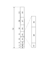
- FIG. 3 shows a configuration example of the field FLD for displaying an image of one screen.
- the length of one field FLD is 1/60 second (about 16.7 ms), and is composed of, for example, eight subfields SF (SF1-SF8).
- each subfield SF has a reset period RST, an address period ADR, and a sustain period SUS.
- the amounts of wall charges accumulated in the electrodes XE, YE, and AE are adjusted in order to match the discharge start voltages (voltages at which address discharge in the address period ADR starts to occur) of all cells. It is a period.
- the wall charges are, for example, plus charges and minus charges accumulated on the surface of the protective layer PL such as MgO shown in FIG. 2 in each cell.
- the address period ADR is a period for selecting a cell to be lit during the sustain period SUS.
- a cell to be lit in the sustain period SUS is selected by, for example, selectively generating an address discharge between the scan electrode YE and the address electrode AE in the address period as shown in FIG.
- the sustain period SUS is a period in which discharge (sustain discharge) is generated in the cell selected in the address period ADR.
- the length of the sustain period SUS varies depending on the subfield SF and depends on the number of discharges (luminance) of the cell. For this reason, it becomes possible to display an image with multiple gradations by changing the combination of the subfields SF to be lit.
- the number of discharge cycles preset in the subfields SF1 to SF8 is 4, 8, 16, 32, 64, 128, 256, and 512, respectively.
- the cell is discharged twice during one discharge cycle (star mark in the figure).
- FIG. 4 shows an outline of the circuit unit 60 shown in FIG.
- a capacitance Cax in the figure indicates a parasitic capacitance (interelectrode capacitance) formed between the address electrode AE and the sustain electrode XE, and a capacitance Cay is a parasitic capacitance (between electrodes) formed between the address electrode AE and the scan electrode YE. Capacity).
- the interelectrode capacitances Cax and Cay are collectively referred to as interelectrode capacitance Caxy.
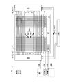
- the circuit unit 60 includes a voltage generation unit PWR, an X electrode driving unit XDR (sustain electrode driving unit), a Y electrode driving unit YDR (scanning electrode driving unit), an address electrode driving unit ADR, and a control unit CNT.
- the voltage generator PWR generates power supply voltages Vs / 2, ⁇ Vs / 2, Vsc, etc. to be supplied to the electrode drivers YDR and XDR.
- the electrode drive units XDR, YDR, and ADR operate as drive units that drive the PDP 10.
- the sustain electrode driver XDR applies a common pulse to the sustain electrode XE
- the scan electrode driver YDR selectively applies a pulse to the scan electrode YE
- the address electrode driver ADR applies to the address electrode AE.
- a pulse is selectively applied.
- the address electrode drive unit ADR includes a power cutoff unit PSI10 and an address driver AD (address electrode application unit, address voltage application unit) provided for each address electrode AE.
- the power shutoff unit PSI10 supplies the ground voltage to the address driver AD during the reset period RST and the address period ADR shown in FIG. 3 described above, and shuts off the ground voltage supplied to the address driver AD during the sustain period SUS.
- the address driver AD selectively applies an address pulse APL shown in FIG. 7 to be described later to the address electrode AE.
- the description of the power supply for supplying the power supply voltage to the address driver AD is omitted.
- the control unit CNT includes a driver control unit ADCN that generates a control signal ACNT (address control signal) for controlling the address driver AD, and a switch control unit SWCN that generates a control signal SCNT for controlling the power cutoff unit PSI10. have. Then, the control unit CNT selects a subfield to be used based on the image data R0-7, G0-7, B0-7, and outputs control signals YCNT, XCNT, and ACNT to the electrode drive units YDR, XDR, and ADR. . A multi-gradation image is displayed by selecting a subfield to be used for each cell constituting a pixel.
- the image data R0-7, G0-7, and B0-7 are 8-bit data for displaying red, green, and blue, respectively, and are sequentially sent from the tuner unit or external input (not shown) to the control unit CNT. Entered.
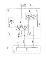
- FIG. 5 shows an example of the address electrode driver ADR shown in FIG.
- the interelectrode capacitance Caxy between the address electrode AEb, the sustain electrode XE, and the scan electrode YE is omitted.
- the voltage of the ground line GND is also referred to as a ground voltage GND.
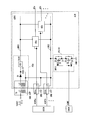
- the address electrode driver ADR includes an address driver AD (ADa, ADb) provided for each address electrode AE (AEa, AEb) and an isolator IS1 (IS1a, IS1b) provided for each address driver AD (ADa, ADb). And a power supply unit PS1 (internal power supply) and a power supply cutoff unit PSI10.
- a circuit group of the address electrode drive unit ADR (a circuit group including the address driver AD and the power supply unit PS1) excluding the power supply cutoff unit PSI10 is also referred to as an address drive circuit ADRC.
- the address driver AD includes a first transistor PM1 (PM1a, PM1b) and a second transistor NM1 (NM1a, NM1b) connected in series between the internal power supply line LN10 and the reference power supply line LN20.
- the common node ND1 (ND1a, ND1b) connecting the transistor PM1 and the transistor NM1 is connected to the address electrode AE (AEa, AEb).
- the transistor PM1 is a power pMOS transistor (P-channel FET) capable of flowing a large current, and has a parasitic diode whose anode is connected to the drain of the transistor PM1 and whose cathode is connected to the source of the transistor PM1.
- P-channel FET power pMOS transistor
- a threshold voltage between a drain and a gate to which an anode of a parasitic diode is connected is larger than a threshold voltage between a source and a gate to which a cathode of the parasitic diode is connected. Therefore, the power P-channel FET is turned on (off) based on the voltage between the source and the gate shown in the drawing.
- the transistor NM1 is a power nMOS transistor (N-channel FET) capable of flowing a large current, and has a parasitic diode whose anode is connected to the source of the transistor NM1 and whose cathode is connected to the drain of the transistor NM1. Yes.
- the threshold voltage between the drain and the gate to which the cathode of the parasitic diode is connected is larger than the threshold voltage between the source and the gate to which the anode of the parasitic diode is connected. Therefore, the power N-channel FET is turned on (off) based on the voltage between the source and the gate shown in the drawing.
- the source of the transistor PM1 is connected to the internal power supply line LN10, and the source of the transistor NM1 is connected to the reference power supply line LN20. That is, the cathode of the parasitic diode of the transistor PM1 is connected to the internal power supply line LN10, and the anode of the parasitic diode of the transistor NM1 is connected to the reference power supply line LN20. As a result, leakage current can be prevented from flowing from the internal power supply line LN10 to the reference power supply line LN20 via the parasitic diode.
- the gates of the transistors PM1 and NM1 are connected to each other and are connected to the driver control unit ADCN via the isolator IS1.
- the isolator IS1 includes a light emitting diode and a phototransistor, and maintains an galvanic isolation between the driver control unit ADCN and the address driver AD, and the address control signal ACNT (ACNTa) from the driver control unit ADCN to the address driver AD. , ACNTb).
- the isolator IS1 shifts the reference level of the address control signal ACNT from the ground voltage GND to the voltage of the reference power supply line LN20, and transmits the address control signal ACNT to the gates of the transistors PM1 and NM1.
- the logic level (H level and L level) of address control signal ACNT is reliably transmitted to transistors PM1 and NM1.
- the address control signal ACNT is at a high logic level (H level)
- the transistor PM1 is turned off
- the transistor NM1 is turned on
- the address control signal ACNT is at a low logic level (L level)
- the transistor PM1 is turned on. To do.
- the power supply unit PS1 is connected to the ground line GND via the reference power supply line LN20 and the power supply cutoff unit PSI10, and supplies the power supply voltage Vadd to the internal power supply line LN10 to which the transistor PM1 is connected. That is, the power supply unit PS1 maintains the voltage between the reference power supply line LN20 and the internal power supply line LN10 at the voltage Vadd.
- An example of the configuration of the power supply unit PS1 will be described later with reference to FIG.
- the power cutoff unit PSI10 has a switch SW10 disposed between the reference power supply line LN20 and the ground line GND. On / off of the switch SW10 is controlled by a control signal SCNT output from the switch control unit SWCN.
- the switch SW10 is configured such that no leakage current flows between the reference power supply line LN20 and the ground line GND when the switch SW10 is off.
- the switch SW10 is configured by an IGBT (Insulated Gate Bipolar Transistor) or a power MOS transistor.
- the IGBT is a bipolar transistor in which a MOSFET is incorporated in the gate.
- an IGBT does not have a parasitic diode between a collector and an emitter. For this reason, in the switch SW10 constituted by the IGBT, no leakage current flows between the reference power supply line LN20 and the ground line GND when the switch SW10 is off. Details of the switch SW10 formed of a power MOS transistor having a parasitic diode will be described later with reference to FIG.
- the switch SW10 is turned on to supply the ground voltage GND from the ground line GND to the reference power supply line LN20 in the address period ADR shown in FIG. That is, switch SW10 electrically connects address drive circuit ADRC having power supply unit PS1 and address driver AD and ground line GND in address period ADR.
- the ground voltage GND is supplied to the reference power supply line LN20
- the power supply voltage Vadd based on the ground voltage GND is supplied to the internal power supply line LN10.
- the transistor NM1 can apply the ground voltage GND to the address electrode AE when the address control signal ACNT is at a high logic level (H level).
- the transistor PM1 can apply the power supply voltage Vadd based on the ground voltage GND to the address electrode AE when the address control signal ACNT is at a low logic level (L level).
- the switch SW10 is turned off to bring the reference power supply line LN20 into a floating state during the sustain period SUS. That is, the switch SW10 electrically disconnects the address drive circuit ADRC and the ground line GND during the sustain period SUS. As described above, no leakage current flows between the reference power supply line LN20 and the ground line GND when the switch SW10 is off. Therefore, in this embodiment, it is possible to prevent a leak current from flowing between the address electrode AE and the ground line GND during the sustain period SUS.
- the sustain electrode XE and the scan electrode YE and the address electrode AE are connected via the interelectrode capacitance Caxy (the ground line GND-address electrode AE-interelectrode capacitance Caxy-sustain electrode XE).
- the interelectrode capacitance Caxy the ground line GND-address electrode AE-interelectrode capacitance Caxy-sustain electrode XE.
- FIG. 6 shows an example of the power supply unit PS1 and the switch SW10 shown in FIG.
- the power supply unit PS1 includes, for example, a part of the transformer T1 (coil L2), a rectifier circuit (diode D1 in the figure), a smoothing circuit (capacitor C1 in the figure), and a voltage stabilization circuit VS1.
- the transformer T1 has a configuration in which two coils L1 and L2 are coupled by a core, and the primary side (coil L1) and the secondary side (coil L2) are galvanically insulated, and one coil L1 is The applied change (AC voltage Vadd1 in the figure) is transmitted to the other coil L2.
- one terminal of the coil L1 is connected to the ground line GND, and the AC voltage Vadd1 is applied to the other terminal.
- the coil L2 has one terminal connected to the reference power line LN20 and the other terminal connected to the anode of the diode D1, and transmits a voltage change applied to the coil L1 to the diode D1.
- the cathode of the diode D1 is connected to one terminal of the capacitor C1 and the voltage stabilizing circuit VS1, and the other terminal of the capacitor C1 is connected to the reference power supply line LN20.
- a voltage rectified and smoothed with reference to the reference power supply line LN20 is supplied to the node where the diode D1 and the capacitor C1 are connected.
- the voltage stabilization circuit VS1 stabilizes the voltage rectified and smoothed with reference to the reference power supply line LN20 as the power supply voltage Vadd and supplies it to the internal power supply line LN10. Thereby, even when the reference power supply line LN20 is in a floating state, the power supply unit PS1 can maintain the voltage between the reference power supply line LN20 and the internal power supply line LN10 at the voltage Vadd.
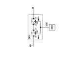
- the switch SW10 of the power shut-off unit PSI10 is composed of, for example, a pair of power nMOS transistors NM10 and NM20 (N channel FET) connected in series between the reference power supply line LN20 and the ground line GND.
- the common node that connects the gates of the transistors NM10 and NM20 to each other is connected to the switch control unit SWCN, and the control signal SCNT is received by the gate.
- the nMOS transistor NM10 has a drain connected to the reference power supply line LN20 and a source connected to the source of the nMOS transistor NM20.
- the nMOS transistor NM20 has a drain connected to the ground line GND. That is, the pair of power nMOS transistors NM10 and NM20 are connected in the direction in which the anodes of the parasitic diodes formed in the transistors NM10 and NM20 are connected to each other.
- the parasitic diode of the transistor NM10 prevents a leakage current from flowing from the reference power supply line LN20 to the ground line GND, and the parasitic diode of the transistor NM20 is connected from the ground line GND to the reference power supply line LN20. To prevent leakage current from flowing through.
- the switch SW10 transistors NM10 and NM20
- leakage current can be prevented from flowing between the reference power supply line LN20 and the ground line GND.
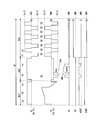
- FIG. 7 shows an example of the discharge operation of the subfield SF shown in FIG.
- the star in the figure indicates the occurrence of discharge.
- the shaded portion of the waveform of the address electrode AE in the figure indicates that the address electrode AE is in a floating state.
- the switch SW10 shown in FIG. 5 is turned on when receiving a control signal SCNT at a high logic level (H level) and turned off when receiving a control signal SCNT at a low logic level (L level). .
- a positive write voltage is applied to the sustain electrode XE (the bus electrode Xb and the transparent electrode Xt), and a positive write voltage is applied to the scan electrode YE (the bus electrode Yb and the transparent electrode Yt) ( FIG. 7 (a)).
- the sustain electrode XE is maintained at a positive write voltage, and a positive write voltage (write obtuse wave) that gradually increases is applied to the scan electrode YE (FIG. 7B).
- wall charges are accumulated in the sustain electrode XE, the scan electrode YE, and the address electrode AE, respectively, while suppressing the light emission of the cell.
- negative wall charges are accumulated in the sustain electrode XE and the scan electrode YE, respectively, and positive wall charges are accumulated in the address electrode AE.
- the sustain electrode XE is maintained at a positive write voltage, and a negative adjustment voltage (adjustment blunt wave) is applied to the scan electrode YE (FIG. 7C).
- a negative adjustment voltage adjustment blunt wave
- the positive adjustment voltage applied to the sustain electrode XE is a voltage lower than the voltage Vs / 2
- the minimum value of the negative adjustment voltage applied to the scan electrode YE is higher than the voltage ⁇ Vs / 2. It is a voltage (small voltage value as an absolute value).
- the ground voltage GND is supplied to the reference voltage line LN20 illustrated in FIG. 5 via the switch SW10. Since the control signal ACNT is maintained at the H level, the transistor PM1 shown in FIG. 5 is turned off, the transistor NM1 is turned on, and the transistor NM1 applies the ground voltage GND to the address electrode AE.
- the control signal SCNT is maintained at the H level by the switch control unit SWCN illustrated in FIG. 5, and the switch SW10 is maintained in the ON state.
- a bias voltage serving as an anode during address discharge is applied to the sustain electrode XE
- a scan pulse SPL (voltage ⁇ Vs / 2) serving as a cathode during address discharge is applied to the scan electrode YE, and during address discharge.
- An address pulse APL (voltage Vadd) serving as an anode is applied to the address electrode AE corresponding to the lighted cell (FIG. 7D).
- a discharge (address discharge) is temporarily generated between the scan electrode YE and the address electrode AE. Thereby, a cell to be lit in the sustain period SUS is selected.
- the transistor PM1 is turned on and the transistor NM1 is turned off. That is, when the address control signal ACNT is at the L level, the transistor PM1 applies the power supply voltage Vadd to the address electrode AE. In other words, the transistor PM1 applies the power supply voltage Vadd to the address electrode AE based on the address control signal ACNT.
- the transistor PM1 is turned off, the transistor NM1 is turned on, and the transistor NM1 applies the ground voltage GND to the address electrode AE. That is, the transistor NM1 applies the ground voltage GND to the address electrode AE based on the address control signal ACNT when the transistor PM1 in the address period ADR is off.
- the second address pulse APL shown in the waveform of the address electrode AE is applied to select a cell of another display line (FIG. 7E).
- the control signal SCNT is set to L level by the switch control unit SWCN shown in FIG. 5, and the switch SW10 is turned off. That is, in the sustain period SUS, as described above, the address drive circuit ADRC and the ground line GND are electrically disconnected. That is, in this embodiment, in the sustain period SUS, the address electrode AE can be in a floating (high impedance) state, and the average voltage of the sustain electrode XE and the scan electrode YE to which the sustain pulse is applied and the voltage of the address electrode AE The difference can be reduced.
- the displacement current (leakage current) between the sustain electrode XE, the scan electrode YE, and the address electrode AE generated by the difference between the average voltage of the sustain electrode XE and the scan electrode YE and the voltage of the address electrode AE can be reduced.
- the address control signal ACNT is maintained at the H level during the sustain period SUS. Note that, in the sustain period SUS, the address drive circuit ADRC and the ground line GND are not electrically connected, so the address control signal ACNT may be at the L level.
- the switch SW10 power cutoff unit PSI10
- the switch SW10 power cutoff unit PSI10 disposed between the reference power supply line LN20 and the ground line GND is turned off, and the ground voltage GND supplied to the reference power supply line LN20. Shut off. As a result, leakage current can be prevented from flowing between the reference power supply line LN20 and the ground line GND during the sustain period SUS, and power consumption can be reduced.
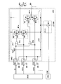
- FIG. 8 shows an address electrode driver ADR2 and a driver controller ADCN2 of a PDP device according to another embodiment.
- the address electrode drive unit ADR2 includes a 2-input OR circuit OR1 (OR1a, OR1b) added to the address electrode drive unit ADR shown in FIG. 5 described above, and the power cut-off unit PSI10 shown in FIG. Instead, a power cutoff unit PSI20 is provided.
- OR1a, OR1b 2-input OR circuit OR1
- the power supply unit PS1 and the isolator IS1 are omitted from the address electrode driver ADR shown in FIG.
- the other configuration of the address electrode driver ADR2 is the same as that in FIG.
- driver control unit ADCN2 of this embodiment is different from the driver control unit ADCN shown in FIG. 5 in that the address control signal SS is generated in addition to the address control signal ACNT.
- Other configurations of the driver control unit ADCN2 are the same as those in FIGS.
- the same elements as those described in FIGS. 1 to 7 are denoted by the same reference numerals, and detailed description thereof will be omitted.
- the source of the transistor NM1 (NM1a, NM1b) of the address driver AD (ADa, ADb) is connected to the ground line GND, and the source of the transistor PM1 (PM1a, PM1b) of the address driver AD (ADa, ADb) is a power cutoff unit
- the PSI 20 is connected to the first power supply line LN12.
- the power supply voltage Vadd is supplied to the first power supply line LN12 from the voltage generation unit PWR shown in FIG. 4 described above.
- the power cutoff unit PSI20 is configured by a power nMOS transistor NM30 having a source connected to the first power supply line LN12, a drain connected to the source of the transistor PM1, and a gate connected to the switch control unit SWCN. That is, in the transistor NM30, the anode of the parasitic diode of the transistor NM30 is connected to the first power supply line LN12, and the cathode of the parasitic diode is connected to the source of the transistor PM1, between the first power supply line LN12 and the transistor PM1. Placed in.
- the transistor NM30 is turned on during the reset period RST and the address period ADR shown in FIG. 3 described above, supplies the power supply voltage Vadd to the transistor PM1, turns off during the sustain period SUS, and cuts off the power supply voltage Vadd supplied to the transistor PM1. To do. That is, the transistor NM30 of the power cutoff unit PSI20 functions as a switch.
- the power cutoff unit PSI20 may be configured using a power pMOS transistor, IGBT, or the like instead of the power nMOS transistor NM30. In this case, the power pMOS transistor and the IGBT function as a switch.
- the two-input OR circuit OR1 receives the address control signal SS at one input terminal, receives the address control signal ACNT (ACNTa, ACNT1b) at the other input terminal, and receives the logic of the address control signals SS and ACNT. The sum is output to the gate of the transistor PM1 (PM1a, PM1b).
- An address control signal ACNT ACNTa, ACNT1b is supplied to the gate of the transistor NM1 (NM1a, NM1b).
- the driver control unit ADCN2 simultaneously turns off the transistors PM1 and NM1 by setting the address control signals SS and ACNT to the H level and the L level, respectively, during the sustain period SUS.
- a logic circuit for simultaneously turning off the transistors PM1 and NM1 may be configured by using a negative logical sum, a logical product, a negative logical product, or the like instead of the two-input logical sum circuit OR1.
- the two-input OR circuit OR1 may be provided in the driver control unit ADCN2.
- the address electrodes AE can be in a floating (high impedance) state by simultaneously turning off the transistors PM1 and NM1.
- the difference between the average voltage of the sustain electrode XE and the scan electrode YE to which the sustain pulse is applied and the voltage of the address electrode AE can be reduced, and the displacement current between the sustain electrode XE, the scan electrode YE, and the address electrode AE ( (Leakage current) can be reduced.
- the transistors PM1, NM1, and NM30 can be turned off, and the sustain electrode XE, the scan electrode YE, and the address electrode AE are connected via the interelectrode capacitance Caxy. It is possible to prevent leakage current from flowing between them. As a result, in this embodiment, power consumption can be reduced.
- FIG. 9 shows an example of the discharge operation of the subfield SF by the address electrode driver ADR2 shown in FIG. Detailed description of the same operations as those in FIG. 7 described above will be omitted.
- the waveform shown in FIG. 9 is different from FIG. 7 in that the waveform of the address control signal SS is added.
- Other waveforms are the same as those in FIG.
- the meanings of stars and shaded portions in the figure are the same as those in FIG.
- the address control signal SS is maintained at the L level.
- the transistor PM1 shown in FIG. 8 described above can apply the power supply voltage Vadd to the address electrode AE, and when the address control signal ACNT is at the H level, the transistor NM1 A ground voltage GND can be applied to the electrode AE.
- the address control signal SS is maintained at the H level, and the address control signal ACNT is maintained at the L level.
- the transistors PM1 and NM1 are turned off.
- the control signal SCNT is set to the L level, the transistor NM30 is turned off.
- the sustain electrode XE and the scan electrode YE are connected via the interelectrode capacitance Caxy as described above with reference to FIG. It is possible to prevent a leak current from flowing between the address electrode AE. As described above, also in this embodiment, power consumption can be reduced.
- FIG. 10 shows an address electrode drive unit ADR3 and a control unit CNT2 of a PDP device in another embodiment.
- the interelectrode capacitance Caxy between the address electrode AEb, the sustain electrode XE, and the scan electrode YE is omitted.
- the control unit CNT2 in the figure omits the description of the image data R0-7, G0-7, B0-7 and the control signals XCNT, YCNT.
- the address electrode driver ADR3 is provided with a power cutoff unit PSI22 instead of the power cutoff unit PSI20 shown in FIG.
- the other configuration of the address electrode driver ADR3 is the same as that in FIG.
- control unit CNT2 of this embodiment is configured by omitting the switch control unit SWCN from the control unit CNT shown in FIG. 4 described above. Further, the control unit CNT2 is provided with the driver control unit ADCN2 shown in FIG. 8 described above instead of the driver control unit ADCN shown in FIG. The other configuration of the control unit CNT2 is the same as that in FIG.
- the discharge operation of the subfield SF is the same as the waveform obtained by omitting the control signal SCNT from the waveform shown in FIG. That is, the waveforms of the electrodes XE, YE, AE and the control signals ACNT, SS are the same as those in FIG.
- the same elements as those described in FIGS. 1 to 9 are denoted by the same reference numerals, and detailed description thereof will be omitted.
- the power cutoff unit PSI22 is configured by a diode D10 having an anode connected to the first power supply line LN12 and a cathode connected to the source of the transistor PM1.
- the power supply voltage Vadd is supplied from the first power supply line LN12 to the transistor PM1 via the diode D10.
- a voltage that is lowered from the power supply voltage Vadd by the forward voltage of the diode D10 is supplied to the transistor PM1.
- the diode D10 cuts off the power supply voltage Vadd supplied to the transistor PM1 by turning off the transistor PM1 during the sustain period SUS shown in FIG. Further, the diode D10 prevents a leakage current from flowing from the address electrode AE to the first power supply line LN12 through the parasitic diode of the transistor PM1 when the transistor PM1 is turned off.
- the address control signals SS and ACNT are set to the H level and the L level, respectively, and the transistors PM1 and NM1 are turned off. Accordingly, the diode D10 can prevent a leak current from flowing from the address electrode AE to the first power supply line LN12 through the parasitic diode of the transistor PM1 during the sustain period SUS. In this case, since the transistor PM1 is off, it is possible to prevent a leak current from flowing from the first power supply line LN12 to the address electrode AE. Further, since the transistor NM1 is off, it is possible to prevent a leak current from flowing from the address electrode AE to the ground line GND.
- the leakage current flows between the sustain electrode XE, the scan electrode YE, and the address electrode AE through the interelectrode capacitance Caxy by turning off the transistors PM1 and NM1 during the sustain period SUS. Can be prevented.
- the same effect as that of the embodiment described with reference to FIGS. 8 and 9 can be obtained.
- FIG. 11 shows an address electrode driver ADR4, a driver controller ADCN, and a switch controller SWCN of a PDP device in another embodiment.
- the interelectrode capacitance Caxy between the address electrode AEb, the sustain electrode XE, and the scan electrode YE is omitted.
- the address electrode driver ADR4 is configured by adding switches SW20 (SW20a, SW20b) to the address electrode driver ADR shown in FIG.
- the power supply cutoff unit PSI10, the power supply unit PS1, and the isolator IS1 are omitted from the address electrode driver ADR shown in FIG.
- the other configuration of the address electrode driver ADR4 is the same as that in FIG.
- the configurations of the driver control unit ADCN and the switch control unit SWCN are the same as those in FIG. 5 except for the output destinations of the control signals ACNT and SCNT.
- the discharge operation of the subfield SF is the same as that in FIG.
- the same elements as those described in FIGS. 1 to 7 are denoted by the same reference numerals, and detailed description thereof will be omitted.
- the source of the transistor NM1 (NM1a, NM1b) of the address driver AD (ADa, ADb) is connected to the ground line GND
- the source of the transistor PM1 (PM1a, PM1b) of the address driver AD (ADa, ADb) is the internal power supply line Connected to LN10.
- the power supply voltage Vadd is supplied to the internal power supply line LN10 from the voltage generation unit PWR shown in FIG. 4 described above.
- the gates of the transistors PM1 and NM1 are connected to each other and to the driver control unit ADCN.
- the switch SW20 (SW20a, SW20b) is provided between the address driver AD (ADa, ADb) and the address electrode AE (AEa, AEb) for each address electrode AE (AEa, AEb).
- ON / OFF of the switch SW20 is controlled by a control signal SCNT output from the switch control unit SWCN.
- the switch SW20 is configured such that no leak current flows between the address driver AD and the address electrode AE when the switch SW20 is off. For example, by turning off the switch SW20 during the sustain period SUS, the current flowing from the transistor PM1 to the address electrode AE and the current flowing from the address electrode AE to the transistor NM1 are cut off.
- the switch SW10 is configured by an IGBT or a power MOS transistor.
- the IGBT does not have a parasitic diode between the collector and the emitter
- the switch SW20 configured by the IGBT when the switch SW20 is off, a leakage current is generated between the address driver AD and the address electrode AE. Does not flow. Details of the switch SW20 formed of a power MOS transistor having a parasitic diode will be described later with reference to FIG.
- the driver control unit ADCN turns off the switch SW20 by setting the control signal SCNT to the L level during the sustain period SUS.
- the switch SW20 when the switch SW20 is turned off, no leak current flows between the address driver AD and the address electrode AE. Therefore, in this embodiment, it is possible to prevent a leak current from flowing between the address electrode AE and the ground line GND and between the internal power supply line LN10 and the address electrode AE during the sustain period SUS.
- the switch SW20 by turning off the switch SW20 during the sustain period SUS, it is possible to prevent a leakage current from flowing between the sustain electrode XE, the scan electrode YE, and the address electrode AE via the interelectrode capacitance Caxy. . As a result, in this embodiment, power consumption can be reduced.
- the address control signal ACNT during the sustain period SUS since the switch SW20 is turned off during the sustain period SUS, the address control signal ACNT during the sustain period SUS may be H level or L level.
- FIG. 12 shows an example of the switch SW20 shown in FIG.
- the switch SW20 includes, for example, a pair of power nMOS transistors NM40 connected in series between the node ND1 (the common node ND1 connecting the transistor PM1 and the transistor NM1 shown in FIG. 11 described above) and the address electrode AE.
- NM50 N channel FET.
- a common node that connects the gates of the transistors NM40 and NM50 is connected to the switch control unit SWCN, and the control signal SCNT is received by the gate.
- the nMOS transistor NM40 has a drain connected to the node ND1 and a source connected to the source of the nMOS transistor NM50.
- the nMOS transistor NM50 has a drain connected to the address electrode AE. That is, the pair of power nMOS transistors NM40 and NM50 are connected in the direction in which the anodes of the parasitic diodes formed in the transistors NM40 and NM50 are connected to each other.
- the parasitic diode of the transistor NM40 prevents a leakage current from flowing from the node ND1 to the address electrode AE, and the parasitic diode of the transistor NM50 has a leakage current from the address electrode AE to the node ND1. Prevent it from flowing.
- the switch SW20 is off, it is possible to prevent a leak current from flowing between the node ND1 (the address driver AD shown in FIG. 11 described above) and the address electrode AE.
- the same effects as those of the embodiment described with reference to FIGS. 1 to 9 can be obtained.
- FIG. 13 shows an address electrode driver ADR5, a driver controller ADCN2, and a switch controller SWCN of a PDP device in another embodiment.
- the interelectrode capacitance Caxy between the address electrode AEb, the sustain electrode XE, and the scan electrode YE is omitted.
- the address electrode driver ADR5 is configured by adding a two-input OR circuit OR1 (OR1a, OR1b) and an isolator IS2 to the address electrode driver ADR shown in FIG.
- OR1a, OR1b OR1a, OR1b
- the other configuration of the address electrode driver ADR5 is the same as that in FIG.
- driver control unit ADCN2 of this embodiment is different from the driver control unit ADCN shown in FIG. 5 in that the address control signal SS is generated in addition to the address control signal ACNT.
- Other configurations of the driver control unit ADCN2 are the same as those in FIGS.
- the discharge operation of the subfield SF is the same as that in FIG.
- the same elements as those described in FIGS. 1 to 9 are denoted by the same reference numerals, and detailed description thereof will be omitted.
- one input terminal of the two-input OR circuit OR1 (OR1a, OR1b) is connected to the driver control unit ADCN2 via the isolator IS2, and the other input terminal is a driver via the isolator IS1 (IS1a, IS1b). It is connected to the control unit ADCN2.
- the output terminal of the 2-input OR circuit OR1 is connected to the gate of the transistor PM1 of the address driver AD.
- the 2-input OR circuit OR1 (OR1a, OR1b) outputs the logical sum of the address control signals SS and ACNT to the gate of the transistor PM1 (PM1a, PM1b).
- the gate of the transistor NM1 of the address driver AD is connected to one input terminal of a two-input OR circuit OR1 (OR1a, OR1b), and is connected to the driver control unit ADCN2 via the isolator IS1.
- the driver control unit ADCN2 simultaneously turns off the transistors PM1 and NM1 by setting the address control signals SS and ACNT to the H level and the L level, respectively, during the sustain period SUS.
- a logic circuit for simultaneously turning off the transistors PM1 and NM1 may be configured by using a negative logical sum, a logical product, a negative logical product, or the like instead of the two-input logical sum circuit OR1.
- the two-input OR circuit OR1 may be provided in the driver control unit ADCN2.
- the internal power supply line LN10 and the address electrode AE and the address electrode AE and the reference power supply line LN20 can be in a high impedance state.
- the difference between the average voltage of the sustain electrode XE and the scan electrode YE to which the sustain pulse is applied and the voltage of the address electrode AE can be reliably reduced, and the displacement between the sustain electrode XE, the scan electrode YE, and the address electrode AE
- the current (leakage current) can be reliably reduced.
- FIG. 14 shows an address electrode drive unit ADR6, a driver control unit ADCN3, and a switch control unit SWCN of a PDP device in another embodiment.
- the interelectrode capacitance Caxy between the address electrode AEb, the sustain electrode XE, and the scan electrode YE is omitted.
- the address electrode driver ADR6 is configured by omitting the two-input OR circuit OR1 (OR1a, OR1b) from the address electrode driver ADR2 shown in FIG.
- OR1a, OR1b OR circuit OR1 (OR1a, OR1b) from the address electrode driver ADR2 shown in FIG.
- the configuration of the power cutoff unit PSI20 of the address electrode driver ADR6 is provided with a switch SW30 instead of the transistor NM30 shown in FIG.
- the other configuration of the address electrode driver ADR6 is the same as that in FIG.
- driver control unit ADCN3 of this embodiment is different from the driver control unit ADCN2 shown in FIG. 8 in that the address control signal SS shown in FIG. 8 is not generated.
- Other configurations of the driver control unit ADCN3 are the same as those in FIG.
- the same elements as those described in FIGS. 1 to 9 are denoted by the same reference numerals, and detailed description thereof will be omitted.
- the power shut-off unit PSI20 is configured by a switch SW30 that is turned on during the reset period RST and the address period ADR shown in FIG. 3 and turned off during the sustain period SUS.
- the switch SW30 the leakage current does not flow between the first power supply line LN12 and the transistor PM1 when the switch SW30 is turned off by the IGBT or the pair of power nMOS transistors shown in FIGS. 6 and 12 described above. Configured as follows.
- the gates of the transistors PM1 and NM1 are connected to each other and to the driver control unit ADCN3.
- the driver control unit ADCN3 turns off the transistor NM1 by setting the address control signal ACNT to the L level during the sustain period SUS.
- the transistor NM1 it is possible to prevent a leak current from flowing between the address electrode AE and the reference power supply line LN20.
- the switch SW30 since the switch SW30 is turned off during the sustain period SUS, it is possible to prevent a leak current from flowing between the first power supply line LN12 and the transistor PM1. That is, in this embodiment, by turning off the switch SW30 and the transistor NM1 during the sustain period SUS, a leakage current flows between the sustain electrode XE, the scan electrode YE, and the address electrode AE via the interelectrode capacitance Caxy. Can be prevented. As a result, power consumption can be reduced.
- FIG. 15 shows an example of the discharge operation of the subfield SF by the address electrode driver ADR6 shown in FIG. Detailed description of the same operations as those in FIG. 9 described above will be omitted.
- the waveform shown in FIG. 15 is different from FIG. 9 in that the waveform of the address control signal SS is omitted.
- Other waveforms are the same as those in FIG.
- the meanings of stars and shaded parts in the figure are the same as those in FIG.
- the control signal SCNT is maintained at the H level.
- the transistor PM1 shown in FIG. 14 described above can apply the power supply voltage Vadd to the address electrode AE, and when the address control signal ACNT is at the H level, the transistor NM1 A ground voltage GND can be applied to the electrode AE.
- the address control signal ACNT and the control signal SCNT are set to L level, respectively, and the transistor NM1 and the switch SW30 are turned off.
- the switch SW30 is configured such that no leakage current flows between the first power supply line LN12 and the transistor PM1 when the switch SW30 is turned off. For this reason, in the sustain period SUS, it is possible to prevent a leak current from flowing between the first power supply line LN12 and the transistor PM1 even if the transistor PM is turned on.
- one pixel includes three cells (red (R), green (G), and blue (B)) has been described.
- the present invention is not limited to such an embodiment.
- one pixel may be composed of four or more cells.
- one pixel may be composed of cells that generate colors other than red (R), green (G), and blue (B), and one pixel may be red (R), green (G), Cells that generate colors other than blue (B) may be included.
- the second direction D2 may intersect the first direction D1 in a substantially perpendicular direction (for example, 90 ° ⁇ 5 °). Also in this case, the same effect as the above-described embodiment can be obtained.
- the present invention is not limited to such an embodiment.
- the ground voltage GND and the voltage Vs may be alternately applied to the sustain electrode XE and the scan electrode YE during the sustain period SUS.
- the address electrode AE can be prevented from becoming lower than the ground voltage GND during the sustain period SUS.
- the address driver AD is configured by the pMOS transistor PM1 and the nMOS transistor NM1 .
- the address driver AD may be composed of a PNP bipolar transistor and an NPN bipolar transistor instead of the pMOS transistor PM1 and the nMOS transistor NM1.
- the address driver AD may be configured using an nMOS transistor NM2 instead of the pMOS transistor PM1.
- the gate of the nMOS transistor NM2 receives, for example, a control signal whose logic level (high logic and low logic) is opposite to the control signal received by the gate of the pMOS transistor PM1 shown in FIG.
- FIG. 16 shows a modification of the address electrode driver ADR shown in FIGS. 5 and 6 described above.
- the address electrode driver ADR7 shown in FIG. 16 is provided with an address driver AD2 (AD2a) instead of the address driver AD shown in FIG.
- a power supply unit PS2 (PS2a), an inverter INV1 (INV1a), and a level shifter LS1 (LS1a) provided for each address driver AD2 are added to the address electrode driver ADR shown in FIG. Configured.
- PS2a power supply unit PS2
- INV1a inverter INV1
- LS1a level shifter LS1
- a circuit group (a circuit group including the address driver AD2 and the power supply unit PS1) of the address electrode drive unit ADR7 excluding the power supply cutoff unit PSI10 is also referred to as an address drive circuit ADRC3.
- the transistor NM2 of the address driver AD2 has a source connected to the node ND1 (address electrode AE and the drain of the transistor NM1), a drain connected to the internal power supply line LN10, and a gate connected to the output of the inverter INV1. That is, the cathode of the parasitic diode of the transistor NM2 is connected to the internal power supply line LN10, and the anode of the parasitic diode of the transistor NM2 is connected to the node ND1. As a result, leakage current can be prevented from flowing from the internal power supply line LN10 to the reference power supply line LN20 via the parasitic diode.
- the configuration of the power supply unit PS2 (PS2a) is the same as that of the power supply unit PS1 except that the coil L2 and the capacitor C1 are connected to the node ND1 (ND1a).
- the power supply unit PS2 Based on the AC voltage Vadd2 applied to the coil L1 of the transformer T1 of the power supply unit PS2, the power supply unit PS2 generates the power supply voltage Vadd3 using the voltage of the node ND1 as a reference (minimum voltage).
- the power supply voltage Vadd3 is supplied to the inverter INV1 as the power supply voltage of the inverter INV1.
- the voltage Vadd3 is a voltage higher than the threshold voltage of the transistor NM2.
- the voltage of the node ND1 is supplied to the inverter INV1 as the reference voltage (minimum voltage) of the inverter INV1.
- the transformer T1 of the power supply unit PS1 and the transformer T1 of the power supply unit PS2 may be configured to share the coil L1.
- the input terminal of the inverter INV1 is connected to the driver control unit ADCN via the level shifter LS1 and the isolator IS1.
- the level shifter LS1 is a circuit that shifts the input (output of the isolator IS1) signal to a level that matches the input range of the inverter INV1, and outputs the shifted signal to the inverter INV1.
- the inverter INV1 can output a voltage higher than the voltage of the node ND1 by the voltage Vadd3 to the transistor NM2 when the address control signal ACNT is at the L level. At this time, the transistor NM2 is turned on because the voltage Vadd3 larger than the threshold voltage is applied between the gate and the source. Further, regardless of the state of the reference power supply line LN20, the inverter INV1 can output the voltage of the node ND1 to L level and output it to the transistor NM2 when the address control signal ACNT is at H level. At this time, the transistor NM2 is turned off because a voltage (0 V) smaller than the threshold voltage is applied between the gate and the source.
- the gate of the transistor NM1 of the address driver AD2 is connected to the level shifter LS1 and to the driver control unit ADCN via the isolator IS1. Therefore, even in the configuration of FIG. 16, the discharge operation of subfield SF can be made the same as in FIG.
- the address drive circuit ADRC3 and the ground line GND can be electrically disconnected by setting the control signal SCNT to the L level during the sustain period SUS.
- the address driver AD2 is configured by the nMOS transistors NM1 and NM2, it is possible to obtain the same effect as that of the embodiment described with reference to FIGS. In the embodiment described with reference to FIG. 8 to FIG. 15, even when the address driver AD2 is used instead of the address driver AD, the same effect as that of the embodiment described with reference to FIG. 8 to FIG. Can be obtained.
- the present invention can be applied to a plasma display device and a method for controlling the plasma display device.
Landscapes
- Engineering & Computer Science (AREA)
- Physics & Mathematics (AREA)
- Power Engineering (AREA)
- Plasma & Fusion (AREA)
- Computer Hardware Design (AREA)
- General Physics & Mathematics (AREA)
- Theoretical Computer Science (AREA)
- Control Of Indicators Other Than Cathode Ray Tubes (AREA)
Abstract
La présente invention concerne une unité d'écran plasma comportant un écran d'affichage plasma (PDP) comprenant un premier substrat et un second substrat se faisant face via un espace de décharge, et une section de commande pour la commande de l'écran plasma PDP. Le premier substrat comporte une électrode de maintien (XE), une électrode de balayage (YE), et une électrode d'adresse (AE). La section de commande comporte une section d'application de tension d'électrode d'adresse (ADRC) comprenant un premier transistor (PM1) pour l'application de la tension d'alimentation (Vadd) à l'électrode d'adresse (AE) en fonction du signal de commande d'adresse (ACNT) lors d'une période d'adressage et un second transistor (NM1) pour l'application de la tension de terre (GND) à l'électrode d'adresse (AE) lorsque le premier transistor (PM1) est mis hors tension lors de la période d'adressage. La section de commande comporte également une section d'interruption d'alimentation (PS110) pour interrompre la tension de terre (GND) à alimenter à la section d'application de tension d'électrode d'adresse (ADRC) lors d'une période de d'entretien, permettant ainsi la réduction de la consommation d'énergie.
Priority Applications (1)
| Application Number | Priority Date | Filing Date | Title |
|---|---|---|---|
| PCT/JP2008/000083 WO2009093285A1 (fr) | 2008-01-24 | 2008-01-24 | Unité d'écran plasma et son procédé de commande |
Applications Claiming Priority (1)
| Application Number | Priority Date | Filing Date | Title |
|---|---|---|---|
| PCT/JP2008/000083 WO2009093285A1 (fr) | 2008-01-24 | 2008-01-24 | Unité d'écran plasma et son procédé de commande |
Publications (1)
| Publication Number | Publication Date |
|---|---|
| WO2009093285A1 true WO2009093285A1 (fr) | 2009-07-30 |
Family
ID=40900806
Family Applications (1)
| Application Number | Title | Priority Date | Filing Date |
|---|---|---|---|
| PCT/JP2008/000083 Ceased WO2009093285A1 (fr) | 2008-01-24 | 2008-01-24 | Unité d'écran plasma et son procédé de commande |
Country Status (1)
| Country | Link |
|---|---|
| WO (1) | WO2009093285A1 (fr) |
Cited By (1)
| Publication number | Priority date | Publication date | Assignee | Title |
|---|---|---|---|---|
| JP2013025474A (ja) * | 2011-07-19 | 2013-02-04 | Asahi Kasei Electronics Co Ltd | 接続機器の検出回路 |
Citations (8)
| Publication number | Priority date | Publication date | Assignee | Title |
|---|---|---|---|---|
| JPS5778751A (en) * | 1980-10-31 | 1982-05-17 | Fujitsu Ltd | Gas discharge panel |
| JPH0297113A (ja) * | 1988-10-03 | 1990-04-09 | Toshiba Corp | ソリッド・ステート・リレー |
| JPH06130914A (ja) * | 1992-06-09 | 1994-05-13 | Nec Corp | プラズマディスプレイの駆動装置 |
| JPH06216736A (ja) * | 1993-01-14 | 1994-08-05 | Matsushita Electric Works Ltd | バリスタを備える固体リレー |
| JPH08123362A (ja) * | 1994-10-28 | 1996-05-17 | Noritake Co Ltd | プラズマディスプレイパネルの駆動方法 |
| US6376995B1 (en) * | 1998-12-25 | 2002-04-23 | Matsushita Electric Industrial Co., Ltd. | Plasma display panel, display apparatus using the same and driving method thereof |
| JP2004273265A (ja) * | 2003-03-07 | 2004-09-30 | Fujitsu Hitachi Plasma Display Ltd | プラズマディスプレイパネル |
| JP2006323362A (ja) * | 2005-05-17 | 2006-11-30 | Lg Electronics Inc | プラズマディスプレイ装置、その駆動方法、及びプラズマディスプレイパネル |
-
2008
- 2008-01-24 WO PCT/JP2008/000083 patent/WO2009093285A1/fr not_active Ceased
Patent Citations (8)
| Publication number | Priority date | Publication date | Assignee | Title |
|---|---|---|---|---|
| JPS5778751A (en) * | 1980-10-31 | 1982-05-17 | Fujitsu Ltd | Gas discharge panel |
| JPH0297113A (ja) * | 1988-10-03 | 1990-04-09 | Toshiba Corp | ソリッド・ステート・リレー |
| JPH06130914A (ja) * | 1992-06-09 | 1994-05-13 | Nec Corp | プラズマディスプレイの駆動装置 |
| JPH06216736A (ja) * | 1993-01-14 | 1994-08-05 | Matsushita Electric Works Ltd | バリスタを備える固体リレー |
| JPH08123362A (ja) * | 1994-10-28 | 1996-05-17 | Noritake Co Ltd | プラズマディスプレイパネルの駆動方法 |
| US6376995B1 (en) * | 1998-12-25 | 2002-04-23 | Matsushita Electric Industrial Co., Ltd. | Plasma display panel, display apparatus using the same and driving method thereof |
| JP2004273265A (ja) * | 2003-03-07 | 2004-09-30 | Fujitsu Hitachi Plasma Display Ltd | プラズマディスプレイパネル |
| JP2006323362A (ja) * | 2005-05-17 | 2006-11-30 | Lg Electronics Inc | プラズマディスプレイ装置、その駆動方法、及びプラズマディスプレイパネル |
Cited By (1)
| Publication number | Priority date | Publication date | Assignee | Title |
|---|---|---|---|---|
| JP2013025474A (ja) * | 2011-07-19 | 2013-02-04 | Asahi Kasei Electronics Co Ltd | 接続機器の検出回路 |
Similar Documents
| Publication | Publication Date | Title |
|---|---|---|
| WO1998044531A1 (fr) | Panneau d'affichage plan, son procede de fabrication, organe de commande destine a agir dessus et procede de commande de ce panneau | |
| KR100639540B1 (ko) | 플라즈마 디스플레이 패널 구동 방법, 플라즈마 디스플레이 패널 구동 회로, 및 플라즈마 디스플레이 장치 | |
| JPH07295506A (ja) | プラズマディスプレイパネルの駆動方法 | |
| JP4496703B2 (ja) | プラズマディスプレイパネルの駆動方法 | |
| WO2009093285A1 (fr) | Unité d'écran plasma et son procédé de commande | |
| WO2002086854A1 (fr) | Procede de commande de panneau d'affichage au plasma et dispositif d'affichage au plasma | |
| EP1693821A2 (fr) | Appareil d'affichage à plasma et son procédé de commande | |
| JP2005250489A (ja) | プラズマディスプレイパネルの駆動装置及び駆動方法 | |
| KR100333414B1 (ko) | 플라즈마 어드레스 일렉트로루미네센스 표시장치 및 그 구동방법 | |
| JPWO2007023744A1 (ja) | プラズマディスプレイパネル駆動回路およびプラズマディスプレイ装置 | |
| JP2005338842A (ja) | プラズマディスプレイ装置 | |
| US8081143B2 (en) | Plasma display apparatus | |
| KR20020085026A (ko) | 플라즈마 디스플레이 패널의 구동방법 및 데이터 구동장치 | |
| JP2006317811A (ja) | プラズマ表示装置及び該プラズマ表示装置に用いられる駆動方法 | |
| JP2005189848A (ja) | プラズマディスプレイパネルの駆動方法、プラズマディスプレイパネルの駆動回路、及びプラズマ表示装置 | |
| KR100264452B1 (ko) | 3전극 면방전 플라즈마 디스플레이 패널의 구동방법 및 그 구동회로 | |
| KR100325301B1 (ko) | 플라즈마디스플레이패널(pdp) | |
| JP2565074B2 (ja) | プラズマ表示パネル駆動回路 | |
| JP5150632B2 (ja) | プラズマディスプレイパネルの駆動方法およびプラズマディスプレイ装置 | |
| US20080061704A1 (en) | Plasma Display Device | |
| JP2012018392A (ja) | プラズマディスプレイ装置の駆動方法およびプラズマディスプレイ装置 | |
| JP2001306027A (ja) | プラズマディスプレイパネルの駆動方法 | |
| JP2011257620A (ja) | プラズマディスプレイ装置の駆動方法およびプラズマディスプレイ装置 | |
| KR20060082987A (ko) | 디스플레이 장치 및 그의 전력 제어 방법 | |
| JP2005100869A (ja) | プラズマ表示装置及びその駆動方法 |
Legal Events
| Date | Code | Title | Description |
|---|---|---|---|
| 121 | Ep: the epo has been informed by wipo that ep was designated in this application |
Ref document number: 08702824 Country of ref document: EP Kind code of ref document: A1 |
|
| NENP | Non-entry into the national phase |
Ref country code: DE |
|
| 122 | Ep: pct application non-entry in european phase |
Ref document number: 08702824 Country of ref document: EP Kind code of ref document: A1 |
|
| NENP | Non-entry into the national phase |
Ref country code: JP |