WO2009093459A1 - Appareil de développement de couche atomique et procédé de formation de film mince - Google Patents
Appareil de développement de couche atomique et procédé de formation de film mince Download PDFInfo
- Publication number
- WO2009093459A1 WO2009093459A1 PCT/JP2009/000240 JP2009000240W WO2009093459A1 WO 2009093459 A1 WO2009093459 A1 WO 2009093459A1 JP 2009000240 W JP2009000240 W JP 2009000240W WO 2009093459 A1 WO2009093459 A1 WO 2009093459A1
- Authority
- WO
- WIPO (PCT)
- Prior art keywords
- substrate
- gas
- film
- film formation
- substrate stage
- Prior art date
- Legal status (The legal status is an assumption and is not a legal conclusion. Google has not performed a legal analysis and makes no representation as to the accuracy of the status listed.)
- Ceased
Links
Images






Classifications
-
- C—CHEMISTRY; METALLURGY
- C23—COATING METALLIC MATERIAL; COATING MATERIAL WITH METALLIC MATERIAL; CHEMICAL SURFACE TREATMENT; DIFFUSION TREATMENT OF METALLIC MATERIAL; COATING BY VACUUM EVAPORATION, BY SPUTTERING, BY ION IMPLANTATION OR BY CHEMICAL VAPOUR DEPOSITION, IN GENERAL; INHIBITING CORROSION OF METALLIC MATERIAL OR INCRUSTATION IN GENERAL
- C23C—COATING METALLIC MATERIAL; COATING MATERIAL WITH METALLIC MATERIAL; SURFACE TREATMENT OF METALLIC MATERIAL BY DIFFUSION INTO THE SURFACE, BY CHEMICAL CONVERSION OR SUBSTITUTION; COATING BY VACUUM EVAPORATION, BY SPUTTERING, BY ION IMPLANTATION OR BY CHEMICAL VAPOUR DEPOSITION, IN GENERAL
- C23C16/00—Chemical coating by decomposition of gaseous compounds, without leaving reaction products of surface material in the coating, i.e. chemical vapour deposition [CVD] processes
- C23C16/22—Chemical coating by decomposition of gaseous compounds, without leaving reaction products of surface material in the coating, i.e. chemical vapour deposition [CVD] processes characterised by the deposition of inorganic material, other than metallic material
- C23C16/30—Deposition of compounds, mixtures or solid solutions, e.g. borides, carbides, nitrides
- C23C16/40—Oxides
- C23C16/403—Oxides of aluminium, magnesium or beryllium
-
- C—CHEMISTRY; METALLURGY
- C23—COATING METALLIC MATERIAL; COATING MATERIAL WITH METALLIC MATERIAL; CHEMICAL SURFACE TREATMENT; DIFFUSION TREATMENT OF METALLIC MATERIAL; COATING BY VACUUM EVAPORATION, BY SPUTTERING, BY ION IMPLANTATION OR BY CHEMICAL VAPOUR DEPOSITION, IN GENERAL; INHIBITING CORROSION OF METALLIC MATERIAL OR INCRUSTATION IN GENERAL
- C23C—COATING METALLIC MATERIAL; COATING MATERIAL WITH METALLIC MATERIAL; SURFACE TREATMENT OF METALLIC MATERIAL BY DIFFUSION INTO THE SURFACE, BY CHEMICAL CONVERSION OR SUBSTITUTION; COATING BY VACUUM EVAPORATION, BY SPUTTERING, BY ION IMPLANTATION OR BY CHEMICAL VAPOUR DEPOSITION, IN GENERAL
- C23C16/00—Chemical coating by decomposition of gaseous compounds, without leaving reaction products of surface material in the coating, i.e. chemical vapour deposition [CVD] processes
- C23C16/44—Chemical coating by decomposition of gaseous compounds, without leaving reaction products of surface material in the coating, i.e. chemical vapour deposition [CVD] processes characterised by the method of coating
- C23C16/455—Chemical coating by decomposition of gaseous compounds, without leaving reaction products of surface material in the coating, i.e. chemical vapour deposition [CVD] processes characterised by the method of coating characterised by the method used for introducing gases into reaction chamber or for modifying gas flows in reaction chamber
- C23C16/45523—Pulsed gas flow or change of composition over time
- C23C16/45525—Atomic layer deposition [ALD]
- C23C16/45527—Atomic layer deposition [ALD] characterized by the ALD cycle, e.g. different flows or temperatures during half-reactions, unusual pulsing sequence, use of precursor mixtures or auxiliary reactants or activations
- C23C16/45536—Use of plasma, radiation or electromagnetic fields
-
- H—ELECTRICITY
- H01—ELECTRIC ELEMENTS
- H01J—ELECTRIC DISCHARGE TUBES OR DISCHARGE LAMPS
- H01J37/00—Discharge tubes with provision for introducing objects or material to be exposed to the discharge, e.g. for the purpose of examination or processing thereof
- H01J37/32—Gas-filled discharge tubes
- H01J37/32009—Arrangements for generation of plasma specially adapted for examination or treatment of objects, e.g. plasma sources
- H01J37/32082—Radio frequency generated discharge
- H01J37/321—Radio frequency generated discharge the radio frequency energy being inductively coupled to the plasma
-
- H—ELECTRICITY
- H01—ELECTRIC ELEMENTS
- H01J—ELECTRIC DISCHARGE TUBES OR DISCHARGE LAMPS
- H01J37/00—Discharge tubes with provision for introducing objects or material to be exposed to the discharge, e.g. for the purpose of examination or processing thereof
- H01J37/32—Gas-filled discharge tubes
- H01J37/32009—Arrangements for generation of plasma specially adapted for examination or treatment of objects, e.g. plasma sources
- H01J37/32082—Radio frequency generated discharge
- H01J37/321—Radio frequency generated discharge the radio frequency energy being inductively coupled to the plasma
- H01J37/3211—Antennas, e.g. particular shapes of coils
-
- H—ELECTRICITY
- H10—SEMICONDUCTOR DEVICES; ELECTRIC SOLID-STATE DEVICES NOT OTHERWISE PROVIDED FOR
- H10P—GENERIC PROCESSES OR APPARATUS FOR THE MANUFACTURE OR TREATMENT OF DEVICES COVERED BY CLASS H10
- H10P14/00—Formation of materials, e.g. in the shape of layers or pillars
- H10P14/60—Formation of materials, e.g. in the shape of layers or pillars of insulating materials
- H10P14/63—Formation of materials, e.g. in the shape of layers or pillars of insulating materials characterised by the formation processes
- H10P14/6326—Deposition processes
- H10P14/6328—Deposition from the gas or vapour phase
- H10P14/6334—Deposition from the gas or vapour phase using decomposition or reaction of gaseous or vapour phase compounds, i.e. chemical vapour deposition
- H10P14/6336—Deposition from the gas or vapour phase using decomposition or reaction of gaseous or vapour phase compounds, i.e. chemical vapour deposition in the presence of a plasma [PECVD]
-
- H—ELECTRICITY
- H10—SEMICONDUCTOR DEVICES; ELECTRIC SOLID-STATE DEVICES NOT OTHERWISE PROVIDED FOR
- H10P—GENERIC PROCESSES OR APPARATUS FOR THE MANUFACTURE OR TREATMENT OF DEVICES COVERED BY CLASS H10
- H10P14/00—Formation of materials, e.g. in the shape of layers or pillars
- H10P14/60—Formation of materials, e.g. in the shape of layers or pillars of insulating materials
- H10P14/63—Formation of materials, e.g. in the shape of layers or pillars of insulating materials characterised by the formation processes
- H10P14/6326—Deposition processes
- H10P14/6328—Deposition from the gas or vapour phase
- H10P14/6334—Deposition from the gas or vapour phase using decomposition or reaction of gaseous or vapour phase compounds, i.e. chemical vapour deposition
- H10P14/6339—Deposition from the gas or vapour phase using decomposition or reaction of gaseous or vapour phase compounds, i.e. chemical vapour deposition deposition by cyclic CVD, e.g. ALD, ALE or pulsed CVD
-
- H—ELECTRICITY
- H10—SEMICONDUCTOR DEVICES; ELECTRIC SOLID-STATE DEVICES NOT OTHERWISE PROVIDED FOR
- H10P—GENERIC PROCESSES OR APPARATUS FOR THE MANUFACTURE OR TREATMENT OF DEVICES COVERED BY CLASS H10
- H10P14/00—Formation of materials, e.g. in the shape of layers or pillars
- H10P14/60—Formation of materials, e.g. in the shape of layers or pillars of insulating materials
- H10P14/66—Formation of materials, e.g. in the shape of layers or pillars of insulating materials characterised by the type of materials
- H10P14/668—Formation of materials, e.g. in the shape of layers or pillars of insulating materials characterised by the type of materials the materials being characterised by the deposition precursor materials
-
- H—ELECTRICITY
- H10—SEMICONDUCTOR DEVICES; ELECTRIC SOLID-STATE DEVICES NOT OTHERWISE PROVIDED FOR
- H10P—GENERIC PROCESSES OR APPARATUS FOR THE MANUFACTURE OR TREATMENT OF DEVICES COVERED BY CLASS H10
- H10P14/00—Formation of materials, e.g. in the shape of layers or pillars
- H10P14/60—Formation of materials, e.g. in the shape of layers or pillars of insulating materials
- H10P14/69—Inorganic materials
- H10P14/692—Inorganic materials composed of oxides, glassy oxides or oxide-based glasses
- H10P14/6938—Inorganic materials composed of oxides, glassy oxides or oxide-based glasses the material containing at least one metal element, e.g. metal oxides, metal oxynitrides or metal oxycarbides
- H10P14/6939—Inorganic materials composed of oxides, glassy oxides or oxide-based glasses the material containing at least one metal element, e.g. metal oxides, metal oxynitrides or metal oxycarbides characterised by the metal
- H10P14/69391—Inorganic materials composed of oxides, glassy oxides or oxide-based glasses the material containing at least one metal element, e.g. metal oxides, metal oxynitrides or metal oxycarbides characterised by the metal the material containing aluminium, e.g. Al2O3
Definitions
- the present invention relates to atomic layer growth (hereinafter abbreviated as ALD (Atomic Layer)) in which a thin film is formed on a substrate in atomic layer units.
- ALD atomic layer growth
- This also relates to an apparatus and a thin film forming method.
- the ALD method two types of gas mainly composed of elements constituting a film to be formed are alternately supplied onto a film formation target substrate, and a thin film is formed on the substrate in units of atomic layers repeatedly several times.
- This is a thin film forming technique for forming a film having a desired thickness.
- a source gas containing Si and an oxidizing gas containing O are used.
- a nitriding gas is used instead of the oxidizing gas.
- the ALD method has a high step coverage and film thickness controllability compared to a general CVD (Chemical Vapor Deposition) method, and can be used to form capacitors for memory elements and insulating films called “high-k gates”. Practical use is expected.
- an insulating film can be formed at a low temperature of about 300 ° C., application to formation of a gate insulating film of a thin film transistor of a display device using a glass substrate such as a liquid crystal display is expected.
- FIG. 7 is a schematic diagram showing an example of the configuration of a conventional ALD apparatus.
- the ALD apparatus 50 shown in FIG. 1 includes a film forming container (film forming chamber) 12, a gas supply unit 14, and an exhaust unit 16.
- the film formation container 12 has a metal hollow box shape and is grounded. Inside the film forming container 12, an antenna array 28 including a plurality of antenna elements 26 and a substrate stage 32 incorporating a heater 30 are arranged in order from the upper wall side to the lower wall side. In the antenna array 28, a virtual plane constituted by arranging a plurality of antenna elements 26 in parallel at a predetermined interval is arranged in parallel with the substrate stage 32.
- the antenna element 26 is a rod-shaped monopole made of a conductor having a length of (2n + 1) / 4 times the wavelength of high-frequency power (n is 0 or a positive integer).
- An antenna (antenna body) 39 is housed in a cylindrical member 40 made of a dielectric.
- Each antenna element 26 is proposed by the present applicant in Japanese Patent Application Laid-Open No. 2003-86581.
- each antenna element 26 is orthogonal to the gas flow direction of the oxidizing gas supplied from the supply hole 20b toward the substrate stage 32.
- the film forming vessel 12 is attached to the side wall of the film forming container 12 so as to extend in the direction of the film.
- the antenna elements 26 are arranged in parallel at a predetermined interval, and the feeding positions of the adjacent antenna elements 26 are arranged so as to be located on the side walls facing each other. Yes.
- the substrate 42 is placed on the upper surface of the substrate stage 32.
- the substrate stage 32 is heated by the heater 30, and the substrate 42 placed on the substrate stage 32 is held at a predetermined temperature until film formation is completed.
- the source gas containing Si component is supplied from the gas supply unit 14 to the supply pipe 18a,
- the film is supplied in the horizontal direction into the film forming chamber 48 through a supply hole 20 a formed in the left wall of the film forming container 12.
- the source gas is supplied to the surface of the substrate 42 and the source gas component is adsorbed. At this time, no plasma is generated by the antenna element 26.
- the supply of the source gas is stopped, and an excess source gas other than the source gas component adsorbed on the surface of the substrate 42 is formed from the film formation container 12 to the right wall of the film formation container 12 by the exhaust unit 16.
- the air is exhausted horizontally through the exhaust holes 24 and the exhaust pipe 22.
- the oxidizing gas is supplied from the gas supply unit 14 in the horizontal direction into the film forming container 12 through the supply pipe 18 b and the supply hole 20 b formed in the left wall of the film forming container 12.
- high frequency power is supplied from the high frequency power supply unit 34 to each antenna element 26.
- plasma is generated around each antenna element 26 using an oxidizing gas, and the source gas component adsorbed on the surface of the substrate 42 is oxidized.
- the SiO 2 film is formed on the substrate 42 in units of atomic layers by a series of steps including supply of source gas ⁇ exhaust of excess source gas ⁇ supply of oxidizing gas ⁇ exhaust of excess oxidizing gas. By repeating this process several times, a SiO 2 film having a predetermined thickness is formed on the substrate 42.
- CCP Capacitive-Coupled Plasma
- IPC Inductively Coupled Plasma
- ECR Electro-Cyclotron Resonance Plasma
- the pressure of the raw material gas is generally set to a low pressure such as 10 Pa or less. Accordingly, there is a problem that it is difficult to stably generate plasma in the ALD method film formation in which the gas pressure is several Pa or more by the source gas supplied in a pulse form.
- CCP is not limited by gas pressure, but has a problem that plasma density is essentially low.
- the antenna array 28 is disposed above the substrate 42 as in the ALD apparatus 50 shown in FIG. 7, there is a problem that the formed film is damaged by the plasma and the film quality is deteriorated. Further, when the film is formed on the surface of the substrate 42, the film is also deposited on the surface of the antenna element 26. Part of the film deposited on the surface of the antenna element 26 may drop, or reaction products (fine particles) generated in dust or gas phase may become particles, contaminating the surface of the substrate 42 and reducing the film quality. There is also.
- the object of the present invention is to solve the problems of the prior art, generate a stable high-density plasma, increase the reaction activity by film formation by atomic layer growth, and
- An object of the present invention is to provide an atomic layer growth apparatus and a thin film forming method capable of reducing damage caused by plasma and reducing contamination caused by particles.
- the present invention provides the following atomic layer growth apparatus for forming a thin film on a substrate. That is, this device (A) An antenna array in which a plurality of antenna elements formed by covering a rod-shaped antenna body with a dielectric material are arranged in parallel, and generates plasma using an oxidizing gas, and the substrate is mounted. A film forming container on which a substrate stage is disposed; (B) When a predetermined film is formed on the substrate, a source gas and an oxidizing gas are alternately supplied from the supply holes formed in the side wall of the film formation container into the film formation container toward the substrate stage. A gas supply unit; (C) an exhaust unit that exhausts the source gas and the oxidizing gas alternately supplied into the film formation container. (D) At that time, the antenna array is located upstream of the position in which the substrate is placed on the substrate stage in the gas flow direction of the oxidizing gas supplied from the supply hole toward the substrate stage. It is arranged in the space.
- the present invention also provides the following atomic layer growth apparatus for forming a thin film on a substrate. That is, this device (E) An antenna array in which a plurality of antenna elements formed by covering a rod-shaped antenna body with a dielectric material are arranged in parallel and generating plasma using a nitriding gas; and the substrate is mounted. A film forming container on which a substrate stage is disposed; (F) When a predetermined film is formed on the substrate, the source gas and the nitriding gas are alternately supplied into the film forming container from the supply hole formed in the side wall of the film forming container toward the substrate stage. A gas supply unit; (G) an exhaust unit that exhausts the source gas and the nitriding gas alternately supplied into the film formation container. (H) At that time, the antenna array is located on the upstream side in the gas flow direction of the nitriding gas supplied from the supply hole toward the substrate stage from the position where the substrate is placed on the substrate stage. It is arranged in the space.
- each of the plurality of antenna elements is arranged in a direction parallel to the surface of the substrate stage, and the arrangement direction of the plurality of antenna elements is a direction parallel to the surface of the substrate stage, or The direction is preferably perpendicular to the surface of the substrate stage.
- the lower wall of the film forming container including the upper surface of the substrate stage is formed so as to be flush with a predetermined film when the predetermined film is formed on the substrate.
- the present invention provides the following thin film forming method for forming a thin film on a substrate in a film forming container. That is, this method (I) supplying a source gas into the film formation container to adsorb the source gas component on the substrate; (J) exhausting the source gas from the film formation container; (K) An antenna array in which an oxidizing gas is supplied toward the substrate into the film formation container, and a plurality of antenna elements formed by covering a rod-shaped antenna body with a dielectric are arranged in parallel.
- the active gas is generated by generating a plasma using the oxidizing gas and supplying the active oxygen from one end of the substrate to the other end, and using the active oxygen. Oxidizing the source gas component adsorbed on the substrate; (L) exhausting the oxidizing gas from the film formation container.
- the present invention provides the following thin film forming method for forming a thin film on a substrate in a film forming container. That is, this method (M) supplying a source gas into the film formation container to adsorb the source gas component on the substrate; (N) exhausting the source gas from the film formation container; (O) The nitriding gas is supplied into the film formation container in the direction of the substrate, and a plurality of antenna elements formed by covering a rod-shaped antenna body with a dielectric are arranged in parallel. By supplying power to the antenna array, plasma is generated using the nitriding gas to generate active nitrogen, and the active nitrogen is flowed from one end of the substrate to the other end, and the active nitrogen is allowed to flow. Nitriding the raw material gas component adsorbed on the substrate using, (P) exhausting the nitriding gas from the film formation container.
- the present invention by using an antenna array, it is possible to stably generate a high-density plasma, and to supply neutral radicals to a large-area substrate substantially uniformly. Can be increased. Further, the antenna array is disposed not at the upper side of the substrate but at a position away from the end of the substrate. Therefore, damage to the formed film by plasma can be reduced, and particles generated in the vicinity of the antenna array do not fall directly on the substrate, and contamination of the substrate can be greatly reduced.
- FIG. 2 is a schematic plan view showing the configuration of the antenna array shown in FIG. 1. It is a graph showing the film thickness uniformity of the alumina film
- FIG. 1 is a schematic diagram of an embodiment showing the configuration of an ALD apparatus according to the present invention.
- the ALD apparatus 10 shown in the figure applies two types of film forming gases (raw material gas and oxidizing gas or nitriding gas) mainly composed of elements constituting the film to be formed by applying the ALD method.
- the film is alternately supplied onto the film target substrate.
- plasma is generated to form an oxide film or nitride film of the source gas on the substrate in units of atomic layers.
- a film having a desired thickness is formed by repeating the process for a plurality of cycles with the above process as one cycle.
- the ALD apparatus 10 includes a film forming container 12, a gas supply unit 14, and exhaust units 16 and 17 such as a vacuum pump.
- a film forming container 12 a gas supply unit 14, and exhaust units 16 and 17 such as a vacuum pump.
- exhaust units 16 and 17 such as a vacuum pump.
- the gas supply unit 14 is connected to supply holes 20a and 20b formed in one side wall (left wall in the figure) of the film formation container 12 (a film formation chamber 48 described later) via supply pipes 18a and 18b, respectively.
- the gas supply unit 14 supplies the source gas into the film forming chamber 48 in the horizontal direction through the supply pipe 18a and the supply hole 20a, or the gas supply unit 14 in the film forming chamber 48 through the supply pipe 18b and the supply hole 20b.
- an oxidizing gas such as oxygen gas or ozone gas is supplied in the horizontal direction.
- the supply of the source gas and the oxidizing gas is performed alternately.
- the exhaust unit 16 is connected via an exhaust pipe 22 to an exhaust hole 24 formed in a side wall (right wall in the figure) of the film forming chamber 48 that faces the left wall.
- the exhaust unit 16 exhausts the source gas and the oxidizing gas alternately supplied into the film forming chamber 48 in the horizontal direction via the exhaust hole 24 and the exhaust pipe 22.
- the exhaust unit 17 is connected to an exhaust hole 25 formed in the lower wall of the film forming container 12 (a vacuum chamber (load lock chamber) 50 described later) through an exhaust pipe 23.
- the exhaust unit 17 basically evacuates the vacuum chamber 50 through the exhaust hole 25 and the exhaust pipe 23.
- an open / close valve for example, an electromagnetic valve
- an electromagnetic valve for controlling conduction between the gas supply unit 14 and the film formation chamber 48
- on-off valves for controlling the conduction between the exhaust parts 16 and 17 and the film forming chamber 48 and the vacuum chamber 50 are provided.
- the film formation container 12 has a metal hollow box shape and is grounded. Inside the film formation container 12, an antenna array 28 including two antenna elements 26 a and 26 b is disposed on the left wall side to which the oxidizing gas is supplied from the gas supply unit 14. A substrate stage 32 with a built-in heater 30 is horizontally disposed in the space. In the antenna array 28, a virtual plane constituted by the respective antenna elements 26 a and 26 b is arranged in parallel with the substrate stage 32.
- the antenna array 28 generates plasma using an oxidizing gas.
- the antenna array 28 is a space between the left wall where the supply hole 20b of the film forming chamber 48 is formed and the substrate stage 32, more strictly, the supply hole 20b. Is disposed in a space between the left wall on which the substrate 42 is formed and the end on the left wall side where the substrate 42 is placed on the substrate stage 32.
- the antenna array 28 is, more strictly, the end of the position where the substrate 42 is placed on the substrate stage 32 than the position where the substrate 42 is placed on the substrate stage 32, that is, It is arranged in a space on the upstream side in the gas flow direction of the oxidizing gas from the end portion on the side wall side of the film forming container 12 in which the supply hole 20b is formed.
- the oxidizing gas is supplied from the supply hole 20 b toward the substrate stage 32, and further, a gas flow is formed so as to be exhausted from the exhaust hole 24.
- plasma is generated at a location away from the substrate 42 by the antenna array 28, and oxygen radicals (neutral radicals) generated by this plasma diffuse over the entire area of the substrate 42. Is done.
- the antenna array 28 By using the antenna array 28, high-density plasma can be stably generated and oxygen radicals (active oxygen) can be supplied almost uniformly to the substrate 42 having a large area. The activity can be increased. Further, since the antenna array 28 is disposed not at the top of the substrate 42 but at a position away from the end of the substrate 42, damage to the formed film by plasma is reduced, and the antenna array 28 is generated in the vicinity of the antenna array 28. Particles do not fall directly on the substrate 42, and contamination of the substrate 42 can be greatly reduced.
- oxygen radicals active oxygen
- the high frequency power (high frequency current) in the VHF band (for example, 80 MHz) generated by the high frequency power supply unit 34 is distributed by the distributor 36, and the impedance matching devices 38a and 38b. Are supplied to each antenna element 26a, 26b.
- the impedance matching units 38a and 38b are used together with the adjustment of the frequency of the high frequency power generated by the high frequency power supply unit 34, and correct the impedance mismatch caused by the change in the load of the antenna elements 26a and 26b during the generation of plasma.
- the antenna elements 26a and 26b are, for example, rod-shaped monopole antennas (antenna main bodies) 39a and 39b made of a conductor such as copper, aluminum, and platinum.
- a cylindrical member 40a made of a dielectric such as quartz or ceramics, 40b.
- Each antenna element 26a, 26b is electrically insulated so as to extend in a direction orthogonal to the gas flow direction of the oxidizing gas supplied from the supply hole 20b toward the substrate stage 32, and the side wall of the film forming container 12 Is attached. Further, the antenna elements 26a and 26b are arranged in parallel at a predetermined interval, for example, 50 mm, and the feeding positions between the adjacent antenna elements 26a and 26b are on the side walls facing each other. So that the feeding directions are opposite to each other. As a result, electromagnetic waves are uniformly formed across the virtual plane of the antenna array 28.
- the electric field strength in the longitudinal direction of the antenna elements 26a and 26b is zero at the supply end of the high-frequency power, and is maximum at the tip (the opposite end of the supply end). Therefore, the antenna elements 26a and 26b are arranged so that the feeding positions of the antenna elements 26a and 26b are opposite to each other, and high frequency power is supplied to the respective antenna elements 26a and 26b from opposite directions, whereby the respective antenna elements 26a and 26b Electromagnetic waves radiated from 26b are combined to form a uniform plasma, and a film having a uniform film thickness can be formed.
- the antenna elements 26a and 26b are arranged in a direction parallel to the surface of the substrate stage 32 (the mounting surface of the substrate 42), and the arrangement direction of the plurality of antenna elements 26a and 26b depends on the mounting of the substrate stage 32.
- the direction is parallel to the surface.
- the antenna bodies 39a and 39b have a diameter of about 6 mm, and the cylindrical members 40a and 40b have a diameter of about 12 mm.
- the pressure in the film forming chamber 48 is about 20 Pa
- the antenna length of the antenna elements 26a and 26b is (2n + 1) / 4 times the wavelength of the high frequency power ( When n is equal to 0 or a positive integer), a standing wave is generated to resonate, and plasma is generated around the antenna elements 26a and 26b.
- the substrate stage 32 is, for example, a rectangular metal plate having a size smaller than the inner wall surface of the film formation container 12, and is moved up and down by an elevating mechanism 44 such as a power cylinder.
- a heater stopper (that is, a stopper for the substrate stage 42) 46 is provided between the protruding portion 49 that protrudes from the inner wall surface of the side wall toward the center portion and the raised position of the substrate stage 42 inside the film forming container 12. Yes.
- An L-shaped step corresponding to the height of the side surface of the heater stopper 46 is provided on the upper surface of the edge of the protrusion 49 and the upper surface of the edge of the substrate stage 32.
- the height of the upper surface of the substrate stage 32 is the height of the upper surface of the heater stopper 46 (ie, the protruding portion).
- 49 is positioned so as to be substantially the same height (level) as the upper surface height of 49.
- the inside of the film forming container 12 is separated into a film forming chamber 48 which is a space above the substrate stage 32 and a vacuum chamber 50 which is a space below the substrate stage 32.
- the film forming chamber 48 is hermetically sealed by being evacuated by the exhaust unit 17.
- the upper wall of the film formation chamber 48 is formed flush with the lower wall of the film formation chamber 48 including the upper surface of the substrate stage 42 on the substrate 42. It is formed so as to be flush with the film. Note that it is not essential to form the upper wall of the film formation chamber 48 flush.
- a gap 51 with a predetermined interval is formed between the lower surface of the heater stopper 46 and the stepped portion on the upper surface of the edge of the substrate stage 32.
- the substrate stage 42 is lowered by the elevating mechanism 44, and the substrate 42 is placed on the upper surface of the substrate stage 32 in the vacuum chamber 50. Thereafter, the substrate stage 32 is raised to a position where the upper surface of the edge of the substrate stage 32 comes into contact with the lower surface of the heater stopper 46, and the vacuum chamber 50 is evacuated by the exhaust unit 17 to seal the film forming chamber 48. Further, the substrate stage 32 is heated by the heater 30, and the substrate 42 placed on the substrate stage 32 is maintained at a predetermined temperature, for example, about 400 ° C. until film formation is completed.
- the exhaust unit 16 After the inside of the film forming chamber 48 is evacuated in the horizontal direction by the exhaust unit 16 to a pressure of about 2 to 3 Pa, trimethylaluminum (gasified from a liquid material) is supplied from the gas supply unit 14 into the film forming chamber 48.
- the source gas of (CH 3 ) 3 Al) is supplied in the horizontal direction for about 1 second, and the pressure is about 20 Pa. Thereby, the source gas component is adsorbed on the surface of the substrate 42. At this time, no plasma is generated by the antenna element 26.
- the supply of the source gas is stopped, and excess source gas other than the source gas component adsorbed on the surface of the substrate 42 is exhausted from the film forming chamber 48 in the horizontal direction by the exhaust unit 16 for about 1 second.
- the gas supply unit 14 supplied the purge gas (inert gas) into the film forming chamber 48 through the supply pipe 18a and the supply hole 20a, and the gas was supplied into the film forming chamber 48 by the exhaust unit 16.
- the source gas may be exhausted.
- the oxidizing gas is supplied from the gas supply unit 14 into the film forming chamber 48 in the horizontal direction for about 1 second.
- high frequency power of about 1500 W is supplied from the high frequency power supply unit 34 to each of the antenna elements 26a and 26b.
- plasma generated by the oxidizing gas is generated around each antenna element 26a, 26b.
- Oxygen radicals are generated by this plasma.
- the oxygen radicals of this plasma flow from one end of the substrate toward the other end. Oxygen radicals are diffused over the entire surface of the substrate 42, and the raw material gas components adsorbed on the surface of the substrate 42 are oxidized to form an alumina film.
- the supply of the oxidizing gas and the supply of high-frequency power to the antenna elements 26a and 26b are stopped, and surplus oxidizing gas and reaction products that do not contribute to the oxidation are formed in the film forming chamber 48 by the exhaust unit 16. Is exhausted horizontally for about 1 second.
- the purge gas is supplied from the gas supply unit 14 into the film forming chamber 48 through the supply pipe 18b and the supply hole 20b, and the oxidizing gas supplied into the film forming chamber 48 is exhausted by the exhaust unit 16. May be.
- an alumina film is formed on the substrate 42 in units of atomic layers by a series of steps including supply of source gas ⁇ exhaust of excess source gas ⁇ supply of oxidation gas ⁇ exhaust of excess oxidation gas. By repeating this process several times, an alumina film having a predetermined thickness is formed on the substrate 42.
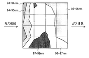
- FIG. 3 is a graph showing the film thickness uniformity of the alumina film formed on the substrate 42 having a length of 370 mm.times.width of 470 mm through the above steps
- FIG. 4 is a graph showing the film refractive index of the alumina film.
- the length of the side in the horizontal direction in FIG. 3 is 470 mm, and the length of the side in the vertical direction is 370 mm.
- These graphs represent film thickness uniformity and film refractive index when the substrate 42 is viewed from above.
- the left side is the gas supply side (upstream side)
- the right side is the gas exhaust side (downstream side).
- the upper side is the back side in FIG. 1, and the lower side is the near side.
- the thickness of the substrate surface is 93 to 98 nm, and 25 points on the substrate 42 (intersections of lines drawn in a lattice pattern and four points on the substrate 42 in the figure).
- the average film thickness was 96 nm.
- the film thickness distribution was about ⁇ 2.1%, and it was found that sufficient film thickness uniformity was obtained.
- the film refractive index of the alumina film (the refractive index at the interface between the alumina film and the surface of the substrate 42) is 1.61 to 1.64.
- the average film refractive index was about 1.626.
- the refractive index distribution is about ⁇ 0.5%, which indicates that a sufficient film refractive index is obtained, in other words, a sufficient film quality is obtained.
- the alumina film formed on the substrate 42 by the ALD apparatus 10 was sufficiently excellent in both film thickness uniformity and film refractive index (that is, film quality).
- membrane formed in this invention is not limited at all.
- the source gas should be appropriately determined according to the film to be formed.
- the source gas may be supplied to the substrate from the side wall side of the film formation container, or may be supplied to the substrate from the upper wall side through a shower head.
- the source gas may be exhausted from the side wall side of the film formation container, from the lower wall side, or from both the side wall side and the lower wall side.
- an oxidizing gas containing O is used as one of the reactive gases
- a nitriding gas containing N is used as one of the reactive gases.
- the source gas is a reaction gas mainly containing an element other than O among elements constituting the oxide film to be formed.
- the source gas is a reaction gas mainly composed of an element other than N among elements constituting the nitride film to be formed.
- the pressure, temperature, processing time, gas flow rate, etc. in the film formation container should be appropriately determined according to the type of film to be formed, the dimensions of the film formation container and the substrate, etc.
- the present invention is not limited to the above embodiment. Further, the material, shape and dimensions of the film forming container and the substrate stage are not limited at all.
- the antenna array includes a side wall of the film forming container to which the oxidizing gas is supplied in a horizontal direction from the gas supply unit, and a position on the side wall side of the film forming container to which the oxidizing gas is supplied at a position where the substrate is placed on the substrate stage. Provided in the space between the ends.
- the number of antenna elements is not limited, it is desirable to arrange the feeding positions between adjacent antenna elements so as to be side walls facing each other in consideration of the uniformity of the generated plasma. Further, there are no particular restrictions on the arrangement and dimensions of the antenna elements.
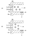
- each of the plurality of antenna elements may be arranged in a row in the horizontal direction, or may be arranged in a row in the vertical direction as shown in FIG.
- each of the antenna elements may be arranged in two or more rows in the horizontal direction, or in two or more columns in the vertical direction as shown in FIG. 6B. It may be arranged separately. At this time, it is desirable to arrange the rows or columns of adjacent antenna elements so that the positions of the antenna elements are staggered.
- an oxidizing gas is supplied horizontally into the film forming chamber, and plasma is generated by the antenna array to obtain oxygen radicals.
- plasma is not generated when the source gas is supplied into the deposition chamber. Therefore, the source gas may be supplied in the vertical direction from the upper wall side of the film formation container.
- a shower head is provided in the space between the upper wall of the film formation container and the substrate stage to diffuse the source gas evenly and prevent the source gas from being sprayed directly onto the substrate. desirable.
- the lifting mechanism 44 and the vacuum chamber 50 are not essential components.
- the configuration of the ALD apparatus according to the present invention in the absence of the elevating mechanism 44 and the vacuum chamber 50 is, for example, the arrangement of the antenna array 28 from above the substrate stage 32 in the conventional ALD apparatus 50 shown in FIGS.
- the structure is moved to the space between the side wall of the film formation container 12 and the substrate stage 32. In this case, the film forming container 12 becomes the film forming chamber 48.
- the present invention is basically as described above. As described above, the atomic layer growth apparatus and the thin film forming method of the present invention have been described in detail. However, the present invention is not limited to the above embodiment, and various improvements and modifications can be made without departing from the gist of the present invention. Of course it is good.
Landscapes
- Chemical & Material Sciences (AREA)
- Engineering & Computer Science (AREA)
- Physics & Mathematics (AREA)
- Plasma & Fusion (AREA)
- Chemical Kinetics & Catalysis (AREA)
- General Chemical & Material Sciences (AREA)
- Materials Engineering (AREA)
- Mechanical Engineering (AREA)
- Metallurgy (AREA)
- Organic Chemistry (AREA)
- Analytical Chemistry (AREA)
- Electromagnetism (AREA)
- Inorganic Chemistry (AREA)
- Chemical Vapour Deposition (AREA)
Abstract
Priority Applications (3)
| Application Number | Priority Date | Filing Date | Title |
|---|---|---|---|
| US12/863,565 US20110008550A1 (en) | 2008-01-25 | 2009-01-22 | Atomic layer growing apparatus and thin film forming method |
| KR1020107017247A KR101139220B1 (ko) | 2008-01-25 | 2009-01-22 | 원자층 성장 장치 및 박막 형성 방법 |
| JP2009523507A JP4540742B2 (ja) | 2008-01-25 | 2009-01-22 | 原子層成長装置および薄膜形成方法 |
Applications Claiming Priority (2)
| Application Number | Priority Date | Filing Date | Title |
|---|---|---|---|
| JP2008014647 | 2008-01-25 | ||
| JP2008-014647 | 2008-01-25 |
Publications (1)
| Publication Number | Publication Date |
|---|---|
| WO2009093459A1 true WO2009093459A1 (fr) | 2009-07-30 |
Family
ID=40900968
Family Applications (1)
| Application Number | Title | Priority Date | Filing Date |
|---|---|---|---|
| PCT/JP2009/000240 Ceased WO2009093459A1 (fr) | 2008-01-25 | 2009-01-22 | Appareil de développement de couche atomique et procédé de formation de film mince |
Country Status (5)
| Country | Link |
|---|---|
| US (1) | US20110008550A1 (fr) |
| JP (1) | JP4540742B2 (fr) |
| KR (1) | KR101139220B1 (fr) |
| TW (1) | TW200936804A (fr) |
| WO (1) | WO2009093459A1 (fr) |
Cited By (5)
| Publication number | Priority date | Publication date | Assignee | Title |
|---|---|---|---|---|
| JP2014220398A (ja) * | 2013-05-09 | 2014-11-20 | ソニー株式会社 | 原子層堆積装置及び原子層堆積方法 |
| US9306127B2 (en) | 2010-08-25 | 2016-04-05 | Nichia Corporation | Light emitting device that includes protective film having uniform thickness |
| JP2018152457A (ja) * | 2017-03-13 | 2018-09-27 | 株式会社デンソー | 半導体基板およびその製造方法 |
| KR20200051663A (ko) * | 2017-10-02 | 2020-05-13 | 도쿄엘렉트론가부시키가이샤 | 웨이퍼 제조 프로세스에서 초 국부적 및 플라즈마 균일성 제어 |
| CN112068501A (zh) * | 2019-06-11 | 2020-12-11 | 霍尼韦尔国际公司 | 具有现代架构和传统兼容性的过程控制设备 |
Families Citing this family (12)
| Publication number | Priority date | Publication date | Assignee | Title |
|---|---|---|---|---|
| JP4523661B1 (ja) * | 2009-03-10 | 2010-08-11 | 三井造船株式会社 | 原子層堆積装置及び薄膜形成方法 |
| JP5994986B2 (ja) * | 2012-09-20 | 2016-09-21 | シャープ株式会社 | 基地局装置、移動局装置および通信方法 |
| TWI469179B (zh) * | 2012-11-27 | 2015-01-11 | Ind Tech Res Inst | 電漿裝置 |
| WO2015145663A1 (fr) * | 2014-03-27 | 2015-10-01 | 株式会社日立国際電気 | Procédé de fabrication de dispositif à semi-conducteur et appareil de traitement de substrat |
| KR101570227B1 (ko) * | 2014-05-20 | 2015-11-18 | 주식회사 유진테크 | 기판 처리장치 및 기판 처리방법 |
| KR101656651B1 (ko) * | 2015-01-09 | 2016-09-22 | 주식회사 테스 | 박막증착장치 |
| KR101628786B1 (ko) * | 2015-09-09 | 2016-06-09 | 주식회사 유진테크 | 기판 처리장치 및 기판 처리방법 |
| US11424104B2 (en) | 2017-04-24 | 2022-08-23 | Applied Materials, Inc. | Plasma reactor with electrode filaments extending from ceiling |
| US11244808B2 (en) * | 2017-05-26 | 2022-02-08 | Applied Materials, Inc. | Monopole antenna array source for semiconductor process equipment |
| US11355321B2 (en) | 2017-06-22 | 2022-06-07 | Applied Materials, Inc. | Plasma reactor with electrode assembly for moving substrate |
| US11515122B2 (en) * | 2019-03-19 | 2022-11-29 | Tokyo Electron Limited | System and methods for VHF plasma processing |
| CN112609170B (zh) * | 2020-11-24 | 2022-12-09 | 鑫天虹(厦门)科技有限公司 | 原子层沉积设备与制程方法 |
Citations (5)
| Publication number | Priority date | Publication date | Assignee | Title |
|---|---|---|---|---|
| JPH04274317A (ja) * | 1991-03-01 | 1992-09-30 | Nippon Telegr & Teleph Corp <Ntt> | 薄膜形成方法およびその装置 |
| JP2003031565A (ja) * | 2001-07-18 | 2003-01-31 | Tokyo Electron Ltd | 半導体装置の製造方法、基板処理装置および基板処理システム |
| JP2004186534A (ja) * | 2002-12-05 | 2004-07-02 | Hitachi Kokusai Electric Inc | 基板処理装置 |
| WO2007114155A1 (fr) * | 2006-03-30 | 2007-10-11 | Mitsui Engineering & Shipbuilding Co., Ltd. | Procede et appareil pour la croissance par plasma de couches atomiques |
| JP2007273773A (ja) * | 2006-03-31 | 2007-10-18 | Mitsui Eng & Shipbuild Co Ltd | プラズマ処理装置およびプラズマ処理装置のクリーニング方法 |
Family Cites Families (1)
| Publication number | Priority date | Publication date | Assignee | Title |
|---|---|---|---|---|
| JPS58175824A (ja) * | 1983-03-28 | 1983-10-15 | Semiconductor Energy Lab Co Ltd | プラズマ気相反応用装置 |
-
2009
- 2009-01-22 WO PCT/JP2009/000240 patent/WO2009093459A1/fr not_active Ceased
- 2009-01-22 KR KR1020107017247A patent/KR101139220B1/ko not_active Expired - Fee Related
- 2009-01-22 US US12/863,565 patent/US20110008550A1/en not_active Abandoned
- 2009-01-22 JP JP2009523507A patent/JP4540742B2/ja not_active Expired - Fee Related
- 2009-01-23 TW TW098103113A patent/TW200936804A/zh unknown
Patent Citations (5)
| Publication number | Priority date | Publication date | Assignee | Title |
|---|---|---|---|---|
| JPH04274317A (ja) * | 1991-03-01 | 1992-09-30 | Nippon Telegr & Teleph Corp <Ntt> | 薄膜形成方法およびその装置 |
| JP2003031565A (ja) * | 2001-07-18 | 2003-01-31 | Tokyo Electron Ltd | 半導体装置の製造方法、基板処理装置および基板処理システム |
| JP2004186534A (ja) * | 2002-12-05 | 2004-07-02 | Hitachi Kokusai Electric Inc | 基板処理装置 |
| WO2007114155A1 (fr) * | 2006-03-30 | 2007-10-11 | Mitsui Engineering & Shipbuilding Co., Ltd. | Procede et appareil pour la croissance par plasma de couches atomiques |
| JP2007273773A (ja) * | 2006-03-31 | 2007-10-18 | Mitsui Eng & Shipbuild Co Ltd | プラズマ処理装置およびプラズマ処理装置のクリーニング方法 |
Cited By (11)
| Publication number | Priority date | Publication date | Assignee | Title |
|---|---|---|---|---|
| US9306127B2 (en) | 2010-08-25 | 2016-04-05 | Nichia Corporation | Light emitting device that includes protective film having uniform thickness |
| JP2014220398A (ja) * | 2013-05-09 | 2014-11-20 | ソニー株式会社 | 原子層堆積装置及び原子層堆積方法 |
| JP2018152457A (ja) * | 2017-03-13 | 2018-09-27 | 株式会社デンソー | 半導体基板およびその製造方法 |
| KR20200051663A (ko) * | 2017-10-02 | 2020-05-13 | 도쿄엘렉트론가부시키가이샤 | 웨이퍼 제조 프로세스에서 초 국부적 및 플라즈마 균일성 제어 |
| CN111183504A (zh) * | 2017-10-02 | 2020-05-19 | 东京毅力科创株式会社 | 制造过程中的超局部和等离子体均匀性控制 |
| JP2021503686A (ja) * | 2017-10-02 | 2021-02-12 | 東京エレクトロン株式会社 | 製造プロセスにおける超局所化及びプラズマ均一性制御 |
| US11551909B2 (en) | 2017-10-02 | 2023-01-10 | Tokyo Electron Limited | Ultra-localized and plasma uniformity control in a plasma processing system |
| JP7264576B2 (ja) | 2017-10-02 | 2023-04-25 | 東京エレクトロン株式会社 | 製造プロセスにおける超局所化及びプラズマ均一性制御 |
| CN111183504B (zh) * | 2017-10-02 | 2023-07-21 | 东京毅力科创株式会社 | 制造过程中的超局部和等离子体均匀性控制 |
| KR102766205B1 (ko) * | 2017-10-02 | 2025-02-10 | 도쿄엘렉트론가부시키가이샤 | 웨이퍼 제조 프로세스에서 초 국부적 및 플라즈마 균일성 제어 |
| CN112068501A (zh) * | 2019-06-11 | 2020-12-11 | 霍尼韦尔国际公司 | 具有现代架构和传统兼容性的过程控制设备 |
Also Published As
| Publication number | Publication date |
|---|---|
| JPWO2009093459A1 (ja) | 2011-05-26 |
| JP4540742B2 (ja) | 2010-09-08 |
| US20110008550A1 (en) | 2011-01-13 |
| TW200936804A (en) | 2009-09-01 |
| KR101139220B1 (ko) | 2012-04-23 |
| KR20100098461A (ko) | 2010-09-06 |
Similar Documents
| Publication | Publication Date | Title |
|---|---|---|
| JP4540742B2 (ja) | 原子層成長装置および薄膜形成方法 | |
| JP4426642B2 (ja) | 原子層成長装置および原子層成長方法 | |
| US9279184B2 (en) | Method of forming a pattern and substrate processing system | |
| US8440268B2 (en) | Method and apparatus for growing plasma atomic layer | |
| JP5735232B2 (ja) | プラズマ処理装置 | |
| JP4575998B2 (ja) | 薄膜形成装置および薄膜形成方法 | |
| JP2009191311A (ja) | 原子層成長装置 | |
| TWI621732B (zh) | 密封膜之形成方法及密封膜製造裝置 | |
| KR100724571B1 (ko) | 인시투 클리닝 기능을 갖는 플라즈마 처리장치 및 그사용방법 | |
| JP2009206312A (ja) | 成膜方法および成膜装置 | |
| WO2007040110A1 (fr) | Appareil et procédé de traitement au plasma | |
| JP5215685B2 (ja) | 原子層成長装置 | |
| JP2009194018A (ja) | 原子層成長装置および原子層成長方法 | |
| JP5052537B2 (ja) | プラズマ生成装置およびプラズマ生成方法 | |
| JP2024019774A (ja) | 成膜方法および成膜装置 | |
| JP5078656B2 (ja) | 原子層成長装置 | |
| JP4554712B2 (ja) | プラズマ処理装置 | |
| WO2011040537A1 (fr) | Procédé et appareil de traitement par plasma |
Legal Events
| Date | Code | Title | Description |
|---|---|---|---|
| WWE | Wipo information: entry into national phase |
Ref document number: 2009523507 Country of ref document: JP |
|
| 121 | Ep: the epo has been informed by wipo that ep was designated in this application |
Ref document number: 09703820 Country of ref document: EP Kind code of ref document: A1 |
|
| NENP | Non-entry into the national phase |
Ref country code: DE |
|
| ENP | Entry into the national phase |
Ref document number: 20107017247 Country of ref document: KR Kind code of ref document: A |
|
| WWE | Wipo information: entry into national phase |
Ref document number: 12863565 Country of ref document: US |
|
| 122 | Ep: pct application non-entry in european phase |
Ref document number: 09703820 Country of ref document: EP Kind code of ref document: A1 |