WO2009104573A1 - Substrat de réseaux détecteurs et dispositif de diagnostic médical nucléaire l'utilisant - Google Patents
Substrat de réseaux détecteurs et dispositif de diagnostic médical nucléaire l'utilisant Download PDFInfo
- Publication number
- WO2009104573A1 WO2009104573A1 PCT/JP2009/052626 JP2009052626W WO2009104573A1 WO 2009104573 A1 WO2009104573 A1 WO 2009104573A1 JP 2009052626 W JP2009052626 W JP 2009052626W WO 2009104573 A1 WO2009104573 A1 WO 2009104573A1
- Authority
- WO
- WIPO (PCT)
- Prior art keywords
- detection module
- detection
- detector array
- array substrate
- detectors
- Prior art date
- Legal status (The legal status is an assumption and is not a legal conclusion. Google has not performed a legal analysis and makes no representation as to the accuracy of the status listed.)
- Ceased
Links
Images




Classifications
-
- G—PHYSICS
- G01—MEASURING; TESTING
- G01T—MEASUREMENT OF NUCLEAR OR X-RADIATION
- G01T1/00—Measuring X-radiation, gamma radiation, corpuscular radiation, or cosmic radiation
- G01T1/16—Measuring radiation intensity
- G01T1/24—Measuring radiation intensity with semiconductor detectors
- G01T1/249—Measuring radiation intensity with semiconductor detectors specially adapted for use in SPECT or PET
-
- G—PHYSICS
- G01—MEASURING; TESTING
- G01T—MEASUREMENT OF NUCLEAR OR X-RADIATION
- G01T1/00—Measuring X-radiation, gamma radiation, corpuscular radiation, or cosmic radiation
- G01T1/16—Measuring radiation intensity
- G01T1/24—Measuring radiation intensity with semiconductor detectors
- G01T1/242—Stacked detectors, e.g. for depth information
-
- G—PHYSICS
- G01—MEASURING; TESTING
- G01T—MEASUREMENT OF NUCLEAR OR X-RADIATION
- G01T1/00—Measuring X-radiation, gamma radiation, corpuscular radiation, or cosmic radiation
- G01T1/16—Measuring radiation intensity
- G01T1/24—Measuring radiation intensity with semiconductor detectors
- G01T1/243—Modular detectors, e.g. arrays formed from self contained units
Definitions
- the present invention relates to a nuclear medicine diagnostic apparatus using radiation, and in particular, a detector array substrate suitable for Positron Emission computed Tomography (hereinafter referred to as "PET”) and the like, and nuclear medicine using the same. It relates to a diagnostic device.
- PET Positron Emission computed Tomography
- a nuclear medicine imaging apparatus is generally provided with an apparatus for administering a drug labeled with RI (radioisotope) to a subject such as a patient, detecting ⁇ -rays emitted from the RI, and acquiring the RI distribution in the subject.
- RI radioisotope
- Typical examples of nuclear medicine imaging devices include gamma cameras, single photon computed tomography (SPECT) devices, PET devices and the like.
- the ⁇ camera is a device that measures ⁇ rays emitted from the inside of the subject with a flat detector and images the flat distribution.
- a collimator is attached to the front of the detector to limit the incident direction of the ⁇ rays. It gives directionality.
- SPECT a flat panel detector similar to a ⁇ camera is placed around the subject to detect ⁇ rays emitted from the inside of the subject, and imaging processing is performed in the same manner as X-ray CT to obtain a body axis of RI distribution. It is an apparatus for imaging a tomogram or the like. Like the gamma camera, SPECT also has a collimator mounted on the front of the detector to limit the direction of gamma ray incidence.
- RI used for SPECT is a radionuclide that emits single ⁇ -ray, and for example, 99m Tc or 123 I is used, and these RI distributions can be imaged to obtain information on organ circulation and metabolism.
- the PET apparatus is an apparatus that detects a ⁇ -ray emitted from the inside of the subject by a ring detector disposed around the subject, performs imaging processing, and captures a body axial tomographic image of RI distribution and the like.
- a radioactive drug labeled with a positron ( ⁇ + ) emitting radionuclide is administered, and a pair of 511 keV annihilation ⁇ emits in approximately the opposite direction (180 ° ⁇ 0.6 °) when it emits ⁇ + to combine with an electron and annihilate The line is to be detected.
- the PET device can estimate the incident direction of two annihilation ⁇ -rays by selecting the ⁇ -rays detected at the same timing with a coincidence circuit, and therefore, unlike a ⁇ camera or SPECT, a mechanical collimator is used.
- Positron emitting nuclides used for PET imaging include 18 F, 15 O, 11 C and the like.
- tumor tissue has high sugar metabolism and is highly concentrated, it is possible to use fluorodeoxyglucose (2- [F-18] fluoro-2-deoxy-D-, which is an 18 F-labeled drug (a kind of sugar).
- glucose, 18 F-FDG is administered into a subject, the tracer 18 F also accumulates in tumor tissue.
- the tumor site can be identified quantitatively from the PET image at this time.
- a nuclear medicine imaging apparatus mainly uses a scintillator composed of a substance such as bismuth germanium oxide (BGO) or thallium-added sodium iodide (NaI (Tl)) as a detector for detecting ⁇ rays.
- BGO bismuth germanium oxide
- NaI (Tl) thallium-added sodium iodide
- the ⁇ ray incident on the detector is once converted to a weak light by a scintillator, and this weak light is converted to an electrical signal by a photomultiplier tube, a photodiode or the like. Therefore, there is a problem that the nuclear medicine imaging device is upsized.
- semiconductor detectors composed of semiconductor cells such as cadmium telluride (CdTe) and cadmium zinc telluride (CdZnTe) are currently attracting attention. These semiconductor detectors convert gamma rays directly into charge carriers (electrons and holes). Therefore, since ⁇ -rays can be detected in each semiconductor cell, it is expected that the size and weight of the device can be reduced as compared with the case where a scintillator and a photomultiplier are used. Also, the number of charge carriers generated is much larger than that obtained by the scintillator detector, which means that good energy resolution can be obtained.
- the energy resolution refers to the ability to detect the value of the energy of gamma rays with high accuracy. For example, 511 keV gamma rays can be correctly detected as 511 keV energy.
- a detection module having a structure in which a plurality of semiconductor radiation detection elements are laminated via a metal plate, the lamination surface is perpendicular to the wiring substrate are arranged in
- the feature of the semiconductor detector is good energy resolution, and good energy resolution leads to the advantages of high definition and high quantitativity in image diagnosis. And this advantage becomes more remarkable with the improvement of spatial resolution and detection sensitivity.
- the spatial resolution refers to the ability to accurately detect the emission position of gamma rays.
- semiconductor devices represented by CdTe are generally sensitive to mechanical shocks and defects, and for the purpose of protecting them, the surface is protected and supported by a metal plate as shown in FIG. 5 of Patent Document 1 After fixing the metal plate to the semiconductor element, it is attached to the substrate. Further, in the case where a huge number of detectors are mounted on a wiring board as in a PET device, it is desirable that the automatic mounting device can handle the same from the viewpoint of cost reduction. However, in this case, in consideration of the mounting position error of the device, it is necessary to provide a fixed gap so that each detection module does not abut.
- An object of the present invention is to provide a detector array substrate capable of improving detection sensitivity and spatial resolution, and a nuclear medicine diagnostic apparatus using the same, in view of the above-mentioned situation.
- the detector array substrate according to the first aspect of the present invention has a Z direction in the same direction as the body axis of the subject, a Y direction in substantially the same direction as the radiation incident direction from the radioactive substance in the subject, the Z direction and the Y direction.
- a detection module is provided, and the detection module having the plurality of detectors is disposed in the X direction with respect to the XZ plane for detecting the radiation, and both planes of the wiring substrate in the Z direction or
- the detector is laminated by placing the detection module in a flat structure to a plane, it is provided with a plurality of the detection module to the Y direction.
- a nuclear medicine diagnosis apparatus comprises a detector arrangement structure in which a plurality of the detector arrangement substrates according to the first invention are arranged in the Z direction.
- a detector array substrate capable of improving detection sensitivity and spatial resolution and a nuclear medicine diagnostic apparatus using the same can be realized.
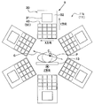
- FIG. 2 is a conceptual sectional view taken along line AA of FIG. 1 showing a main part structure of a detection unit for detecting an annihilation ⁇ -ray pair inside a gantry of a PET apparatus during an inspection of a subject (indicated by a two-dot chain line in FIG. 1). .
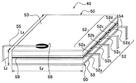
- FIG. 4 is an enlarged perspective view of a detection module mounted on the wiring substrate of the detector array substrate shown in FIG. 3; It is a perspective view which shows the detection element which comprises a detection module. It is a perspective view which shows an assembly of a detection module. It is a perspective view showing a detector arrangement substrate of modification.
- a PET apparatus 1 of a nuclear medicine diagnostic apparatus has a bed 13 on which a subject P such as a patient who receives a drug labeled with a positron emitting nuclide is placed.
- the object P on 13 is moved in the direction of the arrow .alpha.
- FIG. 1 is a perspective view showing the entire configuration of the PET apparatus 1.
- the input / output operation device 15 having the display device 14 etc. is placed in the examination room (at least the gantry 11, the bed 13 etc. is disposed in order to avoid radiation exposure of the inspection technician who operates the input / output operation device 15). Not shown) is arranged outside.
- FIG. 2 shows a main part structure of a detection unit 11 k for detecting an annihilation ⁇ -ray pair inside the gantry 11 of the PET apparatus 1 under test when the object P (indicated by a two-dot chain line in FIG. It is a -A line cross section conceptual diagram.
- the detection unit 11 k in the gantry 11 has a plurality of CdTe (cadmium telluride) semiconductor detection elements 50 that detect ⁇ rays from the accumulation unit C of the positron-emitting nuclide in the subject P.
- CdTe cadmium telluride
- a detector array substrate 30 having a detection module 40 and a signal processing unit 31 for processing a detection signal by the ⁇ -ray of the detection module 40 is paired in such a manner as to face each other with the subject P on the bed 13 as the center. It has a total of six.
- the detector array substrate 30 can also be configured without facing each other.
- the X direction, the Y direction, and the Z direction shown in FIG. 1 and FIG. 2 etc. are determined as follows.
- the Z direction (the direction perpendicular to the sheet of FIG. 2) shown in FIGS. 1 and 2 refers to the same direction as the body axis direction of the subject P.
- the detector array substrate 30 having the detection module 40 is annularly disposed in the Z direction (the direction perpendicular to the sheet of FIG. 2), that is, around the body axial direction of the subject P, and the X direction in FIG.
- the circumferential direction around the subject P in the PET apparatus 1, ie, the tangential direction refers to the Y direction in FIG.
- the radial direction around the subject P ie, the positron-emitting nuclide in the subject P. It refers to the direction in which the annihilation gamma ray pair emitted from the accumulation portion C is mainly incident.
- the detector array substrate 30 is illustrated in plan view, so the detector array substrate 30 appears to be overlapped in the vertical direction on the paper surface of FIG.
- a plurality of detectors P are arranged in the body axis direction of the subject P, that is, in the Z direction (see FIG. 3 in a perspective view of the detector array substrate 30 in FIG. 2 viewed from the B direction) It has a three-dimensional structure.
- a voltage is applied to the CdTe semiconductor single crystal constituting the detection module 40, an electric signal corresponding to the amount and energy of radiation can be detected, so that the CdTe semiconductor single crystal of the detection module 40 It absorbs efficiently and converts it directly into an electrical signal, which has high detection sensitivity for ⁇ -rays and good energy resolution.
- the signal processing unit 31 of the detection module 40 mounted on the detector array substrate 30 shown in FIG. 2 is composed of a signal processing circuit etc., and performs waveform shaping and amplification of the electric signal output from the detection module 40 upon incidence of ⁇ rays.
- Voltage-signal wave height (equivalent to the energy of ⁇ -ray), amplifier address-detector XY address conversion, acquisition of data time information, and characteristics such as thickness of individual CdTe semiconductor detection elements
- Signal processing such as real-time wave height calibration for correcting
- FIG. 3 is an enlarged perspective view of one detector array substrate 30 of FIG. 2 as viewed from the direction B, and the signal processing unit 31 is omitted.
- the signal processing unit 31 when the signal processing unit 31 is illustrated, the signal processing unit 31 is illustrated on the right side of the drawing of FIG. 3, and ⁇ rays from the accumulation unit C of positron-emitting nuclides are shown in FIG. The light is incident on the detector array substrate 30 from the left to the right.
- the detection module 40 is inclined from the surface side of the paper surface of FIG. 3 corresponding to the circumferential direction (see FIG. 2) of the object P around the PET apparatus 1.
- Four are arranged on the back surface side, and four are arranged mainly in the Y direction (left and right direction in the sheet of FIG. 3) in the direction in which ⁇ rays are incident.
- a total of two detection modules 40 are disposed on both sides of the wiring substrate 32 in the vertical direction in the drawing of FIG. 3 and the detection modules 40 are mounted in a flat structure on the wiring substrate 32 using the conductive adhesive 60. As shown in FIG.
- FIG. 3 illustrates the case where the two detector array substrates 30 are arranged in the Z direction.
- FIG. 4 is an enlarged perspective view of the detection module 40 mounted on the wiring board 32 of the detector array substrate 30 shown in FIG. 3, and FIG. 5 is a perspective view showing the detection element 50 constituting the detection module 40. is there.
- the detection module 40 in the detection module 40, two detection elements 50 shown in FIG. 5 have their anodes facing each other, and the signal electrodes 52 (52a, 52b, 52c, 52d) on one side face each other.
- the conductive adhesive 59 is used for bonding.
- the upper and lower end portions (upper and lower surface sides of the detection module 40 shown in FIG. 4) of the detection module 40 are cathodes, and the bias electrodes 53 are formed on the upper and lower surfaces.
- the detection element 50 constituting the detection module 40 is pattern-coated in four sections using conductive In (indium) on one surface of a CdTe semiconductor crystal 51 made of CdTe (cadmium telluride).
- the signal electrode 52 (52a, 52b, 52c, 52d) is formed, and the bias electrode 53 coated with conductive Pt (platinum) that is resistant to oxidation is formed on the entire surface of the other surface of the semiconductor crystal 51.
- each of the four divided signal electrodes 52 of one surface of the semiconductor crystal 51 of the detection element 50 is an electrical signal obtained by converting ⁇ rays in the CdTe semiconductor crystal 51
- the potential of the signal electrode 52 on the anode side is approximately 0V.
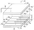
- FIG. 6 is a perspective view showing the assembly of the detection module 40.
- the pair of detection elements 50 are opposed to each other such that the signal electrodes 52 (52a, 52b, 52c, 52d) on the anode side face each other.
- the conductor 54 54a, 54b, 54c, 54d
- the conductor 54 54a, 54b, 54c, 54d of copper ribbon shape or wire about several 10 ⁇ m thick is sandwiched between the respective pair of signal electrodes 52 (52a, 52b, 52c, 52d) It bonds together using the adhesive 59.
- the dimension between the detection elements 50 to be bonded is narrowed, and the spatial resolution in the Z direction shown in FIG. 2 is improved.
- a conductor 55 for applying a reverse bias voltage is connected to the surface of the bias electrode 53 of the upper detection element 50 using a conductive adhesive 56, and the detection shown in FIG. A module 40 is configured.
- the detection module 40 has a large bonding area because the large surfaces of the signal electrodes 52 of the two detection elements 50 are bonded to each other, and the strength is enhanced as the flat detection module 40.
- a reverse bias voltage is supplied to the bias electrode 53 of the outer (upper in FIG. 4) detection element 50 using the conductor 55
- a reverse bias voltage is supplied to the bias electrode 53 of the inner (lower in FIG. 4) detection element 50 using a wire (not shown) formed on the wiring substrate 32 (see FIG. 3).
- the detection signal by the ⁇ ray incident on the detection element 50 through the copper ribbon or wire conductors 54a, 54b, 54c, 54d of the respective signal electrodes 52a, 52b, 52c, 52d of the detection module 40 It is read out.
- the detection module 40 (see FIG. 4) of this configuration has the one side 32 a and the other side 32 a of the wiring board 32 around the object P under inspection of the PET device 1.
- Four pieces are arranged in the circumferential direction (see FIG. 2) in the X direction (from the surface side in the sheet of FIG. 3 to the oblique back side, see FIG. 2), and also in the Y direction (FIG. 3) 4 in the left-right direction in the sheet of the drawing, and in the Z direction of the body axis direction of the subject P (in the vertical direction in the sheet of FIG. 3), using the conductive adhesive 60 It is mounted on the wiring board 32.
- FIG. 2 shows that the conductive adhesive 60
- the detection module 40 is placed on the wiring substrate 32 so that the flat surface 32 a of the wiring substrate 32 and the electrode surface of the bias electrode 53 of the detection module 40 are parallel (corresponding to the XY plane, see FIG. 2). It is mounted. That is, the detection module 40 is configured to have a flat structure with respect to the wiring board 32, and the detection module 40 which is weak in strength is supported by the wiring board 32 on a wide surface with the bias electrode 53 The strength improvement of 40 is achieved.
- the wiring board 32 on which the detection module 40 is mounted has a multilayer (not shown) for signal readout signal electrode 52, a wiring 32h for bias electrode 53 for bias voltage application, etc. It is a wiring board, and each wiring is formed independently by embedding the wiring in the wiring board 32 or the like.
- a signal processing unit 31 (not shown in FIG. 3, see FIG. 2) is provided on the back side in the Y direction of the direction in which the ⁇ ray mainly enters in the wiring substrate 32.
- the respective conductors 54 for the signal electrode 52 connected to the signal electrodes 52 (52a, 52b, 52c, 52d) (see FIG. 4) are mainly in the Y direction (the left and right of the sheet of FIG. Extends in the direction) and is connected to the signal current wiring (not shown) formed on the wiring substrate 32 by a conductive adhesive.
- the bias electrode surface 53 in direct contact with the wiring substrate 32 of the detection module 40 is directly bonded to the wiring substrate 32 using a conductive adhesive without using a conductor, and is formed on the wiring substrate 32. Are connected to the wiring (not shown).
- the conductor 55 for the bias electrode 53 on the top of each detection module 40 mainly extends in the Y direction (the left and right direction in the drawing of FIG. 3) in which the ⁇ ray is incident, and the conductive adhesive It is connected to the wiring 32 h for bias voltage formed in As can be seen from FIG.
- all the conductors for connection of the conductor 54 for the signal electrode 52 (52 a, 52 b, 52 c, 52 d) of each detection module 40 and the conductor 55 for the bias electrode 53 are mainly ⁇ rays incident. It is connected to the wiring board 1 in a form along the Y direction of the direction of
- a bias voltage application wiring applies a reverse bias voltage of the same potential, only one bias voltage application wiring is sufficient.
- the detection module 40 is mounted mainly in the Y direction (see FIGS. 3 and 2) in the direction in which ⁇ rays are incident, the detection module 40 is placed so that CdTe semiconductors of the same type, ie, the same potential face each other. It is desirable to mount on the wiring board 1 while facing each other alternately.
- the conductor 54 for the signal electrode has a potential of about 0 V and the conductor 55 for the bias electrode has a potential of several hundreds V, the possibility of dielectric breakdown due to a large potential difference is eliminated by facing each other. This is because the spacing between the detection modules 40 in the Y direction in which light is incident can be easily reduced, the density of the CdTe semiconductor can be improved, and as a result, the detection sensitivity of .gamma.
- the reverse bias voltage is supplied to the bias electrode 53 of the detection module 40, the positions of the anode and the cathode of the detection element 50 may be exchanged.
- the case where the two anodes are made to face each other and two detection elements 50 (see FIG. 4) are stacked on the wiring substrate 32 is illustrated.
- the anode or the cathode of the detection elements 50 is made to face each other It is possible to stack an arbitrary number of detection elements 50 as appropriate.
- FIG. 7 is a perspective view showing a detector array substrate 30 'of a modified embodiment.
- the detector array substrate 30 'of the modified embodiment shown in FIG. 7 has a structure in which detection sensitivity and spatial resolution are improved specifically in the Z direction (see FIGS. 1 and 2) of the body axis direction of the subject P.
- the detector array substrate 30 'of the modified embodiment is a detection module 40' in which detection elements 50a 'and 50b' having different dimensions in the Y direction (left and right direction of the paper surface of FIG. 7) Is used.
- the signal electrode 52' (52a ', 52b', 52c ', 52d') from the signal electrode 52 '(52a', 52b ', 52c', 52d ') where the dimension of the detection element 50a' with the longer dimension protrudes from the shorter detection element 50b '
- a conductor 54 'for 52' is drawn out to read out a signal.
- the configuration other than this is the same as that of the embodiment, so the same components as the embodiment are indicated by adding '(dash) to the reference numerals of the embodiment, and the detailed description will be omitted.
- the conductor 54 ' is not present between the detection elements 50a' and 50b 'in bonding the detection elements 50a' and 50b ', so that the thickness of the conductor 54' can be eliminated in the detection module 40 '.
- the density of the CdTe semiconductor in the Z direction (see FIGS. 1 and 2) in the body axis direction of the subject P is improved.
- the conductor 54 ' is drawn out from the signal electrode 52' exposed to the outside of the portion where the detection module 50 'has a longer dimension, and the dimension of the detection device 50a' having a longer dimension is shorter. Wiring is easy.
- a detection element 50 patterned using signal electrodes 52 (52a, 52b, 52c, 52d) of a plurality of read electrodes is used.
- the detection element 50 is formed by bonding and overlapping the signal electrodes 52 (52a, 52b, 52c, 52d) of the read electrodes to face each other as a detection module 40, and one detection module It is structured to be able to read out ⁇ -ray detection signals of a plurality of channels from 40 to 40.
- the detection module 40 wiring is performed such that the flat surface 32 a on which the wiring substrate 32 extends and the respective electrode surfaces 52 (52 a, 52 b, 52 c, 52 d) and 53 of the detection element 50 are parallel. It is mounted on the substrate 32.
- the plurality of detection modules 40 are installed in the Y direction orthogonal to the plane (XZ plane) on which the ⁇ ray mainly enters. That is, the detection module 40 has a structure having a plurality of detectors in the X direction, and the detection elements 50 are stacked in the Z direction (see FIGS. 1 and 2).
- connection of the signal electrodes 52 (52a, 52b, 52c, 52d) and the bias electrode 53 from each detection module 40 is wired at a position on the Y direction side with respect to each Connect to the substrate 32.
- a wire or ribbon conductor is used as a member for connecting the signal electrode 52 and the bias electrode 53 of the detection module 40 and the wiring substrate 32.
- a plurality of detector array substrates 30 configured as described above are arranged in the Z direction, and the detector array substrate 30 is annularly disposed around the subject P such that the Z direction is the body axis direction. Configured.
- the detection element 50 (FIG. 2) patterned in the signal electrode 52 (52a, 52b, 52c, 52d) in the X direction of the circumferential direction (see FIG. 2)
- the dead space occupation ratio between the detection elements 50 in the X direction can be suppressed, and dense arrangement becomes possible, and detection sensitivity can be improved.
- spatial resolution is also improved.
- the detection pitch in the X direction can be freely adjusted by adjusting the width dimension s of the signal electrode 52 shown in FIG. 5 which is the pattern width. That is, the spatial resolution in the X direction in the circumferential direction (see FIG. 2) of the PET apparatus 1 is improved.
- signals are read out from the respective detection modules 40 mainly in the Y direction in which ⁇ rays are incident, and ⁇ rays are mainly incident on the detector array substrate 30. Since CdTe semiconductors of the same potential face each other in the Y direction (see FIGS. 3 and 2) of the direction, unnecessary crosstalk (deterioration of signal accuracy) of the detection signal can be suppressed in the Y direction. . This leads to maintaining the good energy resolution which is a feature of the semiconductor detector, and as a result, a high definition and high quantitative image can be obtained.
- the density of the CdTe semiconductor of the detector array substrate 30 having the detection module 40 is improved, and ⁇ rays can be efficiently detected in the Y direction in which ⁇ rays are mainly incident. . Therefore, it is possible to simultaneously improve the spatial resolution as well as the detection sensitivity of the ⁇ -rays. Therefore, in the PET apparatus 1, it is possible to provide a high definition and high quantitative image.
- the detector module 40 is disposed on both flat surfaces 32 a of the wiring substrate 32.
- the detector module 40 may be disposed on one flat surface 32 a of the wiring substrate 32.
- the case where two detector array substrates 30 are arranged in the Z direction of the body axis direction of the subject P has been illustrated, it is possible to arrange an arbitrary number of detector array substrates 30.
- each dimension and the number of members illustrated by this embodiment are an example, and are not limited to these figures.
Landscapes
- Physics & Mathematics (AREA)
- Health & Medical Sciences (AREA)
- Life Sciences & Earth Sciences (AREA)
- General Physics & Mathematics (AREA)
- High Energy & Nuclear Physics (AREA)
- Molecular Biology (AREA)
- Spectroscopy & Molecular Physics (AREA)
- Measurement Of Radiation (AREA)
- Nuclear Medicine (AREA)
Abstract
L'invention concerne un substrat de réseaux détecteurs et un dispositif de diagnostic médical nucléaire l'utilisant. Le substrat de réseaux de détecteur comprend un module de détection plat formé par empilement de plusieurs éléments de détection qui, afin de former plusieurs détecteurs pour détecter un rayonnement, sont raccordés aux détecteurs, respectivement, et comportent des électrodes de signaux pour lire des signaux des détecteurs respectifs et des électrodes de polarisation pour appliquer une tension de polarisation aux détecteurs respectifs. Dans un plan XZ dans lequel le rayonnement est détecté, plusieurs modules de détection comportant des détecteurs sont disposés dans une direction X, un module de détection est disposé sur chaque surface ou sur une surface d'une carte de circuit imprimé dans une structure plate dans une direction Z pour empiler ainsi des détecteurs, et plusieurs modules de détection sont prévus dans une direction Y.
Priority Applications (1)
| Application Number | Priority Date | Filing Date | Title |
|---|---|---|---|
| US12/857,950 US20100308230A1 (en) | 2008-02-22 | 2010-08-17 | Detector array substrate and nuclear medicine diagnosis device using same |
Applications Claiming Priority (2)
| Application Number | Priority Date | Filing Date | Title |
|---|---|---|---|
| JP2008040853A JP2009198343A (ja) | 2008-02-22 | 2008-02-22 | 検出器配列基板およびこれを用いた核医学診断装置 |
| JP2008-040853 | 2008-02-22 |
Related Child Applications (1)
| Application Number | Title | Priority Date | Filing Date |
|---|---|---|---|
| US12/857,950 Continuation US20100308230A1 (en) | 2008-02-22 | 2010-08-17 | Detector array substrate and nuclear medicine diagnosis device using same |
Publications (1)
| Publication Number | Publication Date |
|---|---|
| WO2009104573A1 true WO2009104573A1 (fr) | 2009-08-27 |
Family
ID=40985453
Family Applications (1)
| Application Number | Title | Priority Date | Filing Date |
|---|---|---|---|
| PCT/JP2009/052626 Ceased WO2009104573A1 (fr) | 2008-02-22 | 2009-02-17 | Substrat de réseaux détecteurs et dispositif de diagnostic médical nucléaire l'utilisant |
Country Status (3)
| Country | Link |
|---|---|
| US (1) | US20100308230A1 (fr) |
| JP (1) | JP2009198343A (fr) |
| WO (1) | WO2009104573A1 (fr) |
Cited By (1)
| Publication number | Priority date | Publication date | Assignee | Title |
|---|---|---|---|---|
| CN109223015A (zh) * | 2017-07-10 | 2019-01-18 | 西门子医疗有限公司 | 具有中间单元和评估层级的x射线检测器 |
Families Citing this family (9)
| Publication number | Priority date | Publication date | Assignee | Title |
|---|---|---|---|---|
| WO2010058309A2 (fr) * | 2008-11-18 | 2010-05-27 | Koninklijke Philips Electronics N.V. | Détecteur spectral de formation d'images |
| JP5711476B2 (ja) | 2010-07-29 | 2015-04-30 | 日立アロカメディカル株式会社 | 放射線検出器カード |
| JP5569842B2 (ja) | 2010-08-04 | 2014-08-13 | 日立アロカメディカル株式会社 | 放射線検出器及び放射線検出装置 |
| US20120193545A1 (en) * | 2011-01-31 | 2012-08-02 | General Electric Company | Detector systems with anode incidence face and methods of fabricating the same |
| FR2972268B1 (fr) * | 2011-03-01 | 2013-03-29 | Sagem Defense Securite | Detecteur de sursauts gamma compact a haute resolution |
| JP2014194375A (ja) * | 2013-03-29 | 2014-10-09 | Hitachi Aloka Medical Ltd | 放射線測定装置 |
| DE102014222690B4 (de) * | 2014-11-06 | 2024-10-02 | Siemens Healthineers Ag | Detektormodul für einen Röntgendetektor |
| CZ29250U1 (cs) * | 2016-01-29 | 2016-03-08 | Advacam S.R.O. | Vrstvený pixelový detektor ionizujícího záření |
| JP6692237B2 (ja) * | 2016-07-19 | 2020-05-13 | 株式会社日立製作所 | 放射線検出器 |
Citations (1)
| Publication number | Priority date | Publication date | Assignee | Title |
|---|---|---|---|---|
| JP2007078369A (ja) * | 2005-09-09 | 2007-03-29 | Hitachi Ltd | 放射線検出モジュール、プリント基板および陽電子放出型断層撮影装置 |
Family Cites Families (2)
| Publication number | Priority date | Publication date | Assignee | Title |
|---|---|---|---|---|
| US4700076A (en) * | 1983-09-02 | 1987-10-13 | Digital Imaging Company Of America, Inc. | Solid-state X-ray receptor and method of making same |
| JP2005106692A (ja) * | 2003-09-30 | 2005-04-21 | Hitachi Ltd | 半導体放射線検出器及び放射線撮像装置 |
-
2008
- 2008-02-22 JP JP2008040853A patent/JP2009198343A/ja active Pending
-
2009
- 2009-02-17 WO PCT/JP2009/052626 patent/WO2009104573A1/fr not_active Ceased
-
2010
- 2010-08-17 US US12/857,950 patent/US20100308230A1/en not_active Abandoned
Patent Citations (1)
| Publication number | Priority date | Publication date | Assignee | Title |
|---|---|---|---|---|
| JP2007078369A (ja) * | 2005-09-09 | 2007-03-29 | Hitachi Ltd | 放射線検出モジュール、プリント基板および陽電子放出型断層撮影装置 |
Cited By (1)
| Publication number | Priority date | Publication date | Assignee | Title |
|---|---|---|---|---|
| CN109223015A (zh) * | 2017-07-10 | 2019-01-18 | 西门子医疗有限公司 | 具有中间单元和评估层级的x射线检测器 |
Also Published As
| Publication number | Publication date |
|---|---|
| JP2009198343A (ja) | 2009-09-03 |
| US20100308230A1 (en) | 2010-12-09 |
Similar Documents
| Publication | Publication Date | Title |
|---|---|---|
| WO2009104573A1 (fr) | Substrat de réseaux détecteurs et dispositif de diagnostic médical nucléaire l'utilisant | |
| US7297955B2 (en) | Semiconductor radiation detector, positron emission tomography apparatus, semiconductor radiation detection apparatus, detector unit and nuclear medicine diagnostic apparatus | |
| JP3858044B1 (ja) | 放射線検出モジュール、プリント基板および陽電子放出型断層撮影装置 | |
| JP4594624B2 (ja) | 放射線検出装置および核医学診断装置 | |
| KR101104173B1 (ko) | 방사선 검출기 및 방사선 검사장치 | |
| US20110253901A1 (en) | Device for detecting highly energetic photons | |
| RU2605523C2 (ru) | Чувствительное к излучению детекторное устройство с отклоняющими заряд зазорами между сегментами | |
| JP3828896B2 (ja) | 陽電子放出型断層撮影装置 | |
| CN101326449A (zh) | 放射线检测单元以及放射线检查装置 | |
| JPH11337646A (ja) | 放射線半導体検出器、放射線半導体検出器アレイおよびコリメータ設置装置 | |
| JP4178402B2 (ja) | 放射線検出器 | |
| JP3976259B2 (ja) | ポジトロンエミッショントモグラフィ装置 | |
| JP2007051896A (ja) | 半導体放射線検出器、放射線検出モジュールおよび核医学診断装置 | |
| JP4582022B2 (ja) | 放射線検出器,放射線検出素子及び放射線撮像装置 | |
| JP4464998B2 (ja) | 半導体検出器モジュール、および該半導体検出器モジュールを用いた放射線検出装置または核医学診断装置 | |
| JP3815468B2 (ja) | 放射線検出器,放射線検出素子及び放射線撮像装置 | |
| JP2000056021A (ja) | 放射線検出器および核医学診断装置 | |
| JP4834427B2 (ja) | 放射線検出モジュール、プリント基板および核医学診断装置 |
Legal Events
| Date | Code | Title | Description |
|---|---|---|---|
| 121 | Ep: the epo has been informed by wipo that ep was designated in this application |
Ref document number: 09711808 Country of ref document: EP Kind code of ref document: A1 |
|
| NENP | Non-entry into the national phase |
Ref country code: DE |
|
| 122 | Ep: pct application non-entry in european phase |
Ref document number: 09711808 Country of ref document: EP Kind code of ref document: A1 |