WO2009107532A1 - Résonateur composite, filtre passe-bande, diplexeur et module de communication sans fil et dispositif de communication sans fil utilisant le résonateur composite, le filtre passe-bande et le diplexeur - Google Patents
Résonateur composite, filtre passe-bande, diplexeur et module de communication sans fil et dispositif de communication sans fil utilisant le résonateur composite, le filtre passe-bande et le diplexeur Download PDFInfo
- Publication number
- WO2009107532A1 WO2009107532A1 PCT/JP2009/052811 JP2009052811W WO2009107532A1 WO 2009107532 A1 WO2009107532 A1 WO 2009107532A1 JP 2009052811 W JP2009052811 W JP 2009052811W WO 2009107532 A1 WO2009107532 A1 WO 2009107532A1
- Authority
- WO
- WIPO (PCT)
- Prior art keywords
- electrode
- input
- composite
- output
- composite resonance
- Prior art date
- Legal status (The legal status is an assumption and is not a legal conclusion. Google has not performed a legal analysis and makes no representation as to the accuracy of the status listed.)
- Ceased
Links
Images










Classifications
-
- H—ELECTRICITY
- H01—ELECTRIC ELEMENTS
- H01P—WAVEGUIDES; RESONATORS, LINES, OR OTHER DEVICES OF THE WAVEGUIDE TYPE
- H01P1/00—Auxiliary devices
- H01P1/20—Frequency-selective devices, e.g. filters
- H01P1/201—Filters for transverse electromagnetic waves
- H01P1/203—Strip line filters
- H01P1/2039—Galvanic coupling between Input/Output
-
- H—ELECTRICITY
- H01—ELECTRIC ELEMENTS
- H01P—WAVEGUIDES; RESONATORS, LINES, OR OTHER DEVICES OF THE WAVEGUIDE TYPE
- H01P1/00—Auxiliary devices
- H01P1/20—Frequency-selective devices, e.g. filters
- H01P1/201—Filters for transverse electromagnetic waves
- H01P1/203—Strip line filters
- H01P1/20327—Electromagnetic interstage coupling
- H01P1/20336—Comb or interdigital filters
- H01P1/20345—Multilayer filters
-
- H—ELECTRICITY
- H01—ELECTRIC ELEMENTS
- H01P—WAVEGUIDES; RESONATORS, LINES, OR OTHER DEVICES OF THE WAVEGUIDE TYPE
- H01P1/00—Auxiliary devices
- H01P1/20—Frequency-selective devices, e.g. filters
- H01P1/213—Frequency-selective devices, e.g. filters combining or separating two or more different frequencies
- H01P1/2135—Frequency-selective devices, e.g. filters combining or separating two or more different frequencies using strip line filters
Definitions
- the present invention relates to a resonator used in a filter circuit, an oscillation circuit, and the like, and more particularly to a composite resonator having a plurality of resonance frequencies that can easily realize a broadband bandpass filter. .
- the present invention also relates to a bandpass filter, a radio communication module and a radio communication device using the same, and more particularly to a bandpass filter having a very wide pass band, and a radio communication module and a radio communication device using the same. Is.
- the present invention relates to a diplexer, a radio communication module and a radio communication device using the diplexer, and in particular, a diplexer capable of demultiplexing and multiplexing two signals having a very wide frequency band, and the same
- the present invention relates to a used wireless communication module and a wireless communication device.
- UWB has attracted attention as a new communication means.
- UWB realizes large-capacity data transfer using a wide frequency band at a short distance of about 10 m.
- a frequency band of 3.1 to 10.6 GHz is realized. It is planned to be used.
- the feature of UWB is that it uses a very wide frequency band.
- research on a bandpass filter having a very wide passband that can be used for UWB has been actively conducted. For example, a bandpass filter that applies the principle of a directional coupler can reduce the passband width.
- the plan divided into two is drawn up. Therefore, the Low Band filter that passes the Low Band and the High Band filter that passes the High Band are required to have both a pass bandwidth of about 40% to 50% and an attenuation at 5.3 GHz, respectively. Therefore, “Ultra-wideband bandpass filter using a microstrip-CPW broadside coupling structure” having characteristics such that the passband width exceeds 100% in the specific band. -2-114 p.
- the band-pass filter proposed in 147 cannot be used because its pass bandwidth is too wide.
- the pass band width of a conventional band pass filter using a quarter wavelength resonator is too narrow, and even if the pass band width of the band pass filter described in Japanese Patent Laid-Open No. 2004-180032 is intended to widen the band.
- the specific band was less than 10%. Therefore, it could not be used as a UWB band-pass filter that requires a wide pass bandwidth corresponding to 40% to 50% in the specific band.
- the antenna side has two terminals because the circuit that processes the Low Band signal and the circuit that processes the High Band signal are different.
- the necessity of a diplexer for connecting the Low Band side terminal and the High Band side terminal to the antenna has increased. In such a diplexer, it is necessary that sufficient isolation is ensured between the terminal on the Low Band side and the terminal on the High Band side.
- the present invention has been devised in view of such problems in the prior art, and an object of the present invention is to easily construct a bandpass filter having a very wide and desired passband. Another object of the present invention is to provide a composite resonator capable of arbitrarily setting two resonance frequencies to some extent. Another object of the present invention is to provide a bandpass filter having a very wide and desired passband, and a wireless communication module and a wireless communication device using the same. Still another object of the present invention is to be able to demultiplex and multiplex two signals having a very wide frequency band, and to provide a diplexer with excellent isolation characteristics, and a radio communication module and radio using the diplexer It is to provide communication equipment.
- the composite resonator of the present invention includes a laminate, a ground electrode, and a composite resonant electrode.
- the laminate is formed by laminating a plurality of dielectric layers.
- the ground electrode is disposed on the lower surface of the laminate.
- the composite resonance electrode is disposed on the upper surface or inside the stacked body.
- the composite resonance electrode includes a base and a plurality of strip-shaped protrusions. One end of the base is grounded.
- the plurality of protrusions are arranged side by side with one end connected to the other end of the base.
- the one end of the base is one end of the composite resonance electrode, and the other end of the protrusion is the other end of the composite resonance electrode.
- the band-pass filter of the present invention includes a laminate, a ground electrode, a composite resonance electrode, a strip-shaped input coupling electrode, and a strip-shaped output coupling electrode.
- the laminate is formed by laminating a plurality of dielectric layers.
- the ground electrode is disposed on the lower surface of the laminate.
- the composite resonance electrode is disposed between the first layers of the multilayer body.
- the composite resonance electrode includes a base and a plurality of strip-shaped protrusions.
- the base is grounded.
- the plurality of protrusions are arranged side by side with one end connected to the other end of the base.
- the one end of the base is one end of the composite resonance electrode, and the other end of the protrusion is the other end of the composite resonance electrode.
- the whole of the base and the protrusion functions as a resonator that resonates at a first frequency, and the protrusion is more than the first frequency. Also functions as a resonator that resonates at a high second frequency.
- the input coupling electrode is disposed between layers different from the first layer of the multilayer body, and is electromagnetically coupled so as to oppose the input stage protrusions of the plurality of protrusions of the composite resonance electrode.
- the input coupling electrode has an electrical signal input point to which an electrical signal is input.
- the output coupling electrode is disposed between layers different from the first layer of the multilayer body, and is electromagnetically coupled so as to face the output stage protrusions of the plurality of protrusions of the composite resonance electrode.
- the output coupling electrode has an electrical signal output point from which an electrical signal is output.
- the band-pass filter of the present invention includes a laminate, a ground electrode, a plurality of composite resonance electrodes, a strip-shaped input coupling electrode, and a strip-shaped output coupling electrode.
- the laminate is formed by laminating a plurality of dielectric layers.
- the ground electrode is disposed on the lower surface of the laminate.
- the composite resonance electrode includes a base and a plurality of strip-shaped protrusions. One end of the base is grounded. The plurality of protrusions are arranged side by side with one end connected to the other end of the base. The one end of the base is one end of the composite resonance electrode, and the other end of the protrusion is the other end of the composite resonance electrode.
- the whole of the base and the projection functions as a resonator that resonates at a first frequency, and the projection is more than the first frequency. It functions as a resonator that resonates at a high second frequency.
- the plurality of composite resonance electrodes are arranged side by side between the first layers of the laminate so that one end and the other end of each composite resonance electrode are staggered, and are electromagnetically coupled to each other.
- the input coupling electrode is disposed between layers different from the first layer of the multilayer body, and the input coupling electrode of the plurality of protrusions in the composite resonance electrode of the input stage of the plurality of composite resonance electrodes. Electromagnetic field coupling is performed opposite the protrusion.
- the input coupling electrode has an electrical signal input point to which an electrical signal is input.
- the output coupling electrode is disposed in a different layer from the first layer of the multilayer body, and the output coupling electrode of the plurality of protrusions in the composite resonance electrode of the output stage of the plurality of composite resonance electrodes. Electromagnetic field coupling is performed opposite the protrusion.
- the output coupling electrode has an electrical signal output point from which an electrical signal is output.
- the diplexer of the present invention includes a laminate, a ground electrode, a plurality of composite resonance electrodes, a plurality of strip-shaped single resonance electrodes, a strip-shaped input coupling electrode, a strip-shaped first output coupling electrode, and a strip-shaped A second output coupling electrode.
- the laminate is formed by laminating a plurality of dielectric layers.
- the ground electrode is disposed on the lower surface of the laminate.
- the composite resonance electrode includes a base and a plurality of strip-shaped protrusions. One end of the base is grounded. The plurality of protrusions are arranged side by side with one end connected to the other end of the base. The one end of the base is one end of the composite resonance electrode, and the other end of the protrusion is the other end of the composite resonance electrode.
- the composite resonance electrode functions as a resonator that resonates at the first frequency as a whole by combining the base and the protrusion by grounding the one end, and the protrusion has the first frequency. Functions as a resonator that resonates at a higher second frequency.
- the plurality of composite resonance electrodes are arranged side by side so that the one end and the other end of each of the composite resonance electrodes are staggered between the first layers of the multilayer body, and are electromagnetically coupled to each other. .
- the plurality of single resonance electrodes are arranged side by side so as to be electromagnetically coupled to each other in a second layer different from the first layer of the multilayer body, and one end of each of the plurality of single resonance electrodes is grounded. It functions as a resonator that resonates at a third frequency different from the frequency and the second frequency.
- the input coupling electrode is disposed between layers positioned between the first layer and the second layer of the multilayer body, and the plurality of the plurality of composite resonance electrodes in the input stage among the plurality of composite resonance electrodes.
- Electromagnetic field coupling is opposed to the input stage projection part of the plurality of projection parts, and electromagnetic field coupling is opposed to the input stage single resonance electrode of the plurality of single resonance electrodes.
- the input coupling electrode has an electrical signal input point to which an electrical signal is input.
- the first output coupling electrode is disposed between layers different from the first layer of the multilayer body, and the first output coupling electrode is formed of the plurality of protrusions of the composite resonance electrode of the output stage of the plurality of composite resonance electrodes. Electromagnetic field coupling is performed opposite to the protruding portion of the output stage.
- the first output coupling electrode has a first electric signal output point from which an electric signal is output.
- the second output coupling electrode is disposed between layers different from the second layer of the multilayer body, and is electromagnetically coupled to face the single resonance electrode of the output stage among the plurality of single resonance electrodes. .
- the second output coupling electrode has a second electric signal output point from which an electric signal is output.
- the wireless communication module of the present invention includes an RF unit including the bandpass filter or diplexer of the present invention, and a baseband unit connected to the RF unit.
- the wireless communication device of the present invention includes an RF unit including the bandpass filter or diplexer of the present invention, a baseband unit connected to the RF unit, and an antenna connected to the RF unit.
- an interlayer different from the first interlayer means an interlayer other than the first interlayer, and may be one interlayer or a plurality of interlayers. Therefore, the “electrodes arranged between layers different from the first layer” may be arranged between one layer other than the first layer, or may be arranged separately in a plurality of layers other than the first layer. It may be such that the formed portions are joined together. Similarly, the “interlayer located between the first layer and the second layer” may be one layer or a plurality of layers. In addition, the “side closer to the other end of the composite resonance electrode of the input stage than the center of the input coupling electrode facing the composite resonance electrode of the input stage” refers to the center of the facing part of the input stage composite resonance electrode.
- the “projection part of the input stage” is a projection part that is located on the outermost side among the plurality of projecting parts arranged side by side in the composite resonance electrode and receives an electric signal.
- the “projection” is a projection that is located on the outermost side among the plurality of projections arranged side by side in the composite resonance electrode and outputs an electrical signal.
- the “composite resonant electrode of the input stage” is a composite resonant electrode that is located on the outermost side among a plurality of the composite resonant electrodes arranged side by side and receives an electric signal.
- “Composite resonance electrode” refers to a composite resonance electrode that is located on the outermost side of a plurality of composite resonance electrodes arranged side by side and that outputs an electrical signal.
- the “electric signal input point” of the input coupling electrode is a position where an electric signal is input to the input coupling electrode
- the “electric signal output point” of the output coupling electrode is an output coupling electrode. It is a position where an electrical signal is output from
- FIG. 1 It is a disassembled perspective view which shows typically an example of the structure of the composite resonator of the 1st Embodiment of this invention. It is a top view which shows typically the upper and lower surfaces and interlayer of a composite resonator shown in FIG. It is a figure which shows the simulation result of the electrical property of the composite resonator shown in FIG. It is a disassembled perspective view which shows typically the band pass filter of the 2nd Embodiment of this invention. It is a top view which shows typically the upper and lower surfaces and interlayer of a band pass filter shown in FIG.
- FIG. 1 shows the simulation result of the electrical property of the band pass filter of the 2nd Embodiment of this invention. It is a disassembled perspective view which shows typically the band pass filter of the 3rd Embodiment of this invention. It is a top view which shows typically the upper and lower surfaces and interlayer of a band pass filter shown in FIG. It is a top view which shows typically the upper and lower surfaces and layer of a band pass filter of the 4th Embodiment of this invention. It is a figure which shows the simulation result of the electrical property of the band pass filter of the 3rd and 4th embodiment of this invention. It is an external appearance perspective view which shows typically the diplexer of the 5th Embodiment of this invention. FIG.
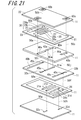
- FIG. 12 is a schematic exploded perspective view of the diplexer shown in FIG. 11. It is a top view which shows typically the upper and lower surfaces and interlayer of a diplexer shown in FIG.
- FIG. 12 is a cross-sectional view taken along the line PP ′ of FIG. 11. It is an external appearance perspective view which shows typically the diplexer of the 6th Embodiment of this invention.
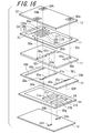
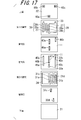
- FIG. 16 is a schematic exploded perspective view of the diplexer shown in FIG. 15. It is a top view which shows typically the upper and lower surfaces and interlayer of a diplexer shown in FIG.
- FIG. 16 is a cross-sectional view taken along the line QQ ′ of FIG.
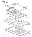
- FIG. 23 is a schematic exploded perspective view of the diplexer shown in FIG. 22.
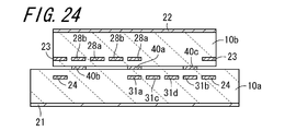
- FIG. 23 is a cross-sectional view taken along the line RR ′ of FIG. It is a figure which shows the simulation result of the electrical property of the diplexer of the 6th Embodiment of this invention.
- FIG. 1 is an exploded perspective view schematically showing an example of the structure of the composite resonator according to the first embodiment of the present invention.
- FIG. 2 is a plan view schematically showing the upper and lower surfaces and the layers of the composite resonator shown in FIG.
- the composite resonator constituting the bandpass filter of the present embodiment includes a first ground electrode 21, a second ground electrode 22, and a composite resonant electrode 26. .
- the laminate is formed by laminating a plurality of dielectric layers 11.
- the first ground electrode 21 is disposed on the lower surface of the multilayer body.
- the second ground electrode 22 is disposed on the upper surface of the stacked body.
- the composite resonance electrode 26 is disposed between the first layers of the multilayer body.
- the composite resonance electrode 26 includes a base 27 and a plurality of strip-shaped protrusions 28a and 28b. One end of the base 27 is grounded.
- the plurality of protrusions 28 a and 28 b are arranged side by side with one end connected to the other end of the base 27.
- One end of the base 27 becomes one end of the composite resonance electrode 26, and the other ends of the protrusions 28 a and 28 b become the other end of the composite resonance electrode 26.
- the whole of the base 27 and the protrusions 28a and 28b functions as a resonator that resonates at the first frequency
- the protrusions 28a and 28b It functions as a resonator that resonates at a second frequency higher than the frequency.
- An annular ground electrode 25 is disposed between the first layers of the multilayer body so as to surround the periphery of the composite resonance electrode 26, and one end of the composite resonance electrode 26 is connected to the annular ground electrode 25.
- the input coupling electrode 48a that opposes the electromagnetic coupling with the input stage protrusion 28a and the electromagnetic coupling with the output stage projection 28b.
- An output coupling electrode 48b is disposed.
- the input coupling electrode 48a and the output coupling electrode 48b are connected to the input terminal electrode 60a and the output terminal electrode 60d, which are disposed on the upper surface of the multilayer body through the through conductors 50a and 50d and spaced apart from the second ground electrode 22. Each is connected.
- the composite resonator having such a structure functions as a resonator in which the whole of the base 27 and the protrusions 28a and 28b are resonated at the first frequency by grounding one end, and the protrusion 28a. , 28b are provided with the composite resonance electrode 26 that functions as a resonator that resonates at a second frequency higher than the first frequency, thus functioning as a resonator having two resonance frequencies.
- one end of the composite resonance electrode 26 becomes a short-circuited end and the other end of the composite resonance electrode 26 becomes an open end, and the entire composite resonance electrode 26 functions as a quarter wavelength resonator.
- the projections 28a and 28b function as a quarter wavelength resonator. Conceivable.
- the composite resonator of this embodiment which has such a structure, since the one end connected to a ground potential inevitably becomes wide, a resonator having a high Q value can be obtained.
- the frequency difference between the first frequency and the second frequency can be arbitrarily controlled by the length of the protrusions 28a and 28b, the frequency difference between the first frequency and the second frequency is desired. Can be easily set. Therefore, by using this composite resonator, for example, a band-pass filter having a desired pass bandwidth, a dual mode oscillation circuit that oscillates at two desired frequencies, and the like can be easily configured. Therefore, for example, it becomes possible to easily configure a band pass filter having a very wide pass bandwidth that has been difficult to obtain with a band pass filter using a conventional quarter wavelength resonator.
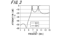
- FIG. 3 is a graph showing the simulation results of the electrical characteristics of the composite resonator having the structure shown in FIGS.
- the horizontal axis represents frequency
- the vertical axis represents attenuation.
- the pass characteristics (S21) and reflection characteristics of the composite resonator when the input terminal electrode 60a is port 1 and the output terminal electrode 60d is port 2 are shown. (S11) is shown. According to the graph shown in FIG.
- the composite resonant electrode 26 has a rectangular input stage having a width of 0.25 mm and a length of 2.0 mm at the other end of a rectangular base 27 having a width of 1.15 mm and a length of 1.05 mm.
- the protruding portion 28a and the protruding portion 28b of the output stage are arranged with a spacing of 0.65 mm.
- the input coupling electrode 48a and the output coupling electrode 48b have a rectangular shape with a width of 0.25 mm and a length of 1.0 mm, and the input stage protrusion 28a and the output stage protrusion 28b by a length of 0.2 mm. To face each other.
- the input terminal electrode 60a and the output terminal electrode 60d were square with sides of 0.3 mm.
- the outer shape of the first ground electrode 21, the second ground electrode 22, and the annular ground electrode 25 is a rectangular shape having a length of 5.0 mm and a width of 3.5 mm, and the opening of the annular ground electrode 25 has a width of 2
- a rectangular shape having a length of 0.7 mm and a length of 3.75 mm was used.
- the overall shape was a rectangular parallelepiped having a width of 5.0 mm, a length of 3.5 mm, and a thickness of 0.98 mm.
- the distance between the layer where the composite resonance electrode 26 is disposed and the layer where the input coupling electrode 48a and the output coupling electrode 48b are disposed is 0.065 mm.
- the thicknesses of the various electrodes were 0.01 mm, and the diameters of the through conductors 50a and 50d were 0.1 mm.
- the dielectric constant of the dielectric layer 11 was 9.45. In the composite resonator shown in FIGS.
- the composite resonant electrode 26 and the annular ground electrode 25 are disposed between the first layers of the multilayer body, and the first ground electrode 21 is disposed on the upper and lower surfaces of the multilayer body.
- the second ground electrode 22 and the second ground electrode 22 are disposed is shown, the second ground electrode 22 and the annular ground electrode 25 are not necessarily required, and the composite resonance electrode 26 may be disposed on the upper surface of the multilayer body.
- the input coupling electrode 48a and the output coupling electrode 48b may be disposed between the same layers as the composite resonance electrode. When a plurality of composite resonators are coupled, etc., On the other hand, either one is enough.
- the input terminal electrode 60a and the output terminal electrode 60d are not necessarily required.
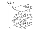
- FIG. 4 is an exploded perspective view schematically showing a bandpass filter according to a second embodiment of the present invention
- FIG. 5 is a plan view schematically showing the upper and lower surfaces and layers of the bandpass filter shown in FIG. .
- the bandpass filter of the present embodiment includes a laminate, a first ground electrode 21, a second ground electrode 22, a composite resonance electrode 26, and an annular ground electrode 25. It has.
- an input coupling electrode 40a that is electromagnetically coupled to face the projection 28a of the input stage and an output coupling electrode 40d that is electromagnetically coupled to the projection 28b of the output stage are arranged in the layer A of the laminate. Yes.
- the input coupling electrode 40a and the output coupling electrode 40d are connected to the input terminal electrode 60a and the output terminal electrode 60d, respectively, spaced from the second ground electrode 22 on the upper surface of the multilayer body through through conductors 50a and 50d. Has been.
- the electrical signal input point 45a of the input coupling electrode 40a is a connection point between the input coupling electrode 40a and the through conductor 50a
- the electrical signal output point 45d of the output coupling electrode 40d is a connection between the output coupling electrode 40d and the through conductor 50d. Is a point.
- the electric signal input point 45a is located closer to the other end of the composite resonance electrode 26 than the center of the portion facing the composite resonance electrode 26 in the input coupling electrode 40a.
- the electrical signal output point 45d is located closer to the other end of the composite resonance electrode 26 than the center of the portion facing the composite resonance electrode 26 in the output coupling electrode 40d.
- the band-pass filter of this embodiment having such a structure receives an input when an electric signal from an external circuit is input to the electric signal input point 45a of the input coupling electrode 40a via the input terminal electrode 60a and the through conductor 50a.
- the composite resonant electrode 26 that electromagnetically couples with the coupling electrode 40a resonates, and the electrical signal output point 45d of the output coupling electrode 40d that electromagnetically couples with the composite resonant electrode 26 passes through the through conductor 50d and the output terminal electrode 60d to an external circuit.
- An electrical signal is output.
- a signal in a frequency band including the first frequency and the second frequency at which the composite resonance electrode 26 resonates selectively passes, it functions as a band-pass filter.
- the bandpass filter of this embodiment functions as a resonator that resonates at the first frequency as a whole by combining the base 27 and the protrusions 28a and 28b, and the protrusions 28a and 28b are higher than the first frequency.
- a composite resonance electrode 26 that functions as a resonator that resonates at a frequency of 2 is provided. Therefore, the frequency difference between the first frequency and the second frequency can be controlled to some extent by the length of the protrusions 28a and 28b, so that a bandpass filter having a wide and desired passband can be easily obtained. Can get to.
- the band-pass filter of the present embodiment is electromagnetically coupled so as to face the protruding portion 28a of the input stage in the composite resonance electrode 26, which is disposed in a different layer from the layer in which the composite resonance electrode 26 of the multilayer body is disposed.
- the output coupling electrode 40d includes the output coupling electrode 40d, the input coupling electrode 40a, the output coupling electrode 40d, and the composite resonance electrode 26 are strongly electromagnetically coupled by broadside coupling, so that the flat and low loss is achieved over a wide passband.
- a bandpass filter having excellent pass characteristics can be obtained.
- the electric signal input point 45a is positioned closer to the other end of the composite resonance electrode 26 than the center of the portion facing the composite resonance electrode 26 in the input coupling electrode 40a.
- the electrical signal output point 45d is located closer to the other end of the composite resonance electrode 26 than the center of the opposed portion to the composite resonance electrode 26 in the output coupling electrode 40d.
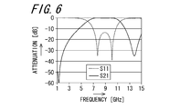
- FIG. 6 is a graph showing simulation results of electrical characteristics of the bandpass filter according to the second embodiment of the present invention having the structure shown in FIGS.
- the horizontal axis represents frequency
- the vertical axis represents attenuation.
- the bandpass filter pass characteristic (S21) and reflection characteristic when the input terminal electrode 60a is port 1 and the output terminal electrode 60d is port 2 are shown. (S11) is shown. According to the graph shown in FIG.
- the composite resonant electrode 26 has a rectangular shape with a width of 0.25 mm and a length of 2.0 mm at the other end of a rectangular base 27 having a width of 1.15 mm and a length of 1.05 mm.
- the projecting portion 28a at the input stage and the projecting portion 28b at the output stage are arranged with an interval of 0.65 mm.
- the input coupling electrode 40a and the output coupling electrode 40d have a rectangular shape with a width of 0.25 mm and a length of 3.0 mm.
- the input terminal electrode 60a and the output terminal electrode 60d were square with sides of 0.3 mm.
- the outer shape of the first ground electrode 21, the second ground electrode 22, and the annular ground electrode 25 is a rectangular shape having a length of 5.0 mm and a width of 3.5 mm, and the opening of the annular ground electrode 25 has a width of 2
- a rectangular shape having a length of 0.7 mm and a length of 3.75 mm was used.
- the overall shape of the bandpass filter was a rectangular parallelepiped having a width of 5.0 mm, a length of 3.5 mm, and a thickness of 0.98 mm, and the composite resonance electrode 26 was positioned in the center in the thickness direction.
- the distance between the layer where the composite resonance electrode 26 is disposed and the layer where the input coupling electrode 40a and the output coupling electrode 40d are disposed is 0.065 mm.
- the thicknesses of the various electrodes were 0.01 mm, and the diameters of the through conductors 50a and 50d were 0.1 mm.
- the dielectric constant of the dielectric layer 11 was 9.45. Further, in the bandpass filter of the present embodiment shown in FIGS. 4 and 5, an example in which the input coupling electrode 40a, the output coupling electrode 40d, and the composite resonance electrode 26 are arranged so as to be electromagnetically coupled in an interdigital manner.
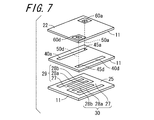
- FIG. 7 is an exploded perspective view schematically showing a bandpass filter according to a third embodiment of the present invention
- FIG. 8 is a plan view schematically showing the upper and lower surfaces and layers of the bandpass filter shown in FIG. .
- FIGS. 1-10 only differences from the above-described second embodiment will be described, and the same components will be denoted by the same reference numerals and redundant description will be omitted. As shown in FIGS.
- the band-pass filter of this embodiment includes an input stage composite resonance electrode 29 and an output stage composite resonance electrode having the same structure and function as the composite resonance electrode 26 of the second embodiment.
- 30 are arranged side by side so that one end and the other end thereof are staggered between the first layers of the multilayer body and are electromagnetically coupled to each other, and the protrusions of the input stage in the composite resonance electrode 29 of the input stage
- the input coupling electrode 40a is disposed so as to be opposed to the electromagnetic field 28a
- the output coupling electrode 40d is disposed so as to be opposed to the output stage protrusion 28b of the composite resonance electrode 30 of the output stage. ing.
- the band-pass filter of this embodiment having such a structure receives an input when an electric signal from an external circuit is input to the electric signal input point 45a of the input coupling electrode 40a via the input terminal electrode 60a and the through conductor 50a.
- the input stage composite resonance electrode 29 that electromagnetically couples with the coupling electrode 40a and the output stage composite resonance electrode 30 that electromagnetically couples with the coupling electrode 40a resonates, and the output coupling electrode 40d that electromagnetically couples with the output stage composite resonance electrode 30
- An electrical signal is output from the electrical signal output point 45d to an external circuit through the through conductor 50d and the output terminal electrode 60d.
- the band-pass filter of this embodiment includes a plurality of composite resonance electrodes 29 and 30 that are arranged side by side so that one end and the other end thereof are staggered between the first layers of the multilayer body and are electromagnetically coupled to each other. Prepare. Thereby, many resonance peaks can be obtained according to the number of composite resonance electrodes.
- the composite resonance electrodes 29 and 30 are electromagnetically coupled to each other in an interdigital manner, the coupling due to the magnetic field and the coupling due to the electric field are added and strongly coupled to each other.
- the frequency interval can be increased. With these effects, a bandpass filter having a very wide passband can be easily obtained.
- the bandpass filter of the present embodiment is opposed to the input stage protrusion 28a in the composite resonance electrode 29 of the input stage, which is disposed in a different layer from the layer in which the multilayer composite resonance electrodes 29 and 30 are disposed.
- the projecting portion of the output stage in the composite resonant electrode 30 of the output stage which is disposed in a layer different from the layer in which the composite resonant electrodes 29 and 30 of the laminated body are disposed, and the strip-shaped input coupled electrode 40a to be electromagnetically coupled.
- a band-shaped output coupling electrode 40d that is electromagnetically coupled to face 28b.
- the input coupling electrode 40a and the input stage composite resonance electrode 29 are strongly electromagnetically coupled by broadside coupling, and the output coupling electrode 40d and the output stage composite resonance electrode 30 are strongly electromagnetically coupled by broadside coupling. Therefore, it is possible to obtain a bandpass filter having a flat and low-loss pass characteristic over the entire very wide passband. Furthermore, according to the bandpass filter of the present embodiment, the electric signal input point 45a is connected to the other of the composite resonance electrode 29 in the input stage than the center of the input coupling electrode 40a facing the composite resonance electrode 29 in the input stage.
- the electrical signal output point 45d is located closer to the end of the output coupling electrode 40d and closer to the other end of the composite resonance electrode 30 at the output stage than the center of the output coupling electrode 40d facing the composite resonance electrode 30 at the output stage. Located on the side.
- the input coupling electrode 40a and the composite resonance electrode 29 at the input stage are electromagnetically coupled in an interdigital manner, so that the coupling due to the magnetic field and the coupling due to the electric field are added, and the electromagnetic coupling is strongly performed.
- the coupling electrode 40d and the composite resonance electrode 30 at the output stage are electromagnetically coupled in an interdigital manner, the coupling due to the magnetic field and the coupling due to the electric field are added and strongly coupled to each other.
- FIG. 9 is a plan view schematically showing the upper and lower surfaces and the layers of the bandpass filter according to the fourth embodiment of the present invention.
- the band-pass filter of this embodiment is located between the input stage protrusion 28a and the output stage protrusion 28b of the input stage composite resonance electrode 29 and the output stage composite resonance electrode 30.
- the portion is provided with a structure in which a plurality of through conductors 50 t are arranged so as to penetrate the multilayer body and both ends are connected to the first ground electrode 21 and the second ground electrode 22.
- the bandpass filter of the present embodiment having such a structure, the direct electromagnetic coupling between the input coupling electrode 40a and the output coupling electrode 40d can be made very small by the grounded through conductor 50t. Therefore, it is possible to obtain a bandpass filter having excellent pass characteristics with increased attenuation in a frequency region other than the passband.
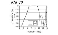
- FIG. 10 shows the electrical characteristics of the bandpass filter (BPF2) of the third embodiment having the structure shown in FIGS. 7 and 8, and the bandpass filter (BPF3) of the fourth embodiment having the structure shown in FIG.
- the composite resonant electrode 29 at the input stage and the composite resonant electrode 30 at the output stage are long at a width of 0.25 mm at the other end of the rectangular base portion 27 having a width of 1.05 mm and a length of 0.9 mm.
- a rectangular input stage protrusion 28a and an output stage protrusion 28b having a length of 2.15 mm are arranged with an interval of 0.6 mm so that one end and the other end of each are staggered. Were arranged side by side with an interval of 0.21 mm.
- the input coupling electrode 40a and the output coupling electrode 40d have a rectangular shape with a width of 0.25 mm and a length of 3.0 mm.
- the input terminal electrode 60a and the output terminal electrode 60d were square with sides of 0.3 mm.
- the outer shapes of the first ground electrode 21, the second ground electrode 22, and the annular ground electrode 25 are rectangular shapes having a length of 5.0 mm and a width of 4.5 mm, and the opening of the annular ground electrode 25 has a width of 3 mm.
- the rectangular shape was 7 mm and the length was 3.25 mm.
- the overall shape of the bandpass filter was a rectangular parallelepiped having a length of 5.0 mm, a width of 4.5 mm, and a thickness of 0.98 mm, and the composite resonance electrodes 29 and 30 were positioned in the center in the thickness direction.
- the distance between the layers where the composite resonance electrodes 29 and 30 are disposed and the layer where the input coupling electrode 40a and the output coupling electrode 40d are disposed is 0.065 mm.
- the thicknesses of the various electrodes were 0.01 mm, and the diameters of the through conductors 50a, 50d, and 50t were 0.1 mm.
- the dielectric constant of the dielectric layer 11 was 9.45. (Fifth embodiment) FIG.
- FIG. 11 is an external perspective view schematically showing a diplexer according to a fifth embodiment of the present invention.
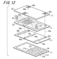
- FIG. 12 is a schematic exploded perspective view of the diplexer shown in FIG.
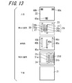
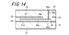
- FIG. 13 is a plan view schematically showing the upper and lower surfaces and layers of the diplexer shown in FIG. 14 is a cross-sectional view taken along the line PP ′ of FIG.
- the diplexer of the present embodiment includes a laminate 10, a first ground electrode 21, a second ground electrode 22, a plurality of composite resonance electrodes 29 and 30, and a band-like shape.
- a plurality of single resonance electrodes 31a, 31b, 31c, and 31d are provided.
- Each of the composite resonance electrodes 29 and 30 is grounded at one end, so that the whole of the base 27 and the protrusions 28a and 28b functions as a resonator that resonates at the first frequency, and the protrusions 28a and 28b. Functions as a resonator that resonates at a second frequency higher than the first frequency.
- the plurality of composite resonance electrodes 29 and 30 are arranged side by side so that one end and the other end thereof are alternated between the first layers of the laminate 10 and are electromagnetically coupled to each other.
- the plurality of single resonance electrodes 31a, 31b, 31c, 31d are arranged side by side so as to be electromagnetically coupled to each other in a second layer different from the first layer of the laminate 10, and one end of each is grounded. And function as a resonator that resonates at a third frequency different from the first frequency and the second frequency.
- the third frequency is set lower than the first frequency.
- the diplexer of the present embodiment includes a strip-shaped input coupling electrode 40a, a strip-shaped first output coupling electrode 40b, and a strip-shaped second output coupling electrode 40c.
- the input coupling electrode 40 a is disposed in the interlayer A located between the first layer and the second layer of the multilayer body 10, and in the composite resonance electrode 29 in the input stage among the plurality of composite resonance electrodes 29 and 30.
- the single-stage resonant electrode 31a of the input stage among the plurality of single-resonance electrodes 31a, 31b, 31c, and 31d is electromagnetically coupled to the projection-stage 28a of the input stage among the plurality of projections 28a, 28b.
- an electric signal input point 45a to which an electric signal is input.
- the first output coupling electrode 40 b is disposed in an interlayer A different from the first interlayer of the multilayer body 10, and the plurality of protrusions 28 a in the composite resonance electrode 30 at the output stage among the plurality of composite resonance electrodes 29 and 30. , 28b, the first electric signal output point 45b is connected to the projecting portion 28b of the output stage so as to face the electromagnetic field coupling and output an electric signal.
- the second output coupling electrode 40c is disposed in an interlayer A different from the second interlayer of the multilayer body 10, and includes a single resonance electrode 31b in the output stage among the plurality of single resonance electrodes 31a, 31b, 31c, and 31d. A second electric signal output point 45c is provided which is opposed to the electromagnetic field and outputs an electric signal.
- the diplexer according to the present embodiment is formed in an annular shape so as to surround the plurality of composite resonance electrodes 29 and 30 between the first layers of the multilayer body 10, and one ends of the plurality of composite resonance electrodes 29 and 30 are connected.
- the first annular ground electrode 23 is formed in an annular shape so as to surround the plurality of single resonance electrodes 31a, 31b, 31c, 31d between the second layers, and the plurality of single resonance electrodes 31a, 31b, And a second annular ground electrode 24 to which one end of 31c, 31d is connected.
- the input coupling electrode 40a is connected to the input terminal electrode 60a disposed on the upper surface of the multilayer body 10 through the through conductor 50a
- the first output coupling electrode 40b is connected to the multilayer body 10 through the through conductor 50b
- the second output coupling electrode 40c is connected to the first output terminal electrode 60c disposed on the upper surface of the multilayer body 10 through the through conductor 50c. It is connected. Therefore, a connection point between the input coupling electrode 40a and the through conductor 50a becomes an electric signal input point 45a where an electric signal is input to the input coupling electrode 40a, and a connection point between the first output coupling electrode 40b and the through conductor 50b.
- the plurality of composite resonance electrodes 29 and 30 that are electromagnetically coupled to each other By exciting the input stage composite resonance electrode 29 that is electromagnetically coupled to the electrode 40a, the plurality of composite resonance electrodes 29 and 30 that are electromagnetically coupled to each other resonate, and the output stage composite resonance electrode 30 and the electromagnetic field coupling are resonated.
- An electric signal is output from the first electric signal output point 45b of the first output coupling electrode 40b to the external circuit through the through conductor 50b and the first output terminal electrode 60b.
- the signal in the first frequency band including the frequency at which the plurality of composite resonance electrodes 29 and 30 resonate selectively passes the first pass band is thereby formed.
- the input coupling electrode 40a and the electromagnetic wave When the single resonance electrode 31a of the input stage that is coupled to the field is excited, a plurality of single resonance electrodes 31a, 31b, 31c, and 31d that are electromagnetically coupled to each other resonate, and the single resonance electrode 31b of the output stage An electric signal is output from the second electric signal output point 45c of the second output coupling electrode 40c to be electromagnetically coupled to the external circuit through the through conductor 50c and the second output terminal electrode 60c.
- the diplexer of this embodiment functions as a diplexer that demultiplexes the signal input from the input terminal electrode 60a according to the frequency and outputs the demultiplexed signal from the first output terminal electrode 60b and the second output terminal electrode 60c.
- the first ground electrode 21 is disposed on the entire lower surface of the multilayer body 10
- the second ground electrode 22 is the input terminal electrode 60 a and the first output terminal on the upper surface of the multilayer body 10.
- the electrodes 60b and the second output terminal electrode 60c are arranged on almost the entire surface except for the periphery, and both are grounded, and a plurality of composite resonance electrodes 29, 30 and a plurality of single resonance electrodes 31a, 31b, 31c, A stripline resonator is formed together with 31d. Further, the first annular ground electrode 23 and the second annular ground electrode 24 are grounded, so that one ends of the composite resonance electrodes 29, 30 and the plurality of single resonance electrodes 31a, 31b, 31c, 31d are provided. Is grounded, and also has a function of suppressing leakage of electromagnetic waves generated from the composite resonance electrodes 29 and 30 and the plurality of single resonance electrodes 31a, 31b, 31c, and 31d to the surroundings.
- the composite resonance electrodes 29 and 30 are basically grounded at one end (that is, one end of the base 27), so that the entire base 27 and protrusions 28a and 28b are basically combined at the first frequency. While functioning as a 1 ⁇ 4 wavelength resonator that resonates, the protrusions 28a and 28b function as a 1 ⁇ 4 wavelength resonator that resonates at a second frequency higher than the first frequency. Therefore, the total length of the base 27 and the protrusions 28a and 28b is substantially equal to 1 ⁇ 4 of the wavelength at the first frequency, and the length of the protrusions 28a and 28b is equal to the wavelength at the second frequency.
- the lengths of the projections 28a and the projections 28b are basically set equal to each other, but it may be preferable that the lengths are slightly different depending on the coupling state with other electrodes.
- the number of protrusions may be three or more, but it is better to use two for miniaturization.
- a plurality of strip-shaped single resonance electrodes 31a, 31b, 31c, and 31d are quarter-wave resonators that resonate at the third frequency by having one end connected to the second annular ground electrode 24 and grounded. Function as.
- Each electrical length is set to about 1 ⁇ 4 of the wavelength at the third frequency.
- the plurality of composite resonance electrodes 29 and 30 are arranged side by side between the first layers of the multilayer body 10 and are edge-coupled to each other, and the plurality of single resonance electrodes 31a, 31b, 31c, and 31d are stacked. They are arranged side by side between the second layers of the body 10 and are edge-coupled to each other.
- it is set to about 0.05 to 0.5 mm.
- the distance between the input coupling electrode 40a and the composite resonance electrode 29 at the input stage and the single resonance electrode 31a at the input stage, the distance between the first output coupling electrode 40b and the composite resonance electrode 30 at the output stage, and the second The distance between the output coupling electrode 40c and the single resonance electrode 31b at the output stage is set to, for example, about 0.01 to 0.5 mm because the coupling becomes stronger but the manufacturing becomes difficult if the distance is reduced.
- the entirety of the base 27 and the protrusions 28a and 28b functions as a resonator that resonates at the first frequency, and the protrusions 28a and 28b are higher than the first frequency.
- the composite resonance electrodes 29 and 30 functioning as resonators that resonate at the frequency of 2 are provided, the frequency difference between the first frequency and the second frequency is arbitrarily controlled to some extent by the length of the protrusions 28a and 28b. Therefore, the width of the pass band formed by the composite resonance electrodes 29 and 30 can be easily set to a wide and desired width. Further, according to the diplexer of the present embodiment, the plurality of composite resonance electrodes 29 and 30 are arranged side by side between the first layers of the multilayer body 10 such that one end and the other end thereof are staggered, and electromagnetically mutually.
- the plurality of composite resonance electrodes 29 and 30 are electromagnetically coupled to each other in an interdigital manner. Is added to strongly electromagnetically couple each other, so that the frequency interval between the respective resonance peaks can be increased, so that the width of the pass band formed by the composite resonance electrodes 29 and 30 is very wide. can do.
- the input coupling electrode 40a that couples the input stage protrusion 28a in the composite resonance electrode 29 of the input stage and the dielectric layer 11 to face each other with the electromagnetic coupling therebetween, and the output stage In the composite resonance electrode 30, the output stage protrusion 28 b and the first output coupling electrode 40 b that are opposed to each other with the dielectric layer 11 interposed therebetween are electromagnetically coupled.
- the composite resonance electrode 29 is strongly electromagnetically coupled by broadside coupling
- the first output coupling electrode 40b and the output stage composite resonance electrode 30 are strongly electromagnetically coupled by broadside coupling.
- the electrical signal input point 45a is located at the other end of the composite resonance electrode 29 at the input stage than at the center of the input coupling electrode 40a facing the composite resonance electrode 29 at the input stage.
- the first electric signal output point 45b is positioned closer to the output stage than the center of the first output coupling electrode 40b facing the composite resonance electrode 30 at the output stage. Since the input coupling electrode 40a and the composite resonance electrode 29 in the input stage are electromagnetically coupled in an interdigital manner, the coupling by the magnetic field and the coupling by the electric field are added. Then, the first output coupling electrode 40b and the composite resonance electrode 30 of the output stage are electromagnetically coupled to each other in an interdigital type, thereby coupling the magnetic field and the electric field.
- the diplexer of the present embodiment since one end of the composite resonance electrode 29 in the input stage and one end of the single resonance electrode 31a in the input stage are located on the same side, the input is thus performed.
- the coupling electrode 40a, the composite resonance electrode 29 at the input stage, and the single resonance electrode 31a at the input stage can be broadside-coupled and coupled in an interdigital manner.
- the electric signal input point 45a is located at the input coupling electrode 40a of the single resonance electrode 31a of the input stage rather than the center of the opposed portion of the input coupling electrode 40a to the single resonance electrode 31a of the input stage.
- the second electrical signal output point 45c is located on the side close to the other end, and the second electrical signal output point 45c has a single output stage than the center of the second output coupling electrode 40c facing the single resonance electrode 31b of the output stage. Since the input coupling electrode 40a and the input stage single resonance electrode 31a are electromagnetically coupled in an interdigital manner, the magnetic field coupling and the electric field are located.
- the first output coupling electrode 40b and the single resonance electrode 31b of the output stage are electromagnetically coupled to each other by the interdigital type. And the coupling due to the electric field are added and strongly electromagnetically coupled to each other, so that the flat and low level can be achieved over the entire very wide passband formed by the plurality of single resonance electrodes 31a, 31b, 31c, 31d. A diplexer having lossy passing characteristics can be obtained. Still further, according to the diplexer of the present embodiment, the first output coupling electrode 40b and the second output coupling electrode 40b, which are generated when the composite resonance electrodes 29, 30 and the single resonance electrodes 31a, 31b, 31c, 31d are directly electromagnetically coupled.
- the composite resonant electrodes 29, 30 and the single resonant electrodes 31a, 31b, 31c, 31d are different in shape, so that the composite resonant electrodes 29, 30 and the single resonant electrodes 31a, 31b, 31c, 31d are mutually connected. This may be because the electromagnetic field coupling is difficult.
- the first output coupling electrode 40b and the second output coupling electrode 40c are positioned on opposite sides of the input coupling electrode 40a when viewed in plan.
- FIG. 15 is an external perspective view schematically showing a diplexer according to a sixth embodiment of the present invention. 16 is a schematic exploded perspective view of the diplexer shown in FIG. FIG.
- the input coupling electrode 40a includes a strip-shaped first input coupling conductor 41a, a strip-shaped second input coupling conductor 42a, and an input-side connection conductor. 43a and input side connection auxiliary conductor 44a.
- the first input coupling conductor 41a is disposed in the interlayer A located between the first layer and the second layer of the multilayer body 10, and faces the single resonance electrode 31a in the input stage.
- the second input coupling conductor 42 a is disposed in the layer B located between the first layer and the layer A of the multilayer body 10, and faces the projection 28 a of the input stage of the composite resonance electrode 29 of the input stage.
- the input side connection conductor 43a and the input side connection auxiliary conductor 44a connect the first input coupling conductor 41a and the second input coupling conductor 42a.
- the distance between the input coupling electrode 40a and the input stage composite resonance electrode 29 and the input stage single resonance electrode 31a is maintained.
- the interval between the composite resonance electrode 29 at the input stage and the single resonance electrode 31a at the input stage can be increased. Therefore, the single resonance of the input stage composite resonance electrode 29 and the input stage single resonance without weakening the electromagnetic coupling between the input coupling electrode 40a and the input stage composite resonance electrode 29 and the input stage single resonance electrode 31a. Direct electromagnetic coupling with the electrode 31a can be weakened.
- the electromagnetic coupling between the input coupling electrode 40a and the composite resonance electrode 29 at the input stage and the single resonance electrode 31a at the input stage can be further strengthened.
- the electric signal input point 45a is arranged on the opposite side of the input side connection conductor 43a from the center of the opposing region of the first input coupling conductor 41a and the second input coupling conductor 42a. Therefore, the electromagnetic coupling between the input coupling electrode 40a and the composite resonance electrode 29 of the input stage and the single resonance electrode 31a of the input stage can be further strengthened.
- This mechanism is based on the fact that the first input coupling conductor 41a and the second input coupling conductor 42a are connected by the input side connection auxiliary conductor 44a, so that the first input coupling conductor 41a is near the open end of the input coupling electrode 40a. Since the potential difference between the first input coupling conductor 42a and the second input coupling conductor 42a is small, the electromagnetic coupling between the first input coupling conductor 41a and the second input coupling conductor 42a is small. This is because the electromagnetic field coupling between the conductor 41a and the input stage single resonance electrode 31a is strengthened, and the electromagnetic field coupling between the second input coupling conductor 42a and the input stage composite resonance electrode 29 is strengthened. Presumed to be.
- the input side connection auxiliary conductor 44a is connected to the electric signal input point 45a and the input side with respect to the center in the region where the first input coupling conductor 41a and the second input coupling conductor 42a are opposed to each other. Since the connection conductor 43a is disposed at the end opposite to the side where the connection conductor 43a is disposed, between the first input coupling conductor 41a and the second input coupling conductor 42a in the vicinity of the open end of the input coupling electrode 40a. Therefore, the electromagnetic field coupling between the input coupling electrode 40a and the composite resonance electrode 29 of the input stage and the single resonance electrode 31a of the input stage can be further strengthened.
- the input side connection conductor 43a and the input side connection auxiliary conductor 44a are disposed at both ends of the opposing region of the first input coupling conductor 41a and the second input coupling conductor 42a. Therefore, the potentials of the first input coupling conductor 41a and the second input coupling conductor 42 can be made close to each other over the entire opposing region, so that the input coupling electrode 40a and the input stage composite resonance electrode 29 and The electromagnetic coupling between the input stage and the single resonance electrode 31a can be further enhanced.
- an input stage resonance auxiliary electrode 32 a and an output stage resonance auxiliary electrode 32 b are arranged between the layers A of the multilayer body 10.
- the resonance auxiliary electrode 32a at the input stage is disposed so as to have a region facing the second annular ground electrode 24, and is connected to the open end of the single resonance electrode 31a at the input stage via the through conductor 50e.
- the output stage resonance auxiliary electrode 32b is disposed so as to have a region facing the second annular ground electrode 24, and is connected to the open end of the output stage single resonance electrode 31b via a through conductor 50f.
- Resonance auxiliary electrodes 32c and 32d are arranged in the interlayer C located below the first interlayer of the multilayer body 10.
- the resonance auxiliary electrodes 32c and 32d are arranged so as to have a region facing the second annular ground electrode 24, and are connected to the other ends of the single resonance electrodes 31c and 31d by through conductors 50g and 50h, respectively.
- capacitance is generated between the resonance auxiliary electrodes 32a, 32b, 32c, and 32d and the second annular ground electrode 24, and the resonance auxiliary electrodes 32a, 32b, and 32c.
- 32d is added to the capacitance between the single resonant electrodes 31a, 31b, 31c, 31d connected to the ground potential and the length of each of the single resonant electrodes 31a, 31b, 31c, 31d.
- a small diplexer can be obtained.
- the area of the facing portion between the resonance auxiliary electrodes 32a, 32b, 32c, and 32d and the second annular ground electrode 24 is, for example, 0.01 to 3 mm from the balance between the required size and the obtained capacitance. 2 Set to degree. A smaller capacitance between the opposing portions of the resonance auxiliary electrodes 32a, 32b, 32c, and 32d and the second annular ground electrode 24 can generate a larger capacitance, but it is difficult to manufacture. It is set to about 01 to 0.5 mm.
- the diplexer according to the present embodiment includes an input coupling auxiliary electrode 46a and an output coupling auxiliary electrode 46b in an interlayer B located above the interlayer A of the multilayer body 10.
- the input coupling auxiliary electrode 46a is disposed so as to have a region facing the resonance auxiliary electrode 32a in the input stage, and an electric signal input point of the first input coupling conductor 41a constituting the input coupling electrode 40a via the through conductor 50i. 45a.
- the output coupling auxiliary electrode 46b is disposed so as to have a region facing the resonance auxiliary electrode 32b of the output stage, and is connected to the second electric signal output point 45c of the second output coupling electrode 40c through the through conductor 50j.
- the input coupling auxiliary electrode 46a is connected to the input terminal electrode 60a through the through conductor 50a, and the output coupling auxiliary electrode 46b is connected to the second output terminal electrode 60c through the through conductor 50c.
- the electromagnetic coupling generated between the resonance auxiliary electrode 32a at the input stage and the input coupling auxiliary electrode 46a is added to the electromagnetic coupling between the single resonance electrode 31a at the input stage and the input coupling electrode 40a. Is done.
- the electromagnetic coupling generated between the resonance auxiliary electrode 32b at the output stage and the output coupling auxiliary electrode 46b is the electromagnetic coupling between the single resonance electrode 31b at the output stage and the second output coupling electrode 40c. Is added to As a result, the electromagnetic coupling between the input coupling electrode 40a and the input stage single resonance electrode 31a and the electromagnetic coupling between the second output coupling electrode 40c and the output stage single resonance electrode 31b are further strengthened. be able to.
- the input coupling electrode 40a, the input stage composite resonance electrode 29, and the input stage single resonance electrode 31a are very strongly electromagnetically coupled, and the first output coupling electrode 40b and the composite resonance electrode 30 at the output stage are very strongly electromagnetically coupled, and the second output coupling electrode 40c and the single resonance electrode 31b at the output stage are extremely strongly electromagnetically coupled.
- the widths of the input coupling auxiliary electrode 46a and the output coupling auxiliary electrode 46b are set to be approximately the same as, for example, the input coupling electrode 40a and the second output coupling electrode 40c.
- the smaller distances between the input coupling auxiliary electrode 46a and the output coupling auxiliary electrode 46b and the resonance auxiliary electrodes 32a and 32b are desirable in terms of causing strong coupling, but the manufacturing becomes difficult. It is set to about 0.5 mm. (Seventh, eighth and ninth embodiments) FIG.
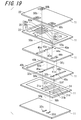
- FIG. 19 is an exploded perspective view schematically showing a diplexer according to a seventh embodiment of the present invention
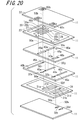
- FIG. 20 is an exploded perspective view schematically showing a diplexer according to an eighth embodiment of the present invention.
- These are the disassembled perspective views which show typically the diplexer of the 9th Embodiment of this invention.
- the same components will be denoted by the same reference numerals, and redundant description will be omitted.
- all of the single resonance electrodes 31a, 31b, 31c, and 31d are coupled in a comb line type with one end and the other end aligned on the same side. Are arranged side by side.
- the single resonance electrode 31a and the single resonance electrode 31c are coupled in an interdigital manner, and the single resonance electrode 31c and the single resonance electrode 31d are combline type.
- the single resonance electrode 31d and the single resonance electrode 31b are arranged side by side so as to be coupled in an interdigital manner.
- the single resonance electrode 31a and the single resonance electrode 31c are coupled in a comb line type, and the single resonance electrode 31c and the single resonance electrode 31d are interdigital.
- the single resonance electrode 31d and the single resonance electrode 31b are arranged side by side so as to be coupled to the combline type coupling.
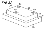
- FIG. 22 is an external perspective view schematically showing a diplexer according to a tenth embodiment of the present invention.
- FIG. 23 is a schematic exploded perspective view of the diplexer shown in FIG. 24 is a cross-sectional view taken along the line RR ′ of FIG.
- the laminated body is composed of the first laminated body 10a and the second laminated body 10b arranged thereon, and the first ground electrode 21 is disposed on the lower surface of the first laminated body 10a, the second ground electrode 22 is disposed on the upper surface of the second laminated body 10b, and the composite resonant electrodes 29 and 30 and the first annular ground electrode 23 is a layer in the second laminated body 10b, and a second layer in which the single resonant electrodes 31a, 31b, 31c, 31d and the second annular ground electrode 24 are disposed is Between the layers in the first laminate 10a, the input coupling electrode 40a, the first output coupling electrode 40b, and the second output coupling electrode 40c are between the first laminate 10a and the second laminate 10b.
- the first stacked body 10a is configured by stacking a plurality of dielectric layers 11a
- the second stacked body 10b is configured by stacking a plurality of dielectric layers 11b.
- the region where the composite resonance electrodes 29 and 30 and the single resonance electrodes 31a, 31b, 31c and 31d having different resonance frequencies are arranged is the input coupling electrode 40a.
- the first stacked body 10a and the second stacked body 10b are separated from each other at the boundary between the first output coupling electrode 40b and the second output coupling electrode 40c. It is possible to easily obtain desired electrical characteristics by making the physical properties of the dielectric layers constituting the 10a and the second laminated body 10b different.
- the dielectric constant of the dielectric layer 11a constituting the first laminated body 10a in which the single resonance electrodes 31a, 31b, 31c, 31d longer than the composite resonance electrodes 29, 30 are arranged is given by Since the length of the single resonance electrodes 31a, 31b, 31c, and 31d can be shortened by setting the dielectric constant higher than the dielectric constant of the dielectric layer 11b constituting the second laminated body 10b, wasted space in the diplexer. The diplexer can be reduced in size by eliminating the above.
- the diplexer according to the present embodiment is configured such that the electromagnetic waves between the electrodes arranged separately on the upper and lower sides with the interlayer where the input coupling electrode 40a, the first output coupling electrode 40b, and the second output coupling electrode 40c are arranged therebetween. Since the structure does not require the field coupling, the first stacked body 10a and the second stacked body are separated from each other with the layer where the input coupling electrode 40a, the first output coupling electrode 40b, and the second output coupling electrode 40c are disposed. When the position difference occurs between the first stacked body 10a and the second stacked body 10b by dividing into the stacked body 10b, or the boundary between the first stacked body 10a and the second stacked body 10b.
- the first laminated body 10a is a module substrate on which other electronic components or the like are mounted on the surface of a region other than the region where the diplexer is formed, a part of the diplexer is a second laminated layer.
- the thickness of the module substrate can be reduced, so that a substrate with a diplexer that can reduce the thickness of the entire module can be obtained.
- the electrical characteristics of the diplexer of the sixth embodiment shown in FIGS. 15 to 18 were calculated by simulation using the finite element method.
- the composite resonant electrode 29 at the input stage and the composite resonant electrode 30 at the output stage have a width of 0.25 mm at the other end of the rectangular base portion 27 having a width of 1.05 mm and a length of 0.95 mm.
- a rectangular input stage protrusion 28a having a length of 2.1 mm and a rectangular output stage protrusion 28b having a width of 0.2 mm and a length of 2.25 mm are arranged at an interval of 0.6 mm. And arranged side by side at an interval of 0.25 mm so that one end and the other end of each other are staggered.
- the single resonance electrodes 31a, 31b, 31c, and 31d have a rectangular shape with a width of 0.3 mm and a length of 3.6 mm, and the distance between the single resonance electrodes 31a and 31c is 0.2 mm.
- the distance between 31c and 31d was 0.27 mm, and the distance between the single resonance electrodes 31d and 31b was 0.2 mm.
- the resonance auxiliary electrode 32a at the input stage and the resonance auxiliary electrode 32b at the output stage are 0.45 mm wide and 0.49 mm long, respectively, placed 0.2 mm away from the other ends of the single resonance electrodes 31a and 31b. And a rectangle having a width of 0.2 mm and a length of 0.5 mm toward the single resonance electrodes 31a and 31b.
- the other resonance auxiliary electrodes 32c and 32d are a rectangle having a width of 0.47 mm and a length of 0.5 mm arranged at a distance of 0.2 mm from the other ends of the single resonance electrodes 31c and 31d, respectively, and a single A rectangular shape having a width of 0.2 mm toward the resonance electrodes 31 c and 31 d and a length of 0.5 mm was joined.
- the first input coupling conductor 41a has a rectangular end with a width of 0.25 mm and a length of 3.7 mm, and an extension portion with a width of 0.45 mm and a length of 0.4 mm is added to adjust the coupling. Shaped.
- the second input coupling conductor 42a has a rectangular tip having a width of 0.25 mm and a length of 2.6 mm, and an extension portion having a width of 0.45 mm and a length of 0.4 mm is added to adjust the coupling. Shaped. Then, the first input coupling conductor 41a and the second input coupling conductor 42a were connected by the input side connection conductor 43a and the input side connection auxiliary conductor 44a formed of via holes to form the input coupling electrode 40a.
- the first output coupling electrode 40b and the second output coupling electrode 40c were rectangular with a width of 0.25 mm and a length of 3.2 mm.
- the input coupling auxiliary electrode 46a and the output coupling auxiliary electrode 46b have a rectangular shape with a width of 0.25 mm and a length of 1.1 mm.
- the input terminal electrode 60a, the first output terminal electrode 60b, and the second output terminal electrode 60c were squares with a side of 0.3 mm.
- the outer shapes of the first ground electrode 21, the second ground electrode 22, the first annular ground electrode 23 and the second annular ground electrode 24 are 5 mm wide and 6 mm long.
- the opening has a rectangular shape with a width of 3.75 mm and a length of 4.9 mm, and the opening of the second annular ground electrode 24 has a rectangular shape with a width of 3.25 mm and a length of 3.9 mm.
- the overall shape of the diplexer was a rectangular parallelepiped shape having a width of 5 mm, a length of 6 mm, and a thickness of 0.98 mm, and the interlayer B was positioned substantially at the center in the thickness direction.
- the distance between adjacent layers among the first layer, the second layer, the layer A, the layer B, and the layer C was 0.065 mm.
- the thicknesses of the various electrodes were 0.01 mm, and the diameters of the various through conductors were 0.1 mm.
- the dielectric constant of the dielectric layer 11 was 9.45.
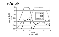
- FIG. 25 is a graph showing the simulation results.
- FIG. 26 shows the sixth embodiment shown in FIGS.
- S32 is about ⁇ 20 dB, which shows that there is room for improvement in the isolation characteristics of the diplexer of the comparative example.
- S32 is about ⁇ 35 dB at a frequency of about 3 to 5 GHz in the vicinity of the passband formed by the single resonance electrodes 31a, 31b, 31c, and 31d. Compared with the graph shown in FIG. 5, the improvement is 15 dB or more, and a very good isolation characteristic is obtained.
- FIG. 27 is a block diagram showing a configuration example of a wireless communication module 80 and a wireless communication device 85 using a bandpass filter according to the eleventh embodiment of the present invention.
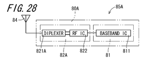
- FIG. 28 is a block diagram showing a configuration example of a wireless communication module 80A and a wireless communication device 85A using a diplexer according to the twelfth embodiment of the present invention.
- the wireless communication module 80 (80A) of the present embodiment includes, for example, a baseband unit 81 where a baseband signal is processed, and an RF signal which is connected to the baseband unit 81 and after modulation of the baseband signal and before demodulation is processed.
- RF section 82 (82A) The RF unit 82 includes the band-pass filter 821 (diplexer 821A) of the present invention described above, and the band-pass filter 821 transmits a signal other than the communication band in the RF signal obtained by modulating the baseband signal or the received RF signal. It is attenuated by (diplexer 821A).
- a baseband IC 811 is disposed in the baseband unit 81, and an RF IC 822 is disposed between the bandpass filter 821 (diplexer 821 ⁇ / b> A) and the baseband unit 81 in the RF unit 82. Yes. Note that another circuit may be interposed between these circuits. Then, by connecting the antenna 84 to the bandpass filter 821 (diplexer 821A) of the wireless communication module 80, the wireless communication device 85 (85A) of the present embodiment that transmits and receives RF signals is configured. According to the wireless communication module 80 and the wireless communication device 85 of the present embodiment having such a configuration, the loss of the signal passing through the input impedance is well matched over the entire frequency band used for communication is small.
- the bandpass filter 821 of the present invention for filtering of the transmission signal and the reception signal, the attenuation of the reception signal and the transmission signal passing through the bandpass filter 821 is reduced, so that the reception sensitivity is improved and the transmission signal and the reception signal are also received. Since the amplification degree of the signal can be reduced, power consumption in the amplifier circuit is reduced. Therefore, it is possible to obtain a high-performance wireless communication module 80 and a wireless communication device 85 with high reception sensitivity and low power consumption. Further, according to the wireless communication module 80A and the wireless communication device 85A of the present embodiment having such a configuration, the diplexer 821A of the present invention in which the loss of signals passing through the entire two frequency bands used for communication is small.
- the dielectric layers 11, 11a, and 11b can be made of a resin such as an epoxy resin or a ceramic such as a dielectric ceramic.
- a resin such as an epoxy resin
- a ceramic such as a dielectric ceramic.
- BaTiO 3 , Pb 4 Fe 2 Nb 2 O 12 , TiO 2 Dielectric ceramic materials such as B, 2 O 3 , SiO 2 , Al 2 O 3
- a glass-ceramic material which is made of glass material such as ZnO and can be fired at a relatively low temperature of about 800 to 1200 ° C. is preferably used.
- the thickness of the dielectric layer 11 is, for example, about 0.01 to 0.1 mm. Set to degrees.
- the materials for the various electrodes and through conductors described above include, for example, conductive materials mainly composed of Ag alloys such as Ag, Ag-Pd, Ag-Pt, Cu-based, W-based, Mo-based, Pd-based conductive materials, etc. Are preferably used.
- the thicknesses of the various electrodes are set to 0.001 to 0.2 mm, for example.
- the above-described composite resonator, bandpass filter, and diplexer can be manufactured, for example, as follows.
- a ceramic green sheet is formed by a doctor blade method.
- a through hole for forming a through conductor is formed on the obtained ceramic green sheet using a punching machine or the like, and a conductive paste containing a conductor such as Ag, Ag-Pd, Au, Cu is filled and the ceramic
- a conductive paste containing a conductor such as Ag, Ag-Pd, Au, Cu is filled and the ceramic
- the same conductive paste as described above is applied to the surface of the green sheet using a printing method to produce a ceramic green sheet with a conductive paste.
- these ceramic green sheets with a conductive paste are laminated, pressed using a hot press apparatus, and fired at a peak temperature of about 800 ° C. to 1050 ° C.
- the present invention is not limited to the first to twelfth embodiments described above, and various modifications and improvements can be made without departing from the scope of the present invention.
- two composite resonance electrodes that is, the composite resonance electrode 29 in the input stage and the composite resonance electrode 30 in the output stage are provided.
- another composite resonance electrode may be arranged between the composite resonance electrode 29 at the input stage and the composite resonance electrode 30 at the output stage.
- the number of composite resonance electrodes is too large, the band-pass filter becomes large and the loss of the signal passing therethrough increases, so the number of composite resonance electrodes is practically set to about 10 or less.
- the input coupling electrode 40a and the output coupling electrode 40d, the input-stage composite resonance electrode 29, and the output-stage composite resonance electrode 30 are arranged so as to be electromagnetically coupled in an interdigital manner, respectively
- the coupling electrode 40a and the input stage composite resonance electrode 29 may be arranged so as to be coupled in a comb line type, and the output coupling electrode 40d and the output stage composite resonance electrode 30 are arranged so as to be coupled in a comb line type. It does not matter.
- the example in which the annular ground electrode 25 is disposed between the first layers of the multilayer body has been shown, but the annular ground electrode 25 is not necessarily required. .
- the input terminal electrode 60a and the output terminal electrode 60d are not necessarily required.
- a wiring conductor from an external circuit in the module substrate is connected to the input circuit.
- the electrode 40a (or the input coupling electrode 48a) and the output coupling electrode 40d (or the output coupling electrode 48b) may be directly connected.
- the connection point between the input coupling electrode 40a and the output coupling electrode 40d and the wiring conductor becomes the electrical signal input point 45a of the input coupling electrode 40a and the electrical signal output point 45d of the output coupling electrode 40d.
- the input coupling electrode 40a (or the input coupling electrode 48a) and the output coupling electrode 40d (or the output coupling electrode 48b) may be disposed between different layers of the laminate.
- the input terminal electrode 60a, the first output terminal electrode 60b, and the second output terminal electrode 60c are provided in the fifth to tenth embodiments described above.
- the input terminal electrode 60a, the first output terminal electrode 60b, and the second output terminal electrode 60c are not necessarily required.
- wiring from an external circuit in the module substrate The conductor may be directly connected to the input coupling electrode 40a, the first output coupling electrode 40b, and the second output coupling electrode 40c.
- connection points of the input coupling electrode 40a, the first output coupling electrode 40b, the second output coupling electrode 40c, and the wiring conductor are the electric signal input point 45a, the first electric signal output point 45b, and the first electric signal output point 45b, respectively. 2 electrical signal output point 45c.
- a wiring conductor from an external circuit in the module substrate may be directly connected to the input coupling auxiliary electrode 46a and the output coupling auxiliary electrode 46b.
- the resonance auxiliary electrode 32a at the input stage and the resonance auxiliary electrode 32b at the output stage are stacked like the first input coupling conductor 41a and the second output coupling electrode 40c.
- auxiliary auxiliary resonance electrode 32a in the input stage and the auxiliary auxiliary resonance electrode 32b in the output stage are arranged in the other layers of the multilayer body.
- the example is shown in which the resonance auxiliary electrodes 32c and 32d are arranged between different layers from the resonance auxiliary electrode 32a of the input stage and the resonance auxiliary electrode 32b of the output stage. You may make it arrange
- the input coupling auxiliary electrode 46a and the output coupling auxiliary electrode 46b are shown as being disposed between the layers B in the same manner as the second input coupling conductor 42a.
- the coupling auxiliary electrode 46a, the output coupling auxiliary electrode 46b, and the second input coupling conductor 42a may be arranged between different layers of the multilayer body. Further, the input coupling auxiliary electrode 46a and the output coupling auxiliary electrode 46b may be disposed between different layers.
- the input coupling auxiliary electrode 46a is connected to the first input coupling conductor 41a via the through conductor 50i.
- the electrode 46a may be directly connected to the second input coupling conductor 42a.
- the first ground electrode 21 is disposed on the lower surface of the multilayer body, and the second ground electrode 22 is disposed on the upper surface of the multilayer body.
- a dielectric layer may be further disposed under the first ground electrode 21, or a dielectric layer may be further disposed over the second ground electrode 22.
- only the first ground electrode 21 may be provided without arranging the second ground electrode 22.
- an example in which two composite resonance electrodes 29 and 30 and four single resonance electrodes 31a, 31b, 31c, and 31d are provided is shown.
- the number of composite resonant electrodes and single resonant electrodes may be changed according to the passband width and the attenuation outside the passband. If the required passband width is narrow or the attenuation outside the required passband is small, the number of resonant electrodes may be reduced. Conversely, the required passband width is wide. In some cases or when the required attenuation outside the passband is large, the number of resonant electrodes may be further increased. However, if the number of resonant electrodes increases too much, the size and the loss in the passband increase, so the number of composite resonant electrodes and single resonant electrodes is preferably set to about 10 or less.
- the first stacked body 10a and the first stacked body 10a are separated from the layer where the input coupling electrode 40a, the first output coupling electrode 40b, and the second output coupling electrode 40c are disposed.
- a diplexer divided into two laminated bodies 10b it may be divided into a first laminated body 10a and a second laminated body 10b between other layers depending on the situation, Further, it may be divided into a large number of laminated bodies.
- the diplexer used for UWB has been described above as an example, but it goes without saying that the diplexer of the present invention is effective in other applications that require a wide band.
Landscapes
- Physics & Mathematics (AREA)
- Electromagnetism (AREA)
- Control Of Motors That Do Not Use Commutators (AREA)
Abstract
La présente invention concerne un résonateur composite dans lequel deux fréquences de résonance peuvent être définies de façon discrétionnaire dans une certaine mesure. Le résonateur composite est muni d'une électrode à la terre (21) agencée sur une surface inférieure d'un corps stratifié, dans laquelle est stratifiée une pluralité de couches diélectriques (11), ainsi qu'une électrode résonante composite (26) agencée sur une surface supérieure ou à l'intérieur du corps stratifié. L'électrode résonante composite (26) est composée d'une section de base (27) ainsi que d'une pluralité de sections saillantes de type bande (28a, 28b). Une extrémité de la section de base (27) est mise à la terre. Une extrémité de chaque section saillante (28a, 28b) est raccordée à l'autre extrémité de la section de base (27) et les sections saillantes sont agencées en parallèle. Un corps dans lequel la section de base (27) et les sections saillantes (28a, 28b) sont des fonctions associées, dans l'ensemble, sous forme de résonateur, qui résonne à une première fréquence et les sections saillantes (28a, 28b) fonctionnent sous forme de résonateur qui résonne à une second fréquence supérieure à la première.
Priority Applications (1)
| Application Number | Priority Date | Filing Date | Title |
|---|---|---|---|
| US12/919,479 US8629738B2 (en) | 2008-02-26 | 2009-02-18 | Complex resonator, bandpass filter, and diplexer, and wireless communication module and wireless communication device using same |
Applications Claiming Priority (6)
| Application Number | Priority Date | Filing Date | Title |
|---|---|---|---|
| JP2008-043881 | 2008-02-26 | ||
| JP2008043880A JP2009206545A (ja) | 2008-02-26 | 2008-02-26 | バンドパスフィルタならびにそれを用いた無線通信モジュールおよび無線通信機器 |
| JP2008-043880 | 2008-02-26 | ||
| JP2008043881A JP2009206546A (ja) | 2008-02-26 | 2008-02-26 | 複合共振器 |
| JP2008-075243 | 2008-03-24 | ||
| JP2008075243A JP2009232168A (ja) | 2008-03-24 | 2008-03-24 | ダイプレクサならびにそれを用いた無線通信モジュールおよび無線通信機器 |
Publications (1)
| Publication Number | Publication Date |
|---|---|
| WO2009107532A1 true WO2009107532A1 (fr) | 2009-09-03 |
Family
ID=41015932
Family Applications (1)
| Application Number | Title | Priority Date | Filing Date |
|---|---|---|---|
| PCT/JP2009/052811 Ceased WO2009107532A1 (fr) | 2008-02-26 | 2009-02-18 | Résonateur composite, filtre passe-bande, diplexeur et module de communication sans fil et dispositif de communication sans fil utilisant le résonateur composite, le filtre passe-bande et le diplexeur |
Country Status (2)
| Country | Link |
|---|---|
| US (1) | US8629738B2 (fr) |
| WO (1) | WO2009107532A1 (fr) |
Cited By (2)
| Publication number | Priority date | Publication date | Assignee | Title |
|---|---|---|---|---|
| JP2012034342A (ja) * | 2010-06-29 | 2012-02-16 | Ntt Docomo Inc | 複数帯域共振器及び複数帯域通過フィルタ |
| CN111835374A (zh) * | 2019-04-15 | 2020-10-27 | 佳能株式会社 | 无线通信装置、无线通信系统和通信方法 |
Families Citing this family (2)
| Publication number | Priority date | Publication date | Assignee | Title |
|---|---|---|---|---|
| RU2504870C1 (ru) * | 2012-08-14 | 2014-01-20 | Федеральное государственное бюджетное учреждение науки институт физики им. Л.В. Киренского Сибирского отделения Российской академии наук | Микрополосковый широкополосный полосно-пропускающий фильтр |
| RU2738616C1 (ru) * | 2020-06-03 | 2020-12-15 | Федеральное государственное унитарное предприятие "Ростовской-на-Дону научно-исследовательский институт радиосвязи" (ФГУП "РНИИРС") | Способ построения микрополоскового фильтра |
Citations (3)
| Publication number | Priority date | Publication date | Assignee | Title |
|---|---|---|---|---|
| JPS63257302A (ja) * | 1987-04-14 | 1988-10-25 | Alps Electric Co Ltd | マイクロストリツプ線路におけるトラツプ回路 |
| JP2002016403A (ja) * | 2000-06-29 | 2002-01-18 | Matsushita Electric Ind Co Ltd | 誘電体フィルタ、アンテナ共用器及び通信機器 |
| JP2004147300A (ja) * | 2002-10-04 | 2004-05-20 | Matsushita Electric Ind Co Ltd | 共用器、並びにそれを用いた積層型高周波デバイス及び通信機器 |
Family Cites Families (7)
| Publication number | Priority date | Publication date | Assignee | Title |
|---|---|---|---|---|
| JP2001136045A (ja) * | 1999-08-23 | 2001-05-18 | Murata Mfg Co Ltd | 積層型複合電子部品 |
| US7012481B2 (en) | 2002-10-04 | 2006-03-14 | Matsushita Electric Industrial Co., Ltd. | Duplexer, and laminate-type high-frequency device and communication equipment using the same |
| JP2004180032A (ja) | 2002-11-27 | 2004-06-24 | Kyocera Corp | 誘電体フィルタ |
| TWI239116B (en) * | 2004-09-01 | 2005-09-01 | Ind Tech Res Inst | Dual-band bandpass filter |
| US7312676B2 (en) * | 2005-07-01 | 2007-12-25 | Tdk Corporation | Multilayer band pass filter |
| WO2009054515A1 (fr) | 2007-10-26 | 2009-04-30 | Kyocera Corporation | Diplexeur, module de communications sans fil l'utilisant et dispositif de communications sans fil |
| US8680952B2 (en) * | 2008-12-30 | 2014-03-25 | Tdk Corporation | Bandpass filter with dual band response |
-
2009
- 2009-02-18 WO PCT/JP2009/052811 patent/WO2009107532A1/fr not_active Ceased
- 2009-02-18 US US12/919,479 patent/US8629738B2/en not_active Expired - Fee Related
Patent Citations (3)
| Publication number | Priority date | Publication date | Assignee | Title |
|---|---|---|---|---|
| JPS63257302A (ja) * | 1987-04-14 | 1988-10-25 | Alps Electric Co Ltd | マイクロストリツプ線路におけるトラツプ回路 |
| JP2002016403A (ja) * | 2000-06-29 | 2002-01-18 | Matsushita Electric Ind Co Ltd | 誘電体フィルタ、アンテナ共用器及び通信機器 |
| JP2004147300A (ja) * | 2002-10-04 | 2004-05-20 | Matsushita Electric Ind Co Ltd | 共用器、並びにそれを用いた積層型高周波デバイス及び通信機器 |
Cited By (4)
| Publication number | Priority date | Publication date | Assignee | Title |
|---|---|---|---|---|
| JP2012034342A (ja) * | 2010-06-29 | 2012-02-16 | Ntt Docomo Inc | 複数帯域共振器及び複数帯域通過フィルタ |
| CN111835374A (zh) * | 2019-04-15 | 2020-10-27 | 佳能株式会社 | 无线通信装置、无线通信系统和通信方法 |
| US11502719B2 (en) | 2019-04-15 | 2022-11-15 | Canon Kabushiki Kaisha | Wireless communication apparatus, wireless communication system, and communication method |
| US11923890B2 (en) * | 2019-04-15 | 2024-03-05 | Canon Kabushiki Kaisha | Wireless communication apparatus, wireless communication system, and communication method |
Also Published As
| Publication number | Publication date |
|---|---|
| US20110006857A1 (en) | 2011-01-13 |
| US8629738B2 (en) | 2014-01-14 |
Similar Documents
| Publication | Publication Date | Title |
|---|---|---|
| JP5044654B2 (ja) | バンドパスフィルタならびにそれを用いた無線通信モジュールおよび無線通信機器 | |
| JP4818207B2 (ja) | バンドパスフィルタおよびそれを用いた高周波モジュールならびにそれらを用いた無線通信機器 | |
| JP4923111B2 (ja) | ダイプレクサならびにそれを用いた無線通信モジュールおよび無線通信機器 | |
| JP5153246B2 (ja) | バンドパスフィルタならびにそれを用いた無線通信モジュールおよび無線通信機器 | |
| US8629738B2 (en) | Complex resonator, bandpass filter, and diplexer, and wireless communication module and wireless communication device using same | |
| JP5288903B2 (ja) | バンドパスフィルタならびにそれを用いた無線通信モジュールおよび無線通信機器 | |
| JP4849959B2 (ja) | バンドパスフィルタおよびそれを用いた高周波モジュールならびにそれらを用いた無線通信機器 | |
| JP5019938B2 (ja) | バンドパスフィルタおよびそれを用いた高周波モジュールならびにそれを用いた無線通信機器 | |
| JP5213419B2 (ja) | バンドパスフィルタならびにそれを用いた無線通信モジュールおよび無線通信機器 | |
| JP5288904B2 (ja) | バンドパスフィルタならびにそれを用いた無線通信モジュールおよび無線通信機器 | |
| JP4889539B2 (ja) | バンドパスフィルタおよびそれを用いた高周波モジュールならびにそれらを用いた無線通信機器 | |
| JP4610585B2 (ja) | バンドパスフィルタおよびそれを用いた高周波モジュールならびにそれらを用いた無線通信機器 | |
| JP4610584B2 (ja) | バンドパスフィルタならびにそれを用いた無線通信モジュールおよび無線通信機器 | |
| JP5132236B2 (ja) | バンドパスフィルタならびにそれを用いた無線通信モジュールおよび無線通信機器 | |
| JP2009033525A (ja) | バンドパスフィルタならびにそれを用いた無線通信モジュールおよび無線通信機器 | |
| JP5288885B2 (ja) | バンドパスフィルタならびにそれを用いた無線通信モジュールおよび無線通信機器 | |
| JP5224908B2 (ja) | バンドパスフィルタならびにそれを用いた無線通信モジュールおよび無線通信機器 | |
| JP2009206545A (ja) | バンドパスフィルタならびにそれを用いた無線通信モジュールおよび無線通信機器 | |
| JP2009232168A (ja) | ダイプレクサならびにそれを用いた無線通信モジュールおよび無線通信機器 | |
| JP5171710B2 (ja) | バンドパスフィルタならびにそれを用いた無線通信モジュールおよび無線通信機器 | |
| WO2009145277A1 (fr) | Filtre passe-bande et module de communication radio et dispositif de communication radio l’utilisant | |
| JP5153280B2 (ja) | バンドパスフィルタならびにそれを用いた無線通信モジュールおよび無線通信機器 | |
| JP4949212B2 (ja) | バンドパスフィルタおよびそれを用いた高周波モジュールならびにそれを用いた無線通信機器 | |
| WO2009145276A1 (fr) | Filtre passe-bande, module de communication radio et dispositif de communication radio en faisant usage | |
| JP2810621B2 (ja) | 積層型誘電体フィルタ |
Legal Events
| Date | Code | Title | Description |
|---|---|---|---|
| 121 | Ep: the epo has been informed by wipo that ep was designated in this application |
Ref document number: 09715478 Country of ref document: EP Kind code of ref document: A1 |
|
| WWE | Wipo information: entry into national phase |
Ref document number: 12919479 Country of ref document: US |
|
| NENP | Non-entry into the national phase |
Ref country code: DE |
|
| 122 | Ep: pct application non-entry in european phase |
Ref document number: 09715478 Country of ref document: EP Kind code of ref document: A1 |