WO2009113685A1 - Dispositif émettant une lumière infrarouge - Google Patents
Dispositif émettant une lumière infrarouge Download PDFInfo
- Publication number
- WO2009113685A1 WO2009113685A1 PCT/JP2009/054954 JP2009054954W WO2009113685A1 WO 2009113685 A1 WO2009113685 A1 WO 2009113685A1 JP 2009054954 W JP2009054954 W JP 2009054954W WO 2009113685 A1 WO2009113685 A1 WO 2009113685A1
- Authority
- WO
- WIPO (PCT)
- Prior art keywords
- layer
- type
- band gap
- compound semiconductor
- wide band
- Prior art date
- Legal status (The legal status is an assumption and is not a legal conclusion. Google has not performed a legal analysis and makes no representation as to the accuracy of the status listed.)
- Ceased
Links
Images







Classifications
-
- H—ELECTRICITY
- H10—SEMICONDUCTOR DEVICES; ELECTRIC SOLID-STATE DEVICES NOT OTHERWISE PROVIDED FOR
- H10H—INORGANIC LIGHT-EMITTING SEMICONDUCTOR DEVICES HAVING POTENTIAL BARRIERS
- H10H20/00—Individual inorganic light-emitting semiconductor devices having potential barriers, e.g. light-emitting diodes [LED]
- H10H20/80—Constructional details
- H10H20/81—Bodies
- H10H20/822—Materials of the light-emitting regions
- H10H20/824—Materials of the light-emitting regions comprising only Group III-V materials, e.g. GaP
-
- H—ELECTRICITY
- H10—SEMICONDUCTOR DEVICES; ELECTRIC SOLID-STATE DEVICES NOT OTHERWISE PROVIDED FOR
- H10H—INORGANIC LIGHT-EMITTING SEMICONDUCTOR DEVICES HAVING POTENTIAL BARRIERS
- H10H20/00—Individual inorganic light-emitting semiconductor devices having potential barriers, e.g. light-emitting diodes [LED]
- H10H20/80—Constructional details
- H10H20/81—Bodies
- H10H20/811—Bodies having quantum effect structures or superlattices, e.g. tunnel junctions
-
- H—ELECTRICITY
- H10—SEMICONDUCTOR DEVICES; ELECTRIC SOLID-STATE DEVICES NOT OTHERWISE PROVIDED FOR
- H10P—GENERIC PROCESSES OR APPARATUS FOR THE MANUFACTURE OR TREATMENT OF DEVICES COVERED BY CLASS H10
- H10P14/00—Formation of materials, e.g. in the shape of layers or pillars
- H10P14/20—Formation of materials, e.g. in the shape of layers or pillars of semiconductor materials
- H10P14/29—Formation of materials, e.g. in the shape of layers or pillars of semiconductor materials characterised by the substrates
- H10P14/2901—Materials
- H10P14/2907—Materials being Group IIIA-VA materials
- H10P14/2911—Arsenides
-
- H—ELECTRICITY
- H10—SEMICONDUCTOR DEVICES; ELECTRIC SOLID-STATE DEVICES NOT OTHERWISE PROVIDED FOR
- H10P—GENERIC PROCESSES OR APPARATUS FOR THE MANUFACTURE OR TREATMENT OF DEVICES COVERED BY CLASS H10
- H10P14/00—Formation of materials, e.g. in the shape of layers or pillars
- H10P14/20—Formation of materials, e.g. in the shape of layers or pillars of semiconductor materials
- H10P14/34—Deposited materials, e.g. layers
- H10P14/3402—Deposited materials, e.g. layers characterised by the chemical composition
- H10P14/3414—Deposited materials, e.g. layers characterised by the chemical composition being group IIIA-VIA materials
- H10P14/3416—Nitrides
-
- H—ELECTRICITY
- H10—SEMICONDUCTOR DEVICES; ELECTRIC SOLID-STATE DEVICES NOT OTHERWISE PROVIDED FOR
- H10P—GENERIC PROCESSES OR APPARATUS FOR THE MANUFACTURE OR TREATMENT OF DEVICES COVERED BY CLASS H10
- H10P14/00—Formation of materials, e.g. in the shape of layers or pillars
- H10P14/20—Formation of materials, e.g. in the shape of layers or pillars of semiconductor materials
- H10P14/34—Deposited materials, e.g. layers
- H10P14/3402—Deposited materials, e.g. layers characterised by the chemical composition
- H10P14/3414—Deposited materials, e.g. layers characterised by the chemical composition being group IIIA-VIA materials
- H10P14/3421—Arsenides
-
- H—ELECTRICITY
- H10—SEMICONDUCTOR DEVICES; ELECTRIC SOLID-STATE DEVICES NOT OTHERWISE PROVIDED FOR
- H10P—GENERIC PROCESSES OR APPARATUS FOR THE MANUFACTURE OR TREATMENT OF DEVICES COVERED BY CLASS H10
- H10P14/00—Formation of materials, e.g. in the shape of layers or pillars
- H10P14/20—Formation of materials, e.g. in the shape of layers or pillars of semiconductor materials
- H10P14/34—Deposited materials, e.g. layers
- H10P14/3402—Deposited materials, e.g. layers characterised by the chemical composition
- H10P14/3414—Deposited materials, e.g. layers characterised by the chemical composition being group IIIA-VIA materials
- H10P14/3422—Antimonides
-
- H—ELECTRICITY
- H10—SEMICONDUCTOR DEVICES; ELECTRIC SOLID-STATE DEVICES NOT OTHERWISE PROVIDED FOR
- H10P—GENERIC PROCESSES OR APPARATUS FOR THE MANUFACTURE OR TREATMENT OF DEVICES COVERED BY CLASS H10
- H10P14/00—Formation of materials, e.g. in the shape of layers or pillars
- H10P14/20—Formation of materials, e.g. in the shape of layers or pillars of semiconductor materials
- H10P14/34—Deposited materials, e.g. layers
- H10P14/3438—Doping during depositing
- H10P14/3441—Conductivity type
-
- H—ELECTRICITY
- H10—SEMICONDUCTOR DEVICES; ELECTRIC SOLID-STATE DEVICES NOT OTHERWISE PROVIDED FOR
- H10P—GENERIC PROCESSES OR APPARATUS FOR THE MANUFACTURE OR TREATMENT OF DEVICES COVERED BY CLASS H10
- H10P14/00—Formation of materials, e.g. in the shape of layers or pillars
- H10P14/20—Formation of materials, e.g. in the shape of layers or pillars of semiconductor materials
- H10P14/34—Deposited materials, e.g. layers
- H10P14/3438—Doping during depositing
- H10P14/3441—Conductivity type
- H10P14/3446—Transition metal elements; Rare earth elements
-
- H—ELECTRICITY
- H10—SEMICONDUCTOR DEVICES; ELECTRIC SOLID-STATE DEVICES NOT OTHERWISE PROVIDED FOR
- H10W—GENERIC PACKAGES, INTERCONNECTIONS, CONNECTORS OR OTHER CONSTRUCTIONAL DETAILS OF DEVICES COVERED BY CLASS H10
- H10W90/00—Package configurations
Definitions
- the present invention relates to an infrared light emitting element.
- long-wavelength infrared rays having a wavelength of 3 ⁇ m or more are used for human sensors, non-contact temperature sensors, gas sensors, and the like for detecting the human body because of their thermal effects and the effects of infrared absorption by gas.
- gas sensors in particular, can be used for monitoring and protection of the atmospheric environment, as well as early detection of fires, and have attracted attention in recent years.
- the principle of the gas sensor using the infrared rays is as follows. First, a gas to be measured is injected into a space between an infrared light source and a light receiving element.
- a specific gas absorbs infrared light having a specific wavelength
- the type and concentration of the gas can be measured by analyzing the wavelength spectrum before and after the gas injection.
- an incandescent bulb is used as the infrared light source.
- the infrared ray emitted from the incandescent bulb is white light, it is necessary to provide a filter on the light receiving element side in order to split a specific wavelength.
- the filter is expensive and reduces the sensitivity of the gas sensor because the intensity of infrared rays is weakened.
- the life of the incandescent bulb is short, it is necessary to change the light source frequently.
- LED Light Emitting Diode
- LED Light Emitting Diode
- an element that emits infrared rays having a wavelength of 3 ⁇ m or longer is required. In this wavelength region, the influence of the ambient temperature on the element is very large, and at room temperature. There is a problem to use.
- the light emitting element generally forms a so-called pn junction diode structure in a semiconductor having a band gap capable of emitting infrared rays having a wavelength of 3 ⁇ m or more, and a forward current is passed through the pn junction diode in a depletion layer which is a junction portion. Infrared light is emitted by recombining electrons and holes.
- the band gap of a semiconductor capable of emitting infrared rays having a wavelength of 3 ⁇ m or more is as small as 0.41 eV or less.
- the intrinsic carrier density at room temperature increases due to thermally excited carriers, and the resistance of the element decreases, so that sufficient pn diode characteristics cannot be obtained.
- a cooling mechanism such as a Peltier device is generally used in these light emitting devices in order to suppress thermally excited carriers.
- the cooling mechanism as described above has a problem of making the apparatus large and expensive.
- Non-Patent Document 1 a diode having a p- ⁇ -n structure made of InSb is formed on a p-type indium antimony (InSb) substrate to suppress the diffusion of electrons between the p layer and the ⁇ layer.
- InSb indium antimony
- Non-Patent Document 1 As described in Non-Patent Document 1 below, in a conventional semiconductor material with a small band gap, since electron mobility is generally much larger than hole mobility, electron leakage current (diffusion current or dark current) The emphasis was on curbing. However, in a light-emitting element that recombines electrons and holes, it is necessary to suppress not only electrons but also dark current and diffusion current of holes in order to further improve element characteristics.
- the present invention has been made in view of these points, and an object of the present invention is to provide an infrared light emitting device that suppresses a diffusion current and a dark current due to holes thermally excited at room temperature.
- a first aspect of the present invention includes a semiconductor substrate, a first n-type compound semiconductor layer on the semiconductor substrate, and the first n-type compound semiconductor layer.
- An n-type wide band gap layer and a p-type doped ⁇ layer on the n-type wide band gap layer, and a band gap of layers other than the n-type wide band gap layer is 0.41 eV or less
- the n-type wide band gap layer is an infrared light emitting element having a band gap larger than that of the first n-type compound semiconductor layer and the ⁇ layer.
- the second aspect of the present invention is characterized in that, in the first aspect, the ⁇ layer is directly disposed on the n-type wide band gap layer.
- a second composition having the same composition as that of the first n-type compound semiconductor layer is provided between the n-type wide band gap layer and the ⁇ layer.
- An n-type compound semiconductor layer is further provided.
- the ⁇ layer has the same composition as the first n-type compound semiconductor layer, and the n-type wide band gap layer.
- the film thickness is less than the critical film thickness.
- a semiconductor substrate a first n-type compound semiconductor layer on the semiconductor substrate, and an n-type having a critical film thickness or less on the first n-type compound semiconductor layer.
- the composition is the same as that of the first n-type compound semiconductor layer at the interface between the wide band gap layer and the n-type wide band gap layer on the n-type wide band gap layer, and the composition is inclined in the film thickness direction.
- the band gap of the layers other than the n-type wide band gap layer is 0.41 eV or less
- the n-type wide band gap layer is First n-type compound semiconductor layer
- an infrared light emitting device having a band gap larger than that of the ⁇ layer.
- a semiconductor substrate a first n-type compound semiconductor layer on the semiconductor substrate, and an n-type having a critical thickness or less on the first n-type compound semiconductor layer.
- the composition is the same as that of the first n-type compound semiconductor layer at the interface between the wide band gap layer and the n-type wide band gap layer on the n-type wide band gap layer, and the composition is inclined in the film thickness direction.
- the band gap of the layers other than the n-type wide band gap layer is 0.41 eV or less, and the n-type wide band gap layer has a band gap larger than that of the first n-type compound semiconductor layer and the ⁇ layer. Is big An infrared light emitting element characterized and.
- the first n-type compound semiconductor layer and the n-type wide bandgap layer are provided with the first n-type compound semiconductor layer.
- an eighth aspect of the present invention is any one of the first to seventh aspects, wherein the first n-type compound semiconductor layer and the ⁇ layer are any of InAs, InSb, InAsSb, or InSbN.
- the n-type wide band gap layer is any one of AlInSb, GaInSb, AlAs, GaAs, AlSb, GaSb, or a mixed crystal thereof.
- the n-type wide band gap layer is doped at a concentration equivalent to that of the first n-type compound semiconductor layer. It is characterized by that.
- the tenth aspect is disposed on the ⁇ layer, is p-type doped at a higher concentration than the ⁇ layer, and the first n And a p-type compound semiconductor layer having the same composition as the ⁇ -type compound semiconductor layer or the ⁇ layer.
- An eleventh aspect of the present invention is the method according to any one of the first to ninth aspects, wherein the eleventh aspect is arranged directly on the ⁇ layer, is p-type doped at a higher concentration than the ⁇ layer, and And a p-type wide band gap layer having a larger band gap than the ⁇ layer.
- the first n-type compound semiconductor layer and the ⁇ layer are any of InAs, InSb, InAsSb, or InSbN
- the gap layer and the p-type wide band gap layer are each made of AlInSb, GaInSb, AlAs, GaAs, AlSb, GaSb, or a mixed crystal thereof.
- the p-type wide bandgap layer has a critical thickness or less, and the p-type wide bandgap is formed on the p-type wide bandgap layer.
- the semiconductor device further includes a p-type compound semiconductor protective layer that is p-type doped at least as much as the gap layer.
- the fourteenth aspect of the present invention is characterized in that, in the thirteenth aspect, the p-type doped p-type compound semiconductor protective layer has the same composition as the n-type compound semiconductor layer or the ⁇ layer.
- the fifteenth aspect of the present invention is characterized in that, in any one of the first to fourteenth aspects, the film thickness of the first n-type compound semiconductor layer exceeds 0.1 ⁇ m.
- the semiconductor substrate is a semi-insulating semiconductor substrate, or the semiconductor substrate and the first semiconductor substrate formed on the semiconductor substrate.
- a plurality of infrared light emitting elements are continuously formed so that a second electrode formed on the adjacent infrared light emitting element is connected in series.
- the n-type compound semiconductor layer and the ⁇ layer are arranged between the n-type compound semiconductor layer and the ⁇ layer.
- the n-type compound semiconductor layer and the ⁇ layer are arranged between the n-type compound semiconductor layer and the ⁇ layer.
- the diffusion of holes generated by thermal excitation on the ⁇ layer side to the n-type compound semiconductor layer side is suppressed, thereby providing an infrared light emitting device with a high diode resistance in which the diffusion current of the pn diode is also reduced. be able to.
- FIG. 1 is a schematic diagram of an infrared light emitting device according to the first embodiment.
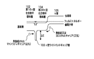
- FIG. 2 is an infrared light emitting element band diagram according to the first embodiment.
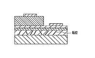
- FIG. 3 is a diagram showing dislocations in the first n-type compound semiconductor layer.
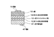
- FIG. 4 is a view showing a modification of the infrared light emitting element according to the first embodiment.
- FIG. 5 is a diagram showing a modification of the infrared light emitting element according to the first embodiment.
- FIG. 6 is a schematic diagram of an infrared light emitting element according to the second embodiment.
- FIG. 7 is a schematic diagram of an infrared light emitting element according to the third embodiment.
- FIG. 8 is an infrared light emitting element band diagram according to the third embodiment.
- FIG. 1 is a schematic diagram of an infrared light emitting device according to the first embodiment.
- FIG. 2 is an infrared light emitting element band diagram according to the first embodiment.
- FIG. 9 is a schematic diagram of an infrared light emitting element according to the fourth embodiment.
- FIG. 10 is a view showing a modification of the infrared light emitting device according to the fourth embodiment.
- FIG. 11 is a schematic diagram of an infrared light emitting device according to the fifth embodiment.
- FIG. 12 is a diagram showing the relationship between the film thickness of the first n-type compound semiconductor layer and the etch pit density.
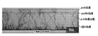
- FIG. 13A is a diagram showing a cross-sectional TEM (transmission electron microscope) observation result of Comparative Example 2-1.
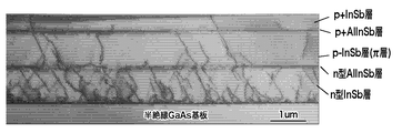
- FIG. 13B is a diagram showing a result of observation by a cross-sectional TEM (transmission electron microscope) of Example 2-1.
- FIG. 13C is a diagram showing a result of observation by a cross-sectional TEM (transmission electron microscope) of Example 2-2.
- FIG. 14 is a diagram showing current-voltage characteristics of PIN diodes using the structures of Comparative Example 2-1 and Example 2-1.
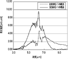
- FIG. 15 is a graph showing the light emission characteristics of PIN diodes using the structures of Comparative Example 2-1 and Example 2-1.
- FIG. 16 is a graph showing the light emission characteristics of PIN diodes using the structures of Example 2-1 and Example 2-2.
- FIG. 1 is a schematic diagram of an infrared light emitting device according to the first embodiment.
- the infrared light emitting element 100 includes a semi-insulating semiconductor substrate 101, a first n-type compound semiconductor layer 102 on the semiconductor substrate 101, and an n-type wide band gap layer on the first n-type compound semiconductor layer 102.
- a p-type doped ⁇ layer 105, an electrode 106 on the ⁇ layer 105, and an electrode 107 on the second n-type compound semiconductor layer 104 are provided.
- the infrared light emitting element 100 is a so-called PN junction diode in which a depletion layer is formed between the second n-type compound semiconductor layer 104 and the ⁇ layer 105. A forward current is passed through the PN junction to recombine carriers to generate infrared rays.
- the band gap of the n-type wide band gap layer 103 is larger than that of the first n-type compound semiconductor layer 102 and the ⁇ layer 105, and the n-type compound semiconductor layer is heated at room temperature. It suppresses the diffusion of holes generated by excitation in the direction of the ⁇ layer, that is, the dark current of the diode.
- FIG. 2 shows such a state. Holes that are minority carriers generated in the first n-type compound semiconductor layer 102 try to diffuse toward the ⁇ layer 105, but have a band gap larger than that of the first n-type compound semiconductor layer 102 and the ⁇ layer 105.
- the dark current is reduced by providing the n-type wide band gap layer 103 that suppresses the diffusion between the first n-type compound semiconductor layer 102 and the ⁇ layer 105.
- the n-type wide band gap layer 103 has its band gap relatively shifted in the valence band direction due to n-type doping, and functions more effectively as a hole diffusion barrier. That is, the n-type wide band gap layer 103 is adjusted so that the band gap and n-type doping suppress the diffusion of holes.
- holes generated by thermal excitation in the ⁇ layer 105 usually move toward the ⁇ layer 105 due to an internal electric field formed by a pn junction, but some of the holes move toward the n-type compound semiconductor layer 102 due to diffusion. And becomes the diffusion current of the diode.
- the intrinsic carrier density is increased due to thermal excitation even at room temperature.
- the diffusion current has a relationship proportional to the square of the intrinsic carrier density, that is, the diffusion current increases as the intrinsic carrier density increases. It is particularly important to suppress large diffusion currents because they reduce the diode resistance of the device.
- the n-type wide band gap layer 103 also serves as a barrier against diffusion current due to holes as shown in FIG. Accordingly, the diffusion current can be suppressed.
- the compound semiconductor layer is a compound semiconductor such as gallium nitride (GaN) or gallium arsenide (GaAs) that has an inherently large band gap and the influence of thermally excited carriers can be ignored, and the diffusion current is originally small. This is an effect obtained because it is a semiconductor having a small band gap as described above.
- the infrared light emitting device 100 when used as a light emitting device as shown in FIG. 2, it is possible to suppress the diffusion of holes injected from the ⁇ layer 105 side into the n-type compound semiconductor layer 102.
- the recombination efficiency of electrons and holes can be improved in the depletion layer formed by the pn junction.
- the necessary energy difference ⁇ E between the n-type wide band gap layer 103 and the valence band is determined by the holes. It needs to be larger than energy.
- the energy given to the holes includes thermal energy, which is about 25 meV at room temperature. Accordingly, the magnitude of ⁇ E in this case is preferably at least thermal energy or more and 25 meV or more at room temperature.
- ⁇ E is preferably larger than at least the potential difference of the PN junction in order to suppress diffusion of holes injected by forward bias into the diode into the n-type compound semiconductor layer 102. . Since the potential difference of the PN junction is usually smaller than the band gap to prevent tunnel leakage current, ⁇ E is at least the energy band gap of the first and second n-type compound semiconductor layers 102 and 104 and the ⁇ layer 105. 50% or more of the size is preferable, more preferably 80% or more, and still more preferably equal or more.
- ⁇ E is preferably 0.09 eV or more at room temperature, more preferably 0.14 eV or more, and still more preferably Is 0.18 eV or more.
- a suitable band gap size of the n-type wide band gap layer 103 is the energy band gap of the first and second n-type compound semiconductor layers 102 and 104 and the ⁇ layer 105. Is preferably 1.5 times or more, more preferably 2 times or more, and still more preferably 2.3 times or more.
- the magnitude of ⁇ E can be adjusted by the electron affinity of the material and the doping concentration of the n-type wide band gap layer in addition to the band gap of the n-type wide band gap layer 103.
- the compound semiconductor constituting the layers other than the n-type wide band gap layer 103 is a narrow band, and in particular, a compound having a band gap of 0.41 eV or less capable of absorbing and generating infrared rays having a wavelength of 3 ⁇ m or longer.
- a semiconductor is preferable. Since the device is assumed to be used at room temperature, the band gap is more preferably 0.41 eV or less at room temperature. However, when the device is not used at room temperature, the band gap is 0 at the use temperature. .41 eV or less is sufficient.
- the effect of suppressing the dark current and the diffusion current of the n-type wide band gap layer 103 increases as the band gap of the compound semiconductor constituting the layers other than the n-type wide band gap layer 103 decreases. Because of that.
- any of InAs, InSb, InAsSb, or InSbN can be used.
- the energy band gaps of InAs and InSb at room temperature are 0.36 eV and 0.18 eV, respectively.
- the band gap of InSb 1-y N y mixed crystal (0 ⁇ y ⁇ 0.01) has a larger nonlinear factor, and the band gap is nearly zero when the composition y of nitrogen N is only 0.01. It has been known.
- any one of AlInSb, GaInSb, AlAs, GaAs, AlSb, GaSb, or a mixed crystal thereof can be used.
- the energy band gap at room temperature of each n-type wide band gap layer is determined by the composition ratio.
- the band gap at room temperature of the Al 0.17 In 0.83 Sb layer is 0.46 eV.
- the above material is more preferable because it is capable of forming a stable compound or mixed crystal semiconductor compared to a material having a high vapor pressure of Hg, such as HgCdTe (MCT), which is difficult to control composition and reproducibility during crystal growth. .
- the ⁇ layer 105 has the same composition as the first n-type compound semiconductor layer 102, and the thickness of the n-type wide band gap layer 103 is set to a critical film. It can be less than or equal to the thickness. The case where the film thickness of the n-type wide band gap layer 103 is below the critical film thickness will be described below.
- the n-type wide band gap layer 103 included in the infrared light emitting element 100 has a band gap larger than that of the first n-type compound semiconductor layer 102 and has a composition different from that of the first n-type compound semiconductor layer 102.
- misfit dislocations generated at the interface between the semiconductor substrate 101 and the first n-type compound semiconductor layer 102 are caused by the n-type wide band gap layer 103. It has been experimentally found that the propagation direction can be changed in the direction parallel to the interface at the interface between the first n-type compound semiconductor layer 102 and the first n-type compound semiconductor layer 102 as shown in FIG. The dislocations whose direction has been changed will cause the dislocations to disappear or form a dislocation loop and return to the interface with the semiconductor substrate 101 again. That is, dislocations can be confined in the first n-type compound semiconductor layer 102. Examples will be described later.
- the effect of reducing the threading dislocation from the substrate interface by the n-type wide band gap layer 103 is that a film having a thickness greater than the critical thickness is grown, and the newly generated dislocations in the film are separated from the substrate interface.
- the n-type wide band gap layer 103 has a larger band gap than the first n-type compound semiconductor layer 102, the second n-type compound semiconductor layer 104, and the ⁇ layer 105, and the composition of the n-type wide band gap layer 103 is the same as that of the first n-type compound semiconductor layer 102. Of different materials. When the composition is different, the lattice constant is generally different, and the n-type wide band gap layer 103 is grown in a lattice-matched manner with the first n-type compound semiconductor layer 102 as a base by distorting the entire lattice.
- the film thickness that allows the n-type wide band gap layer 103 to grow in such a lattice-matched state is the so-called “critical film thickness”.
- critical film thickness is the maximum film thickness at which lattice matching is absorbed by lattice strain without misfit dislocations.
- the thickness of the n-type wide band gap layer 103 is set to be equal to or less than the critical thickness, and the first n-type compound semiconductor layer 102 and the second n-type compound semiconductor layer 104 have the same composition.
- the lattice constants of the n-type compound semiconductor layer 102, the n-type wide band gap layer 103, and the second n-type compound semiconductor layer 104 are the same. For this reason, it is possible to suppress the occurrence of new misfit dislocations from the interface between the n-type wide band gap layer 103, the first n-type compound semiconductor layer 102, and the second n-type compound semiconductor layer 104.
- the n-type wide band gap layer 103 with high crystallinity can be obtained, and the effect of suppressing the above-described dark current and diffusion current can be enhanced. Furthermore, in combination with the effect of reducing the threading dislocation from the interface described above, the crystallinity of the ⁇ layer serving as the active layer can be improved, so that the light emission efficiency can be increased.
- the term “same composition” used in this specification means that defects occur at the interface with the n-type wide band gap layer whose stress due to lattice mismatch is less than the critical film thickness in addition to the case where the composition is completely the same. It is intended to include cases where they are identical to the extent that they are not.
- the semiconductor substrate 101 Si, GaAs or the like can be used.
- the crystal plane has (100), (111), (110) directions, and the like. Since the semi-insulating semiconductor substrate 101 generally has a band gap larger than 0.41 eV and is transparent to long-wavelength infrared rays, it does not hinder the generated infrared rays from the substrate side. Since there is no electrode on the substrate side, infrared rays generated are not blocked by the electrode, which is preferable.
- a semi-insulating substrate is used in this embodiment, an n-type semiconductor substrate may be used as shown in FIG. In this case, one electrode 407 can be formed on the back surface of the substrate as shown in FIG.
- the first n-type compound semiconductor layer 102 is an n-type doped narrow band gap compound semiconductor.
- Narrow band gap compound semiconductors have a much higher electron mobility than holes, and therefore n-type doping can lower the sheet resistance of the semiconductor layer more easily than p-type doping. Therefore, the sheet resistance of the infrared light emitting element 100 can be easily reduced by n-type doping the first n-type compound semiconductor layer 102 occupying a large area in the element structure.
- the series resistance connected in series with the diode on the equivalent circuit of the diode increases.
- the series resistance is preferably as small as possible in order to consume the electric power injected into the element.
- the n-type dopant Si, Te, Sn, S, Se, or the like can be used.
- the n-type doping of the n-type wide band gap layer 103 can be adjusted so as to obtain a desired sheet resistance.
- the n-type doping of the n-type wide band gap layer 103 also has an effect of relatively shifting the band gap in the valence band direction.
- the composition of the n-type wide band gap layer 103 is designed to an appropriate value in consideration of the required band gap size and the ease of thin film growth.
- the composition of Al is 0.06 ⁇ x ⁇ 0.7, more preferably 0.1 ⁇ x ⁇ 0.5, and still more preferably 0.15 ⁇ x ⁇ 0.3.
- the film thickness can be not more than the critical film thickness in each composition, but it is about 10 nm to 30 nm.
- the second n-type compound semiconductor layer 104 is an n-type doped narrow band gap compound semiconductor.
- the n-type doping concentration need not be the same as that of the first n-type compound semiconductor layer 102 or the n-type wide band gap layer 103, but is preferably doped so as not to increase the sheet resistance of the device.
- 1 n-type compound semiconductor layer 102 and n-type wide band gap layer 103 may be the same.
- the ⁇ layer 105 is a p-type doped ⁇ layer.
- the n-type wide band gap layer 103 has a critical film thickness, it has the same composition as the first n-type compound semiconductor layer 102 for the same reason as described for the second n-type compound semiconductor layer 104.
- the doping concentration is preferably less than 1 ⁇ 10 16 atoms / cm 3 or more 1 ⁇ 10 18 atoms / cm 3 in the case of p-type doping, more preferably 1 ⁇ 10 16 atoms / cm 3 or more 1 ⁇ 10 17 atoms / cm 3 Is less than.
- the film thickness of the ⁇ layer 105 is preferably 0.1 ⁇ m or more and 3 ⁇ m or less, more preferably 0.5 ⁇ m or more and 2 ⁇ m or less.
- the p-type dopant Be, Zn, Cd, C, Mg, Ge, Cr, or the like can be used.
- Each compound semiconductor layer constituting the infrared light emitting device 100 according to the present embodiment can be formed using various film forming methods. For example, molecular beam epitaxy (MBE) method, metal organic vapor phase epitaxy (MOVPE) method, etc. are preferable.
- MBE molecular beam epitaxy
- MOVPE metal organic vapor phase epitaxy
- a processing method of the element for example, first, a step is formed for making contact with the n-type doping layer using acid or ion milling, then, mesa etching for element isolation is performed, and then SiN or After covering with a passivation film such as SiO 2 , only the electrode part is opened, and an electrode such as Ti / Au or Cr / Au is formed by a lift-off method or the like.
- a structure in which a plurality of elements are connected in series can be manufactured by using a dedicated mask set.
- the second n-type compound semiconductor layer 104 has the same composition as the first n-type compound semiconductor layer 102 at the interface with the n-type wide band gap layer 103, and the composition is inclined in the film thickness direction. Can be used.
- the composition of the ⁇ layer 105 is made to have a critical thickness. In this case, the infrared emission wavelength can be adjusted.
- the ⁇ layer 105 may be disposed directly on the n-type wide band gap layer 103.
- the p-type doping composition transition layer having the same composition as that of the first n-type compound semiconductor layer 102 at the interface and the composition being inclined in the film thickness direction is formed between the n-type wide band gap layer 103 and the ⁇ layer 105. It may be provided between them.
- the interface capable of stopping dislocations can be increased to a plurality, and the effect of suppressing propagation of dislocations to the PN junction portion can be further enhanced.
- the film thickness of the n-type wide band gap layer is all equal to or less than the critical film thickness, and the film thickness of the n-type compound semiconductor layer therebetween is an n-type doped layer (hereinafter referred to as “n-type doping layer”). .) It can be arbitrarily determined in consideration of the entire film thickness. Further, how many layers are repeatedly laminated can be arbitrarily determined in consideration of the film thickness of the entire n-type doping layer.
- the semiconductor substrate 101 is transparent to the infrared rays, and the n-type wide band gap layer 103 is also transparent because of the size of the band gap. Infrared rays generated in the depletion layer portion of the PN junction can be taken out efficiently, and the external quantum efficiency of the device can be improved.
- the doping concentration is preferably 1 ⁇ 10 18 atoms / cm 3 or more, more preferably 1 ⁇ 10 19 atoms / cm 3 or more.
- a lattice constant is present between the semiconductor substrate 101 and the first n-type compound semiconductor layer 102.
- a buffer layer that is approximately between the first n-type compound semiconductor layer 102 and the lattice mismatch is relaxed.
- a material that does not absorb infrared light is selected for the buffer layer.
- a p-type is used for the ⁇ layer 105 and an n-type layer is used in addition to the ⁇ layer 105.
- the electron dark current and diffusion current are The effect of suppressing the deterioration of the device characteristics due to suppression and crystal defects.
- the sheet resistance of the element increases when p-type doping is used.
- p-type compound semiconductors easily absorb long-wavelength infrared rays, it is difficult to extract infrared rays from the substrate side.
- the electrode 107 is provided on the second n-type compound semiconductor layer 104, but it is connected to the n-type wide band gap layer 103 or the first n-type compound semiconductor layer 102. You may provide in the form to do. However, in order to reduce the sheet resistance of the n-type doping layer, it is better that the film thickness thereof is thick. Therefore, the position where the electrode 107 is provided is just above the second n-type compound semiconductor layer (or n) as shown in FIG. The upper surface of the type doping layer) is preferred.
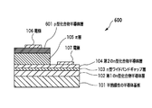
- FIG. 6 shows an infrared light emitting device 600 according to the second embodiment.
- the semiconductor substrate 101 to the ⁇ layer 105 are the same as those in the first embodiment, and similar modifications can be considered.
- the infrared light emitting device 600 is disposed on the ⁇ layer 105, is p-type doped at a higher concentration than the ⁇ layer 105, and has the same composition as the first n-type compound semiconductor layer or the ⁇ layer.
- a layer 601 is further provided. This structure is a so-called PIN diode structure.
- the p-type doping concentration of the p-type compound semiconductor layer 601 is preferably 7 ⁇ 10 17 atoms / cm 3 or more, more preferably 1 ⁇ 10 18 atoms / cm 3 or more.
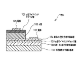
- FIG. 7 shows an infrared light emitting device 700 according to the third embodiment.
- the semiconductor substrate 101 to the ⁇ layer 105 are the same as those in the first embodiment, and similar modifications can be considered.
- Infrared light emitting device 700 is disposed directly on ⁇ layer 105, is p-type doped at a higher concentration than ⁇ layer 105, and has a larger band gap than first n-type compound semiconductor layer 102 and ⁇ layer 105.
- a p-type wide band gap layer 701 is further provided. This structure is also a so-called PIN diode structure.
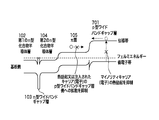
- FIG. 8 is a schematic diagram of an energy band gap in the infrared light emitting device according to the third embodiment.
- the p-type wide band gap layer 701 is thermally excited by electrons that are minority carriers.
- production can be suppressed effectively. This suppresses dark current due to electrons flowing from the p-type wide band gap layer 701 to the ⁇ layer 105 side, and also causes diffusion of electrons generated by thermal excitation in the ⁇ layer 105 and flowing to the p-type wide band gap layer 701 side. It is possible to effectively suppress the diode resistance from decreasing.
- the p-type wide band gap layer 701 has a wide band gap that cannot generate infrared rays in a long wavelength band.
- the generation of infrared rays is performed in the ⁇ layer 105, there is no problem.
- the ⁇ layer In 105 since electrons injected from the n-type doping layer (101 to 104) side can be further suppressed from diffusing into the p-type wide band gap layer 701 than in the second embodiment, the ⁇ layer In 105, the recombination emission efficiency of electrons and holes can be further improved.
- the composition of the p-type wide band gap layer 701 is designed to an appropriate value in consideration of the required band gap size and the ease of thin film growth.
- the composition of Al is 0.06 ⁇ x ⁇ 0.7, more preferably 0.8. 1 ⁇ x ⁇ 0.5, more preferably 0.15 ⁇ x ⁇ 0.3.
- the p-type doping concentration of the p-type wide band gap layer 701 is preferably 7 ⁇ 10 17 atoms / cm 3 or more, more preferably 1 ⁇ 10 18 atoms / cm 3 or more.
- FIG. 9 shows an infrared light emitting device 900 according to the fourth embodiment.
- the semiconductor substrate 101 to the ⁇ layer 105 are the same as those in the first embodiment, and similar modifications can be considered.
- the p-type wide band gap layer which is p-type doped at a higher concentration than the ⁇ layer 105 on the ⁇ layer 105 and has a larger band gap than the first n-type compound semiconductor layer 102 and the ⁇ layer 105 is that Although common to the third embodiment, in this embodiment, the p-type wide band gap layer 901 is set to a critical film thickness or less (approximately 10 nm to 30 nm).
- a p-type compound semiconductor protective layer 902 that is p-type doped at a higher concentration than the ⁇ layer 105 is provided on the p-type wide band gap layer 901.
- the p-type wide band gap layer 901 is very thin with a critical film thickness or less. Therefore, if an electrode is directly formed on the p-type wide band gap layer 901, there is a possibility of some damage during the electrode formation process.
- the p-type compound semiconductor protective layer 902 has a ratio that protects the p-type wide band gap layer 901 from such damage.
- the p-type compound semiconductor protective layer 902 serves as a contact layer with the electrode 106.
- the contact resistance with the electrode becomes a series resistance on the equivalent circuit and consumes the power of the light emitting element. Therefore, in order to reduce the contact resistance between the p-type compound semiconductor protective layer 902 and the electrode 106, the p-type compound semiconductor protective layer 902 is doped with p-type doping equal to or more than the p-type wide band gap layer 901. Is preferred.
- the p-type doping concentration is preferably 7 ⁇ 10 17 atoms / cm 3 or more, more preferably 1 ⁇ 10 18 atoms / cm 3 or more.
- the thickness of the p-type compound semiconductor protective layer 902 is preferably 0.05 ⁇ m or more and 1 ⁇ m or less, more preferably 0.1 ⁇ m or more and 0.7 ⁇ m or less.
- the film sheet resistance is preferably as small as possible. Therefore, the band gap of the p-type compound semiconductor protective layer 902 is preferably smaller than that of the p-type wide band gap layer 801. This is because a semiconductor with a small band gap has a small film sheet resistance.
- the composition of the p-type compound semiconductor protective layer 902 is the same as that of the first n-type compound semiconductor layer 102 or the ⁇ layer 105, the film sheet resistance can be reduced because the band gap is small.
- the lattice constant is close to the p-type wide band gap layer 901 having a critical thickness or less, no stress is applied to the p-type wide band gap layer 901, and the crystallinity can be further improved.
- the lattice constants of the ⁇ layer 105, the p-type wide band gap layer 901, and the p-type compound semiconductor protective layer 902 match, a highly crystalline film can be grown. preferable.
- FIG. 10 shows a modification 110 of the infrared light emitting device 900.
- the infrared light emitting device 110 has a structure in which the ⁇ layer 105 is directly disposed on the n-type wide band gap layer 103 as described in the first embodiment.
- the ⁇ layer 105 that is a light emitting layer is sandwiched between the n-type wide band gap layer 103 and the p type wide band gap layer 901, and the carrier is effective in the ⁇ layer 105.
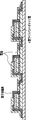
- FIG. 11 shows a structure in which a plurality of infrared light emitting elements are provided on a semiconductor substrate. Each infrared light emitting element is connected in series by an electrode.
- an insulating protective film is laminated on the whole, and a window is opened in a contact portion with the element, and then the electrodes are connected in series. Can be obtained by forming.
- the substrate is a conductive substrate such as an InSb substrate.
- the first n-type compound semiconductor layer that grows first on the semiconductor substrate is hetero-growth having a large lattice mismatch with the substrate material. Therefore, the first n-type compound semiconductor layer grows in an island shape first, and the grown islands are in contact with each other and bonded together. In this way, the growth process becomes a continuous film. Therefore, when the film thickness is very thin, a continuous film cannot be formed, or sufficient crystallinity may not be obtained even with a continuous film. Even if an n-type wide band gap layer is grown on such a crystalline first n-type compound semiconductor layer, the crystallinity of the lower first n-type compound semiconductor layer is affected and the n-type wide band gap is affected. The layer also cannot obtain sufficient crystallinity and cannot exhibit a sufficient crystal defect propagation suppressing effect.
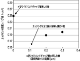
- an InSb film having a total thickness of 1 ⁇ m is grown on a GaAs substrate, an n-type wide band gap layer Al 0.17 In 0.83 Sb having a thickness of 20 nm is positioned at 0.1 ⁇ m, 0.2 ⁇ m, and 0.3 ⁇ m from the substrate. Inserted into each.
- dislocations reaching the surface so-called threading dislocations, are obtained as etch pits. It was. By counting the number of etch pits, the number of dislocations reaching the surface of the film can be obtained.
- FIG. 12 is a graph showing the relationship between the number of etch pits thus obtained and the insertion position of the n-type wide band gap layer Al 0.17 In 0.83 Sb.
- the insertion position of the n-type wide band gap layer Al 0.17 In 0.83 Sb is 0.2 ⁇ m and 0.3 ⁇ m from the substrate, compared with the film without the n-type wide band gap layer Al 0.17 In 0.83 Sb.
- the number of threading dislocations is reduced by 20% or more. That is, the n-type wide band gap layer Al 0.17 In 0.83 Sb effectively suppresses the propagation of crystal defects.
- the insertion position of the n-type wide band gap layer is preferably a position away from the substrate by 0.1 ⁇ m.
- the film thickness of the first n-type compound semiconductor layer is preferably more than 0.1 ⁇ m.
- the preferable film thickness of the first n-type compound semiconductor layer is 0.1 ⁇ m ⁇ x ⁇ 3.0 ⁇ m, more preferably 0.2 ⁇ m ⁇ x ⁇ 2.0 ⁇ m, and still more preferably 0.3 ⁇ m ⁇ x ⁇ 1.0 ⁇ m.
- the total thickness of the n-type compound semiconductor layer including the first and second n-type compound semiconductor layers may be thicker than 0.1 ⁇ m, preferably thicker than 0.1 ⁇ m and 3 ⁇ m or less, more preferably It is 0.7 ⁇ m or more and 2 ⁇ m or less.
- Example 2-1 The element structure shown in FIG. 10 was fabricated by the MBE method. First, an InSb layer (first n-type compound semiconductor layer) doped with 1.0 ⁇ 10 19 atoms / cm 3 of Sn (n-type dopant) is formed on a semi-insulating GaAs single crystal substrate (001). An Al 0.17 In 0.83 Sb layer (n-type wide bandgap layer), which is also doped with Sn (n-type dopant) at 1.0 ⁇ 10 19 atoms / cm 3 , is grown on this layer by 0.02 ⁇ m.
- InSb layer first n-type compound semiconductor layer
- Sn n-type dopant
- the band gap at room temperature of each InSb layer is 0.18 eV
- the band gap at room temperature of each Al 0.17 In 0.83 Sb layer is 0.46 eV. The same applies to other examples and comparative examples.
- the cross-sectional TEM (transmission electron microscope) observation was performed about the infrared light emitting element produced in this way. First, it was sliced by an ion milling method, and then observed under an acceleration voltage of 300 kV using an electron microscope of HITACHI H-9000NAR.
- FIG. 13B shows an observation result at a magnification of 12500 times.
- the diagonal lines seen in the figure are dislocations. As can be seen from the photograph, dislocations generated from the interface with the substrate are bent by the n-type Al 0.17 In 0.83 Sb layer (n-type wide band gap layer) between the n-type InSb layer and the ⁇ layer, It can be clearly seen that the dislocation propagation to the ⁇ layer is greatly suppressed.
- the 0.02 ⁇ m thick Al 0.17 In 0.83 Sb layer is less than the critical thickness with respect to the InSb base, and the InSb layer and the Al 0.17 In 0.83 Sb layer are completely lattice-matched in the direction parallel to the film surface. This was confirmed from the photograph of the cross-sectional TEM and the result of reciprocal lattice mapping of the (115) plane by X-ray diffraction.
- Comparative Example 2-1 A structure was prepared by removing the Al 0.17 In 0.83 Sb layer (n-type wide band gap layer) from Example 2-1.
- FIG. 13A shows the result of cross-sectional TEM observation of this element under the same conditions as in Example 2-1. As can be seen from FIG. 13A, dislocations generated at the interface penetrate the ⁇ layer.
- Example 2-2 In the element structure shown in FIG. 10, a structure in which five n-type wide band gap layers were inserted in the first n-type compound semiconductor layer as shown in FIG. 5 was fabricated by the MBE method.
- an InSb layer doped with 1.0 ⁇ 10 19 atoms / cm 3 of Sn (n-type dopant) is grown to 0.5 ⁇ m on a semi-insulating GaAs single crystal substrate (001) surface.
- An Al 0.17 In 0.83 Sb layer (n-type wide band gap layer) doped with 1.0 ⁇ 10 19 atoms / cm 3 of Sn (n-type dopant) is grown to 0.02 ⁇ m, and Sn (n-type dopant) is grown thereon.
- An InSb layer doped with 1.0 ⁇ 10 19 atoms / cm 3 is grown by 0.02 ⁇ m. Thereafter, the same 0.02 ⁇ m Al 0.17 In 0.83 Sb layer (n-type wide bandgap layer) and 0.02 ⁇ m InSb layer as above are alternately stacked, and the Al 0.17 In 0.83 Sb layer (n-type wide bandgap layer). ) Repeatedly until a total of 5 layers are obtained. On the fifth Al 0.17 In 0.83 Sb layer (n-type wide band gap layer), an InSb layer doped with 1.0 ⁇ 10 19 atoms / cm 3 of Sn (n-type dopant) is grown by 0.3 ⁇ m.
- Sb layer doped with 1.0 ⁇ 10 19 atoms / cm 3 of Sn (n-type dopant) is further grown thereon by 0.02 ⁇ m.
- the n-type doping layer (Sn doping layer) so far has a total thickness of 1 ⁇ m.
- An InSb layer ( ⁇ layer) doped with 6.0 ⁇ 10 16 atoms / cm 3 of Zn (p-type dopant) is grown on this layer by 1.0 ⁇ m, and Zn (p-type dopant) is grown on this layer at 2.0 ⁇ 10.
- FIG. 13C shows the result of cross-sectional TEM observation of the infrared light emitting device thus fabricated under the same conditions as in Example 2-1.
- the dislocation generated at the interface is further effectively suppressed by the five inserted Al 0.17 In 0.83 Sb layers.
- Example 2-3 Using the structure of Example 2-1, a PIN diode was fabricated by the following procedure. First, step formation etching for making contact with the n-type doping layer was performed with an acid, and then mesa etching for element isolation was performed on the compound semiconductor thin film on which the step was formed. Thereafter, the entire surface (GaAs substrate and compound semiconductor structure formed on the substrate) was covered with a SiN protective film by using plasma CVD. Next, a window was opened only on the electrode portion on the formed SiN protective film, Au / Ti (Ti was the film side) was EB evaporated, and an electrode was formed by a lift-off method. The PN junction portion has an octagonal shape, and the area is designed to be 120.7 ⁇ m 2 . A PIN diode was also manufactured using the structure of Comparative Example 2-1.
- FIG. 14 shows the current-voltage characteristics of the PIN diode fabricated as described above.
- the current at the time of reverse bias that is, the dark current of the diode
- the current rising at the time of the positive bias is shifted to the larger bias side. This is an effect of suppressing the diffusion current of the diode.
- Example 2-4 Using the structure of Example 2-1, a PIN diode was fabricated in the same procedure as in Example 2-3. However, the PN junction portion was designed to be a circle having a diameter of 500 ⁇ m. This is a very large element compared to Example 2-3.
- the light emission characteristics of the PIN diode thus fabricated were evaluated by the following procedure. First, a PIN diode was attached on a glass epoxy substrate having a hole for extracting light, and the electrode and a terminal on the glass epoxy substrate were connected by wire bonding. A pulse generator having a frequency of 1 kHz, a duty cycle (Duty Cycle) of 50%, and a current value of 100 mA (peak to peak value) was applied to the device from this terminal using a pulse generator to drive the device as a light emitting device. . The measurement of the luminescent property was performed by measuring the infrared light taken out from the hole of the glass epoxy substrate by FTIR (Fourier transform infrared spectrophotometer).
- FTIR Fastier transform infrared spectrophotometer
- the FTIR used is Nexus 870 FTIR manufactured by Nicolet. The measurement is performed at room temperature (25 ° C.), and the element is not cooled during the measurement. Further, a similar PIN diode structure was fabricated using the structure of Comparative Example 2-1, and the light emission characteristics were measured.
- FIG. 15 shows the result of normalization by dividing the infrared emission intensity obtained by measurement by the value of bias voltage ⁇ bias current (100 mA) with respect to each spectral wavelength.
- the PIN diode using the structure of Example 2-1 compared with the PIN diode using the structure of Comparative Example 2-1 that does not have an n-type wide bandgap layer has a light emission intensity at a wavelength of 6.3 ⁇ m that exhibits a peak. It was confirmed that the strength was significantly increased to about 2.3 times.
- Example 2-5 Using the structure of Example 2-2, a PIN diode structure similar to that of Example 2-4 was fabricated, and the light emission characteristics were measured.
- FIG. 16 shows the light emission intensity in the wavelength range of 5 ⁇ m to 6 ⁇ m of the PIN diode of Example 2-4 and the PIN diode of this example using the structure of Example 2-1. This wavelength range is the range where the difference is most clearly obtained between the two PIN diodes. In the PIN diode of this example, a light emission intensity stronger than that of Example 2-4 was obtained.
Landscapes
- Led Devices (AREA)
Abstract
Priority Applications (4)
| Application Number | Priority Date | Filing Date | Title |
|---|---|---|---|
| EP09719506.9A EP2254165A4 (fr) | 2008-03-14 | 2009-03-13 | Dispositif emettant une lumiere infrarouge |
| JP2010502910A JP5526360B2 (ja) | 2008-03-14 | 2009-03-13 | 赤外線発光素子 |
| CN2009801086609A CN101971367B (zh) | 2008-03-14 | 2009-03-13 | 红外线发光元件 |
| US12/921,318 US8309980B2 (en) | 2008-03-14 | 2009-03-13 | Infrared light emitting device |
Applications Claiming Priority (2)
| Application Number | Priority Date | Filing Date | Title |
|---|---|---|---|
| JP2008066404 | 2008-03-14 | ||
| JP2008-066404 | 2008-03-14 |
Publications (1)
| Publication Number | Publication Date |
|---|---|
| WO2009113685A1 true WO2009113685A1 (fr) | 2009-09-17 |
Family
ID=41065342
Family Applications (1)
| Application Number | Title | Priority Date | Filing Date |
|---|---|---|---|
| PCT/JP2009/054954 Ceased WO2009113685A1 (fr) | 2008-03-14 | 2009-03-13 | Dispositif émettant une lumière infrarouge |
Country Status (6)
| Country | Link |
|---|---|
| US (1) | US8309980B2 (fr) |
| EP (1) | EP2254165A4 (fr) |
| JP (2) | JP5526360B2 (fr) |
| CN (1) | CN101971367B (fr) |
| TW (1) | TWI427824B (fr) |
| WO (1) | WO2009113685A1 (fr) |
Cited By (10)
| Publication number | Priority date | Publication date | Assignee | Title |
|---|---|---|---|---|
| JP2015133386A (ja) * | 2014-01-10 | 2015-07-23 | 旭化成エレクトロニクス株式会社 | 発光素子 |
| JP2016149392A (ja) * | 2015-02-10 | 2016-08-18 | 旭化成エレクトロニクス株式会社 | 赤外線発光ダイオード |
| JP2016152259A (ja) * | 2015-02-16 | 2016-08-22 | 旭化成エレクトロニクス株式会社 | 赤外線発光素子及び赤外線発光素子の製造方法 |
| JP2016163009A (ja) * | 2015-03-05 | 2016-09-05 | 旭化成エレクトロニクス株式会社 | 赤外線発光素子 |
| JP2018067632A (ja) * | 2016-10-19 | 2018-04-26 | 旭化成エレクトロニクス株式会社 | 赤外線発光素子 |
| JP2019009438A (ja) * | 2017-06-20 | 2019-01-17 | 旭化成エレクトロニクス株式会社 | 赤外線発光ダイオード |
| JP2019114772A (ja) * | 2017-12-21 | 2019-07-11 | 旭化成エレクトロニクス株式会社 | 赤外線発光素子 |
| JP2020126977A (ja) * | 2019-02-06 | 2020-08-20 | 旭化成エレクトロニクス株式会社 | 赤外線発光素子 |
| JP2022031353A (ja) * | 2017-12-21 | 2022-02-18 | 旭化成エレクトロニクス株式会社 | 赤外線発光素子 |
| US11935973B2 (en) | 2018-02-28 | 2024-03-19 | Asahi Kasei Microdevices Corporation | Infrared detecting device |
Families Citing this family (4)
| Publication number | Priority date | Publication date | Assignee | Title |
|---|---|---|---|---|
| US8471329B2 (en) * | 2011-11-16 | 2013-06-25 | Taiwan Semiconductor Manufacturing Company, Ltd. | Tunnel FET and methods for forming the same |
| JP6132746B2 (ja) * | 2013-11-05 | 2017-05-24 | 浜松ホトニクス株式会社 | 赤外線検出素子 |
| KR102356696B1 (ko) * | 2015-07-03 | 2022-01-26 | 삼성전자주식회사 | 유기 광전 소자 및 이미지 센서 |
| CN108258096B (zh) * | 2016-12-28 | 2021-03-02 | 英属开曼群岛商錼创科技股份有限公司 | 发光二极体晶片 |
Citations (9)
| Publication number | Priority date | Publication date | Assignee | Title |
|---|---|---|---|---|
| JPS62291985A (ja) * | 1986-06-12 | 1987-12-18 | Kokusai Denshin Denwa Co Ltd <Kdd> | 半導体レ−ザ |
| JPS649668A (en) * | 1987-07-02 | 1989-01-12 | Kokusai Denshin Denwa Co Ltd | Infrared ray emitting element |
| JPH01264287A (ja) * | 1988-04-14 | 1989-10-20 | Fujitsu Ltd | 半導体発光装置 |
| JPH0653602A (ja) * | 1992-07-31 | 1994-02-25 | Hitachi Ltd | 半導体レーザ素子 |
| JPH08250810A (ja) * | 1995-03-08 | 1996-09-27 | Sharp Corp | ミニバンドを有する半導体素子 |
| JPH10163567A (ja) * | 1996-12-02 | 1998-06-19 | Nec Corp | 多重量子井戸型半導体レーザ |
| JP2000501238A (ja) * | 1995-11-29 | 2000-02-02 | イギリス国 | 低抵抗接点半導体ダイオード |
| JP2001284737A (ja) * | 2000-03-31 | 2001-10-12 | Ricoh Co Ltd | レーザ半導体装置 |
| JP2004031635A (ja) * | 2002-06-26 | 2004-01-29 | Sumitomo Electric Ind Ltd | 白色発光led |
Family Cites Families (9)
| Publication number | Priority date | Publication date | Assignee | Title |
|---|---|---|---|---|
| JPS63306687A (ja) * | 1987-06-08 | 1988-12-14 | Fujitsu Ltd | 半導体発光装置の製造方法 |
| JPH0653615A (ja) * | 1992-08-03 | 1994-02-25 | Seiko Epson Corp | 光センシング装置および光センシング装置用半導体レーザ |
| JP2699805B2 (ja) * | 1993-05-14 | 1998-01-19 | 日本電気株式会社 | 光検出器および光発信器 |
| JPH0779047A (ja) * | 1993-09-08 | 1995-03-20 | Nippon Telegr & Teleph Corp <Ntt> | 赤外半導体発光素子 |
| GB9814462D0 (en) * | 1998-07-04 | 1998-09-02 | Secr Defence | Infrared light emitting diodes |
| JP2002125982A (ja) * | 2000-10-24 | 2002-05-08 | Mitsunobu Miyagi | レーザー医療装置 |
| JP4148764B2 (ja) * | 2002-12-03 | 2008-09-10 | 株式会社沖データ | 半導体発光装置用半導体エピタキシャル構造および半導体発光装置 |
| JP2004361502A (ja) * | 2003-06-02 | 2004-12-24 | Sumitomo Electric Ind Ltd | 光送受信モジュール |
| TWI261934B (en) * | 2003-09-09 | 2006-09-11 | Asahi Kasei Emd Corp | Infrared sensing IC, infrared sensor and method for producing the same |
-
2009
- 2009-03-11 TW TW098107813A patent/TWI427824B/zh not_active IP Right Cessation
- 2009-03-13 WO PCT/JP2009/054954 patent/WO2009113685A1/fr not_active Ceased
- 2009-03-13 EP EP09719506.9A patent/EP2254165A4/fr not_active Withdrawn
- 2009-03-13 US US12/921,318 patent/US8309980B2/en active Active
- 2009-03-13 CN CN2009801086609A patent/CN101971367B/zh not_active Expired - Fee Related
- 2009-03-13 JP JP2010502910A patent/JP5526360B2/ja active Active
-
2013
- 2013-10-21 JP JP2013218585A patent/JP2014013944A/ja active Pending
Patent Citations (9)
| Publication number | Priority date | Publication date | Assignee | Title |
|---|---|---|---|---|
| JPS62291985A (ja) * | 1986-06-12 | 1987-12-18 | Kokusai Denshin Denwa Co Ltd <Kdd> | 半導体レ−ザ |
| JPS649668A (en) * | 1987-07-02 | 1989-01-12 | Kokusai Denshin Denwa Co Ltd | Infrared ray emitting element |
| JPH01264287A (ja) * | 1988-04-14 | 1989-10-20 | Fujitsu Ltd | 半導体発光装置 |
| JPH0653602A (ja) * | 1992-07-31 | 1994-02-25 | Hitachi Ltd | 半導体レーザ素子 |
| JPH08250810A (ja) * | 1995-03-08 | 1996-09-27 | Sharp Corp | ミニバンドを有する半導体素子 |
| JP2000501238A (ja) * | 1995-11-29 | 2000-02-02 | イギリス国 | 低抵抗接点半導体ダイオード |
| JPH10163567A (ja) * | 1996-12-02 | 1998-06-19 | Nec Corp | 多重量子井戸型半導体レーザ |
| JP2001284737A (ja) * | 2000-03-31 | 2001-10-12 | Ricoh Co Ltd | レーザ半導体装置 |
| JP2004031635A (ja) * | 2002-06-26 | 2004-01-29 | Sumitomo Electric Ind Ltd | 白色発光led |
Non-Patent Citations (2)
| Title |
|---|
| See also references of EP2254165A4 |
| T. ASHLEY ET AL.: "Uncooled InSb/Inl-XAlXSb mid-infrared emitter", APPLIED PHYSICS LETTERS, vol. 64, no. 18, 2 May 1994 (1994-05-02), pages 2433 - 2435 |
Cited By (15)
| Publication number | Priority date | Publication date | Assignee | Title |
|---|---|---|---|---|
| JP2015133386A (ja) * | 2014-01-10 | 2015-07-23 | 旭化成エレクトロニクス株式会社 | 発光素子 |
| JP2016149392A (ja) * | 2015-02-10 | 2016-08-18 | 旭化成エレクトロニクス株式会社 | 赤外線発光ダイオード |
| JP2016152259A (ja) * | 2015-02-16 | 2016-08-22 | 旭化成エレクトロニクス株式会社 | 赤外線発光素子及び赤外線発光素子の製造方法 |
| JP2016163009A (ja) * | 2015-03-05 | 2016-09-05 | 旭化成エレクトロニクス株式会社 | 赤外線発光素子 |
| JP2018067632A (ja) * | 2016-10-19 | 2018-04-26 | 旭化成エレクトロニクス株式会社 | 赤外線発光素子 |
| JP7233859B2 (ja) | 2017-06-20 | 2023-03-07 | 旭化成エレクトロニクス株式会社 | 赤外線発光ダイオード |
| JP2019009438A (ja) * | 2017-06-20 | 2019-01-17 | 旭化成エレクトロニクス株式会社 | 赤外線発光ダイオード |
| JP2019114772A (ja) * | 2017-12-21 | 2019-07-11 | 旭化成エレクトロニクス株式会社 | 赤外線発光素子 |
| JP2022031353A (ja) * | 2017-12-21 | 2022-02-18 | 旭化成エレクトロニクス株式会社 | 赤外線発光素子 |
| JP7554176B2 (ja) | 2017-12-21 | 2024-09-19 | 旭化成エレクトロニクス株式会社 | 赤外線発光素子 |
| US11935973B2 (en) | 2018-02-28 | 2024-03-19 | Asahi Kasei Microdevices Corporation | Infrared detecting device |
| US12408473B2 (en) | 2018-02-28 | 2025-09-02 | Asahi Kasei Microdevices Corporation | Infrared detecting device |
| US10797198B2 (en) | 2019-02-06 | 2020-10-06 | Asahi Kasei Microdevices Corporation | Infrared light emitting device having light emitting layer containing Al, In, and Sb |
| JP7060530B2 (ja) | 2019-02-06 | 2022-04-26 | 旭化成エレクトロニクス株式会社 | 赤外線発光素子 |
| JP2020126977A (ja) * | 2019-02-06 | 2020-08-20 | 旭化成エレクトロニクス株式会社 | 赤外線発光素子 |
Also Published As
| Publication number | Publication date |
|---|---|
| TWI427824B (zh) | 2014-02-21 |
| EP2254165A1 (fr) | 2010-11-24 |
| JP2014013944A (ja) | 2014-01-23 |
| US8309980B2 (en) | 2012-11-13 |
| CN101971367B (zh) | 2012-09-26 |
| JPWO2009113685A1 (ja) | 2011-07-21 |
| JP5526360B2 (ja) | 2014-06-18 |
| EP2254165A4 (fr) | 2014-12-24 |
| CN101971367A (zh) | 2011-02-09 |
| US20110018010A1 (en) | 2011-01-27 |
| TW201003992A (en) | 2010-01-16 |
Similar Documents
| Publication | Publication Date | Title |
|---|---|---|
| JP5526360B2 (ja) | 赤外線発光素子 | |
| JP5266521B2 (ja) | 赤外線センサ、及び赤外線センサic | |
| Xie et al. | Ultra-low dark current AlGaN-based solar-blind metal–semiconductor–metal photodetectors for high-temperature applications | |
| Zhang et al. | Photovoltaic effects in GaN structures with p‐n junctions | |
| Xu et al. | Graphene GaN-based Schottky ultraviolet detectors | |
| US20070126021A1 (en) | Metal oxide semiconductor film structures and methods | |
| JP5528882B2 (ja) | 赤外線センサ | |
| CN108305911B (zh) | 吸收、倍增层分离结构的ⅲ族氮化物半导体雪崩光电探测器 | |
| US8450771B2 (en) | Semiconductor device and fabrication method | |
| JP6283324B2 (ja) | 赤外線発光素子 | |
| Vonsovici et al. | Room temperature photocurrent spectroscopy of SiGe/Si pin photodiodes grown by selective epitaxy | |
| JP5063929B2 (ja) | 赤外線センサ | |
| JP2015088602A (ja) | 半導体光デバイス | |
| US20120073658A1 (en) | Solar Cell and Method for Fabricating the Same | |
| Razeghi et al. | AlGaN ultraviolet detectors | |
| Das | Enhanced performance of LWIR LED devices by backside thinning and isolating the pixels | |
| Głuch et al. | Integrated PbTe Quantum Dots for Two-Color Detection in II–VI Wide-Bandgap Diodes | |
| Lee | Reduction of leakage current of large-area high-resistivity silicon pin photodiodes for detection at 1.06 µm | |
| JP2023143360A (ja) | 赤外線センサ | |
| CN116314398A (zh) | 一种平面结构超晶格红外探测器 | |
| CN120475784A (zh) | 一种背照射吸收层调控掺杂紫外探测器 | |
| Sablon et al. | Quantum dot solar cells: Effective conversion of IR radiation due to inter-dot n-doping | |
| JPH06302840A (ja) | 太陽電池 | |
| Leea et al. | MH Liaoa, C.-Y. Yua, C.-F. Huanga, C.-H. Lina, C.-J. Leea, M.-H. Yua, ST Changb, C.-Y. Lianga | |
| Ruhle et al. | A (Ga, Al) as Semiconductor Scintillator with Monolithically Integrated Photodiode: A New Detector |
Legal Events
| Date | Code | Title | Description |
|---|---|---|---|
| WWE | Wipo information: entry into national phase |
Ref document number: 200980108660.9 Country of ref document: CN |
|
| 121 | Ep: the epo has been informed by wipo that ep was designated in this application |
Ref document number: 09719506 Country of ref document: EP Kind code of ref document: A1 |
|
| WWE | Wipo information: entry into national phase |
Ref document number: 2010502910 Country of ref document: JP |
|
| WWE | Wipo information: entry into national phase |
Ref document number: 12921318 Country of ref document: US Ref document number: 2009719506 Country of ref document: EP |
|
| NENP | Non-entry into the national phase |
Ref country code: DE |