WO2009128179A1 - Substrat de matrice tft et dispositif d'affichage à cristaux liquides - Google Patents
Substrat de matrice tft et dispositif d'affichage à cristaux liquides Download PDFInfo
- Publication number
- WO2009128179A1 WO2009128179A1 PCT/JP2008/071843 JP2008071843W WO2009128179A1 WO 2009128179 A1 WO2009128179 A1 WO 2009128179A1 JP 2008071843 W JP2008071843 W JP 2008071843W WO 2009128179 A1 WO2009128179 A1 WO 2009128179A1
- Authority
- WO
- WIPO (PCT)
- Prior art keywords
- metal
- tft array
- array substrate
- drive circuit
- tft
- Prior art date
- Legal status (The legal status is an assumption and is not a legal conclusion. Google has not performed a legal analysis and makes no representation as to the accuracy of the status listed.)
- Ceased
Links
Images



Classifications
-
- G—PHYSICS
- G02—OPTICS
- G02F—OPTICAL DEVICES OR ARRANGEMENTS FOR THE CONTROL OF LIGHT BY MODIFICATION OF THE OPTICAL PROPERTIES OF THE MEDIA OF THE ELEMENTS INVOLVED THEREIN; NON-LINEAR OPTICS; FREQUENCY-CHANGING OF LIGHT; OPTICAL LOGIC ELEMENTS; OPTICAL ANALOGUE/DIGITAL CONVERTERS
- G02F1/00—Devices or arrangements for the control of the intensity, colour, phase, polarisation or direction of light arriving from an independent light source, e.g. switching, gating or modulating; Non-linear optics
- G02F1/01—Devices or arrangements for the control of the intensity, colour, phase, polarisation or direction of light arriving from an independent light source, e.g. switching, gating or modulating; Non-linear optics for the control of the intensity, phase, polarisation or colour
- G02F1/13—Devices or arrangements for the control of the intensity, colour, phase, polarisation or direction of light arriving from an independent light source, e.g. switching, gating or modulating; Non-linear optics for the control of the intensity, phase, polarisation or colour based on liquid crystals, e.g. single liquid crystal display cells
- G02F1/133—Constructional arrangements; Operation of liquid crystal cells; Circuit arrangements
- G02F1/1333—Constructional arrangements; Manufacturing methods
- G02F1/1345—Conductors connecting electrodes to cell terminals
-
- G—PHYSICS
- G02—OPTICS
- G02F—OPTICAL DEVICES OR ARRANGEMENTS FOR THE CONTROL OF LIGHT BY MODIFICATION OF THE OPTICAL PROPERTIES OF THE MEDIA OF THE ELEMENTS INVOLVED THEREIN; NON-LINEAR OPTICS; FREQUENCY-CHANGING OF LIGHT; OPTICAL LOGIC ELEMENTS; OPTICAL ANALOGUE/DIGITAL CONVERTERS
- G02F1/00—Devices or arrangements for the control of the intensity, colour, phase, polarisation or direction of light arriving from an independent light source, e.g. switching, gating or modulating; Non-linear optics
- G02F1/01—Devices or arrangements for the control of the intensity, colour, phase, polarisation or direction of light arriving from an independent light source, e.g. switching, gating or modulating; Non-linear optics for the control of the intensity, phase, polarisation or colour
- G02F1/13—Devices or arrangements for the control of the intensity, colour, phase, polarisation or direction of light arriving from an independent light source, e.g. switching, gating or modulating; Non-linear optics for the control of the intensity, phase, polarisation or colour based on liquid crystals, e.g. single liquid crystal display cells
- G02F1/133—Constructional arrangements; Operation of liquid crystal cells; Circuit arrangements
- G02F1/136—Liquid crystal cells structurally associated with a semi-conducting layer or substrate, e.g. cells forming part of an integrated circuit
- G02F1/1362—Active matrix addressed cells
-
- G—PHYSICS
- G02—OPTICS
- G02F—OPTICAL DEVICES OR ARRANGEMENTS FOR THE CONTROL OF LIGHT BY MODIFICATION OF THE OPTICAL PROPERTIES OF THE MEDIA OF THE ELEMENTS INVOLVED THEREIN; NON-LINEAR OPTICS; FREQUENCY-CHANGING OF LIGHT; OPTICAL LOGIC ELEMENTS; OPTICAL ANALOGUE/DIGITAL CONVERTERS
- G02F1/00—Devices or arrangements for the control of the intensity, colour, phase, polarisation or direction of light arriving from an independent light source, e.g. switching, gating or modulating; Non-linear optics
- G02F1/01—Devices or arrangements for the control of the intensity, colour, phase, polarisation or direction of light arriving from an independent light source, e.g. switching, gating or modulating; Non-linear optics for the control of the intensity, phase, polarisation or colour
- G02F1/13—Devices or arrangements for the control of the intensity, colour, phase, polarisation or direction of light arriving from an independent light source, e.g. switching, gating or modulating; Non-linear optics for the control of the intensity, phase, polarisation or colour based on liquid crystals, e.g. single liquid crystal display cells
- G02F1/133—Constructional arrangements; Operation of liquid crystal cells; Circuit arrangements
- G02F1/136—Liquid crystal cells structurally associated with a semi-conducting layer or substrate, e.g. cells forming part of an integrated circuit
- G02F1/1362—Active matrix addressed cells
- G02F1/136286—Wiring, e.g. gate line, drain line
Definitions
- the present invention relates to a TFT array substrate in which a TFT element is formed on an insulating substrate, and a liquid crystal display device using the TFT array substrate.
- TFT array substrate in which a TFT (Thin Film Transistor) element is formed on an insulating substrate has been widely used in display devices such as liquid crystal display devices and sensor devices.
- TFT Thin Film Transistor
- the TFT element has a connection line connected to each electrode.
- the gate bus line metal is connected to the gate electrode of the TFT element, and the source bus line metal is connected to the source electrode.
- a pixel electrode is connected to the drain electrode.
- the gate bus line metal and the source bus line metal are formed in directions orthogonal to each other on the insulating substrate, particularly when TFT elements are arranged in a matrix to form an array.
- the gate bus line metal and the source bus line metal are different from each other in the insulating substrate shape so that the gate bus line metal and the source bus line metal are not electrically connected to each other in a portion where the gate bus line metal and the source bus line metal are orthogonal to each other.
- the layers are formed with an insulating layer therebetween. This will be described below with reference to the drawings.
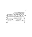
- FIG. 6 is a cross-sectional view showing a schematic configuration of the TFT array substrate.
- the gate bus line metal 40 first metal, first metal layer M1
- the first insulating layer I1 is formed thereon.
- a gate insulating film 50, a source bus line metal 42 (second metal) as the second metal layer M2, and an interlayer insulating film 52 as the second insulating layer I2 are provided in this order.
- wirings (metal wirings) by the respective metals are routed in various ways.
- Patent Documents 1 and 2 Therefore, various techniques have been proposed for suppressing the metal corrosion.
- Patent Document 1 in order to suppress the occurrence of corrosion of electrodes and the like, a technique for disposing a sealing material so as to prevent contact between a connection electrode for connecting a test thin film transistor and a test wiring and liquid crystal Is described.
- Patent Document 2 listed below describes a technique in which a connection portion between a power supply wiring and a power supply pad, which is a portion where metal is exposed, is disposed on the inner side of the outer edge of the seal region in order to suppress corrosion. Yes. Japanese Patent Publication “Japanese Patent Laid-Open No. 2002-12882 (Publication Date: April 26, 2002)” Japanese Patent Publication “JP 2007-24963 A (publication date: February 1, 2007)” Japanese Patent Publication “Japanese Patent Laid-Open No. 2006-276287 (Publication Date: October 12, 2006)”
- the conventional TFT array substrate has a problem that metal corrosion is not sufficiently suppressed. This will be described below with reference to the drawings.
- FIG. 7A is a plan view showing a wiring state of the TFT array substrate 20.
- a plurality of gate bus line metals 40a, 40b, and 40c are arranged in parallel in the X direction (see arrow X in FIG. 7A) that is the vertical direction of the insulating substrate 30.
- gate bus line metal 40b When one of them (gate bus line metal 40b) is skipped and two of the two sides (gate bus line metal 40a, 40b) sandwiching it are electrically connected explain.
- the gate bus line metals 40a, 40b, and 40c are formed on the insulating substrate 30 as first metals. Are formed in the same layer, that is, in the first metal layer M1.
- the gate bus line metal 40a and the gate bus line metal 40c are connected to each other.
- the gate bus line metal 40b needs to be connected through a different layer.
- a source bus line metal 42 (second metal) which is an upper layer through a gate insulating film 50 which is the first insulating layer I1 is formed from the first metal layer M1 where the gate bus line metal 40 is formed.
- a wiring is drawn out from the two metal layers M2 (see the connection region R10 in FIG. 7A), and the gate bus line metal 40a and the gate bus line metal 40c are connected by the second metal layer M2. Conceivable.
- connection region R10 As a method of connecting the first metal layer M1 and the second metal layer M2, a method of connecting using a via (via connection) and a method of using a third metal (via a third metal layer). There is a method of connection (third metal connection).
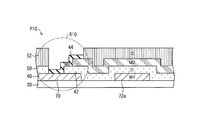
- FIG. 8 is a cross-sectional view showing a schematic configuration of the TFT array substrate 20.
- a via 46 penetrating the gate insulating film 50 is formed in a portion where the gate bus line metal 40 and the source bus line metal 42 overlap.
- the gate bus line metal 40 and the source bus line metal 42 are electrically connected through the via 46.
- first metal layer M1 and the second metal layer M2 are connected by the via 46 penetrating the first insulating layer I1.
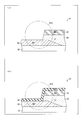
- FIGS. 9A and 9B both (a) and (b) of FIG. 9 are cross-sectional views showing a schematic configuration of the TFT array substrate 20, and (a) of FIG. 9B shows the structure following the TFT array substrate 20 shown in FIG. 6, and FIG. 9B shows the structure following FIG. 9A.
- an interlayer is formed as the second insulating layer I2.
- the insulating film 52 is removed to expose the source bus line metal 42 of the second metal layer M2.
- the gate insulating film 50 of the first insulating layer I1 is removed, and the gate bus line metal 40 is exposed.
- a pixel electrode metal 44 (third metal) as a third metal layer M3 is formed in the connection region R10 of the TFT array substrate 20.
- a pixel electrode metal 44 (third metal) as a third metal layer M3 is formed in the connection region R10 of the TFT array substrate 20.
- the gate bus line metal 40 of the first metal layer M1 and the source bus line metal 42 of the second metal layer M2 are electrically connected by the pixel electrode metal 44 of the third metal layer M3.
- This third metal connection has advantages in terms of manufacturing, such as a reduction in the number of processes compared to the via connection. Specifically, for example, a step of forming a via hole in order to form the via 46 can be omitted.
- the interlayer insulating film 52 as the second insulating layer I2, the source bus line metal 42 as the second metal layer M2, and the interlayer insulating film 52 as the first insulating layer I1 are successively patterned. By doing so, the third metal connection can be easily formed.
- the pixel electrode metal 44 is generally a thin film metal layer such as an ITO (Indium Tin Oxide) thin film. Therefore, even if the source bus line metal 42 as the second metal layer M2 is covered with the pixel electrode metal 44, it is easily corroded.
- ITO Indium Tin Oxide
- FIG. 10 is a plan view showing a schematic configuration of the peripheral portion of the TFT array substrate 20.
- the central portion thereof is a display region A ⁇ b> 10 in a plan view, and the peripheral region A ⁇ b> 20 in which the vicinity of the edge 24 of the surrounding TFT array substrate 20 is provided with the drive circuit 60 and the like. It becomes.
- a gate drive circuit 62 is provided as the drive circuit 60 at the left and right positions of the display area A10, the gate drive circuit 62 is connected to each line of the display area A10 and the gate bus line 41. Etc. are connected.
- the driver 100 and the gate drive circuit 62 are connected by a gate drive circuit signal line 110 such as a clock line, They are connected to each wiring in the display area A10 by the source bus line 43 or the like.
- the TFT array substrate 20 and the counter substrate are bonded together via a seal 90.
- the seal 90 is formed in a frame shape inside the TFT array substrate 20 along the edge 24.
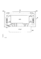
- FIG. 11 showing the peripheral area A20 of the TFT array substrate 20.
- a drive circuit 60 is formed in the peripheral area A20 of the TFT array substrate 20 so as to face the display area A10.
- wirings such as a low potential side power supply line (Vss) 70 and a clock wiring (CK) 72 are formed. These wirings and the drive circuit 60 may be connected in the horizontal direction of the TFT array substrate 20, that is, in the direction of the arrow X.
- the clock wiring 72 is formed in parallel as a plurality of clock wirings 72a and 72b, etc., and when it is necessary to connect across adjacent wirings, first, The third metal connection described based on FIG. 9B is formed.
- the low-potential side power supply line 70 and the drive circuit 60 in FIG. 11 are connected without contacting the clock wirings 72 formed therebetween, the low-potential side The third metal connection is formed on the power supply line 70 (see the connection point P10 in FIG. 11).
- the clock wirings 72a and 72b are in contact with each other by straddling adjacent clock wirings 72a and 72b formed in the same first metal layer M1 as the low potential side power supply line 70 via the second metal layer M2.
- the low-potential-side power supply line 70 and the drive circuit 60 are connected without causing them.
- the third metal connection is formed as necessary.
- the third metal that connects the first metal layer M1 and the second metal layer M2 is likely to be exposed.
- the pixel electrode metal 44 is generally a thin film metal layer such as an ITO (Indium Tin Oxide) thin film. Therefore, even if the source bus line metal 42 as the second metal layer M ⁇ b> 2 is covered with the pixel electrode metal 44, it easily corrodes.
- ITO Indium Tin Oxide
- connection point P10 where the third metal connection is formed is covered with the seal 90 is used.
- connection region R10 where the third metal connection is formed is covered with the seal 90, the third metal layer M3 is prevented from being directly in contact with the outside air.
- connection point P10 where the third metal connection is formed is formed in the vicinity of the edge 24 of the TFT array substrate 20 as shown in FIG. That is, various wirings such as the low-potential-side power supply line 70 and the clock wiring 72 in the peripheral region A20 are outside the various driving circuits 60, in other words, the various driving circuits 60 and the edges of the TFT array substrate 20. 24.
- various wirings such as the drive circuit 60, the low-potential-side power supply line 70, the clock wiring 72, and the like are directed toward the edge 24 of the TFT array substrate 20 following the display area A 10 in the center portion of the TFT array substrate 20. Arranged in order.
- the seal 90 has a certain width (D1 shown in FIG. 11, from the seal inner end 92 of the seal 90 to the seal outer end 94 in order to fully exert the function of bonding the TFT array substrate and the counter substrate together. Distance) is required.
- connection point P10 closest to the edge 24 of the TFT array substrate 20 among the group of connection points P10 is used. It is necessary to ensure a certain width from the position (first seal reference position, K1 in FIG. 11) to the seal outer end 94 of the seal 90 (D2, outer edge seal width shown in FIG. 11).
- connection points P10 where the third metal connection is formed are covered. Therefore, in determining the position of the seal 90, the position of the connection point P10 farthest from the end 24 of the TFT array substrate 20 among the group of connection points P10 (second seal reference position, K2 in FIG. 11). A configuration in which the position of the seal 90 is determined so as to cover the surface is also conceivable. In such a configuration, all of the group of connection points P10 where the third metal connection is formed are covered.
- the seal 90 is disposed at a position and width that includes the second seal reference position after securing a certain seal width D1 from the first seal reference position K1.
- the frame width of the TFT array substrate 20 in the display device is as shown by D3 in FIG.
- the frame means an area where display is not performed due to the arrangement of the seal 90 and the drive circuit 60 around the display device.
- the conventional configuration has a problem that the frame width D3 is wide, for example, as shown in FIG. That is, in the conventional arrangement shown in FIG. 11, the frame is close to the combined width of the drive circuit 60 and the seal width D1.
- the seal width D1 also includes the first seal reference position K1 and, depending on the configuration, the second seal reference position K2, and further, the seal width D1 from the first seal reference position K1 to the seal outer end 94 is further increased. Since the outer edge seal width D2 was included, the width was wide.
- Patent Document 3 describes a technique in which a part of a drive circuit is covered with a seal material in order to narrow a display device.
- Patent Document 3 it is possible to reduce the width from the outer edge of the seal to the edge of the substrate, but by forming a seal, a drive circuit, or the like other than the display area. The reduction of the frame, which is an area where no display is performed, was insufficient.
- the present invention has been made in view of the above problems, and an object thereof is to provide a TFT array substrate having a narrow frame. Another object of the present invention is to provide a TFT array substrate with a narrow frame while suppressing metal corrosion.
- the TFT array substrate of the present invention is TFT elements are provided in a matrix on an insulating substrate, On the insulating substrate, a gate bus line and a source bus line connected to the TFT element are provided by a first metal and a second metal, respectively.
- the first metal and the second metal are provided in different layers on the insulating substrate via an insulating layer,
- a connection point where the first metal and the second metal are electrically connected is provided in a peripheral region of the TFT element region, which is a region where the TFT elements are arranged in a matrix.
- the peripheral area is a TFT array substrate provided with a drive circuit for driving the TFT element, In the peripheral region, at least a part of the drive circuit is provided between the connection point and an end side of the insulating substrate.
- the drive circuit is formed outside the point (connection point) where different metal layers on the insulating substrate are connected in the peripheral region of the TFT array substrate.
- a seal or the like having a desired width is formed at least outside the connection point in consideration of misalignment or the like. Is done.
- the drive circuit is provided outside the said connection point. Therefore, it is possible to suppress the widening of the frame due to the provision of a seal or the like.
- a TFT array substrate with a narrow frame can be provided.
- the TFT array substrate of the present invention is The exposed third metal is preferably isolated from the atmosphere by an insulating material.
- the underlying metal may corrode when exposed to the atmosphere or the like.
- the exposed metal is isolated from the atmosphere by the insulating material, so that the metal is hardly corroded.
- the TFT array substrate of the present invention is In the peripheral region, a plurality of the connection points are provided, The exposed third metal in at least a part of the connection point may be isolated from the atmosphere by being covered with an insulating material.
- the TFT array substrate of the present invention is The exposed third metal at all the connection points can be isolated from the atmosphere by being covered with an insulating material.
- At least a part, preferably all, of the exposed third metal is isolated from the atmosphere by being covered with the insulating material, so that the corrosion of the metal is more reliably suppressed. can do.
- the TFT array substrate of the present invention is The peripheral region is provided with an insulating material, By providing the insulating material closer to the edge of the insulating substrate than the exposed third metal at all the connection points, The exposed third metal may be isolated from the atmosphere.
- the TFT array substrate of the present invention is The exposed third metal at all the connection points is It can be surrounded by the insulating material provided along the edge of the insulating substrate.
- the insulating material is not in contact with the exposed third metal and connection point.
- interval (gap) between the said insulating substrate and a counter substrate is easy to be kept constant.
- variation in the thickness of the liquid crystal layer sandwiched between the substrates can be suppressed.
- a conductive material is mixed in the insulating material (for example, a conductive material mixed sealing material)
- the material is not in contact with the exposed third metal, an electrical leak (for example, the facing Conduction with the counter electrode of the substrate) can be suppressed.
- the TFT array substrate of the present invention is The peripheral region is provided with an insulating material,
- the insulating material may cover the drive circuit provided between the connection point and the edge of the insulating substrate in the peripheral region.
- the seal is provided so as to cover the drive circuit provided in the peripheral region. Therefore, the expansion of the frame due to the provision of the seal can be further suppressed.
- the TFT array substrate of the present invention is In the peripheral region, the drive circuit provided between the connection point and the edge of the insulating substrate may be provided with at least one of a three-terminal element, a resistor element, and a capacitor element.
- the TFT array substrate of the present invention is In the peripheral region, a three-terminal element, a resistor element, and a capacitor element can be provided in the drive circuit provided between the connection point and the edge of the insulating substrate.
- the TFT array substrate of the present invention is In the peripheral region, at least one signal line extending in the same direction as the edge of the insulating substrate in the peripheral region is formed, At least a part of the drive circuit can be provided between the signal line and the edge of the insulating substrate.
- elements essential to the circuit configuration such as a three-terminal element, a resistance element, and a capacitive element are provided in the drive circuit and the like.
- connection point is easy to be formed in a wide range.
- the drive circuit is formed in the outer side of this connection point, the expansion of a frame can be suppressed. .
- the TFT array substrate of the present invention is
- the signal line includes a clock wiring and a DC power supply line for supplying a potential for turning off the TFT element.
- the DC power supply line can be formed between the drive circuit and an edge of the insulating substrate in the peripheral region.
- the TFT array substrate of the present invention is In the peripheral region, the wiring formed of the first metal and the wiring formed of the second metal cross through the insulating layer in a plan view, In the intersecting region, the substantial width of the wiring of at least one of the wiring formed by the first metal and the wiring formed by the second metal can be reduced.
- the TFT array substrate of the present invention is In the peripheral region, the wiring formed of the first metal and the wiring formed of the second metal cross through the insulating layer in a plan view, In the crossing region, a part of at least one of the wiring formed by the first metal and the wiring formed by the second metal can be cut out.
- the substantial width of the wiring means not the apparent maximum width of the wiring but the effective width (the width of the region where the metal is formed) in the direction orthogonal to the extending direction of the wiring.
- the substantial width means the width of the metal excluding the cutout portion.
- the TFT array substrate of the present invention is The insulating substrate is bonded to a counter substrate through a seal, An insulating material covering the third metal can be used as the seal.
- the insulating material covering the third metal is a seal for bonding to the counter substrate, corrosion of the metal can be suppressed without particularly increasing the number of steps.
- the TFT array substrate of the present invention is A pixel electrode connected to the TFT element is formed in the TFT element region,
- the third metal may be a metal that forms the pixel electrode.
- the third metal is a metal for forming the pixel electrode, the first metal and the second metal can be connected without particularly increasing the number of steps.
- the TFT array substrate of the present invention is In the peripheral region, the drive circuit provided between the connection point and the edge of the insulating substrate includes a three-terminal element,
- the three-terminal element can be an element that outputs a signal to the TFT element.
- the TFT array substrate of the present invention is The three-terminal element can constitute a pull-up circuit for outputting an ON signal to the TFT element.
- the TFT array substrate of the present invention is The three-terminal element can constitute a pull-down circuit for outputting an OFF signal to the TFT element.
- the TFT array substrate of the present invention is In the peripheral region, a bootstrap capacitor element can be provided in the drive circuit provided between the connection point and the edge of the insulating substrate.
- an element that outputs a signal to the TFT element particularly a pull-up circuit or a pull-down circuit, or a relatively large circuit such as a bootstrap capacitor element is formed in the drive circuit. Has been.
- the liquid crystal display device of the present invention is The TFT array substrate can be provided.
- the frame of the liquid crystal display device can be narrowed.
- the TFT array substrate 20 of the present invention is characterized in that at least a part of the drive circuit is provided in the peripheral region between the connection point and the edge of the insulating substrate.
- the TFT array substrate having a narrow frame can be provided.
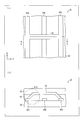
- FIG. 1 showing an embodiment of the present invention, is a diagram showing a schematic configuration of a TFT array substrate.
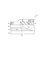
- FIG. FIG. 2 is a view corresponding to a cross section taken along line AA in FIG. 1.
- FIG. 2 is a view corresponding to a cross section taken along line BB in FIG. 1.
- FIG. 1 shows schematic structure of the drive circuit of this invention.
- Another embodiment of the present invention is shown and is a diagram showing a schematic configuration of a TFT array substrate.
- FIG. It is sectional drawing which shows schematic structure of a TFT array substrate. It is a figure which shows the mode of wiring of a TFT array substrate, (a) is a plane, (b) has shown the VV sectional view of (a).
- FIG. 6 It is sectional drawing which shows schematic structure of a TFT array substrate. It is sectional drawing which shows schematic structure of a TFT array substrate, (a) shows the structure following the said FIG. 6, (b) has shown the structure following the said figure (a). It is a top view which shows schematic structure of a TFT array substrate. It is a figure which shows schematic structure of the peripheral region of a TFT array substrate.
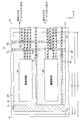
- FIG. 1 is a diagram showing a schematic configuration of the TFT array substrate of the present embodiment.
- the drive circuit 60 is divided into a drive circuit A 60a and a drive circuit B 60b. Yes.
- the low potential side power supply line 70 and the clock wiring 72a which are provided adjacent to each other in the Y direction and serve as a DC power supply line for supplying a potential for turning off the TFT elements.
- 72b is divided into a low-potential side power supply line 70 and clock wirings 72a and 72b.
- a drive circuit B60b of the drive circuit 60 divided into the two is provided.
- the display area A10 as the TFT element area at the center thereof is followed by the TFT array substrate 20 Various wirings such as the drive circuit 60, the low-potential-side power supply line 70, and the clock wiring 72 are arranged in this order toward the end 24.
- the drive circuit A 60 a is first arranged toward the end side 24 of the TFT array substrate 20 following the display area A 10 in the center of the TFT array substrate 20, and then A part of various wirings extending in the Y direction, specifically, clock wirings 72a and 72b are provided. Subsequently, a drive circuit B 60 b which is the other of the divided drive circuits 60 is arranged, and a low-potential side power line 70 is provided between the drive circuit B 60 b and the TFT array substrate 20.
- the wiring extending in the X direction for connecting each wiring extended in the Y direction and the driving circuit 60 is mainly between the driving circuit A 60a and the driving circuit B 60b. Crosses the wiring extending in the Y direction.
- the location where the wiring extended in the X direction needs to cross the wiring extended in the Y direction and straddle the wiring extended in the Y direction is between the drive circuit A 60a and the drive circuit B 60b. Mainly occurs between.
- the third metal connection structure described above with reference to FIG. 9B is also mainly formed between the drive circuit A 60a and the drive circuit B 60b. Specifically, the third metal connection is formed at the point P10 which is the connection point shown in FIG.
- connection point P10 where the third metal connection is formed with a seal 90 and isolate it from the atmosphere.
- connection points P10 where the wirings and the third metal connection are formed it is necessary to cover the connection points P10 where the wirings and the third metal connection are formed, while securing a margin for a positional deviation or the like when the seal 90 is formed on the substrate.
- the seal 90 can be disposed so that the overlap between the seal 90 and the drive circuit 60 is increased. That is, in the present embodiment, the seal point from the second seal reference position K2, which is the point closest to the display area A10 among the connection points P10, in other words, the point farthest from the edge 24 of the TFT array substrate 20.
- One of the divided drive circuits 60, that is, the drive circuit B 60b is formed while reaching the outer end 94.
- the seal 90 overlaps not only each connection point P10 and each wiring such as the low potential side power supply line 70 but also the driving circuit B60b.
- the distance from the display area A10 to the seal outer end 94 can be shortened.
- the frame that can be placed on the TFT array substrate 20 can be narrowed.
- the frame means an area where display is not performed due to the arrangement of the seal 90 and the drive circuit 60 around the display device.
- the size of the drive circuit 60 formed in the region other than the seal 90 can be reduced while the seal width D1 is not greatly increased and is equal or rather narrowed. .
- the distance from the display area A10 in the TFT array substrate 20 to the seal inner end 92 can be shortened, and in turn, the distance from the display area A10 to the seal outer end 94 can be further shortened. .
- the drive circuit 60 is divided into a plurality of parts, and a part thereof is covered with the seal 90, whereby the frame can be narrowed. Further, since the connection point P10 where the third metal connection is formed is covered with the seal 90, corrosion of the metal can be suppressed.
- the driving circuit A 60a and the like are not connected from the low-potential-side power supply line 70 formed in the first metal layer M1 to the clock wiring 72a similarly formed in the first metal layer M1.
- the first metal layer M1 and the second metal layer M2 are formed by the third metal connection structure described above, that is, the third metal such as the pixel electrode metal. Is formed.
- the metal is exposed.
- the metal is not easily corroded because it is covered with the seal 90 as described above.
- the second metal layer M2 bypasses the wiring of the first metal layer M1, and after straddling it, the first metal is connected again by the same third metal connection structure. Can be connected to layer M1.
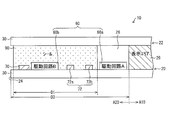
- FIG. 3 is a view corresponding to the cross section taken along the line BB of FIG. 1 when the TFT array substrate of the present embodiment is used in a liquid crystal display device.
- the liquid crystal display device 10 has a structure in which the liquid crystal layer 26 is sandwiched between two insulating substrates 30 facing each other.
- liquid crystal layer 26 is sandwiched between the TFT array substrate 20 on which the drive circuit 60 is formed and the counter substrate 22.
- the TFT array substrate 20 and the counter substrate 22 are fixed to each other in a bonded state, and further, a so-called gap, which is a distance between the TFT array substrate 20 and the counter substrate 22, is maintained at a desired value. , A seal 90 is provided.
- the drive circuit 60 is divided into a drive circuit A 60a and a drive circuit B 60b, and a signal line is provided between the drive circuit A 60a and the drive circuit B 60b.
- Clock wirings 72a and 72b are formed.
- a low-potential-side power supply line 70 as a kind of signal line is provided between the drive circuit B 60 b and the edge 24 of the TFT array substrate 20.
- the low-potential-side power line 70 is provided outside the drive circuit 60. A stable voltage can be supplied.
- the clock wirings 72 a and 72 b are covered with a seal 90. Therefore, the connection point P10 (see FIG. 1 and the like) formed on the clock wirings 72a and 72b is covered with the seal 90.
- the seal 90 is made of an insulating material. Therefore, the structure of the third metal connection formed at the connection point P10 is covered with the insulating material.
- the exposed portion of the metal formed in the connection region R10 in the third metal connection is covered with the insulating material and is not directly in contact with the outside air. Therefore, corrosion of the metal in the third metal connection can be suppressed.
- the clock wiring 72 formed between the drive circuit A 60a and the drive circuit B 60b is shown covered with the seal 90.
- the configuration of the display device 10 is not limited to such a configuration, and a configuration that covers only a part thereof is also possible.
- the clock wiring 72 may be formed with a third metal connection having a metal exposed portion.
- the clock wiring 72 is covered with a seal material in which a conductive material is mixed into the seal 90, the exposed third metal placed on the third metal connection and the counter substrate 22 formed on the counter substrate 22 are opposed to each other. There is a possibility that the electrode is electrically connected to the electrode through the conductive seal 90.
- seal 90 As an example of the arrangement of the seal 90 as described above, for example, an arrangement in which the seal 90 as an insulating material is provided closer to the end 24 of the insulating substrate 30 than the third metal exposed at the connection point. Conceivable.
- the seal 90 can be provided along the edge 24 of the insulating substrate 30, and the exposed third metal can be enclosed inside the seal 90.
- the seal 90 of the present invention is arranged so as to cover all of the exposed third metal, or a part thereof, or so as not to cover any of them. Can be arranged.
- FIG. 4 is a diagram showing a schematic configuration of the drive circuit in the present embodiment.
- the pull-up / pull-down control means 132, the pull-up means 134, and the pull-down means 136 are the main components and function as a shift register.
- the pull-up means 134 and the pull-down means 136 mean a circuit (pull-up circuit, pull-down circuit) constituted by a three-terminal element or the like.
- the pull-up / pull-down control means 132 receives a control signal such as a clock signal (CK) or a set signal from one or more previous stages. Depending on the configuration, the pull-up / pull-down control means 132 outputs a reset signal to one or more previous stages.
- CK clock signal
- the pull-up / pull-down control means 132 outputs a reset signal to one or more previous stages.
- the pull-up / pull-down control means 132 controls the pull-up means 134 and the pull-down means 136 connected to the pull-up / pull-down control means 132.
- the pull-up / pull-down control means 132 controls the pull-up means 134 connected to Vdd to which a high voltage of the clock is supplied, and the display as an active area.
- a voltage (ON signal) for turning on a driving element such as a TFT element is supplied, or a pull-down means 136 connected to Vss to which a low voltage of a clock, a low voltage of DC, etc. are supplied is controlled.
- a voltage for turning off a driving element such as a TFT element in the display area A10 as an active area (OFF signal) is supplied.
- the pull-up means is used to change the source potential or the drain potential.
- a so-called bootstrap capacitor that increases the gate potential of the means may be provided.
- an element provided in the drive circuit B 60b provided between the clock wiring 72 and the low-potential-side power line 70 in FIG. 1 is not particularly limited.
- a three-terminal element, a resistor element, a capacitor element, or the like Provided.
- the circuit provided in the drive circuit B60b is more effective from the viewpoint of reducing the frame width when the size is larger.
- the bootstrap capacitor described above is provided, it is also effective to dispose a circuit element (bootstrap capacitor) related to the capacitor formation in the drive circuit B60b.
- FIG. 5 shows an embodiment of the present invention and is a diagram showing a schematic configuration of the TFT array substrate 20.
- the drive circuit 60 is not divided, and one drive circuit is provided between the low-potential-side power supply line 70 that is a kind of signal line and the clock wiring 72 in the peripheral region A20. Is provided.
- the frame width D ⁇ b> 3 can be reduced, and by covering the connection point P ⁇ b> 10 with the seal 90, metal corrosion can also be suppressed.
- the substantial width of the wiring in the crossing region can be narrowed by hollowing out a part of the wiring.
- the frame In the TFT array substrate, the frame can be narrowed and metal corrosion can be suppressed, so that it can be suitably used for display devices such as liquid crystal display devices, sensors, and the like.
Landscapes
- Physics & Mathematics (AREA)
- Nonlinear Science (AREA)
- Mathematical Physics (AREA)
- Chemical & Material Sciences (AREA)
- Crystallography & Structural Chemistry (AREA)
- General Physics & Mathematics (AREA)
- Optics & Photonics (AREA)
- Engineering & Computer Science (AREA)
- Microelectronics & Electronic Packaging (AREA)
- Liquid Crystal (AREA)
- Devices For Indicating Variable Information By Combining Individual Elements (AREA)
Abstract
Priority Applications (2)
| Application Number | Priority Date | Filing Date | Title |
|---|---|---|---|
| CN200880123410.8A CN101910932B (zh) | 2008-04-17 | 2008-12-02 | Tft阵列基板和液晶显示装置 |
| US12/811,343 US20100283931A1 (en) | 2008-04-17 | 2008-12-02 | Tft array substrate and liquid crystal display device |
Applications Claiming Priority (2)
| Application Number | Priority Date | Filing Date | Title |
|---|---|---|---|
| JP2008-107959 | 2008-04-17 | ||
| JP2008107959 | 2008-04-17 |
Publications (1)
| Publication Number | Publication Date |
|---|---|
| WO2009128179A1 true WO2009128179A1 (fr) | 2009-10-22 |
Family
ID=41198891
Family Applications (1)
| Application Number | Title | Priority Date | Filing Date |
|---|---|---|---|
| PCT/JP2008/071843 Ceased WO2009128179A1 (fr) | 2008-04-17 | 2008-12-02 | Substrat de matrice tft et dispositif d'affichage à cristaux liquides |
Country Status (3)
| Country | Link |
|---|---|
| US (1) | US20100283931A1 (fr) |
| CN (1) | CN101910932B (fr) |
| WO (1) | WO2009128179A1 (fr) |
Cited By (5)
| Publication number | Priority date | Publication date | Assignee | Title |
|---|---|---|---|---|
| WO2011086782A1 (fr) * | 2010-01-13 | 2011-07-21 | シャープ株式会社 | Substrat matriciel et panneau d'affichage à cristaux liquides |
| WO2011132440A1 (fr) * | 2010-04-22 | 2011-10-27 | シャープ株式会社 | Substrat de matrice active et dispositif d'affichage |
| US8723845B2 (en) | 2010-02-08 | 2014-05-13 | Sharp Kabushiki Kaisha | Display device |
| JPWO2013172243A1 (ja) * | 2012-05-16 | 2016-01-12 | シャープ株式会社 | 液晶ディスプレイ |
| US9385143B2 (en) * | 2009-02-16 | 2016-07-05 | Sharp Kabushiki Kaisha | TFT array substrate, and liquid crystal display panel |
Families Citing this family (9)
| Publication number | Priority date | Publication date | Assignee | Title |
|---|---|---|---|---|
| JP6092551B2 (ja) * | 2012-09-07 | 2017-03-08 | 株式会社ジャパンディスプレイ | 表示パネル |
| CN104020593A (zh) * | 2014-05-30 | 2014-09-03 | 深圳市华星光电技术有限公司 | 阵列基板、制作方法及液晶显示面板 |
| CN107134264B (zh) | 2016-02-26 | 2020-08-14 | 瀚宇彩晶股份有限公司 | 驱动电路和显示装置 |
| CN106842733B (zh) * | 2017-02-13 | 2019-03-15 | 深圳市华星光电技术有限公司 | 显示面板及其阵列基板 |
| EP3816975A4 (fr) * | 2018-06-29 | 2022-07-06 | Kyocera Corporation | Dispositif d'affichage |
| KR102612390B1 (ko) * | 2018-12-19 | 2023-12-12 | 엘지디스플레이 주식회사 | 표시 패널 및 표시 장치 |
| CN112820763B (zh) | 2019-07-31 | 2024-06-28 | 京东方科技集团股份有限公司 | 电致发光显示面板及显示装置 |
| AU2019279939B2 (en) * | 2019-07-31 | 2021-04-08 | Boe Technology Group Co., Ltd. | Display substrate and display device |
| CN113359359B (zh) * | 2021-04-20 | 2023-08-25 | 绵阳惠科光电科技有限公司 | 一种显示面板和显示装置 |
Citations (3)
| Publication number | Priority date | Publication date | Assignee | Title |
|---|---|---|---|---|
| JP2000081636A (ja) * | 1998-09-03 | 2000-03-21 | Seiko Epson Corp | 電気光学装置及びその製造方法並びに電子機器 |
| JP2008003134A (ja) * | 2006-06-20 | 2008-01-10 | Mitsubishi Electric Corp | 配線構造、及び表示装置 |
| JP2008026865A (ja) * | 2006-07-21 | 2008-02-07 | Samsung Electronics Co Ltd | 表示基板及びこれを具備する表示装置 |
Family Cites Families (7)
| Publication number | Priority date | Publication date | Assignee | Title |
|---|---|---|---|---|
| JPH09311342A (ja) * | 1996-05-16 | 1997-12-02 | Semiconductor Energy Lab Co Ltd | 表示装置 |
| KR100244449B1 (ko) * | 1997-02-11 | 2000-02-01 | 구본준 | 박막 트랜지스터 검사용 단락 배선을 갖는 액정 표시 장치와 그 제조 방법(liquid crystal display having shorting bar for testing tft and method for manufacturing the same) |
| WO1999023530A1 (fr) * | 1997-10-31 | 1999-05-14 | Seiko Epson Corporation | Dispositif electro-optique et appareil electronique |
| US6049365A (en) * | 1998-05-07 | 2000-04-11 | Mitsubishi Denki Kabushiki Kaisha | Liquid crystal displaying apparatus with a converter not exposed to liquid crystal |
| JP4342711B2 (ja) * | 2000-09-20 | 2009-10-14 | 株式会社日立製作所 | 液晶表示装置の製造方法 |
| KR101085137B1 (ko) * | 2004-12-23 | 2011-11-21 | 엘지디스플레이 주식회사 | 액정 표시 패널 및 그 제조방법 |
| US7385441B2 (en) * | 2006-09-27 | 2008-06-10 | Tpo Displays Corp. | Level shifter with reduced power consumption |
-
2008
- 2008-12-02 WO PCT/JP2008/071843 patent/WO2009128179A1/fr not_active Ceased
- 2008-12-02 CN CN200880123410.8A patent/CN101910932B/zh not_active Expired - Fee Related
- 2008-12-02 US US12/811,343 patent/US20100283931A1/en not_active Abandoned
Patent Citations (3)
| Publication number | Priority date | Publication date | Assignee | Title |
|---|---|---|---|---|
| JP2000081636A (ja) * | 1998-09-03 | 2000-03-21 | Seiko Epson Corp | 電気光学装置及びその製造方法並びに電子機器 |
| JP2008003134A (ja) * | 2006-06-20 | 2008-01-10 | Mitsubishi Electric Corp | 配線構造、及び表示装置 |
| JP2008026865A (ja) * | 2006-07-21 | 2008-02-07 | Samsung Electronics Co Ltd | 表示基板及びこれを具備する表示装置 |
Cited By (15)
| Publication number | Priority date | Publication date | Assignee | Title |
|---|---|---|---|---|
| US9385143B2 (en) * | 2009-02-16 | 2016-07-05 | Sharp Kabushiki Kaisha | TFT array substrate, and liquid crystal display panel |
| US9733538B2 (en) | 2009-02-16 | 2017-08-15 | Sharp Kabushiki Kaisha | TFT array substrate, and liquid crystal display panel |
| US8686980B2 (en) | 2010-01-13 | 2014-04-01 | Sharp Kabushiki Kaisha | Array substrate and liquid crystal display panel |
| JPWO2011086782A1 (ja) * | 2010-01-13 | 2013-05-16 | シャープ株式会社 | アレイ基板、及び、液晶表示パネル |
| RU2495498C1 (ru) * | 2010-01-13 | 2013-10-10 | Шарп Кабусики Кайся | Подложка матрицы и жидкокристаллическая панель отображения |
| KR101377891B1 (ko) | 2010-01-13 | 2014-03-25 | 샤프 가부시키가이샤 | 어레이 기판 및 액정 표시 패널 |
| WO2011086782A1 (fr) * | 2010-01-13 | 2011-07-21 | シャープ株式会社 | Substrat matriciel et panneau d'affichage à cristaux liquides |
| CN102713998B (zh) * | 2010-01-13 | 2014-07-09 | 夏普株式会社 | 阵列基板和液晶显示面板 |
| EP2525343A4 (fr) * | 2010-01-13 | 2015-08-19 | Sharp Kk | Substrat matriciel et panneau d'affichage à cristaux liquides |
| CN102713998A (zh) * | 2010-01-13 | 2012-10-03 | 夏普株式会社 | 阵列基板和液晶显示面板 |
| US8723845B2 (en) | 2010-02-08 | 2014-05-13 | Sharp Kabushiki Kaisha | Display device |
| US9244317B2 (en) | 2010-04-22 | 2016-01-26 | Sharp Kabushiki Kaisha | Active matrix substrate and display device |
| WO2011132440A1 (fr) * | 2010-04-22 | 2011-10-27 | シャープ株式会社 | Substrat de matrice active et dispositif d'affichage |
| JPWO2013172243A1 (ja) * | 2012-05-16 | 2016-01-12 | シャープ株式会社 | 液晶ディスプレイ |
| US10838259B2 (en) | 2012-05-16 | 2020-11-17 | Sharp Kabushiki Kaisha | Liquid crystal display |
Also Published As
| Publication number | Publication date |
|---|---|
| CN101910932B (zh) | 2013-06-05 |
| CN101910932A (zh) | 2010-12-08 |
| US20100283931A1 (en) | 2010-11-11 |
Similar Documents
| Publication | Publication Date | Title |
|---|---|---|
| WO2009128179A1 (fr) | Substrat de matrice tft et dispositif d'affichage à cristaux liquides | |
| US7893436B2 (en) | Array substrate, display apparatus having the same | |
| US9244317B2 (en) | Active matrix substrate and display device | |
| CN102713998B (zh) | 阵列基板和液晶显示面板 | |
| JP2007316104A (ja) | 表示装置 | |
| JP2008032920A (ja) | 液晶表示装置 | |
| US8686446B2 (en) | Capacitor device and display apparatus having the same | |
| US10884542B2 (en) | Display device | |
| US9812469B2 (en) | Array substrate having a plurality of gate electrode material lines, source-drain electrode material lines and first metal lines | |
| JP4815868B2 (ja) | 表示装置 | |
| JP2011017821A (ja) | 液晶表示パネル及びその製造方法 | |
| JP2008064961A (ja) | 配線構造、及び表示装置 | |
| JP4170235B2 (ja) | 表示装置 | |
| JP5626112B2 (ja) | 表示装置 | |
| WO2007111044A1 (fr) | Affichage a cristaux liquides | |
| JP2008089646A (ja) | 表示装置 | |
| JP2007065150A (ja) | 液晶表示装置 | |
| KR101687718B1 (ko) | 액정표시장치 및 그 제조방법 | |
| JP5293240B2 (ja) | 表示装置 | |
| JP5655845B2 (ja) | 表示装置およびic | |
| JP5243278B2 (ja) | 液晶表示装置 | |
| JP2020060620A (ja) | 表示装置 | |
| JP2009244899A (ja) | 薄膜トランジスタパネルおよびその製造方法 | |
| JPH10253991A (ja) | 液晶表示装置 | |
| JP2009204949A (ja) | 表示装置 |
Legal Events
| Date | Code | Title | Description |
|---|---|---|---|
| WWE | Wipo information: entry into national phase |
Ref document number: 200880123410.8 Country of ref document: CN |
|
| 121 | Ep: the epo has been informed by wipo that ep was designated in this application |
Ref document number: 08873966 Country of ref document: EP Kind code of ref document: A1 |
|
| WWE | Wipo information: entry into national phase |
Ref document number: 12811343 Country of ref document: US |
|
| NENP | Non-entry into the national phase |
Ref country code: DE |
|
| 122 | Ep: pct application non-entry in european phase |
Ref document number: 08873966 Country of ref document: EP Kind code of ref document: A1 |
|
| NENP | Non-entry into the national phase |
Ref country code: JP |