WO2009128372A1 - Transistor à couche mince et procédé de fabrication associé - Google Patents
Transistor à couche mince et procédé de fabrication associé Download PDFInfo
- Publication number
- WO2009128372A1 WO2009128372A1 PCT/JP2009/057176 JP2009057176W WO2009128372A1 WO 2009128372 A1 WO2009128372 A1 WO 2009128372A1 JP 2009057176 W JP2009057176 W JP 2009057176W WO 2009128372 A1 WO2009128372 A1 WO 2009128372A1
- Authority
- WO
- WIPO (PCT)
- Prior art keywords
- layer
- gas
- metal
- film transistor
- thin film
- Prior art date
- Legal status (The legal status is an assumption and is not a legal conclusion. Google has not performed a legal analysis and makes no representation as to the accuracy of the status listed.)
- Ceased
Links
Images



Classifications
-
- H—ELECTRICITY
- H10—SEMICONDUCTOR DEVICES; ELECTRIC SOLID-STATE DEVICES NOT OTHERWISE PROVIDED FOR
- H10D—INORGANIC ELECTRIC SEMICONDUCTOR DEVICES
- H10D30/00—Field-effect transistors [FET]
- H10D30/60—Insulated-gate field-effect transistors [IGFET]
- H10D30/67—Thin-film transistors [TFT]
- H10D30/6729—Thin-film transistors [TFT] characterised by the electrodes
- H10D30/6737—Thin-film transistors [TFT] characterised by the electrodes characterised by the electrode materials
-
- H—ELECTRICITY
- H10—SEMICONDUCTOR DEVICES; ELECTRIC SOLID-STATE DEVICES NOT OTHERWISE PROVIDED FOR
- H10W—GENERIC PACKAGES, INTERCONNECTIONS, CONNECTORS OR OTHER CONSTRUCTIONAL DETAILS OF DEVICES COVERED BY CLASS H10
- H10W20/00—Interconnections in chips, wafers or substrates
- H10W20/40—Interconnections external to wafers or substrates, e.g. back-end-of-line [BEOL] metallisations or vias connecting to gate electrodes
- H10W20/41—Interconnections external to wafers or substrates, e.g. back-end-of-line [BEOL] metallisations or vias connecting to gate electrodes characterised by their conductive parts
- H10W20/425—Barrier, adhesion or liner layers
-
- C—CHEMISTRY; METALLURGY
- C23—COATING METALLIC MATERIAL; COATING MATERIAL WITH METALLIC MATERIAL; CHEMICAL SURFACE TREATMENT; DIFFUSION TREATMENT OF METALLIC MATERIAL; COATING BY VACUUM EVAPORATION, BY SPUTTERING, BY ION IMPLANTATION OR BY CHEMICAL VAPOUR DEPOSITION, IN GENERAL; INHIBITING CORROSION OF METALLIC MATERIAL OR INCRUSTATION IN GENERAL
- C23C—COATING METALLIC MATERIAL; COATING MATERIAL WITH METALLIC MATERIAL; SURFACE TREATMENT OF METALLIC MATERIAL BY DIFFUSION INTO THE SURFACE, BY CHEMICAL CONVERSION OR SUBSTITUTION; COATING BY VACUUM EVAPORATION, BY SPUTTERING, BY ION IMPLANTATION OR BY CHEMICAL VAPOUR DEPOSITION, IN GENERAL
- C23C14/00—Coating by vacuum evaporation, by sputtering or by ion implantation of the coating forming material
- C23C14/0021—Reactive sputtering or evaporation
- C23C14/0036—Reactive sputtering
- C23C14/0057—Reactive sputtering using reactive gases other than O2, H2O, N2, NH3 or CH4
-
- C—CHEMISTRY; METALLURGY
- C23—COATING METALLIC MATERIAL; COATING MATERIAL WITH METALLIC MATERIAL; CHEMICAL SURFACE TREATMENT; DIFFUSION TREATMENT OF METALLIC MATERIAL; COATING BY VACUUM EVAPORATION, BY SPUTTERING, BY ION IMPLANTATION OR BY CHEMICAL VAPOUR DEPOSITION, IN GENERAL; INHIBITING CORROSION OF METALLIC MATERIAL OR INCRUSTATION IN GENERAL
- C23C—COATING METALLIC MATERIAL; COATING MATERIAL WITH METALLIC MATERIAL; SURFACE TREATMENT OF METALLIC MATERIAL BY DIFFUSION INTO THE SURFACE, BY CHEMICAL CONVERSION OR SUBSTITUTION; COATING BY VACUUM EVAPORATION, BY SPUTTERING, BY ION IMPLANTATION OR BY CHEMICAL VAPOUR DEPOSITION, IN GENERAL
- C23C14/00—Coating by vacuum evaporation, by sputtering or by ion implantation of the coating forming material
- C23C14/06—Coating by vacuum evaporation, by sputtering or by ion implantation of the coating forming material characterised by the coating material
- C23C14/14—Metallic material, boron or silicon
- C23C14/18—Metallic material, boron or silicon on other inorganic substrates
- C23C14/185—Metallic material, boron or silicon on other inorganic substrates by cathodic sputtering
-
- H—ELECTRICITY
- H10—SEMICONDUCTOR DEVICES; ELECTRIC SOLID-STATE DEVICES NOT OTHERWISE PROVIDED FOR
- H10D—INORGANIC ELECTRIC SEMICONDUCTOR DEVICES
- H10D30/00—Field-effect transistors [FET]
- H10D30/01—Manufacture or treatment
- H10D30/021—Manufacture or treatment of FETs having insulated gates [IGFET]
- H10D30/031—Manufacture or treatment of FETs having insulated gates [IGFET] of thin-film transistors [TFT]
- H10D30/0312—Manufacture or treatment of FETs having insulated gates [IGFET] of thin-film transistors [TFT] characterised by the gate electrodes
- H10D30/0316—Manufacture or treatment of FETs having insulated gates [IGFET] of thin-film transistors [TFT] characterised by the gate electrodes of lateral bottom-gate TFTs comprising only a single gate
-
- H—ELECTRICITY
- H10—SEMICONDUCTOR DEVICES; ELECTRIC SOLID-STATE DEVICES NOT OTHERWISE PROVIDED FOR
- H10D—INORGANIC ELECTRIC SEMICONDUCTOR DEVICES
- H10D30/00—Field-effect transistors [FET]
- H10D30/60—Insulated-gate field-effect transistors [IGFET]
- H10D30/67—Thin-film transistors [TFT]
- H10D30/6729—Thin-film transistors [TFT] characterised by the electrodes
- H10D30/673—Thin-film transistors [TFT] characterised by the electrodes characterised by the shapes, relative sizes or dispositions of the gate electrodes
- H10D30/6732—Bottom-gate only TFTs
-
- H—ELECTRICITY
- H10—SEMICONDUCTOR DEVICES; ELECTRIC SOLID-STATE DEVICES NOT OTHERWISE PROVIDED FOR
- H10D—INORGANIC ELECTRIC SEMICONDUCTOR DEVICES
- H10D30/00—Field-effect transistors [FET]
- H10D30/60—Insulated-gate field-effect transistors [IGFET]
- H10D30/67—Thin-film transistors [TFT]
- H10D30/674—Thin-film transistors [TFT] characterised by the active materials
- H10D30/6741—Group IV materials, e.g. germanium or silicon carbide
- H10D30/6743—Silicon
-
- H—ELECTRICITY
- H10—SEMICONDUCTOR DEVICES; ELECTRIC SOLID-STATE DEVICES NOT OTHERWISE PROVIDED FOR
- H10W—GENERIC PACKAGES, INTERCONNECTIONS, CONNECTORS OR OTHER CONSTRUCTIONAL DETAILS OF DEVICES COVERED BY CLASS H10
- H10W20/00—Interconnections in chips, wafers or substrates
- H10W20/40—Interconnections external to wafers or substrates, e.g. back-end-of-line [BEOL] metallisations or vias connecting to gate electrodes
- H10W20/41—Interconnections external to wafers or substrates, e.g. back-end-of-line [BEOL] metallisations or vias connecting to gate electrodes characterised by their conductive parts
- H10W20/44—Conductive materials thereof
- H10W20/4403—Conductive materials thereof based on metals, e.g. alloys, metal silicides
- H10W20/4421—Conductive materials thereof based on metals, e.g. alloys, metal silicides the principal metal being copper
- H10W20/4424—Copper alloys
-
- H—ELECTRICITY
- H10—SEMICONDUCTOR DEVICES; ELECTRIC SOLID-STATE DEVICES NOT OTHERWISE PROVIDED FOR
- H10D—INORGANIC ELECTRIC SEMICONDUCTOR DEVICES
- H10D86/00—Integrated devices formed in or on insulating or conducting substrates, e.g. formed in silicon-on-insulator [SOI] substrates or on stainless steel or glass substrates
- H10D86/40—Integrated devices formed in or on insulating or conducting substrates, e.g. formed in silicon-on-insulator [SOI] substrates or on stainless steel or glass substrates characterised by multiple TFTs
- H10D86/441—Interconnections, e.g. scanning lines
-
- H—ELECTRICITY
- H10—SEMICONDUCTOR DEVICES; ELECTRIC SOLID-STATE DEVICES NOT OTHERWISE PROVIDED FOR
- H10D—INORGANIC ELECTRIC SEMICONDUCTOR DEVICES
- H10D86/00—Integrated devices formed in or on insulating or conducting substrates, e.g. formed in silicon-on-insulator [SOI] substrates or on stainless steel or glass substrates
- H10D86/40—Integrated devices formed in or on insulating or conducting substrates, e.g. formed in silicon-on-insulator [SOI] substrates or on stainless steel or glass substrates characterised by multiple TFTs
- H10D86/60—Integrated devices formed in or on insulating or conducting substrates, e.g. formed in silicon-on-insulator [SOI] substrates or on stainless steel or glass substrates characterised by multiple TFTs wherein the TFTs are in active matrices
-
- H—ELECTRICITY
- H10—SEMICONDUCTOR DEVICES; ELECTRIC SOLID-STATE DEVICES NOT OTHERWISE PROVIDED FOR
- H10P—GENERIC PROCESSES OR APPARATUS FOR THE MANUFACTURE OR TREATMENT OF DEVICES COVERED BY CLASS H10
- H10P14/00—Formation of materials, e.g. in the shape of layers or pillars
- H10P14/40—Formation of materials, e.g. in the shape of layers or pillars of conductive or resistive materials
- H10P14/42—Formation of materials, e.g. in the shape of layers or pillars of conductive or resistive materials using a gas or vapour
- H10P14/44—Physical vapour deposition [PVD]
-
- H—ELECTRICITY
- H10—SEMICONDUCTOR DEVICES; ELECTRIC SOLID-STATE DEVICES NOT OTHERWISE PROVIDED FOR
- H10W—GENERIC PACKAGES, INTERCONNECTIONS, CONNECTORS OR OTHER CONSTRUCTIONAL DETAILS OF DEVICES COVERED BY CLASS H10
- H10W20/00—Interconnections in chips, wafers or substrates
- H10W20/01—Manufacture or treatment
- H10W20/031—Manufacture or treatment of conductive parts of the interconnections
- H10W20/032—Manufacture or treatment of conductive parts of the interconnections of conductive barrier, adhesion or liner layers
Definitions
- the present invention relates to a transistor having an electrode film made of a copper alloy and a method for manufacturing the transistor.
- a metal wiring film is connected to a source region and a drain region of the TFT.
- TFTs and wiring films have been increasingly miniaturized. For this reason, in order to obtain a low-resistance wiring film, a wiring film mainly composed of copper is used.
- JP 2001-73131 A Japanese Patent Laid-Open No. 11-54458
- the inventors of the present invention stated that the reason why the adhesion between the copper wiring film and the silicon layer deteriorates is that the TFT that exposes the silicon layer to hydrogen plasma in order to recover the damage of the silicon layer in the TFT manufacturing process. I found out that it is in the process of improving the characteristics of.
- the metal wiring film for forming the source electrode film and drain electrode film has an adhesion layer made of a copper alloy to which magnesium and oxygen are added and has high adhesion to silicon, and pure copper. And has a two-layer structure of a metal low resistance layer having a lower resistance than that of the adhesion layer.
- the present invention includes a step of forming a gate electrode on a processing object, a step of forming a gate insulating layer on the gate electrode, a step of forming a semiconductor layer on the gate insulating layer, and the semiconductor layer Forming an ohmic contact layer thereon, forming a metal wiring film on the ohmic contact layer, patterning the ohmic contact layer and the metal wiring film, and first and second ohmic contact layers;
- a method for manufacturing an inverted staggered thin film transistor having a step of forming a source electrode and a drain electrode, wherein the step of forming the metal wiring film includes at least one of Ti, Zr, or Cr in a vacuum atmosphere Sputtering a copper alloy target containing an additive metal containing copper and copper, introducing a gas
- the additive metal and the oxygen and copper on the ohmic contact layer a method of manufacturing a thin film transistor comprising the steps of forming an adhesive layer containing.
- this invention is a manufacturing method of the thin-film transistor which contains the said additional metal in the said copper alloy target in the ratio of 5 atomic% or more and 30 atomic% or less.
- the step of forming the metal wiring film includes forming a metal low resistance layer having a copper content higher than the adhesion layer and lower resistance than the adhesion layer after forming the adhesion layer. It is a manufacturing method of a thin-film transistor including the process of forming on an adhesion layer.
- the present invention provides a method of manufacturing a thin film transistor in which CO 2 gas is used as the oxidizing gas, and the CO 2 gas is contained in a range of 3 parts by volume to 30 parts by volume with respect to 100 parts by volume of the sputtering gas. is there. Further, the present invention provides a method of manufacturing a thin film transistor in which O 2 gas is used as the oxidizing gas, and the O 2 gas is contained in a range of 3 parts by volume to 15 parts by volume with respect to 100 parts by volume of the sputtering gas. is there.
- the present invention also includes a gate electrode formed on the object to be processed, a gate insulating layer formed on the gate electrode, a semiconductor layer formed on the gate insulating layer, and formed on the semiconductor layer.
- An inverted staggered thin film transistor having first and second ohmic contact layers separated and a source electrode and a drain electrode respectively formed on the first and second ohmic contact layers,
- the source electrode and the drain electrode have an adhesion layer containing a copper alloy containing an additive metal composed of at least one of Ti, Zr, or Cr and oxygen on the contact surface between the first and second ohmic contact layers.
- It is a thin film transistor.
- the first and second ohmic contact layers are n-type semiconductor layers.
- this invention is a thin-film transistor by which the content rate of copper is higher than the said contact
- the present invention is the thin film transistor in which the additive metal is contained in a proportion of 5 atomic% to 30 atomic% with respect to the metal atom including the additive metal of the adhesion layer.
- a semiconductor mainly composed of silicon such as polysilicon or amorphous silicon is called a silicon layer.
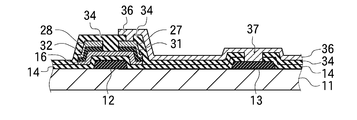
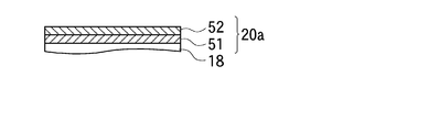
- Diagram for explaining the transistor manufacturing method of the present invention Diagram for explaining the transistor manufacturing method of the present invention : Diagram for explaining the transistor manufacturing method of the present invention : Diagram for explaining the transistor manufacturing method of the present invention : Diagram for explaining the transistor manufacturing method of the present invention : Diagram for explaining the transistor manufacturing method of the present invention : Diagram for explaining the transistor manufacturing method of the present invention : Diagram for explaining the transistor manufacturing method of the present invention : Diagram for explaining the transistor manufacturing method of the present invention : Diagram for explaining the transistor manufacturing method of the present invention Diagram for explaining metal wiring film The figure for demonstrating the film-forming apparatus which manufactures the transistor of this invention Graph for comparing the specific resistance of the adhesion layer using O 2 gas and the adhesion layer using CO 2 gas
- Transistor 10 Processing object 12... Gate electrode 14... Gate insulating layer 16... Silicon layer 18... N-type silicon layer 20 a, 20 b. Drain electrode film 31... Source region 32... Drain region 51... Adhesion layer 52... Metal low resistance layer 111... Copper alloy target 112.
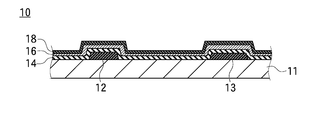
- Reference numeral 10 in FIG. 1A indicates an object to be processed in which the transistor manufacturing method of the present invention is used.
- the processing object 10 will be described.
- the processing object 10 has a transparent substrate 11 made of glass or the like, and the gate electrode 12 and the pixel electrode 13 are arranged on the transparent substrate 11 so as to be separated from each other. .
- a gate insulating layer 14, a silicon layer 16, and an n-type silicon layer 18 are arranged in this order from the transparent substrate 11 side so as to cover the gate electrode 12 and the pixel electrode 13.
- the n-type silicon layer 18 is a silicon layer having a resistance value lower than that of the silicon layer 16 by addition of impurities.
- the n-type silicon layer 18 and the silicon layer 16 are made of amorphous silicon, but may be monocrystalline or polycrystalline.
- the gate insulating layer 14 is an insulating film such as a silicon nitride thin film, and may be a silicon oxynitride film or another insulating film.
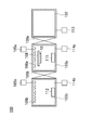
- Reference numeral 100 in FIG. 3 indicates a film forming apparatus that forms a metal wiring film on the surface of the processing object 10.
- the film forming apparatus 100 includes a carry-in / out chamber 102, a first film forming chamber 103a, and a second film forming chamber 103b.
- the carry-in / out chamber 102 and the first film forming chamber 103a and the first film forming chamber 103a and the second film forming chamber 103b are connected to each other through gate valves 109a and 109b, respectively.
- the evacuation systems 113, 114a, 114b are connected to the carry-in / out chamber 102 and the first and second film forming chambers 103a, 103b, respectively, and the gate valves 109a, 109b are closed, and the first and second components are formed.
- the inside of the film chambers 103a and 103b is evacuated.
- the door between the loading / unloading chamber 102 and the atmosphere is opened, the processing object 10 is loaded into the loading / unloading chamber 102, the door is closed, the inside of the loading / unloading chamber 102 is evacuated, the gate valve 109 a is opened, and the processing is performed.
- the object 10 is moved into the first film formation chamber 103a and held by the substrate holder 108.
- a copper alloy target 111 and a pure copper target 112 are respectively arranged on the bottom wall side inside the first and second film forming chambers 103a, and the n-type silicon layer 18 of the object to be processed 10 is the target 111. , 112 are held by the substrate holder 108 so that they can face each other.
- Gas introduction systems 105a and 105b are connected to the first and second film formation chambers 103a and 103b, respectively, and the gas introduction system 105a oxidizes the sputtering gas and the oxidation gas while evacuating the inside of the first film formation chamber 103a.
- the gas introduction system 105a oxidizes the sputtering gas and the oxidation gas while evacuating the inside of the first film formation chamber 103a.
- the sputtered particles made of the constituent material of the copper alloy target 111 reach the surface of the n-type silicon layer 18 and an adhesion layer in contact with the n-type silicon layer 18 is formed.
- the copper alloy target 111 contains an additive metal consisting of at least one of Ti (titanium), Zr (zirconium), and Cr (chromium) and copper, and the number of atoms of copper and the additive metal is 100 atomic%. When added, the added metal is contained in a proportion of 5 atomic% to 30 atomic%.
- the oxidizing gas is a gas that oxidizes the added metal and generates an oxide of the added metal.
- the surface of the film formation target 10 has copper as a main component, and the added metal. An adhesion layer containing the oxide is formed.
- a sputtering gas is introduced from the gas introduction system 105b, and the pure copper target 112 is sputtered, the surface of the processing object 10 is obtained.
- sputtered particles made of copper atoms, which are constituent materials of the pure copper target 112 arrive, and a metal low resistance layer made of pure copper is formed on the surface of the adhesion layer.
- no oxidizing gas is introduced in the second film formation chamber 103b.
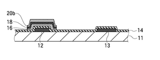
- Reference numeral 20a in FIG. 1B indicates a metal wiring film composed of an adhesion layer and a low resistance layer
- reference numerals 51 and 52 in FIG. 2 indicate an adhesion layer and a metal low resistance layer, respectively.
- a resist film is disposed on the surface of the portion of the metal wiring film 20a located on the gate electrode 12, and the laminated film composed of the metal wiring film 20a, the n-type silicon layer 18 and the silicon layer 16 is etched, and the laminated film The portion not covered with the resist film is removed.
- FIG. 1C shows a state in which the resist film has been removed after etching the laminated film
- reference numeral 20b represents the metal wiring film remaining after being covered with the resist film.
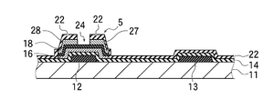
- a patterned resist film 22 is disposed on the metal wiring film 20b, and the surface of the metal wiring film 20b is exposed on the bottom surface of the opening 24 of the resist film 22.
- an etching solution such as a mixed solution of phosphoric acid / nitric acid / acetic acid, a mixed solution of sulfuric acid / nitric acid / acetic acid, or a ferric chloride solution
- the exposed portion of the metal wiring film 20b is etched, and the metal wiring film 20b Is patterned.
- an opening 24 through which the n-type silicon layer 18 is exposed is formed on the bottom surface of the metal wiring film 20b on the gate electrode 12, and the metal wiring film 20b is separated by the opening 24, as shown in FIG.
- the source electrode film 27 and the drain electrode film 28 are formed, and the transistor 5 of the present invention is obtained.
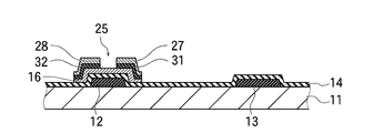
- the n-type silicon layer 18 that is carried into the etching apparatus and exposed at the bottom surface of the opening 24 is etched by being exposed to plasma of an etching gas, so that the silicon layer 16 is exposed at the bottom surface of the opening 24 formed in the n-type silicon layer 18.
- the opening 24 formed in the n-type silicon layer 18 is located above the gate electrode 12, and the n-type silicon layer 18 is separated into the source region 31 and the drain region 32 by the opening 24.
- the surface of the silicon layer 16 is exposed at the bottom surface of the opening 25, and when the silicon layer 16 is exposed to etching gas plasma when etching the n-type silicon layer 18, hydrogen atoms are lost from the surface of the silicon layer 16. As a result, dangling bonds are formed.
- This dangling bond causes TFT characteristic defects such as leakage current.
- hydrogen is introduced to generate hydrogen plasma with the source electrode film 27 and the drain electrode film 28 exposed, When the silicon layer 16 exposed at the bottom of the opening 25 is exposed to hydrogen gas plasma, silicon atoms on the surface of the silicon layer 16 are combined with hydrogen and dangling bonds disappear.
- the source electrode film 27 and the drain electrode film 28 include the adhesion layer 51 containing copper as a main component and containing an additive metal at a ratio of 5 atomic% to 30 atomic%. Even if the source electrode film 27 and the drain electrode film 28 are exposed to hydrogen plasma, the n-type silicon layer 18 (the source region 31 and the drain layer) is formed. Copper does not precipitate at the interface with the region 32), and the electrode film composed of the metal wiring film 20a (20b) such as the source electrode film 27 and the drain electrode film 28 does not peel off.
- a passivation film 34 is formed as shown in FIG. 1 (h), a contact hole 37 is formed in the passivation film 34, and then a source electrode is formed as shown in FIG. 1 (i).
- a transparent electrode film 36 that connects the film 27 or the drain electrode film 28 and the pixel electrode 13 or the like is formed, a liquid crystal display panel is obtained.
- Gases that can be used for etching a silicon layer are Cl 2 , HBr, Cl 2 , HCl, CBrF 3 , SiCl 4 , BCl 3 , CHF 3 , PCl 3 , HI. , I 2 etc.
- One of these halogen gases may be used alone as an etching gas, or two or more of these halogen gases may be mixed and used as an etching gas.
- an additive gas other than a halogen gas such as O 2 , N 2 , SF 6 , N 2 , Ar, NH 3 may be added to the etching gas.
- the halogen gas can also be used when etching other etching objects such as silicon nitride (SiN), silicon oxide (SiO 2 ) GaAs, SnO 2 , Cr, Ti, TiN, W, and Al. is there.
- Examples of polysilicon etching gas include Cl 2 , Cl 2 + HBr, Cl 2 + O 2 , CF 4 + O 2 , SF 6 , Cl 2 + N 2 , Cl 2 + HCl, HBr + Cl 2 + SF 6, and the like.
- Examples of the etching gas for Si include SF 6 , C 4 F 8 , CBrF 3 , CF 4 + O 2 , Cl 2 , SiCl 4 + Cl 2 , SF 6 + N 2 + Ar, BCl 2 + Cl 2 + Ar, CF 4 , NF 3 , SiF 4 , BF 3 , XeF 2 , ClF 3 , SiCl 4 , PCl 3 , BCl 3 , HCl, HBr, Br 2 , HI, I 2, etc.
- Examples of the etching gas for amorphous silicon include CF 4 + O 2 and Cl 2 + SF 6 .
- the adhesion layer 51 is formed of 100% additive metal (metal Ti film, metal Zr film, etc.) and a pure copper metal low resistance layer 52 is laminated on the surface to form a metal wiring film, the metal low resistance made of pure copper
- the layer 52 and the metal low resistance layer 52 mainly composed of copper are etched using a mixed solution of phosphoric acid / nitric acid / acetic acid, a mixed solution of sulfuric acid / nitric acid / acetic acid, or a ferric chloride solution as an etchant.
- the adhesion layer 51 made of 100% additive metal or the adhesion layer 51 containing a large amount of additive metal has a significantly different etching rate from the pure copper metal low-resistance layer 52, and the metal low-resistance layer 52 and the adhesion layer. 51.
- the pure Ti thin film and the pure Zr thin film are insoluble in the etchant of the pure copper metal low resistance layer 52 and are soluble in the hydrofluoric acid strong acid etching solution. Such etchant is To dissolve the scan or Si, can not be used for TFT.).
- the adhesion layer 51 of 100% added metal is used as a barrier layer for the silicon layer and a copper thin film is formed on the surface, first, the copper thin film is patterned using an etching solution such as phosphoric acid / nitric acid / acetic acid mixed solution. Then, after exposing the barrier film surface, it is necessary to execute a dry etching process using an etching gas. Therefore, the number of processes increases and the cost increases.
- an etching solution such as phosphoric acid / nitric acid / acetic acid mixed solution.
- the adhesion layer 51 contains more copper than the additive metal
- the adhesion layer 51 and the metal low resistance layer 52 can be wet-etched with the same etching solution. Further, the adhesion layer 51 and the metal low-resistance layer 52 can be etched using the same resist film without re-arranging the resist film, so that the cost is low.
- the hydrogen gas flow rate is 500 sccm
- the pressure is 200 Pa
- the substrate temperature is 250 ° C.
- the power is 300 W
- the time is 60 seconds.
- the silicon nitride film was formed at a pressure of 120 Pa, a substrate temperature of 250 ° C., and a power of 300 W by introducing each gas at a ratio of SiH 4 : 20 sccm, NH 3 gas 300 sccm, and N 2 gas 500 sccm in a CVD apparatus in which the substrate was placed. .
- Adhesion of metal wiring film before exposure to hydrogen plasma (as depo. Adhesion) and adhesion after formation of silicon nitride film on the surface after exposure to hydrogen plasma (adhesion after H 2 plasma treatment) ) was measured by a tape test in which the adhesive tape was adhered and then peeled off, and the glass substrate surface exposed was evaluated as “x”, and the others were evaluated as “ ⁇ ”.
- the experiment was performed by changing the content ratio of the additive metal and the introduction ratio of the oxidizing gas.
- the evaluation results are shown in Tables 1 to 3 below as “adhesiveness”. Also, after forming the same metal wiring film on the surface of the silicon wafer as described above, annealing is performed in a vacuum atmosphere, and after removing the metal wiring film by etching, the surface is observed with an SEM to diffuse copper into silicon. The presence or absence of was observed.
- the sputtering gas is argon gas
- the oxidizing gas is oxygen gas
- the sputtering gas partial pressure in the sputtering atmosphere is 0.4 Pa.
- oxygen gas instead of oxygen gas, a target containing an added metal was sputtered using CO 2 gas as an oxidizing gas.
- Ar gas was used as a sputtering gas
- Ti was used as an additive metal
- adhesion and barrier properties were evaluated.
- the sputtering gas partial pressure is the same as above.
- the adhesion adheresion before and after the H 2 plasma treatment
- barrier properties are good when the additive metal is contained at 5 atomic% or more.
- the oxidizing gas may be introduced in a range of 3 parts by volume or more and 15 parts by volume or less with respect to 100 parts by volume of the argon gas.
- FIG. 4 shows the specific resistance of an adhesion layer (corresponding to the adhesion layer in the experimental results in Table 1) obtained when sputtering a copper alloy target 111 containing 10 atomic% Ti as an additive metal with Ar gas and O 2 gas.
- 5 is a graph showing the specific resistance of an adhesion layer (corresponding to the adhesion layer in the experimental results of Table 4) obtained when sputtering with Ar gas CO 2 gas. While towards CO 2 gas specific resistance in a range wider than O 2 gas is small, it is considered towards the CO 2 gas is due to the low oxidizing power than O 2 gas.
- the adhesion layer 51 preferably has high adhesion to the metal low resistance layer 52 in addition to adhesion to silicon or silicon oxide, the adhesion layer 51 of the present invention is a component of the metal low resistance layer 52. Contains 50% or more of copper.
Landscapes
- Chemical & Material Sciences (AREA)
- Chemical Kinetics & Catalysis (AREA)
- Engineering & Computer Science (AREA)
- Materials Engineering (AREA)
- Mechanical Engineering (AREA)
- Metallurgy (AREA)
- Organic Chemistry (AREA)
- Inorganic Chemistry (AREA)
- Electrodes Of Semiconductors (AREA)
- Thin Film Transistor (AREA)
- Internal Circuitry In Semiconductor Integrated Circuit Devices (AREA)
- Physical Vapour Deposition (AREA)
Abstract
Priority Applications (3)
| Application Number | Priority Date | Filing Date | Title |
|---|---|---|---|
| CN2009801090943A CN101971350B (zh) | 2008-04-15 | 2009-04-08 | 薄膜晶体管、薄膜晶体管的制造方法 |
| JP2010508180A JP5282085B2 (ja) | 2008-04-15 | 2009-04-08 | 薄膜トランジスタ、薄膜トランジスタの製造方法 |
| US12/881,641 US20110068402A1 (en) | 2008-04-15 | 2010-09-14 | Thin film transistor and method for producing thin film transistor |
Applications Claiming Priority (2)
| Application Number | Priority Date | Filing Date | Title |
|---|---|---|---|
| JP2008-106119 | 2008-04-15 | ||
| JP2008106119 | 2008-04-15 |
Related Child Applications (1)
| Application Number | Title | Priority Date | Filing Date |
|---|---|---|---|
| US12/881,641 Continuation US20110068402A1 (en) | 2008-04-15 | 2010-09-14 | Thin film transistor and method for producing thin film transistor |
Publications (1)
| Publication Number | Publication Date |
|---|---|
| WO2009128372A1 true WO2009128372A1 (fr) | 2009-10-22 |
Family
ID=41199069
Family Applications (1)
| Application Number | Title | Priority Date | Filing Date |
|---|---|---|---|
| PCT/JP2009/057176 Ceased WO2009128372A1 (fr) | 2008-04-15 | 2009-04-08 | Transistor à couche mince et procédé de fabrication associé |
Country Status (6)
| Country | Link |
|---|---|
| US (1) | US20110068402A1 (fr) |
| JP (1) | JP5282085B2 (fr) |
| KR (1) | KR101098206B1 (fr) |
| CN (1) | CN101971350B (fr) |
| TW (1) | TW201001499A (fr) |
| WO (1) | WO2009128372A1 (fr) |
Cited By (5)
| Publication number | Priority date | Publication date | Assignee | Title |
|---|---|---|---|---|
| JP2010287791A (ja) * | 2009-06-12 | 2010-12-24 | Mitsubishi Materials Corp | 配線層構造及びその製造方法 |
| US20110291234A1 (en) * | 2010-05-27 | 2011-12-01 | Sang-Yun Lee | Semiconductor circuit structure and method of making the same |
| WO2013157468A1 (fr) * | 2012-04-18 | 2013-10-24 | 山陽特殊製鋼株式会社 | ALLIAGE À BASE DE CrTi POUR UNE COUCHE DE FILM D'ADHÉRENCE DESTINÉE À UN SUPPORT D'ENREGISTREMENT MAGNÉTIQUE, MATÉRIAU CIBLE DE PULVÉRISATION, ET SUPPORT D'ENREGISTREMENT MAGNÉTIQUE PERPENDICULAIRE OBTENU AU MOYEN DUDIT ALLIAGE |
| JP2016009186A (ja) * | 2014-06-23 | 2016-01-18 | 上海和輝光電有限公司Everdisplay Optronics (Shanghai) Limited | 有機発光ディスプレイ装置及びその薄膜トランジスタ |
| WO2019093348A1 (fr) * | 2017-11-09 | 2019-05-16 | 三井金属鉱業株式会社 | Structure de câblage et matériau cible |
Families Citing this family (3)
| Publication number | Priority date | Publication date | Assignee | Title |
|---|---|---|---|---|
| JP5247448B2 (ja) * | 2006-08-10 | 2013-07-24 | 株式会社アルバック | 導電膜形成方法、薄膜トランジスタの製造方法 |
| JP5659966B2 (ja) * | 2010-06-29 | 2015-01-28 | 日亜化学工業株式会社 | 半導体素子及びその製造方法 |
| CN103295970B (zh) * | 2013-06-05 | 2015-04-29 | 京东方科技集团股份有限公司 | 阵列基板、其制造方法及显示装置 |
Citations (3)
| Publication number | Priority date | Publication date | Assignee | Title |
|---|---|---|---|---|
| JPH04192527A (ja) * | 1990-11-27 | 1992-07-10 | Toshiba Corp | 半導体装置 |
| JPH04302436A (ja) * | 1991-03-29 | 1992-10-26 | Casio Comput Co Ltd | 薄膜半導体素子及びその製造方法 |
| JP2006041128A (ja) * | 2004-07-26 | 2006-02-09 | Kobe Steel Ltd | 半導体装置のCu系配線形成方法 |
Family Cites Families (7)
| Publication number | Priority date | Publication date | Assignee | Title |
|---|---|---|---|---|
| JPH06252146A (ja) | 1993-02-23 | 1994-09-09 | Seiko Epson Corp | 半導体装置 |
| JPH0992649A (ja) | 1995-07-17 | 1997-04-04 | Nippon Telegr & Teleph Corp <Ntt> | 半導体装置の配線構造およびその製造方法 |
| EP1155816B1 (fr) * | 1998-12-28 | 2007-02-14 | Asahi Glass Company Ltd. | Produit en couches |
| KR100947525B1 (ko) * | 2003-03-12 | 2010-03-12 | 삼성전자주식회사 | 액정 표시 장치용 박막 트랜지스터 기판 및 이의 제조방법 |
| TW200805667A (en) * | 2006-07-07 | 2008-01-16 | Au Optronics Corp | A display panel structure having a circuit element and a method of manufacture |
| JP5247448B2 (ja) * | 2006-08-10 | 2013-07-24 | 株式会社アルバック | 導電膜形成方法、薄膜トランジスタの製造方法 |
| US7919795B2 (en) * | 2006-12-21 | 2011-04-05 | Samsung Electronics Co., Ltd. | Wire structure, method for fabricating wire, thin film transistor substrate, and method for fabricating the thin film transistor substrate |
-
2009
- 2009-04-08 WO PCT/JP2009/057176 patent/WO2009128372A1/fr not_active Ceased
- 2009-04-08 CN CN2009801090943A patent/CN101971350B/zh active Active
- 2009-04-08 KR KR1020107019937A patent/KR101098206B1/ko not_active Expired - Fee Related
- 2009-04-08 JP JP2010508180A patent/JP5282085B2/ja active Active
- 2009-04-14 TW TW098112327A patent/TW201001499A/zh unknown
-
2010
- 2010-09-14 US US12/881,641 patent/US20110068402A1/en not_active Abandoned
Patent Citations (3)
| Publication number | Priority date | Publication date | Assignee | Title |
|---|---|---|---|---|
| JPH04192527A (ja) * | 1990-11-27 | 1992-07-10 | Toshiba Corp | 半導体装置 |
| JPH04302436A (ja) * | 1991-03-29 | 1992-10-26 | Casio Comput Co Ltd | 薄膜半導体素子及びその製造方法 |
| JP2006041128A (ja) * | 2004-07-26 | 2006-02-09 | Kobe Steel Ltd | 半導体装置のCu系配線形成方法 |
Cited By (9)
| Publication number | Priority date | Publication date | Assignee | Title |
|---|---|---|---|---|
| JP2010287791A (ja) * | 2009-06-12 | 2010-12-24 | Mitsubishi Materials Corp | 配線層構造及びその製造方法 |
| US20120068265A1 (en) * | 2009-06-12 | 2012-03-22 | Ulvac, Inc. | Wiring layer structure and process for manufacture thereof |
| US8624397B2 (en) * | 2009-06-12 | 2014-01-07 | Mitsubishi Materials Corporation | Electrode layer structure for a thin-film transistor and process for manufacture thereof |
| US20110291234A1 (en) * | 2010-05-27 | 2011-12-01 | Sang-Yun Lee | Semiconductor circuit structure and method of making the same |
| US8455978B2 (en) * | 2010-05-27 | 2013-06-04 | Sang-Yun Lee | Semiconductor circuit structure and method of making the same |
| WO2013157468A1 (fr) * | 2012-04-18 | 2013-10-24 | 山陽特殊製鋼株式会社 | ALLIAGE À BASE DE CrTi POUR UNE COUCHE DE FILM D'ADHÉRENCE DESTINÉE À UN SUPPORT D'ENREGISTREMENT MAGNÉTIQUE, MATÉRIAU CIBLE DE PULVÉRISATION, ET SUPPORT D'ENREGISTREMENT MAGNÉTIQUE PERPENDICULAIRE OBTENU AU MOYEN DUDIT ALLIAGE |
| JP2013222488A (ja) * | 2012-04-18 | 2013-10-28 | Sanyo Special Steel Co Ltd | 磁気記録媒体に用いる密着膜層用CrTi系合金およびスパッタリング用ターゲット材並びにそれを使用した垂直磁気記録媒体 |
| JP2016009186A (ja) * | 2014-06-23 | 2016-01-18 | 上海和輝光電有限公司Everdisplay Optronics (Shanghai) Limited | 有機発光ディスプレイ装置及びその薄膜トランジスタ |
| WO2019093348A1 (fr) * | 2017-11-09 | 2019-05-16 | 三井金属鉱業株式会社 | Structure de câblage et matériau cible |
Also Published As
| Publication number | Publication date |
|---|---|
| JPWO2009128372A1 (ja) | 2011-08-04 |
| KR101098206B1 (ko) | 2011-12-23 |
| KR20100110388A (ko) | 2010-10-12 |
| US20110068402A1 (en) | 2011-03-24 |
| CN101971350B (zh) | 2012-10-10 |
| JP5282085B2 (ja) | 2013-09-04 |
| CN101971350A (zh) | 2011-02-09 |
| TW201001499A (en) | 2010-01-01 |
Similar Documents
| Publication | Publication Date | Title |
|---|---|---|
| JP5282086B2 (ja) | 薄膜トランジスタの製造方法、薄膜トランジスタ | |
| JP5285710B2 (ja) | 薄膜トランジスタの製造方法 | |
| JP5282085B2 (ja) | 薄膜トランジスタ、薄膜トランジスタの製造方法 | |
| TWI572745B (zh) | 用於含銅金屬薄膜之蝕刻劑組成物以及使用其之蝕刻方法 | |
| JP6077978B2 (ja) | 薄膜トランジスタおよびその製造方法 | |
| WO2014104296A1 (fr) | Transistor en couches minces et son procédé de fabrication | |
| CN102804352B (zh) | 布线层结构及其制造方法 | |
| CN110867458A (zh) | 金属氧化物半导体薄膜晶体管阵列基板及制作方法 | |
| JPH06283481A (ja) | 酸化スズインジウムの反応性イオンエッチング方法 | |
| JP2012189726A (ja) | Ti合金バリアメタルを用いた配線膜および電極、並びにTi合金スパッタリングターゲット | |
| US7012029B2 (en) | Method of forming a lamination film pattern and improved lamination film pattern | |
| JP2012189725A (ja) | Ti合金バリアメタルを用いた配線膜および電極、並びにTi合金スパッタリングターゲット | |
| JP5424876B2 (ja) | 薄膜トランジスタ製造方法、液晶表示装置製造方法、電極形成方法 | |
| Yu et al. | The properties of Cu metallization based on CuMgAl alloy buffer layer | |
| JP2012015200A (ja) | 薄膜トランジスタ基板、および薄膜トランジスタ基板を備えた表示デバイス | |
| JPWO2010143609A1 (ja) | 電子装置の形成方法、電子装置、半導体装置及びトランジスタ | |
| TW201030819A (en) | Al alloy film for display device, thin film transistor substrate, method for manufacturing same, and display device |
Legal Events
| Date | Code | Title | Description |
|---|---|---|---|
| WWE | Wipo information: entry into national phase |
Ref document number: 200980109094.3 Country of ref document: CN |
|
| 121 | Ep: the epo has been informed by wipo that ep was designated in this application |
Ref document number: 09732696 Country of ref document: EP Kind code of ref document: A1 |
|
| ENP | Entry into the national phase |
Ref document number: 20107019937 Country of ref document: KR Kind code of ref document: A |
|
| WWE | Wipo information: entry into national phase |
Ref document number: 2010508180 Country of ref document: JP |
|
| NENP | Non-entry into the national phase |
Ref country code: DE |
|
| 122 | Ep: pct application non-entry in european phase |
Ref document number: 09732696 Country of ref document: EP Kind code of ref document: A1 |