WO2009133799A1 - 固体撮像装置 - Google Patents
固体撮像装置 Download PDFInfo
- Publication number
- WO2009133799A1 WO2009133799A1 PCT/JP2009/058007 JP2009058007W WO2009133799A1 WO 2009133799 A1 WO2009133799 A1 WO 2009133799A1 JP 2009058007 W JP2009058007 W JP 2009058007W WO 2009133799 A1 WO2009133799 A1 WO 2009133799A1
- Authority
- WO
- WIPO (PCT)
- Prior art keywords
- charge
- photoelectric conversion
- transfer
- type semiconductor
- semiconductor layer
- Prior art date
- Legal status (The legal status is an assumption and is not a legal conclusion. Google has not performed a legal analysis and makes no representation as to the accuracy of the status listed.)
- Ceased
Links
Images




Classifications
-
- H—ELECTRICITY
- H10—SEMICONDUCTOR DEVICES; ELECTRIC SOLID-STATE DEVICES NOT OTHERWISE PROVIDED FOR
- H10F—INORGANIC SEMICONDUCTOR DEVICES SENSITIVE TO INFRARED RADIATION, LIGHT, ELECTROMAGNETIC RADIATION OF SHORTER WAVELENGTH OR CORPUSCULAR RADIATION
- H10F39/00—Integrated devices, or assemblies of multiple devices, comprising at least one element covered by group H10F30/00, e.g. radiation detectors comprising photodiode arrays
- H10F39/10—Integrated devices
- H10F39/12—Image sensors
- H10F39/15—Charge-coupled device [CCD] image sensors
- H10F39/153—Two-dimensional or three-dimensional array CCD image sensors
-
- H—ELECTRICITY
- H04—ELECTRIC COMMUNICATION TECHNIQUE
- H04N—PICTORIAL COMMUNICATION, e.g. TELEVISION
- H04N25/00—Circuitry of solid-state image sensors [SSIS]; Control thereof
- H04N25/70—SSIS architectures; Circuits associated therewith
- H04N25/71—Charge-coupled device [CCD] sensors; Charge-transfer registers specially adapted for CCD sensors
- H04N25/713—Transfer or readout registers; Split readout registers or multiple readout registers
-
- H—ELECTRICITY
- H10—SEMICONDUCTOR DEVICES; ELECTRIC SOLID-STATE DEVICES NOT OTHERWISE PROVIDED FOR
- H10F—INORGANIC SEMICONDUCTOR DEVICES SENSITIVE TO INFRARED RADIATION, LIGHT, ELECTROMAGNETIC RADIATION OF SHORTER WAVELENGTH OR CORPUSCULAR RADIATION
- H10F39/00—Integrated devices, or assemblies of multiple devices, comprising at least one element covered by group H10F30/00, e.g. radiation detectors comprising photodiode arrays
- H10F39/10—Integrated devices
- H10F39/12—Image sensors
- H10F39/15—Charge-coupled device [CCD] image sensors
- H10F39/152—One-dimensional array CCD image sensors
Definitions
- the present invention relates to a solid-state imaging device.
- a solid-state imaging device As a solid-state imaging device, a plurality of photoelectric conversion units each having a light-sensitive region that has a substantially rectangular shape that generates charges in response to light incidence and has a planar shape formed by two long sides and two short sides Those arranged in an array in the original direction (the direction along the short side direction of the photosensitive region) are known (see, for example, Patent Document 1). Such a solid-state imaging device has been conventionally used for various applications, and in particular, is widely used as a light detection means of a spectroscope. JP 2005-164363 A
- the solid-state imaging device described in Patent Document 1 has the following problems.
- charges generated in the photosensitive region are read from the short side of the photosensitive region. For this reason, the generated charges need to move in the long side direction of the photosensitive region, and the moving distance becomes long. As a result, it is difficult to read out the generated charges at high speed.
- a diffusion region for accumulating charges and an amplifier region for amplifying and outputting a voltage signal generated in the diffusion region are disposed adjacent to each of the pair of short sides of the photosensitive region.
- signals are output from a pair of amplifier regions arranged adjacent to each short side of the photosensitive region, signal processing for obtaining a one-dimensional image is performed. This is necessary and the image processing may be complicated.
- an object of the present invention is to provide a solid-state imaging device capable of reading out charges generated in a photosensitive region at high speed without complicating image processing.
- the solid-state imaging device generates a charge in response to light incidence and has a light-sensitive region having a substantially rectangular shape whose planar shape is formed by two long sides and two short sides, and a light-sensitive region. And a potential gradient forming region for forming a potential gradient that is increased along a predetermined direction parallel to the long side forming the planar shape of the photosensitive region, and so as to be along a direction intersecting the predetermined direction.
- the potential gradient formed along the predetermined direction is formed by the potential gradient formation region, so that the charge generated in the photosensitive region is formed. It moves to one of the short sides along the potential gradient due to the potential gradient. As a result, the charge transfer speed is governed by the potential gradient (potential gradient), and the charge read speed is increased.
- the charges transferred from the plurality of photoelectric conversion units are acquired by the first or second charge output unit, transferred in the above-described direction crossing a predetermined direction, and output.
- the photosensitive region has a substantially rectangular shape whose planar shape is formed by two long sides and two short sides. For this reason, the saturation charge amount in the photosensitive region is large.
- the potential gradient forming region forms, as the predetermined direction, a potential gradient which is increased along a first direction from one short side to the other short side forming the planar shape of the photosensitive region.
- the first and second charge output units are arranged on the other short side forming the planar shape of the photosensitive region, and correspond to the photoelectric conversion units, respectively, and each photoelectric conversion unit and the first charge output.
- a plurality of first transfer units that are arranged between the first and second photoelectric transfer units and transfer the charges from the photosensitive region of the corresponding photoelectric conversion unit to the first charge output unit, and each of the first transfer units corresponds to the photoelectric conversion unit and A plurality of second transfer units that are arranged between the charge output unit and the second charge output unit and transfer the charges transferred to the first charge output unit to the second charge output unit; I have.
- the charge generated in the photosensitive region is transferred to the other short side along the potential gradient due to the formed potential gradient. Move to.
- the electric charge that has moved to the other short side is acquired by the first transfer unit and transferred in the first direction.
- the charges transferred from each first transfer unit are transferred and output in a direction crossing the first direction by the first charge output unit.
- the charges accumulated in the first charge output unit are transferred in the first direction by the second transfer unit.
- the charges transferred from each second transfer unit are transferred and output in a direction crossing the first direction by the second charge output unit.
- the potential gradient forming region has, as the predetermined direction, a first direction from one short side forming the planar shape of the photosensitive region to the other short side and the other forming the planar shape of the photosensitive region.
- the potential gradient raised along any one of the second directions from the short side to the one short side is selectively formed, and the first charge output portion has a planar shape of the photosensitive region.
- the second charge output unit is arranged on the other short side forming the planar shape of the photosensitive region, and corresponds to each photoelectric conversion unit and each photoelectric conversion unit And a plurality of first transfer units that are arranged between the first charge output unit and transfer charges from the photosensitive region of the corresponding photoelectric conversion unit to the first charge output unit, respectively, Corresponding and arranged between each photoelectric conversion unit and the second charge output unit, the corresponding light Further comprises a plurality of second transfer unit for transferring the charges from the photosensitive region of the conversion unit to the second charge output portion.
- the second charge output unit acquires the charges generated in the photoelectric conversion unit over the first period from the plurality of second transfer units, and transfers and outputs the charges in a direction crossing a predetermined direction.
- the first charge output unit acquires charges generated in the photoelectric conversion unit over a second period shorter than the first period from the plurality of first transfer units, and intersects with a predetermined direction. Transfer and output.
- the exposure time becomes relatively long, so that strong incident light is difficult to detect properly because the signal is saturated, but weak. Incident light is detected as a sufficiently large signal. If the charge generated in the photoelectric conversion unit is accumulated over the second period, the exposure time becomes relatively short. Therefore, weak incident light has a weak signal, and it is difficult to detect it sufficiently as a signal. However, strong incident light is appropriately detected as a signal without saturation. Thus, regardless of the intensity of the incident light, the incident light is appropriately detected as a signal, and the effective dynamic range is increased.
- the transfer of charges generated in the photoelectric conversion unit over the second period and the charge generated in the photoelectric conversion unit over the first period are performed. Transfer does not interfere with each other.
- FIG. 1 is a diagram illustrating a configuration of the solid-state imaging device according to the first embodiment.
- FIG. 2 is a view for explaining a cross-sectional configuration along the line II-II in FIG.
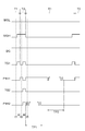
- FIG. 3 is a timing chart of each input signal in the solid-state imaging device according to the first embodiment.
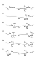
- FIG. 4 is a potential diagram for explaining the charge accumulation and discharge operations at each time in FIG.
- FIG. 5 is a schematic diagram for explaining charge movement in the photoelectric conversion unit.
- FIG. 6 is a diagram illustrating a configuration of the solid-state imaging device according to the second embodiment.
- FIG. 7 is a view for explaining a cross-sectional configuration along the line VII-VII in FIG.
- FIG. 8 is a timing chart of each input signal in the solid-state imaging device according to the second embodiment.
- FIG. 9 is a potential diagram for explaining the charge accumulation and discharge operation at each time in FIG.
- DESCRIPTION OF SYMBOLS 1 ... Solid-state imaging device, 3 ... Photoelectric conversion part, 5 ... Buffer gate part, 7 ... 1st transfer part, 9 ... 1st shift register, 11 ... 2nd transfer part, 13 ... 2nd shift register, DESCRIPTION OF SYMBOLS 15 ... Photosensitive area
- FIG. 1 is a diagram illustrating a configuration of the solid-state imaging device according to the first embodiment.
- FIG. 2 is a view for explaining a cross-sectional configuration along the line II-II in FIG.
- the solid-state imaging device 1 includes a plurality of photoelectric conversion units 3, a plurality of buffer gate units 5, a plurality of first transfer units 7, and a first shift as a first charge output unit.
- a register 9, a plurality of second transfer units 11, and a second shift register 13 as a second charge output unit are provided.
- the solid-state imaging device 1 can be used as light detection means for a spectroscope.
- Each photoelectric conversion unit 3 has a photosensitive region 15 and a potential gradient forming region 17.
- the light sensitive region 15 generates a charge corresponding to the incident light intensity in response to light incidence.
- the potential gradient forming region 17 has a first direction (the long side direction of the photosensitive region 15) from one short side forming the planar shape of the photosensitive region 15 toward the other short side with respect to the photosensitive region 15. The potential gradient is increased along the direction of The electric charge generated in the photosensitive region 15 by the potential gradient forming region 17 is discharged from the other short side of the photosensitive region 15.
- the planar shape of the photosensitive region 15 is a substantially rectangular shape formed by two long sides and two short sides.
- the plurality of photoelectric conversion units 3 are juxtaposed along a direction intersecting (for example, orthogonal to) the first direction and arranged in an array in a one-dimensional direction.
- the plurality of photoelectric conversion units 3 are juxtaposed in the direction along the short side direction of the photosensitive region 15.
- the length of the photosensitive region 15 in the long side direction is set to about 1 mm, for example, and the length of the photosensitive region 15 in the short side direction is set to about 24 ⁇ m, for example.
- an isolation region 18 and an overflow drain (OFD) region 19 are arranged so as to sandwich the photosensitive region 15 in a direction along the short side direction of the photosensitive region 15.
- the isolation region 18 is adjacent to one long side of the photosensitive region 15 and extends in a direction along the long side direction of the photosensitive region 15.
- the isolation region 18 electrically isolates a pair of adjacent photosensitive regions 15 with the isolation region 18 in between.
- the overflow drain region 19 is adjacent to the other long side of the photosensitive region 15 and extends in a direction along the long side direction of the photosensitive region 15.
- the overflow drain region 19 includes an overflow gate (OFG) composed of a gate transistor, and when charge exceeding the storage capacity of the light sensitive region 15 is generated in the light sensitive region 15, the amount exceeding the storage capacity Discharge charge. Thereby, inconveniences such as blooming in which the charges overflowing from the photosensitive region 15 exceeding the storage capacity leak to the other photosensitive regions 15 are prevented.
- OFG overflow gate
- Each buffer gate portion 5 corresponds to the photoelectric conversion portion 3 and is disposed on the other short side forming the planar shape of the photosensitive region 15. That is, the plurality of buffer gate portions 5 are juxtaposed in the direction intersecting the first direction (the direction along the short side direction of the photosensitive region 15) on the other short side forming the planar shape of the photosensitive region 15. Has been.
- the buffer gate unit 5 partitions the photoelectric conversion unit 3 (photosensitive region 15) and the first transfer unit 7 from each other. In the present embodiment, the charge discharged from the photosensitive region 15 by the potential gradient forming region 17 is accumulated in the buffer gate portion 5.
- An isolation region (not shown) is disposed between the adjacent buffer gate portions 5 to achieve electrical isolation between the buffer gate portions 5.
- Each first transfer unit 7 corresponds to the buffer gate unit 5 and is disposed between the buffer gate unit 5 and the first shift register 9. That is, the plurality of first transfer units 7 are juxtaposed on the other short side forming the planar shape of the photosensitive region 15 in a direction crossing the first direction.
- the first transfer unit 7 acquires the charge accumulated in the buffer gate unit 5 and transfers the acquired charge toward the first direction, that is, the first shift register 9.
- An isolation region (not shown) is disposed between the adjacent first transfer units 7 to realize electrical separation between the first transfer units 7.
- the first shift register 9 is arranged adjacent to each first transfer unit 7 in the first direction with respect to the plurality of first transfer units 7. That is, the first shift register 9 is arranged on the other short side forming the planar shape of the photosensitive region 15.
- the first shift register 9 receives the charges transferred from the first transfer unit 7, transfers them in the above direction intersecting the first direction, and sequentially outputs them to the amplifier unit 23.
- the electric charge output from the first shift register 9 is converted into a voltage by the amplifier unit 23, and is solid as a voltage for each photoelectric conversion unit 3 (photosensitive region 15) juxtaposed in the above direction intersecting the first direction. It is output outside the imaging apparatus 1.
- Each second transfer unit 11 corresponds to the buffer gate unit 5 and is disposed between the first shift register 9 and the second shift register 13. That is, the plurality of second transfer units 11 are juxtaposed in the direction intersecting the first direction on the other short side forming the planar shape of the photosensitive region 15.
- the second transfer unit 11 acquires the charge accumulated in the corresponding region of the first shift register 9 and transfers the acquired charge toward the first direction, that is, the second shift register 13.
- An isolation region (not shown) is arranged between the adjacent second transfer units 11 to realize electrical separation between the second transfer units 11.
- the second shift register 13 is arranged adjacent to each of the second transfer units 11 in the first direction with respect to the plurality of second transfer units 11. That is, the second shift register 13 is arranged on the other short side forming the planar shape of the photosensitive region 15, similarly to the first shift register 9.
- the second shift register 13 receives the charges transferred from the second transfer unit 11, transfers them in the above direction intersecting the first direction, and sequentially outputs them to the amplifier unit 23.
- the electric charge output from the second shift register 13 is converted into a voltage by the amplifier unit 23, and is solid as a voltage for each photoelectric conversion unit 3 (photosensitive region 15) juxtaposed in the above direction crossing the first direction. It is output outside the imaging apparatus 1.
- the semiconductor substrate 30 includes a p-type semiconductor layer 31 serving as a base of the semiconductor substrate 30, n-type semiconductor layers 32, 33, 35, 37, 39 formed on one surface side of the p-type semiconductor layer 31, and an n ⁇ -type semiconductor. Layers 34, 36, 38, 40 and a p + -type semiconductor layer 41. In this embodiment, Si is used as the semiconductor. What is “high impurity concentration”?
- the impurity concentration is about 1 ⁇ 10 17 cm ⁇ 3 or more, and “+” is attached to the conductivity type.
- the “low impurity concentration” is an impurity concentration of about 1 ⁇ 10 15 cm ⁇ 3 or less, and “ ⁇ ” is attached to the conductivity type.
- Examples of the n-type impurity include arsenic, and examples of the p-type impurity include boron.
- the p-type semiconductor layer 31 and the n-type semiconductor layer 32 form a pn junction, and the n-type semiconductor layer 32 constitutes the photosensitive region 15 that generates a charge upon incidence of light.
- the n-type semiconductor layer 32 has a substantially rectangular shape formed by two long sides and two short sides in plan view.
- the n-type semiconductor layer 32 extends along the long side direction of the n-type semiconductor layer 32 from the one short side forming the planar shape of the n-type semiconductor layer 32 toward the other short side. Are arranged in an array in a one-dimensional direction.
- Each n-type semiconductor layer 32 is juxtaposed in a direction along the short side direction of the n-type semiconductor layer 32.
- the isolation region 19 can be composed of a p + type semiconductor layer.
- a pair of electrodes 51 and 52 are arranged with respect to the n-type semiconductor layer 32.
- the pair of electrodes 51 and 52 is made of a light transmitting material, for example, a polysilicon film, and is formed on the n-type semiconductor layer 32 via an insulating layer (not shown).
- the potential gradient forming region 17 is configured by the pair of electrodes 51 and 52.
- the electrodes 51 and 52 are formed so as to continuously extend in the direction intersecting the first direction so as to extend over the plurality of n-type semiconductor layers 32 arranged along the direction intersecting the first direction. May be. Of course, the electrodes 51 and 52 may be formed for each n-type semiconductor layer 32.
- the electrode 51 forms a so-called resistive gate, and is formed to extend from one short side forming the planar shape of the n-type semiconductor layer 32 toward the other short side (the first direction). ing.
- the electrode 51 forms a potential gradient corresponding to the electrical resistance component in the first direction of the electrode 51, that is, a potential gradient increased along the first direction, by giving a constant potential difference between both ends.
- a signal MGL is supplied to one end of the electrode 51 from a control circuit (not shown), and a signal MGH is supplied to the other end of the electrode 51 and the electrode 52 from a control circuit (not shown). When the signal MGL is at the L level and the MGH is at the H level, a potential gradient that is increased along the first direction is formed in the n-type semiconductor layer 32.
- the electrode 53 is disposed adjacent to the electrode 52 in the first direction.
- the electrode 53 is formed on the n-type semiconductor layer 33 via an insulating layer (not shown).
- the n-type semiconductor layer 33 is disposed on the other short side forming the planar shape of the n-type semiconductor layer 32.
- the electrode 53 is made of, for example, a polysilicon film.
- the electrode 53 is supplied with a signal BG from a control circuit (not shown).
- the buffer gate portion 5 is configured by the electrode 53 and the n-type semiconductor layer 33 under the electrode 53.
- Transfer electrodes 54 and 55 are disposed adjacent to the electrode 53 in the first direction.
- the transfer electrodes 54 and 55 are respectively formed on the n ⁇ type semiconductor layer 34 and the n type semiconductor layer 35 via an insulating layer (not shown).
- the n ⁇ type semiconductor layer 34 and the n type semiconductor layer 35 are arranged adjacent to the n type semiconductor layer 33 in the first direction.
- the transfer electrodes 54 and 55 are made of, for example, a polysilicon film.
- the transfer electrodes 54 and 55 are supplied with a signal TG1 from a control circuit (not shown).
- the first transfer unit 7 is configured by the transfer electrodes 54 and 55 and the n ⁇ -type semiconductor layer 34 and the n-type semiconductor layer 35 below the transfer electrodes 54 and 55.
- a pair of transfer electrodes 56 and 57 are arranged adjacent to the transfer electrode 55 in the first direction.
- the transfer electrodes 56 and 57 are respectively formed on the n ⁇ type semiconductor layer 36 and the n type semiconductor layer 37 via an insulating layer (not shown).
- the n ⁇ type semiconductor layer 36 and the n type semiconductor layer 37 are arranged adjacent to the n type semiconductor layer 35 in the first direction.
- the transfer electrodes 56 and 57 are made of, for example, a polysilicon film.
- the transfer electrodes 56 and 57 are supplied with a signal P1H1 and the like from a control circuit (not shown).
- the first shift register 9 is configured by the transfer electrodes 56 and 57 and the n ⁇ -type semiconductor layer 36 and the n-type semiconductor layer 37 below the transfer electrodes 56 and 57.
- a transfer electrode 58 is disposed adjacent to the transfer electrode 57 in the first direction.
- the transfer electrode 58 is formed on the n ⁇ type semiconductor layer 38 via an insulating layer (not shown).
- the n ⁇ type semiconductor layer 38 is disposed adjacent to the n type semiconductor layer 37 in the first direction.
- the transfer electrode 58 is made of, for example, a polysilicon film.
- the transfer electrode 58 is supplied with a signal TG2 from a control circuit (not shown).
- the second transfer unit 11 is configured by the transfer electrode 58 and the n ⁇ -type semiconductor layer 38 under the transfer electrode 58.
- a transfer electrode 59 is disposed adjacent to the transfer electrode 58 in the first direction.
- the transfer electrode 59 is formed on the n ⁇ type semiconductor layer 40 and the n type semiconductor layer 39 via an insulating layer (not shown).
- the n ⁇ type semiconductor layer 40 is disposed adjacent to the n ⁇ type semiconductor layer 38 in the first direction.
- the n-type semiconductor layer 39 is disposed adjacent to the n ⁇ -type semiconductor layer 40 in the first direction.
- the transfer electrode 59 is made of, for example, a polysilicon film.
- the transfer electrode 59 is supplied with a signal P1H2 and the like from a control circuit (not shown).
- the second shift register 13 is configured by the transfer electrode 59 and the n ⁇ -type semiconductor layer 40 and the n-type semiconductor layer 39 below the transfer electrode 59.
- the p + type semiconductor layer 41 electrically isolates the n type semiconductor layers 32, 33, 35, 37, 39 and the n ⁇ type semiconductor layers 34, 36, 38, 40 from other parts of the semiconductor substrate 30. Yes.
- Each of the insulating layers described above is made of a material that transmits light, for example, a silicon oxide film.
- n-type semiconductor layers 33, 35, 37, and 39 excluding n-type semiconductor layer 32, n ⁇ -type semiconductor layers 34, 36, 38, and 40 (buffer gate portion 5, first transfer portion 7, and first shift register) 9, the second transfer unit 11 and the second shift register 13) are preferably shielded from light by, for example, arranging a light shielding member in order to prevent unnecessary charges from being generated.
- FIG. 3 is a timing chart of the signals MGL, MGH, BG, TG1, P1H1, TG2, and P1H2 input to the electrodes 51 to 59 in the solid-state imaging device 1 according to the present embodiment.
- FIGS. 4A to 4E are potential diagrams for explaining the charge accumulation and discharge operations at times t1 to t5 in FIG.
- the potential in the semiconductor is higher in the n-type than in the p-type.
- the potential in the energy band diagram is downward in the positive direction
- the potential in the n-type semiconductor is deeper (higher) than the potential of the p-type semiconductor in the energy band diagram.
- the level is lowered.
- the potential ⁇ 33 of the n-type semiconductor layer 33 is Since the n ⁇ type semiconductor layer 34 is deeper than the potential ⁇ 34 , wells having potentials ⁇ 32 and ⁇ 33 are formed (see FIG. 4A). In this state, when light is incident on the n-type semiconductor layer 32 to generate charges, the generated charges are accumulated in the wells of the potentials ⁇ 32 and ⁇ 33 . A charge amount QL 1 is accumulated in the potentials ⁇ 32 and ⁇ 33 .
- the potentials ⁇ 34 and ⁇ 35 become shallow. Thereby, the wells of the temporary ⁇ 32 and ⁇ 33 are formed. At this time, the state in which the gradient of the potential ⁇ 32 is formed is maintained, and the generated charges are accumulated in the well of the potential ⁇ 33 .
- a charge amount QL 2 is accumulated in the potential ⁇ 32 (see FIG. 4C).
- the potentials ⁇ 36 and ⁇ 37 of the n ⁇ type semiconductor layer 36 and the n type semiconductor layer 37 become deep, and a well of the potential ⁇ 37 is formed. .
- the electric charge accumulated in the well having the potential ⁇ 35 is transferred to the well having the potential ⁇ 37 .
- a charge amount QL 1 is accumulated in the potential ⁇ 37 .
- the signal P1H1 is L level, (see FIG. 4 (d)) to the well of the potential phi 35 are formed.
- the charges accumulated in the well of the potential ⁇ 33 are transferred to the well of the potential ⁇ 35 .
- the charge amount QL 2 is accumulated in the potential ⁇ 35 .
- the signal TG1 with the signal MGH is L level is at L level, like the time t1, with the gradient is eliminated the potential phi 32, potential phi 32, wells phi 33 are formed ( (Refer FIG.4 (e)).
- the generated charge is accumulated in the wells of the potentials ⁇ 32 and ⁇ 33 as at time t1.
- the signal P1H1 is H level, as with time t3, well of the potential phi 37 are formed.
- the electric charge accumulated in the well having the potential ⁇ 35 is transferred to the well having the potential ⁇ 37 .
- a charge amount QL 2 is accumulated in the potential ⁇ 37 .
- the planar shape of the photosensitive region 15 has a substantially rectangular shape formed by two long sides and two short sides.
- the length of the photosensitive region 15 in the long side direction can be increased, and the saturation charge amount in each photosensitive region 15 can be increased to improve the S / N ratio.
- the plurality of photoelectric conversion units 3 are juxtaposed along the direction intersecting the first direction intersecting the first direction, and arranged in an array in a one-dimensional direction.
- the plurality of photoelectric conversion units 3 are juxtaposed in the direction along the short side direction of the photosensitive region 15.
- a potential gradient raised along the first direction is formed by the electrode 51, so that the charge generated in the photosensitive region 15 follows the potential gradient due to the formed potential gradient. Move to the other short side.
- the charge transfer speed is governed by the potential gradient (potential gradient), and the charge read speed is increased.
- the charge that has moved to the other short side is accumulated in the buffer gate section 5.
- the charges accumulated in the buffer gate unit 5 are acquired by the first transfer unit 7 and transferred in the first direction.
- the charges transferred from the first transfer units 7 are transferred and output by the first shift register 9 in a direction crossing the first direction.
- the charges stored in the first shift register 9 are transferred by the second transfer unit 11 in the first direction.
- the charges transferred from each second transfer unit 11 are transferred and output by the second shift register 13 in a direction crossing the first direction.
- the charges transferred from the plurality of photoelectric conversion units 3 are acquired by the first or second shift registers 9 and 13 and transferred in a direction crossing the first direction.
- the photosensitive region 15 has a substantially rectangular shape whose planar shape is formed by two long sides and two short sides. As a result, the saturation charge amount in the photosensitive region 15 is large.
- Electric charges (charge amount QL 2 ) generated in the photoelectric conversion unit 3 (photosensitive region 15) are continuously and alternately output over a period (period T2 in FIG. 3). That is, in the present embodiment, the charge generated in the photoelectric conversion unit 3 is accumulated and output using the sum of the first period T1 and the second period T2 as one readout cycle.
- charges generated in the photoelectric conversion unit 3 over the first period are read out in the charge transfer period TP1, and charges generated in the photoelectric conversion unit 3 over the second period are read out in the charge transfer period TP2.
- the first period T1 is set to about 9.99 ms, for example, the second period T2 is set to about 10 ⁇ s, for example, and the first period T1 is about 1000 times the second period T2. It is said that.
- the first period T1 is set to 9.99 ms and the second period T2 is set to 10 ⁇ s
- the output based on the amount of charge generated in the photoelectric conversion unit 3 over the second period T2 may be multiplied by 1000 to obtain the output of the solid-state imaging device 1.
- the amount of charge generated in the photoelectric conversion unit 3 over the first period T1 is not saturated, the amount of charge generated in the photoelectric conversion unit 3 over the first period T1 and the photoelectric conversion unit over the second period T2 3 may be the output of the solid-state imaging device 1 based on the sum of the amount of charge generated in 3.
- the solid-state imaging device 1 includes first or second shift registers 9 and 13. Thereby, the transfer of charges generated in the photoelectric conversion unit 3 over the second period T2 and the transfer of charges generated in the photoelectric conversion unit 3 over the first period T1 do not interfere with each other.
- FIG. 6 is a diagram illustrating a configuration of the solid-state imaging device according to the second embodiment.
- FIG. 7 is a view for explaining a cross-sectional configuration along the line VII-VII in FIG.
- the solid-state imaging device 61 includes a plurality of photoelectric conversion units 3, a plurality of first buffer gate units 62, a plurality of first transfer units 63, and a first charge output unit. 1 shift register 65, a plurality of second buffer gate units 66, a plurality of second transfer units 67, and a second shift register 69 as a second charge output unit. Similarly to the solid-state imaging device 1 described above, the solid-state imaging device 61 can also be used as a light detection unit of a spectroscope.
- Each photoelectric conversion unit 3 has a photosensitive region 15 and a potential gradient forming region 17.
- the potential gradient forming region 17 has a first direction from one short side forming the planar shape of the photosensitive region 15 toward the other short side and the planar shape of the photosensitive region 15 with respect to the photosensitive region 15.
- a potential gradient that is raised along any one of the second directions from the other short side to the one short side is selectively formed.
- the first and second directions are directions along the long side direction of the photosensitive region 15.
- the electric charge generated in the photosensitive region 15 by the potential gradient forming region 17 is discharged from the other short side or one short side of the photosensitive region 15.
- Each first buffer gate section 62 is arranged on one short side corresponding to the photoelectric conversion section 3 and forming the planar shape of the photosensitive region 15.
- the plurality of first buffer gate portions 62 are arranged on one short side of the planar shape of the photosensitive region 15 in the third direction (the photosensitive region 15 of the photosensitive region 15) intersecting the first and second directions. (Direction along the short side direction).
- the first buffer gate unit 62 partitions the photoelectric conversion unit 3 (photosensitive region 15) and the first transfer unit 63.
- the charge discharged from the photosensitive region 15 by the potential gradient forming region 17 is accumulated in the first buffer gate portion 62.
- An isolation region (not shown) is disposed between the adjacent first buffer gate portions 62, and electrical isolation between the first buffer gate portions 62 is realized.
- Each of the first transfer units 63 corresponds to the first buffer gate unit 62 and is disposed adjacent to the corresponding first buffer gate unit 62 in the second direction. That is, the plurality of first transfer units 63 also correspond to the photoelectric conversion units 3 and are juxtaposed in the third direction on one short side forming the planar shape of the photosensitive region 15.
- the first transfer unit 63 acquires the charge discharged from the photosensitive region 15 by the potential gradient forming region 17 from the first buffer gate unit 62, and transfers the acquired charge in the second direction.
- An isolation region (not shown) is disposed between the adjacent first transfer units 63, and electrical separation between the first transfer units 63 is realized.
- the first shift register 65 is arranged adjacent to each of the first transfer units 63 in the second direction with respect to the plurality of first transfer units 63. That is, the first shift register 65 is arranged on one short side forming the planar shape of the photosensitive region 15.
- the first shift register 65 receives the charges transferred from the first transfer unit 63, transfers them in the third direction, and sequentially outputs them to the amplifier unit 23.
- the electric charge output from the first shift register 65 is converted into a voltage by the amplifier unit 23, and the voltage of the solid-state imaging device 61 as a voltage for each photoelectric conversion unit 3 (photosensitive region 15) juxtaposed in the third direction. Output to the outside.
- Each second buffer gate portion 66 corresponds to the photoelectric conversion portion 3 and is arranged on the other short side forming the planar shape of the photosensitive region 15. That is, the plurality of second buffer gate portions 66 are juxtaposed in the third direction on the other short side forming the planar shape of the photosensitive region 15.
- the second buffer gate unit 66 partitions the photoelectric conversion unit 3 (photosensitive region 15) and the second transfer unit 67. In the present embodiment, charges discharged from the photosensitive region 15 by the potential gradient forming region 17 are accumulated in the second buffer gate portion 66.
- An isolation region (not shown) is disposed between the adjacent second buffer gate portions 66, and electrical isolation between the second buffer gate portions 66 is realized.
- Each second transfer unit 67 corresponds to the second buffer gate unit 66 and is arranged adjacent to the corresponding second buffer gate unit 66 in the first direction. That is, the plurality of second transfer units 67 also correspond to the photoelectric conversion units 3 and are juxtaposed in the third direction on the other short side forming the planar shape of the photosensitive region 15.
- the second transfer unit 67 acquires the charge discharged from the photosensitive region 15 by the potential gradient forming region 17 from the second buffer gate unit 66, and transfers the acquired charge in the first direction.
- An isolation region (not shown) is disposed between the adjacent second transfer units 67 to achieve electrical separation between the second transfer units 67.
- the second shift register 69 is arranged adjacent to each of the second transfer units 67 in the first direction with respect to the plurality of second transfer units 67. That is, the second shift register 69 is disposed on the other short side forming the planar shape of the photosensitive region 15.
- the second shift register 69 receives the charges transferred from the second transfer unit 67, transfers them in the third direction, and sequentially outputs them to the amplifier unit 23.
- the electric charge output from the second shift register 69 is converted into a voltage by the amplifier unit 23, and the voltage of the photoelectric conversion unit 3 (photosensitive region 15) juxtaposed in the third direction is used as the voltage of the solid-state imaging device 61. Output to the outside.
- the transfer unit 67 and the second shift register 69 are formed on the semiconductor substrate 30 as shown in FIG.
- the semiconductor substrate 30 includes a p-type semiconductor layer 31, n-type semiconductor layers 81, 82, 83, 85, 86, 87, 89 formed on one side of the p-type semiconductor layer 31, an n ⁇ -type semiconductor layer 84, 88 and a p + type semiconductor layer 41.
- the p-type semiconductor layer 31 and the n-type semiconductor layer 81 form a pn junction, and the n-type semiconductor layer 81 forms a photosensitive region 15 that generates a charge when light enters.
- the n-type semiconductor layer 81 has a substantially rectangular shape formed by two long sides and two short sides in plan view.
- the n-type semiconductor layer 81 extends along the long-side direction of the n-type semiconductor layer 32 from the one short side forming the planar shape of the n-type semiconductor layer 81 toward the other short side. Are arranged in an array in a one-dimensional direction.
- the n-type semiconductor layer 81 has the second direction (that is, the long-side direction of the n-type semiconductor layer 32 from the other short side forming the planar shape of the n-type semiconductor layer 81 toward one short side). Along the direction intersecting the direction). Each n-type semiconductor layer 81 is juxtaposed in the direction along the short side direction of the n-type semiconductor layer 81, that is, in the third direction.
- the isolation region can also be composed of a p + type semiconductor layer.
- a set of electrodes 91 to 93 is arranged for each n-type semiconductor layer 81.
- the pair of electrodes 91 to 93 is made of a material that transmits light, for example, a polysilicon film, and is formed on the n-type semiconductor layer 32 via an insulating layer (not shown).
- the potential gradient forming region 17 is configured by the set of electrodes 91 to 93.
- Each of the electrodes 91 to 93 may be formed so as to continuously extend in the third direction so as to cover a plurality of n-type semiconductor layers 81 juxtaposed along the direction intersecting the second direction. .
- each of the electrodes 91 to 93 may be formed for each n-type semiconductor layer 81.
- the electrode 91 constitutes a so-called resistive gate, and the direction from the one short side to the other short side forming the planar shape of the n-type semiconductor layer 81 (the first direction) and the other short side. It is formed to extend in the direction from the side toward the one short side (the second direction).
- the electrode 91 has a potential gradient corresponding to the electrical resistance component in the first or second direction of the electrode 91, that is, increased along the first or second direction by giving a constant potential difference to both ends. A potential gradient is formed.
- the electrode 92 is disposed adjacent to the electrode 91 in the second direction.
- the electrode 93 is disposed adjacent to the electrode 91 in the first direction.
- a signal MG1 is applied to one end (one short side end) of the electrode 91 and the electrode 92 from a control circuit (not shown), and the other end (end of the other short side) of the electrode 91 and the electrode 93 are supplied. Is supplied with a signal MG2 from a control circuit (not shown).
- a signal MG2 from a control circuit (not shown).
- the electrode 94 is disposed adjacent to the electrode 92 in the second direction.
- the electrode 94 is formed on the n-type semiconductor layer 82 via an insulating layer (not shown).
- the n-type semiconductor layer 82 is disposed on one short side forming the planar shape of the n-type semiconductor layer 81.
- the electrode 94 is made of, for example, a polysilicon film.
- the electrode 94 is supplied with a signal BG2 from a control circuit (not shown).
- the first buffer gate portion 62 is configured by the electrode 94 and the n-type semiconductor layer 82 under the electrode 94.
- a transfer electrode 95 is disposed adjacent to the electrode 94 in the second direction.
- the transfer electrode 95 is formed on the n-type semiconductor layer 83 via an insulating layer (not shown).
- the n-type semiconductor layer 83 is disposed adjacent to the n-type semiconductor layer 82 in the second direction.
- the transfer electrode 95 is made of, for example, a polysilicon film.
- the transfer electrode 95 is supplied with a signal TG2 from a control circuit (not shown).
- the first transfer unit 63 is configured by the transfer electrode 95 and the n-type semiconductor layer 83 below the transfer electrode 95.
- a pair of transfer electrodes 96 and 97 are arranged adjacent to the transfer electrode 95 in the second direction.
- the transfer electrodes 96 and 97 are respectively formed on the n ⁇ type semiconductor layer 84 and the n type semiconductor layer 85 via an insulating layer (not shown).
- the n ⁇ type semiconductor layer 84 and the n type semiconductor layer 85 are arranged adjacent to the n type semiconductor layer 83 in the second direction.
- the transfer electrodes 96 and 97 are made of, for example, a polysilicon film.
- the transfer electrodes 96 and 97 are supplied with a signal P1H2 and the like from a control circuit (not shown).
- the first shift register 65 is configured by the transfer electrodes 96 and 97 and the n ⁇ type semiconductor layer 84 and the n type semiconductor layer 85 below the transfer electrodes 96 and 97.
- the electrode 98 is disposed adjacent to the electrode 93 in the first direction.
- the electrode 98 is formed on the n-type semiconductor layer 86 via an insulating layer (not shown).
- the n-type semiconductor layer 86 is disposed on the other short side forming the planar shape of the n-type semiconductor layer 81.
- the electrode 98 is made of, for example, a polysilicon film.
- the electrode 98 is given a signal BG1 from a control circuit (not shown).
- the second buffer gate portion 66 is configured by the electrode 98 and the n-type semiconductor layer 86 under the electrode 98.
- the transfer electrode 99 is disposed adjacent to the electrode 98 in the first direction.
- the transfer electrode 99 is formed on the n-type semiconductor layer 87 via an insulating layer (not shown).
- the n-type semiconductor layer 87 is disposed adjacent to the n-type semiconductor layer 86 in the first direction.
- the transfer electrode 99 is made of, for example, a polysilicon film.
- the transfer electrode 99 is supplied with a signal TG1 from a control circuit (not shown).
- the second transfer unit 67 is configured by the transfer electrode 99 and the n-type semiconductor layer 87 under the transfer electrode 99.
- a pair of transfer electrodes 100 and 101 is disposed adjacent to the transfer electrode 99 in the first direction.
- the transfer electrodes 100 and 101 are respectively formed on the n ⁇ type semiconductor layer 88 and the n type semiconductor layer 89 via an insulating layer (not shown).
- the n ⁇ type semiconductor layer 88 and the n type semiconductor layer 89 are arranged adjacent to the n type semiconductor layer 87 in the first direction.
- the transfer electrodes 100 and 101 are made of, for example, a polysilicon film.
- the transfer electrodes 100 and 101 are supplied with a signal P1H1 and the like from a control circuit (not shown).
- the second shift register 69 is constituted by the transfer electrodes 100 and 101 and the n ⁇ type semiconductor layer 88 and the n type semiconductor layer 89 under the transfer electrodes 100 and 101.
- the p + type semiconductor layer 41 electrically isolates the n type semiconductor layers 81, 82, 83, 85, 86, 87, 89 and the n ⁇ type semiconductor layers 84, 88 from other parts of the semiconductor substrate 30. Yes.
- Each of the insulating layers described above is made of a material that transmits light, for example, a silicon oxide film.
- the n-type semiconductor layer 81, the n-type semiconductor layers 81, 82, 83, 85, 86, 87, 89, the n ⁇ -type semiconductor layers 84, 88 are provided with a light shielding member in order to prevent unnecessary charges from being generated.
- the light is preferably shielded from light.
- FIG. 8 is a timing chart of the signals MG1, MG2, BG1, BG2, TG1, TG2, P1H1, and P1H2 input to the electrodes 91 to 101 in the solid-state imaging device 61 according to the present embodiment.
- FIGS. 9A to 9F are potential diagrams for explaining charge accumulation and discharge operations at times t1 to t6 in FIG.
- the signal TG1 is H level
- the potential phi 87 of n-type semiconductor layer 87 becomes deeper
- the potential phi 86, wells phi 87 are formed (see FIG. 9 (b)).
- a charge amount QL 1 is accumulated in the potentials ⁇ 86 and ⁇ 87 .
- the signal P1H1 is H level
- the potential phi 87 becomes shallow
- phi 89 becomes deeper
- well of the potential phi 89 are formed (see FIG. 9 (d)).
- the charge accumulated in the well of potential ⁇ 87 is transferred into the well of potential ⁇ 89 .
- a charge amount QL 1 is accumulated in the potential ⁇ 89 .
- the charge of the charge amount QL 1 is sequentially transferred in the third direction during the charge transfer period TP 1 and output to the amplifier unit 23.
- a signal for transferring the charge quantity QL 1 in the third direction is given as signal P1H1 or the like.
- the signal TG2 is H level
- the potential phi 83 of n-type semiconductor layer 83 becomes deeper
- the potential phi 82, wells phi 83 are formed (see FIG. 9 (d)).
- a charge amount QL 2 is accumulated in the potentials ⁇ 82 and ⁇ 83 .
- the signal BG2 is L level, since the potential phi 82 becomes shallower, the charge in the charge quantity QL 2 in the well of the potential phi 83 are stored (see FIG. 9 (e)).
- the signal MG1, BG1 are H level, the time t1 as well, along with the slope of the potential phi 81 (inclined slope to be deeper toward the n-type semiconductor layer 86 side) is formed, well of the potential phi 86 are formed. Accordingly, when light is incident on the n-type semiconductor layer 81 to generate charges, the generated charges move in the first direction along the gradient of the potential ⁇ 81 and are accumulated in the well of the potential ⁇ 86. The The charge amount QL 1 is accumulated in the potential ⁇ 86 .
- each photoelectric conversion unit 3 a potential gradient that is increased along the first direction or the second direction is formed by the electrode 91, and therefore, this occurs in the photosensitive region 15.
- the charge moves to the other or one short side along the potential gradient caused by the formed potential gradient.
- the charge transfer speed is governed by the potential gradient (potential gradient), and the charge read speed is increased.
- the charge that has moved to the other short side is stored in the second buffer gate 66.
- the charges accumulated in the second buffer gate unit 66 are acquired by the second transfer unit 67 and transferred in the first direction.
- the charges transferred from each second transfer unit 67 are transferred and output in the third direction by the second shift register 69.
- the charge that has moved to one short side is stored in the first buffer gate 62.
- the charge accumulated in the first buffer gate unit 62 is acquired by the first transfer unit 63 and transferred in the first direction.
- the charges transferred from each first transfer unit 63 are transferred and output in the third direction by the first shift register 65.
- the charges transferred from the plurality of photoelectric conversion units 3 are acquired by the first or second shift registers 65 and 69 and transferred in the third direction.
- the charges (charge amount QL 2 ) generated in the photoelectric conversion unit 3 (photosensitive region 15) are continuously and alternately output over T2).
- the solid-state imaging device 61 includes the first or second shift registers 65 and 69, transfer of charges generated in the photoelectric conversion unit 3 over the second period T2 and photoelectric conversion unit 3 over the first period T1. The transfer of the charges generated in step 1 does not interfere with each other.
- the present invention can be used as a light detection means of a spectroscope.
Landscapes
- Engineering & Computer Science (AREA)
- Multimedia (AREA)
- Signal Processing (AREA)
- Solid State Image Pick-Up Elements (AREA)
- Photometry And Measurement Of Optical Pulse Characteristics (AREA)
Abstract
Description
図2は、図1におけるII-II線に沿った断面構成を説明するための図である。
図3は、第1実施形態に係る固体撮像装置において、入力される各信号のタイミングチャートである。
図4は、図3における各時刻での電荷の蓄積及び排出動作を説明するためのポテンシャル図である。
図5は、光電変換部における電荷の移動を説明するための模式図である。
図6は、第2実施形態に係る固体撮像装置の構成を示す図である。
図7は、図6におけるVII-VII線に沿った断面構成を説明するための図である。
図8は、第2実施形態に係る固体撮像装置において、入力される各信号のタイミングチャートである。
図9は、図8における各時刻での電荷の蓄積及び排出動作を説明するためのポテンシャル図である。
図1は、第1実施形態に係る固体撮像装置の構成を示す図である。図2は、図1におけるII-II線に沿った断面構成を説明するための図である。
図6は、第2実施形態に係る固体撮像装置の構成を示す図である。図7は、図6におけるVII-VII線に沿った断面構成を説明するための図である。
Claims (4)
- 光入射に応じて電荷を発生し且つ平面形状が二つの長辺と二つの短辺とによって形作られる略矩形状を成す光感応領域と、前記光感応領域に対して前記光感応領域の平面形状を成す長辺に平行な所定の方向に沿って高くされた電位勾配を形成する電位勾配形成領域と、をそれぞれ有すると共に、前記所定の方向に交差する方向に沿うように併置された複数の光電変換部と、
前記複数の光電変換部からそれぞれ転送された電荷を取得し、前記所定の方向に交差する前記方向に転送して出力する第1及び第2の電荷出力部と、を備えている固体撮像装置。 - 請求項1に記載の固体撮像装置であって、
前記電位勾配形成領域は、前記所定の方向として、前記光感応領域の平面形状を成す一方の短辺側から他方の短辺側に向かう第1の方向に沿って高くされた電位勾配を形成し、
前記第1及び第2の電荷出力部は、前記光感応領域の平面形状を成す他方の短辺側に配置されており、
前記光電変換部にそれぞれ対応し且つ各前記光電変換部と前記第1の電荷出力部との間に配置され、対応する光電変換部の光感応領域からの電荷を前記第1の電荷出力部へ転送する複数の第1の転送部と、
前記光電変換部にそれぞれ対応し且つ各前記第1の電荷出力部と前記第2の電荷出力部との間に配置され、前記第1の電荷出力部に転送された電荷を前記第2の電荷出力部へ転送する複数の第2の転送部と、を更に備えている - 請求項1に記載の固体撮像装置であって、
前記電位勾配形成領域は、前記所定の方向として、前記光感応領域の平面形状を成す一方の短辺側から他方の短辺側に向かう第1の方向及び前記光感応領域の平面形状を成す他方の短辺側から一方の短辺側に向かう第2の方向のいずれかの方向に沿って高くされた電位勾配を選択的に形成し、
前記第1の電荷出力部は、前記光感応領域の平面形状を成す一方の短辺側に配置され、
前記第2の電荷出力部は、前記光感応領域の平面形状を成す他方の短辺側に配置されており、
前記光電変換部にそれぞれ対応し且つ各前記光電変換部と前記第1の電荷出力部との間に配置され、対応する光電変換部の光感応領域からの電荷を前記第1の電荷出力部へ転送する複数の第1の転送部と、
前記光電変換部にそれぞれ対応し且つ各前記光電変換部と前記第2の電荷出力部との間に配置され、対応する光電変換部の光感応領域からの電荷を前記第2の電荷出力部へ転送する複数の第2の転送部と、を更に備えている。 - 請求項2又は3に記載の固体撮像装置であって、
前記第2の電荷出力部は、第1の期間にわたって前記光電変換部にて発生した電荷を前記複数の第2の転送部から取得して、前記所定の方向に交差する前記方向に転送して出力し、
前記第1の電荷出力部は、前記第1の期間より短い第2の期間にわたって前記光電変換部にて発生した電荷を前記複数の第1の転送部から取得して、前記所定の方向に交差する前記方向に転送して出力する。
Priority Applications (3)
| Application Number | Priority Date | Filing Date | Title |
|---|---|---|---|
| CN200980115657XA CN102017154B (zh) | 2008-04-30 | 2009-04-22 | 固体摄像装置 |
| US12/990,051 US8446500B2 (en) | 2008-04-30 | 2009-04-22 | Solid-state imaging device having photoelectric converting portions and first and second transfer portions |
| EP09738736.9A EP2284898B1 (en) | 2008-04-30 | 2009-04-22 | Solid-state imaging device |
Applications Claiming Priority (2)
| Application Number | Priority Date | Filing Date | Title |
|---|---|---|---|
| JP2008-119010 | 2008-04-30 | ||
| JP2008119010A JP5134427B2 (ja) | 2008-04-30 | 2008-04-30 | 固体撮像装置 |
Publications (1)
| Publication Number | Publication Date |
|---|---|
| WO2009133799A1 true WO2009133799A1 (ja) | 2009-11-05 |
Family
ID=41255015
Family Applications (1)
| Application Number | Title | Priority Date | Filing Date |
|---|---|---|---|
| PCT/JP2009/058007 Ceased WO2009133799A1 (ja) | 2008-04-30 | 2009-04-22 | 固体撮像装置 |
Country Status (6)
| Country | Link |
|---|---|
| US (1) | US8446500B2 (ja) |
| EP (1) | EP2284898B1 (ja) |
| JP (1) | JP5134427B2 (ja) |
| KR (1) | KR101594634B1 (ja) |
| CN (1) | CN102017154B (ja) |
| WO (1) | WO2009133799A1 (ja) |
Cited By (2)
| Publication number | Priority date | Publication date | Assignee | Title |
|---|---|---|---|---|
| WO2012096052A1 (ja) * | 2011-01-14 | 2012-07-19 | 浜松ホトニクス株式会社 | 固体撮像装置 |
| CN103329271A (zh) * | 2011-01-20 | 2013-09-25 | 浜松光子学株式会社 | 固体摄像装置 |
Families Citing this family (7)
| Publication number | Priority date | Publication date | Assignee | Title |
|---|---|---|---|---|
| JP5452511B2 (ja) * | 2011-01-14 | 2014-03-26 | 浜松ホトニクス株式会社 | 固体撮像装置 |
| JP6211898B2 (ja) * | 2013-11-05 | 2017-10-11 | 浜松ホトニクス株式会社 | リニアイメージセンサ |
| JP6739891B2 (ja) | 2014-09-01 | 2020-08-12 | 浜松ホトニクス株式会社 | 固体撮像装置 |
| US20180007302A1 (en) * | 2016-07-01 | 2018-01-04 | Google Inc. | Block Operations For An Image Processor Having A Two-Dimensional Execution Lane Array and A Two-Dimensional Shift Register |
| CN109804308B (zh) * | 2017-08-25 | 2023-03-07 | 深圳市汇顶科技股份有限公司 | 一种可形成电位能梯度的感光元件 |
| CN112602194B (zh) * | 2018-08-23 | 2025-02-25 | 国立大学法人东北大学 | 光传感器及其信号读出方法、以及区域式光传感器及其信号读出方法 |
| CN121587025A (zh) * | 2023-07-28 | 2026-02-27 | 三星电子株式会社 | 图像传感器、包括图像传感器的电子装置及其操作方法 |
Citations (7)
| Publication number | Priority date | Publication date | Assignee | Title |
|---|---|---|---|---|
| JPS58201473A (ja) * | 1982-05-19 | 1983-11-24 | Matsushita Electric Ind Co Ltd | 固体撮像装置 |
| JPH04127583A (ja) * | 1989-12-26 | 1992-04-28 | General Electric Co <Ge> | 低キャパシタンス、大面積の半導体光検出器及び光検出器システム |
| JPH0697206A (ja) * | 1992-09-11 | 1994-04-08 | Toshiba Corp | 電荷転送装置 |
| JPH07169935A (ja) * | 1993-12-15 | 1995-07-04 | Toshiba Corp | 固体撮像装置及びその電荷転送方法 |
| JPH09214837A (ja) * | 1996-02-07 | 1997-08-15 | Sony Corp | 固体撮像装置の駆動方法 |
| JP2005164363A (ja) | 2003-12-02 | 2005-06-23 | Shimadzu Corp | 受光素子、および、この素子を用いた受光素子アレイ |
| JP2005268564A (ja) * | 2004-03-19 | 2005-09-29 | Ricoh Co Ltd | 固体撮像素子及び固体撮像素子の製造方法 |
Family Cites Families (9)
| Publication number | Priority date | Publication date | Assignee | Title |
|---|---|---|---|---|
| JP3297947B2 (ja) * | 1993-03-24 | 2002-07-02 | ソニー株式会社 | 固体撮像素子 |
| JPH08331460A (ja) * | 1995-06-06 | 1996-12-13 | Matsushita Electric Ind Co Ltd | 固体撮像装置及びその駆動方法 |
| JPH1127476A (ja) * | 1997-07-02 | 1999-01-29 | Sony Corp | 固体撮像装置 |
| JP4123415B2 (ja) * | 2002-05-20 | 2008-07-23 | ソニー株式会社 | 固体撮像装置 |
| JP4230406B2 (ja) * | 2004-04-27 | 2009-02-25 | 富士通マイクロエレクトロニクス株式会社 | 固体撮像装置 |
| KR100494098B1 (ko) * | 2004-06-28 | 2005-06-10 | 엠텍비젼 주식회사 | Cmos 이미지 센서 |
| US7358997B2 (en) * | 2004-12-30 | 2008-04-15 | Lexmark International, Inc. | Multiple resolution optical imager using single size image elements |
| EP1835549A4 (en) * | 2005-01-05 | 2009-11-11 | Panasonic Elec Works Co Ltd | PHOTODETECTOR, ROOM INFORMATION DETECTION DEVICE WITH PHOTO DETECTOR AND PHOTO DETECTION METHOD |
| US7965326B2 (en) * | 2006-09-27 | 2011-06-21 | Fujifilm Corporation | Semiconductor element, method of driving semiconductor element and solid imaging apparatus |
-
2008
- 2008-04-30 JP JP2008119010A patent/JP5134427B2/ja active Active
-
2009
- 2009-04-22 CN CN200980115657XA patent/CN102017154B/zh active Active
- 2009-04-22 EP EP09738736.9A patent/EP2284898B1/en active Active
- 2009-04-22 WO PCT/JP2009/058007 patent/WO2009133799A1/ja not_active Ceased
- 2009-04-22 US US12/990,051 patent/US8446500B2/en active Active
- 2009-04-22 KR KR1020107015105A patent/KR101594634B1/ko active Active
Patent Citations (7)
| Publication number | Priority date | Publication date | Assignee | Title |
|---|---|---|---|---|
| JPS58201473A (ja) * | 1982-05-19 | 1983-11-24 | Matsushita Electric Ind Co Ltd | 固体撮像装置 |
| JPH04127583A (ja) * | 1989-12-26 | 1992-04-28 | General Electric Co <Ge> | 低キャパシタンス、大面積の半導体光検出器及び光検出器システム |
| JPH0697206A (ja) * | 1992-09-11 | 1994-04-08 | Toshiba Corp | 電荷転送装置 |
| JPH07169935A (ja) * | 1993-12-15 | 1995-07-04 | Toshiba Corp | 固体撮像装置及びその電荷転送方法 |
| JPH09214837A (ja) * | 1996-02-07 | 1997-08-15 | Sony Corp | 固体撮像装置の駆動方法 |
| JP2005164363A (ja) | 2003-12-02 | 2005-06-23 | Shimadzu Corp | 受光素子、および、この素子を用いた受光素子アレイ |
| JP2005268564A (ja) * | 2004-03-19 | 2005-09-29 | Ricoh Co Ltd | 固体撮像素子及び固体撮像素子の製造方法 |
Non-Patent Citations (1)
| Title |
|---|
| See also references of EP2284898A4 |
Cited By (9)
| Publication number | Priority date | Publication date | Assignee | Title |
|---|---|---|---|---|
| WO2012096052A1 (ja) * | 2011-01-14 | 2012-07-19 | 浜松ホトニクス株式会社 | 固体撮像装置 |
| JP2012146917A (ja) * | 2011-01-14 | 2012-08-02 | Hamamatsu Photonics Kk | 固体撮像装置 |
| KR20140001907A (ko) * | 2011-01-14 | 2014-01-07 | 하마마츠 포토닉스 가부시키가이샤 | 고체 촬상 장치 |
| US9299860B2 (en) | 2011-01-14 | 2016-03-29 | Hamamatsu Photonics K.K. | Solid state imaging device including photoelectric conversion portion |
| KR101880780B1 (ko) * | 2011-01-14 | 2018-07-20 | 하마마츠 포토닉스 가부시키가이샤 | 고체 촬상 장치 |
| CN103329271A (zh) * | 2011-01-20 | 2013-09-25 | 浜松光子学株式会社 | 固体摄像装置 |
| US9419051B2 (en) | 2011-01-20 | 2016-08-16 | Hamamatsu Photonics K.K. | Solid-state imaging device |
| CN103329271B (zh) * | 2011-01-20 | 2016-09-21 | 浜松光子学株式会社 | 固体摄像装置 |
| EP2667410A4 (en) * | 2011-01-20 | 2017-09-06 | Hamamatsu Photonics K.K. | Solid-state imaging device |
Also Published As
| Publication number | Publication date |
|---|---|
| US8446500B2 (en) | 2013-05-21 |
| EP2284898A1 (en) | 2011-02-16 |
| CN102017154A (zh) | 2011-04-13 |
| KR101594634B1 (ko) | 2016-02-16 |
| JP5134427B2 (ja) | 2013-01-30 |
| JP2009272333A (ja) | 2009-11-19 |
| EP2284898A4 (en) | 2014-04-30 |
| US20110075005A1 (en) | 2011-03-31 |
| CN102017154B (zh) | 2013-12-04 |
| KR20100135217A (ko) | 2010-12-24 |
| EP2284898B1 (en) | 2019-01-02 |
Similar Documents
| Publication | Publication Date | Title |
|---|---|---|
| JP5134427B2 (ja) | 固体撮像装置 | |
| JP4208559B2 (ja) | 光電変換装置 | |
| JP5641287B2 (ja) | 固体撮像装置、固体撮像装置の駆動方法、および、電子機器 | |
| JP6003291B2 (ja) | 固体撮像装置及び電子機器 | |
| US9419051B2 (en) | Solid-state imaging device | |
| JP2011199816A5 (ja) | ||
| US20140299747A1 (en) | Solid-state imaging device and method for driving the same | |
| US9299860B2 (en) | Solid state imaging device including photoelectric conversion portion | |
| JP5300577B2 (ja) | Tdi方式のイメージセンサ、及び該イメージセンサの駆動方法 | |
| JP5350659B2 (ja) | 固体撮像装置 | |
| WO2006082896A1 (ja) | 固体撮像装置 | |
| JP2022157031A (ja) | 光検出装置及び電子機器 | |
| CN114830632A (zh) | 光检测装置和光传感器的驱动方法 | |
| JP2006210680A (ja) | 固体撮像素子 | |
| CN115516635B (zh) | 光检测装置和光传感器的驱动方法 | |
| CN114846356A (zh) | 测距装置和测距传感器的驱动方法 | |
| TW202218105A (zh) | 感測器裝置及感測模組 | |
| JP2006179813A (ja) | 固体撮像素子の検査方法および検査装置 |
Legal Events
| Date | Code | Title | Description |
|---|---|---|---|
| WWE | Wipo information: entry into national phase |
Ref document number: 200980115657.X Country of ref document: CN |
|
| 121 | Ep: the epo has been informed by wipo that ep was designated in this application |
Ref document number: 09738736 Country of ref document: EP Kind code of ref document: A1 |
|
| ENP | Entry into the national phase |
Ref document number: 20107015105 Country of ref document: KR Kind code of ref document: A |
|
| NENP | Non-entry into the national phase |
Ref country code: DE |
|
| WWE | Wipo information: entry into national phase |
Ref document number: 2009738736 Country of ref document: EP |
|
| WWE | Wipo information: entry into national phase |
Ref document number: 12990051 Country of ref document: US |