WO2010007819A1 - カラーフィルタ基板及び液晶表示装置 - Google Patents
カラーフィルタ基板及び液晶表示装置 Download PDFInfo
- Publication number
- WO2010007819A1 WO2010007819A1 PCT/JP2009/057271 JP2009057271W WO2010007819A1 WO 2010007819 A1 WO2010007819 A1 WO 2010007819A1 JP 2009057271 W JP2009057271 W JP 2009057271W WO 2010007819 A1 WO2010007819 A1 WO 2010007819A1
- Authority
- WO
- WIPO (PCT)
- Prior art keywords
- colored layer
- layer
- pixel
- color filter
- spacer
- Prior art date
- Legal status (The legal status is an assumption and is not a legal conclusion. Google has not performed a legal analysis and makes no representation as to the accuracy of the status listed.)
- Ceased
Links
Images



Classifications
-
- G—PHYSICS
- G02—OPTICS
- G02B—OPTICAL ELEMENTS, SYSTEMS OR APPARATUS
- G02B5/00—Optical elements other than lenses
- G02B5/20—Filters
- G02B5/201—Filters in the form of arrays
-
- G—PHYSICS
- G02—OPTICS
- G02F—OPTICAL DEVICES OR ARRANGEMENTS FOR THE CONTROL OF LIGHT BY MODIFICATION OF THE OPTICAL PROPERTIES OF THE MEDIA OF THE ELEMENTS INVOLVED THEREIN; NON-LINEAR OPTICS; FREQUENCY-CHANGING OF LIGHT; OPTICAL LOGIC ELEMENTS; OPTICAL ANALOGUE/DIGITAL CONVERTERS
- G02F1/00—Devices or arrangements for the control of the intensity, colour, phase, polarisation or direction of light arriving from an independent light source, e.g. switching, gating or modulating; Non-linear optics
- G02F1/01—Devices or arrangements for the control of the intensity, colour, phase, polarisation or direction of light arriving from an independent light source, e.g. switching, gating or modulating; Non-linear optics for the control of the intensity, phase, polarisation or colour
- G02F1/13—Devices or arrangements for the control of the intensity, colour, phase, polarisation or direction of light arriving from an independent light source, e.g. switching, gating or modulating; Non-linear optics for the control of the intensity, phase, polarisation or colour based on liquid crystals, e.g. single liquid crystal display cells
- G02F1/133—Constructional arrangements; Operation of liquid crystal cells; Circuit arrangements
- G02F1/1333—Constructional arrangements; Manufacturing methods
- G02F1/1339—Gaskets; Spacers; Sealing of cells
- G02F1/13394—Gaskets; Spacers; Sealing of cells spacers regularly patterned on the cell subtrate, e.g. walls, pillars
-
- G—PHYSICS
- G02—OPTICS
- G02F—OPTICAL DEVICES OR ARRANGEMENTS FOR THE CONTROL OF LIGHT BY MODIFICATION OF THE OPTICAL PROPERTIES OF THE MEDIA OF THE ELEMENTS INVOLVED THEREIN; NON-LINEAR OPTICS; FREQUENCY-CHANGING OF LIGHT; OPTICAL LOGIC ELEMENTS; OPTICAL ANALOGUE/DIGITAL CONVERTERS
- G02F1/00—Devices or arrangements for the control of the intensity, colour, phase, polarisation or direction of light arriving from an independent light source, e.g. switching, gating or modulating; Non-linear optics
- G02F1/01—Devices or arrangements for the control of the intensity, colour, phase, polarisation or direction of light arriving from an independent light source, e.g. switching, gating or modulating; Non-linear optics for the control of the intensity, phase, polarisation or colour
- G02F1/13—Devices or arrangements for the control of the intensity, colour, phase, polarisation or direction of light arriving from an independent light source, e.g. switching, gating or modulating; Non-linear optics for the control of the intensity, phase, polarisation or colour based on liquid crystals, e.g. single liquid crystal display cells
- G02F1/133—Constructional arrangements; Operation of liquid crystal cells; Circuit arrangements
- G02F1/1333—Constructional arrangements; Manufacturing methods
- G02F1/1335—Structural association of cells with optical devices, e.g. polarisers or reflectors
- G02F1/133509—Filters, e.g. light shielding masks
- G02F1/133512—Light shielding layers, e.g. black matrix
-
- G—PHYSICS
- G02—OPTICS
- G02F—OPTICAL DEVICES OR ARRANGEMENTS FOR THE CONTROL OF LIGHT BY MODIFICATION OF THE OPTICAL PROPERTIES OF THE MEDIA OF THE ELEMENTS INVOLVED THEREIN; NON-LINEAR OPTICS; FREQUENCY-CHANGING OF LIGHT; OPTICAL LOGIC ELEMENTS; OPTICAL ANALOGUE/DIGITAL CONVERTERS
- G02F1/00—Devices or arrangements for the control of the intensity, colour, phase, polarisation or direction of light arriving from an independent light source, e.g. switching, gating or modulating; Non-linear optics
- G02F1/01—Devices or arrangements for the control of the intensity, colour, phase, polarisation or direction of light arriving from an independent light source, e.g. switching, gating or modulating; Non-linear optics for the control of the intensity, phase, polarisation or colour
- G02F1/13—Devices or arrangements for the control of the intensity, colour, phase, polarisation or direction of light arriving from an independent light source, e.g. switching, gating or modulating; Non-linear optics for the control of the intensity, phase, polarisation or colour based on liquid crystals, e.g. single liquid crystal display cells
- G02F1/133—Constructional arrangements; Operation of liquid crystal cells; Circuit arrangements
- G02F1/1333—Constructional arrangements; Manufacturing methods
- G02F1/1335—Structural association of cells with optical devices, e.g. polarisers or reflectors
- G02F1/133509—Filters, e.g. light shielding masks
- G02F1/133514—Colour filters
Definitions
- the present invention relates to a color filter substrate and a liquid crystal display device. More specifically, the present invention relates to a color filter substrate suitable for a liquid crystal display device including a laminated spacer, and a liquid crystal display device including the color filter substrate.
- the color filter substrate is a member having a colored layer such as red (R) blue (B) green (G) and the like and playing a role of color display in a display device such as a liquid crystal display device.
- a liquid crystal display device performs display by controlling the optical characteristics of light emitted from a light source by using a liquid crystal layer or the like filled in a liquid crystal display panel.
- a filter substrate and a liquid crystal layer sandwiched between them are provided, and the thickness (cell gap) of the liquid crystal layer is maintained by a spacer disposed between the substrates.
- spacers As spacers, spherical spacers and columnar spacers having different shapes are known.
- the spacer is preferably selectively disposed in a light shielding portion where a light shielding layer such as a black matrix (BM) is formed so as not to degrade the display quality of the liquid crystal display device.
- a light shielding layer such as a black matrix (BM)
- BM black matrix
- the spherical spacers are usually dispersed and arranged on the substrate, a high level control technique is required to arrange them at desired positions.
- the columnar spacer can be directly formed on the substrate by a photolithography method using a resin layer such as a photosensitive resin, and is excellent in that a highly accurate arrangement is possible.
- a stacked spacer formed by such a photolithography method is also called a photospacer (PS).
- the columnar spacer is known as a laminated spacer in which existing members such as a light shielding layer and a colored layer are laminated.
- As a technique related to the form of laminating a light shielding layer and a colored layer like a laminated spacer it is on the short wavelength side compared to the hue of green and red and has low relative visual sensitivity, thereby making fine pinholes more
- a method is disclosed in which a pinhole correction work that occurs in a black matrix is omitted by disposing a colored pattern layer containing a blue pigment that is inconspicuous on the black matrix (see, for example, Patent Document 1). ).
- FIG. 3A and 3B are schematic views showing a color filter substrate provided in a conventional liquid crystal display device, where FIG. 3A is a plan view and FIG. 3B is a cross-sectional view taken along line X3-Y3 in FIG. .
- a conventional color filter substrate 110 includes a black matrix 112 as a light shielding layer, a pixel colored layer (red) 113R, a pixel colored layer (green) 113G, and a pixel colored layer (blue) on a transparent substrate 111. ) 113B, counter electrode 117, laminated spacer 115, and alignment film.
- the picture element colored layer (red) 113R, the picture element colored layer (green) 113G, and the picture element colored layer (blue) 113B are arranged side by side in correspondence with one color for each picture element.
- the laminated spacer 115 has a structure in which a black matrix 112, a pixel colored layer (blue) 113B, a counter electrode 117, and a column part 114 are laminated.
- the alignment film is subjected to a rubbing process for controlling the alignment of the liquid crystal.
- the black matrix 112 has a plurality of picture element openings (display effective area), and the area where the black matrix 112 is arranged is a light shielding part (display non-effective area).
- the pixel colored layer (red) 113R, the pixel colored layer (green) 113G, and the pixel colored layer (blue) 113B are arranged one by one for each pixel opening of the black matrix 112.
- the pixel colored layer (red) 113R, the pixel colored layer (green) 113G, and the pixel colored layer (blue) 113B are arranged so as to overlap the end portions of the black matrix 112, respectively. Further, from the viewpoint of suppressing light leakage from the laminated spacer 115, the black matrix 112 protrudes toward the pixel element opening side when the substrate 111 is viewed in plan view, and the width thereof is relatively wider than other portions.
- the laminated spacer 115 is disposed on the projecting portion 112a having a wide portion and projecting from the wide portion. Therefore, the protrusion 112 a of the black matrix 112 also functions as a pedestal for the laminated spacer 115.
- the level difference of the color filter substrate becomes a factor that causes the alignment disorder of the liquid crystal when the color filter substrate is applied to the liquid crystal display device.
- the part where the alignment disorder of the liquid crystal occurs is located at the pixel opening, light leakage from the part occurs and the contrast is lowered. Therefore, it is necessary to reduce the level difference of the color filter substrate from the viewpoint of improving the display quality of the liquid crystal display device.
- a twisted nematic (TN) mode liquid crystal display device is particularly susceptible to the disorder of the alignment of the liquid crystal.
- a method for example, refer to Patent Document 3
- a light-shielding layer having an opening, a colored layer formed on the light-shielding layer around the opening of the light-shielding layer and the opening, and the light-shielding layer and the colored layer provided on the light-shielding layer
- the thickness of the light-shielding layer is larger than that of the colored layer, and the upper surface of the transparent flattening layer formed on the light-shielding layer around the opening is formed.
- a method of improving the step in the opening due to the colored layer step on the light-shielding layer by setting the difference between the maximum height and the minimum height of the upper surface of the transparent flattening layer formed in the opening to 0.2 ⁇ m or less (for example, , Patent Literature See.) Is disclosed. Furthermore, as a technique for restricting rubbing abnormality caused by the step of the color filter substrate, a method of erecting a spacer on a spacer pedestal portion separated from a color layer provided so as to cover the light transmitting portion of the light shielding layer is disclosed. (For example, see Patent Document 5).
- the pixel colored layer (red) 113R, the pixel colored layer (green) 113G, and the pixel colored layer (blue) 113B are usually a liquid resist, a film resist, or the like. It is formed using the resin material.
- the film thickness of the part of the pixel colored layer (green) 113G arranged on the black matrix 112 is Generally, the thickness is smaller than the film thickness of the pixel colored layer (green) 113G in the portion disposed in the pixel opening.
- the protruding portion 112a of the pixel colored layer that is in contact with the protruding portion 112a such as the pixel colored layer (blue) 113B
- the protruding portion The film thickness of the pixel colored layer in the portion arranged on 112a was not easily reduced. Thereby, the level
- the level difference of the pixel colored layer on the pixel opening side is increased in the vicinity of the laminated spacer.
- the level difference of the color filter substrate becomes large, which causes a disorder in the alignment of the liquid crystal. More specifically, first, when an alignment film is formed on the color filter substrate, it may be difficult to uniformly rub the entire alignment film due to the steps of the color filter substrate. . Secondly, there is a difference in the orientation of the liquid crystal between the portion where the step of the color filter substrate is generated and the other portion.
- liquid crystal alignment disorder may occur in the vicinity of the laminated spacer.
- a TN mode liquid crystal display device is manufactured using a conventional color filter substrate provided with such a laminated spacer, light leakage due to the alignment disorder of the liquid crystal occurs and the contrast is low. There was a decline.
- Patent Document 2 is intended to improve the step of the colored layer along the gate wiring, and does not improve the step near the laminated spacer.
- the methods of Patent Documents 1 and 3 are methods of adding a film for reducing the level difference of the pixel colored layer, and there is room for improvement in that the number of steps increases.
- An object of the present invention is to provide a color filter substrate and a liquid crystal display device.
- the present inventors provide a color filter substrate and a liquid crystal display device that can suppress the occurrence of liquid crystal alignment disorder in the vicinity of the laminated spacer without increasing the number of steps even when the colored layer is used as a pedestal for the laminated spacer.
- the present inventors examined when a colored layer and a light shielding layer were piled up on a substrate, the film thickness of the layer arranged on the upper layer side is vertical and horizontal in the region where the colored layer and the light shielding layer overlap. I found that it depends on the width of the.
- the thickness of the layer arranged on the upper layer side depends on the vertical and horizontal widths of the region where the colored layer and the light shielding layer overlap.
- FIG. 4A to 4C are schematic perspective views showing the vicinity of the end portion of the black matrix where the end portions of the colored layers overlap.
- the end portion 213a of the colored layer that overlaps the end portion of the black matrix 212 shown in FIG. 4A has a small horizontal width a and a large vertical width b.
- the end portion 213b of the colored layer that overlaps the end portion of the black matrix 212 shown in FIG. 4B has a large horizontal width a and a small vertical width b.
- the end portion 213c of the colored layer that overlaps the end portion of the black matrix 212 shown in FIG. 4C has a large horizontal width a and vertical width b. Comparing the film thickness c of the end portions 213a, 213b, and 213c of such a colored layer, the film thickness c is smaller in the end portions 213a and 213b of the colored layer than in the portion of the colored layer that does not overlap the black matrix 212. On the other hand, the end portion 213c of the colored layer having a large horizontal width a and a large vertical width b does not have a small film thickness c and is approximately the same as the thickness of the colored layer in a portion not overlapping the black matrix 212. there were.
- the thickness of the colored layer that overlaps the black matrix is reduced.
- the black matrix two-dimensionally in a state of spreading in a plane
- the black color of the colored layer It has been found that the effect of reducing the film thickness of the overlapping portion on the matrix is not exhibited. Therefore, by reducing at least one of the vertical width and the horizontal width of the region where the black matrix and the colored layer overlap, such as the end portions 213a and 213b of the colored layer, the colored layer film overlapping the black matrix is reduced. The thickness can be reduced. This relationship is also established when a black matrix is arranged on the colored layer.
- the pixel colored layer (in FIG. 3, the pixel colored layer (blue) 113B in FIG. 3) is used for the pedestal portion of the laminated spacer 115 as in the conventional color filter substrate 110, the protruding portion 112a.
- the pixel colored layer (blue) 113B) is strongly influenced and becomes smaller than the original film thickness (thickness of the pixel colored layer (blue) 113B in the portion disposed in the pixel opening).
- the film thickness of the pixel colored layer (blue) 113B in the portion (b1-b2 portion) disposed on the region beyond the periphery of the end of the protruding portion 112a (region around the center of the protruding portion 112a) is The influence of the pixel colored layer (blue) 113B that overlaps the protruding portion 112a becomes stronger, and is about the same as the original film thickness.
- the level difference of the pixel colored layer (blue) 113B on the pixel element opening side due to the protruding portion 112a tends to be large. Accordingly, by reducing at least one of the vertical and horizontal widths of the region where the protruding portion 112a and the pixel colored layer (blue) 113B overlap, the occurrence of a thick portion such as the b1-b2 portion is suppressed. It is possible to reduce the level difference of the pixel colored layer (blue) 113B on the pixel opening side due to the portion 112a.
- the laminated spacer is arranged in the wide portion of the light shielding layer, the color is the same as that of the pixel colored layer in contact with the protruding portion included in the wide portion, and the picture is only at the base of the protruding portion.
- the shorter end part of the wide part in contact with the pixel colored layer When using a colored layer that is the same color as the pixel colored layer in contact with the pixel and connected to the pixel colored layer, or when a laminated spacer is disposed on the island-shaped light-shielding layer, it is disposed around the island-shaped light-shielding layer.
- the first aspect of the present invention is a color filter substrate having a first pixel colored layer, a light shielding layer, and a second pixel colored layer juxtaposed on the substrate, wherein the light shielding layer has a first wide portion. And is disposed so as to partially overlap the end portions of the first pixel colored layer and the second pixel colored layer, and the first wide portion protrudes toward the first pixel colored layer side.
- the color filter substrate includes a first laminated spacer including the first wide portion and the first spacer colored layer, and the first spacer colored layer has the same color as the first pixel colored layer. And a color filter substrate connected to the first pixel colored layer only at the base of the protruding portion.
- the light-shielding layer overlaps the end of the first pixel colored layer, and the first spacer colored layer is connected to the first pixel colored layer only at the base of the protruding portion.
- the vertical and horizontal widths of the region where the wide portion and the first pixel colored layer overlap can be reduced.
- the film thickness of the upper layer side of the region where the first wide portion and the first pixel colored layer overlap is reduced, and the step of the first wide portion or the first pixel colored layer near the first laminated spacer is reduced.
- the first spacer colored layer has the same color as the first pixel colored layer, the first spacer colored layer and the first pixel colored layer can be formed in the same process.
- the first spacer colored layer and the first pixel colored layer are usually caused by misalignment, finished width deviation, etc.
- the first wide spacer, the first pixel colored layer or the second pixel colored layer in the vicinity of the first laminated spacer may have a large step or the pedestal of the first laminated spacer. There is a concern that the height of the will become unstable.
- the first aspect of the present invention since there is no need to separately provide a step of forming the first spacer colored layer, the above-mentioned concerns are eliminated, and stable formation of the pedestal portion of the first laminated spacer is facilitated. It can be carried out.
- the second pixel colored layer since it is not necessary to use the second pixel colored layer as a spacer colored layer, it can be superimposed on the light shielding layer along the contour of the light shielding layer.
- the color filter substrate having such a configuration for a liquid crystal display device, occurrence of a rubbing abnormality caused by a step of the first wide portion, the first pixel colored layer, or the second pixel colored layer near the first laminated spacer It is possible to suppress the occurrence of a difference in the orientation of the liquid crystal between the portion where the step is generated and the other portion. Therefore, it is possible to suppress the occurrence of liquid crystal alignment disorder in the vicinity of the first laminated spacer.
- the state in which the first spacer colored layer is connected to the first pixel colored layer only at the base of the protruding portion is, for example, a separation portion (a first pixel colored layer and a first spacer colored layer are located in a region overlapping the protruding portion. This can be easily realized by providing a portion that is not arranged.
- interval part has a shape along the edge part of a protrusion part, when planarly viewed.
- the area of the first spacer colored layer can be increased while reducing the vertical and horizontal widths of the region where the first wide portion and the first pixel colored layer overlap.
- a member for adjusting the height of the first laminated spacer for example, a column portion formed of resin or the like
- the upper layer means a layer farther from the substrate
- the lower layer means a layer closer to the substrate
- the configuration of the color filter substrate of the first aspect of the present invention is not particularly limited by other components as long as the above-described components are essential.
- a preferred embodiment of the color filter substrate of the first present invention will be described in detail below.
- the method for forming the pixel colored layer and the spacer colored layer is not particularly limited. However, when the photolithography method or the printing method is used, the above-described pixel colored layer and the spacer colored layer are likely to overlap each other. Therefore, the first aspect of the present invention can be suitably used for an embodiment in which the pixel colored layer and the spacer colored layer are formed using a photolithography method or a printing method.
- the color of the colored layer used in the color filter substrate of the first aspect of the present invention is not particularly limited as long as it is a color necessary for color display.
- red (R), green (G) and blue are additive colors.
- the three colors (B) are listed, and if the subtractive color mixture is used, the three colors cyan (C), magenta (M), and yellow (Y) are listed.
- the color of the colored layer used in the color filter substrate of the first aspect of the present invention may be four or more colors.
- the first invention is applied to the color filter substrate having the following form, thereby more effectively resulting from the members included in the multilayer spacer.
- the level difference of the color filter substrate can be reduced, and the occurrence of alignment disorder of the liquid crystal near the laminated spacer can be suppressed. That is, the color filter substrate may be in a form in which an overcoat layer that covers the first pixel colored layer, the light shielding layer, and the second pixel colored layer is not provided. May be included.
- the order in which the layers overlap is not limited, and any layer may be on the upper layer side.
- the first pixel colored layer and the second pixel colored layer may have an end portion disposed on the light shielding layer and a step due to the light shielding layer.
- the light shielding layer has an end portion disposed on the first pixel colored layer and the second pixel colored layer, and has a step due to the first pixel colored layer and the second pixel colored layer. May be.
- the present invention is also a liquid crystal display device comprising the color filter substrate of the first invention, a counter substrate facing the color filter substrate, and a liquid crystal layer sandwiched between the color filter substrate and the counter substrate. is there.
- the color filter substrate of the first aspect of the present invention it is possible to suppress the occurrence of alignment disorder in the vicinity of the laminated spacer. Therefore, by applying the color filter substrate of the first aspect of the present invention to the liquid crystal display device, it is possible to suppress the light leakage due to the alignment disorder of the liquid crystal and realize a liquid crystal display device with a high contrast ratio.
- the mode of the liquid crystal display device is not particularly limited, but the present invention is particularly effective for a twisted nematic (TN) mode liquid crystal display device in which light leakage due to disordered alignment of the liquid crystal in the vicinity of the laminated spacer is likely to occur. It is. That is, the liquid crystal display device is preferably in the TN mode.
- TN twisted nematic
- the second aspect of the present invention is a color filter substrate having a first pixel colored layer, a light shielding layer, and a second pixel colored layer juxtaposed on the substrate, wherein the light shielding layer includes at least the first picture element.
- a second wide portion protruding to the element colored layer side, and disposed so as to partially overlap the first pixel colored layer and the end of the second pixel colored layer, the color filter substrate,
- the second wide spacer including the second wide portion and the second spacer coloring layer, and the contour line on the second pixel colored layer side of the second wide portion is the first picture of the second wide portion.
- the second spacer colored layer is a color filter substrate that is shorter than the contour line on the element colored layer side, has the same color as the second pixel colored layer, and is connected to the second pixel colored layer.
- the second spacer colored layer that is the same color as the second pixel colored layer and is connected to the second pixel colored layer is used as the pedestal portion of the second stacked spacer. Since the element colored layer is not used as the pedestal portion of the second laminated spacer, the vertical and horizontal widths of the region where the second wide portion and the first pixel colored layer overlap can be reduced. This reduces the film thickness of the upper layer side of the region where the second wide portion and the first pixel colored layer overlap, and the second wide portion on the first pixel colored layer side in the vicinity of the second stacked spacer or the first It is possible to reduce the level difference of one picture element colored layer.
- the second spacer colored layer is connected to the second pixel colored layer, so that the effect of reducing the film thickness of the upper layer is not so much exhibited.
- the level difference of the two-pixel colored layer or the second wide portion becomes large, and the alignment disorder of the liquid crystal occurs.
- the region where liquid crystal alignment is likely to occur is used as the pedestal (spacer colored layer) of the second laminated spacer in the first pixel colored layer in contact with the longer contour of the second wide portion. Therefore, according to the second aspect of the present invention, it is possible to suppress the occurrence of alignment disorder in the vicinity of the second laminated spacer.
- a light shielding member provided on a counter substrate (for example, a TFT substrate) facing the color filter substrate with the liquid crystal layer interposed therebetween is used. Further, it is possible to easily shield light from a region where the alignment disorder of the liquid crystal is likely to occur. Furthermore, since the second spacer colored layer has the same color as the second pixel colored layer, the second spacer colored layer and the second pixel colored layer can be formed in the same process. Thereby, the stable formation of the base part of a 2nd lamination
- the color filter substrate having such a configuration for a liquid crystal display device, occurrence of a rubbing abnormality caused by a step of the second wide portion, the first pixel colored layer or the second pixel colored layer near the second laminated spacer It is possible to suppress the occurrence of a difference in the orientation of the liquid crystal between the portion where the step is generated and the other portion. Therefore, it is possible to suppress the occurrence of liquid crystal alignment disorder in the vicinity of the second stacked spacer. As a result, it is possible to realize a liquid crystal display device with a high contrast ratio by suppressing light leakage due to liquid crystal alignment disorder.
- the present invention is also a liquid crystal display device comprising the color filter substrate of the second invention, a counter substrate facing the color filter substrate, and a liquid crystal layer sandwiched between the color filter substrate and the counter substrate.
- the counter substrate may be a liquid crystal display device having a light shielding member in a region where the second spacer coloring layer and the light shielding layer of the color filter substrate overlap when viewed in plan.
- the second spacer colored layer is connected to the pixel colored layer, and as described above, liquid crystal alignment disorder occurs. Therefore, it is preferable to shield light from a region where the second spacer coloring layer and the light shielding layer overlap. In this case, by using the light shielding member provided on the substrate facing the color filter substrate, it is possible to easily shield the region where the second spacer coloring layer and the light shielding layer overlap without adding a new member.
- the third aspect of the present invention is a color filter substrate in which a pixel colored layer and an island-shaped light shielding layer surrounded by the pixel colored layer are juxtaposed on the substrate, wherein the light shielding layer and the picture
- the elementary colored layer has overlapping end portions
- the color filter substrate has a third laminated spacer including the light shielding layer and a third spacer colored layer
- the third spacer colored layer is the same as the pixel colored layer.
- the color filter substrate is the same color and is provided separately from the pixel colored layer.
- the end portions of the light shielding layer and the pixel colored layer overlap with each other, and the third spacer colored layer provided separately from the pixel colored layer is used as a pedestal for the third spacer colored layer.
- the vertical and horizontal widths of the region where the light shielding layer and the pixel colored layer overlap can be reduced. This reduces the film thickness of the upper layer side of the region where the light shielding layer and the pixel colored layer included in the third laminated spacer overlap, and the light shielding layer or picture on the pixel opening side of the third laminated spacer. It is possible to reduce the level difference of the raw colored layer.
- the occurrence of rubbing abnormality due to the step of the light shielding layer or the pixel colored layer on the pixel opening side is suppressed, and a difference occurs in the orientation of the liquid crystal between the portion where the step is generated and the other portion. This can be suppressed.
- the third spacer colored layer and the pixel colored layer are the same color, the third spacer colored layer and the pixel colored layer can be formed in the same process. Thereby, the stable formation of the base part of a 3rd lamination
- the color filter substrate having such a configuration for the liquid crystal display device it is possible to suppress the occurrence of liquid crystal alignment disorder in the vicinity of the third laminated spacer. As a result, it is possible to realize a liquid crystal display device with a high contrast ratio by suppressing light leakage due to liquid crystal alignment disorder.
- the configuration of the color filter substrate of the second and third aspects of the present invention is not particularly limited by other components as long as the above-described components are essential.
- the liquid crystal display device including the second and third color filter substrates can suppress the occurrence of alignment disorder of the liquid crystal in the vicinity of the laminated spacer, thereby suppressing light leakage caused by the alignment disorder of the liquid crystal, and contrast.
- a liquid crystal display device with a high ratio can be realized.
- the liquid crystal display device including the second and third color filter substrates is particularly effective for a TN mode liquid crystal display device in which light leakage due to liquid crystal alignment disorder in the vicinity of the laminated spacer is likely to occur. is there. That is, the liquid crystal display device is preferably in the TN mode.
- the color filter substrate and the liquid crystal display device of the present invention even when the colored layer is used as the pedestal portion of the laminated spacer, it is possible to suppress the occurrence of liquid crystal alignment disorder in the vicinity of the laminated spacer without increasing the number of steps.
- a color filter substrate and a liquid crystal display device can be provided.
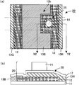
- FIG. 2 is a schematic diagram illustrating a color filter substrate according to Embodiment 1, where (a) is a plan view and (b) is a cross-sectional view taken along line X1-Y1 in (a).
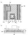
- FIG. 5 is a schematic diagram illustrating a color filter substrate of Embodiment 2, where (a) is a plan view and (b) is a cross-sectional view taken along line X2-Y2 in (a).
- FIG. 10 is a schematic diagram illustrating a conventional color filter substrate, where (a) is a plan view and (b) is a cross-sectional view taken along line X3-Y3 in (a).
- FIG. 6 is a schematic plan view showing another color filter substrate of Embodiment 2.
- FIG. 6 is a schematic plan view showing a color filter substrate of Embodiment 3.
- FIG. 10 is a schematic plan view illustrating a comparative example of a color filter substrate of Embodiment 3.
- FIG. 10 is a schematic diagram illustrating a comparative example of a color filter substrate of Embodiment 3, where (a) is a plan view and (b) is a cross-sectional view taken along line X4-Y4 in (a).
- the liquid crystal display device of Embodiment 1 is a TN mode liquid crystal display device including a TFT substrate and a color filter substrate facing each other, and the distance between both substrates is kept constant by a laminated spacer.
- the TFT substrate and the color filter substrate are bonded together with a sealant, and a liquid crystal material containing liquid crystal molecules having positive dielectric anisotropy is filled between the two substrates to form a liquid crystal layer.
- the liquid crystal layer exhibits a horizontal alignment mode in which liquid crystal molecules are aligned in parallel with both substrates in a state where no voltage is applied between the two substrates.
- a TFT substrate has a general configuration. For example, wiring such as a source line, a gate line, and a Cs line (retention capacitor wiring), a TFT serving as a switching element, an insulating layer, a pixel, It has an electrode and an alignment film.
- FIG. 1A and 1B are schematic views showing a color filter substrate according to Embodiment 1 of the present invention.
- FIG. 1A is a plan view
- FIG. 1B is a cross-sectional view taken along line X1-Y1 in FIG.
- the color filter substrate of Embodiment 1 includes a black matrix 12, a pixel colored layer (red) 13R, and a pixel element on one main surface side (liquid crystal layer side) of a transparent substrate 11.
- a colored layer (green) 13G, a pixel colored layer (blue) 13B, a laminated spacer 15, a counter electrode 17, and an alignment film are provided.
- the black matrix 12 is a light shielding layer having a picture element opening.
- the picture element colored layer (red) 13R, the picture element picture colored layer (green) 13G, and the picture element colored layer (blue) 13B are arranged side by side in correspondence with one color for each picture element.
- the black matrix 12 is made of a material containing a resin, and is formed along the source line of the TFT substrate that is the counter substrate and extends in the vertical direction in FIG. 1A (source light shielding portion). It has the part (gate light-shielding part and Cs light-shielding part) extended in the left-right direction of Fig.1 (a) formed along the gate line and Cs line.
- FIG. 1A only the periphery of the laminated spacer 15 is shown.
- the gate light shielding part and the Cs light shielding part are arranged in parallel to each other, and the source light shielding part, the gate light shielding part and the Cs light shielding part are arranged orthogonal to each other.
- an opening region surrounded by the source light-shielding portion and the gate light-shielding portion is approximately one picture element (a single color region constituting a pixel, a sub-pixel).
- each picture element is surrounded by the source light shielding portion and the gate light shielding portion of the black matrix 12.
- the black matrix 12 has a width that is greater than that of the other portion when the substrate 11 is viewed in plan, at a portion disposed between the pixel colored layer (green) 13G and the pixel colored layer (blue) 13B. It also has a wide part that is thicker.
- the black matrix 12 has a protruding portion 12a protruding in a convex shape on the pixel colored layer (blue) 13B side.
- the laminated spacer 15 is mainly provided on the protruding portion 12a.
- the pixel colored layer in contact with the protruding portion 12a overlaps the protruding portion 12a along the outline of the protruding portion 12a.
- the black matrix 12 has a wide portion, and the laminated spacer 15 is provided on the protruding portion 12a, whereby light leakage due to liquid crystal alignment disorder in the vicinity of the laminated spacer 15 can be suppressed.
- the aperture ratio may decrease.
- the pattern of the black matrix 12 is a gate as much as possible. It is preferable to arrange so as to overlap the pattern of the light shielding member provided on the TFT substrate such as a line or a Cs line. Thereby, it is possible to further suppress the light leakage caused by the alignment disorder of the liquid crystal in the vicinity of the laminated spacer 15.
- the width of the wide portion is not particularly limited, but is preferably larger than the diameter of the column portion 14 of the laminated spacer 15 described later. Since the diameter of the pillar portion 14 in plan view is usually about 10 to 30 ⁇ m, the vertical width of the wide portion (vertical direction in FIG. 1 (a)) and the horizontal width (of FIG. 1 (a)). The horizontal direction is preferably about 30 to 70 ⁇ m and 36 to 100 ⁇ m, respectively. On the other hand, the lateral width of the thin portion other than the wide portion of the black matrix 12 may normally be about 6 to 30 ⁇ m.
- the pixel colored layer (red) 13R, the pixel colored layer (green) 13G, and the pixel colored layer (blue) 13B are formed with pixel pixel openings (black matrix 12) adjacent to each other in the horizontal direction of FIG. (Not in the area).
- the picture element openings in which the picture element colored layer (red) 13R, the picture element colored layer (green) 13G, and the picture element colored layer (blue) 13B are arranged are a red picture element, a blue picture element, and a green picture element, respectively.
- a black matrix 12 is arranged between the red picture element, the blue picture element, and the green picture element, and the picture element colored layer (red) 13R, the picture element colored layer.
- the (green) 13G and the pixel colored layer (blue) 13B are arranged so that the end portions thereof overlap the end portions of the black matrix 12, respectively.
- the color filter substrate 10 according to the first embodiment is a stripe-arranged color filter substrate in which red, blue, and green picture elements are arranged in a stripe pattern.
- one pixel (the minimum unit constituting a display image) is configured by the red picture element, the blue picture element, and the green picture element that are adjacent in the left-right direction in FIG.
- the TFT substrate is provided with a TFT as a switching element and a pixel electrode connected to the TFT corresponding to each picture element.
- the laminated spacer 15 includes a wide portion (mainly a protruding portion 12 a) of the black matrix 12, a pedestal portion on which the spacer coloring layer 16 and the counter electrode 17 are laminated, and a column portion 14 that adjusts the height of the laminated spacer 15. .
- the spacer colored layer 16 has the same color as the pixel colored layer (in the first embodiment, the pixel colored layer (blue) 13B) in contact with the protruding portion 12a.
- a separation portion 18 that is a portion where no colored layer is disposed is formed on the protruding portion 12a.
- the spacer colored layer 16 and the pixel colored layer (blue) 13 ⁇ / b> B are separated by the separation portion 18.
- the spacer colored layer 16 and the pixel colored layer (blue) 13B are connected only to the base of the protruding portion 12a (around the center of the wide portion).
- the spacer coloring layer 16 and the pixel coloring layer (blue) 13B have a continuous shape continuously connected, and the pixel coloring layer ( Blue) 13B can also be said to function as the spacer coloring layer 16.
- the separated portion 18 is provided in the pixel colored layer (blue) 13B of the portion located on the protruding portion 12a, the region where the pixel colored layer (blue) 13B and the protruding portion 12a overlap is provided. The vertical and horizontal widths can be reduced.
- the region where the pixel colored layer (blue) 13B and the protruding portion 12a overlap can be set to be thin in a linear shape.
- step difference by the side of the pixel opening part of the pixel colored layer (blue) 13B resulting from the protrusion part 12a can be reduced.
- the pixel colored layer (green) 13G does not need to be used as a pedestal portion of the laminated spacer 15, it can be superimposed on the black matrix 12 along the outline of the black matrix 12. Therefore, it is possible to suppress the occurrence of alignment disorder of the liquid crystal in the vicinity of the laminated spacer 15.
- the spacer colored layer 16 and the pixel colored layer (blue) 13B have a continuous shape, the spacer colored layer 16 and the pixel colored layer (blue) 13B are formed in the same process. Can be formed. As a result, the spacer coloring layer 16 and the pixel coloring layer (blue) 13B overlap to increase the step on the pixel opening side of the laminated spacer 15, or the height of the pedestal of the laminated spacer 15 becomes unstable. And the stable formation of the pedestal portion of the laminated spacer 15 can be easily performed.
- the pedestal portion of the laminated spacer 15, the protrusion 12 a, the spacer coloring layer 16, and the counter electrode 17 are laminated, so that the thickness of the column portion 14 can be reduced by using the height of the pedestal portion. it can.
- the laminated spacer 15 can be formed at a stable height.
- the protruding portion 12a and the spacer colored layer 16 are laminated, even if a defective portion such as a pinhole is generated in the protruding portion 12a, the defective portion is conspicuous by covering the defective portion with the spacer colored layer 16. Can be eliminated.
- the pixel colored layer overlapping the protruding portion 12a has a lower transmittance than the pixel colored layer (green) 13G.
- the colored layer (red) 13R or the pixel colored layer (blue) 13B is preferable.
- the pixel colored layer (red) 13R caused by the black matrix 12 is compared with the case where the black matrix 12 is formed using a metal film.
- the pixel colored layer (green) 13G and the pixel colored layer (blue) 13B are likely to have large steps, and in particular, the pixel colored layer resulting from the protruding portion 12a (in the first embodiment, the pixel colored layer (blue) 13B) tends to be particularly large.
- the color filter substrate 10 of Embodiment 1 as described above, it is possible to effectively reduce the level difference of the pixel colored layer caused by the protruding portion 12a. Thereby, it is possible to suppress the occurrence of alignment disorder of the liquid crystal in the vicinity of the laminated spacer 15.
- the level difference of the elementary colored layer in the first embodiment, the picture element colored layer (blue) 13B) tends to be particularly large.
- the color filter substrate 10 of Embodiment 1 it is possible to effectively reduce the level difference of the pixel colored layer caused by the protruding portion 12a. Thereby, it is possible to suppress the occurrence of disorder in the alignment of the liquid crystal in the vicinity of the laminated spacer 15 without increasing the number of steps.
- the black matrix 12 has a wide portion including the protruding portion 12a. Therefore, in the configuration like the conventional color filter substrate 110 shown in FIG.
- the level difference of the colored layer in the first embodiment, the pixel colored layer (blue) 13B) tends to be large.
- the color filter substrate 10 of Embodiment 1 it is possible to effectively reduce the level difference of the pixel colored layer caused by the protruding portion 12a. Thereby, it is possible to suppress the occurrence of alignment disorder of the liquid crystal in the vicinity of the laminated spacer 15.
- the manufacturing method of the liquid crystal display device of Embodiment 1 is demonstrated. Since the steps other than the manufacturing process of the color filter substrate 10 such as the TFT substrate manufacturing process and the panel assembling process are the same as the conventional processes, the manufacturing method of the color filter substrate will be mainly described here.
- the color filter substrate 10 is formed using a photolithography (photolithography) method, a printing method, or the like. This time, the case where it is formed by the photolithography method will be described with an example. More specifically, first, a general negative or positive black photosensitive resin composition (for example, a negative or positive photosensitive acrylic resin composition containing carbon black or a pigment) is formed on the substrate 11. After forming the black photosensitive resin film using, the black photosensitive resin film is patterned by a photolithography method, thereby forming the black matrix 12 in a shape having the protruding portions 12a (wide portions). The film thickness of the black matrix 12 is preferably 0.5 to 4 ⁇ m.
- the shape of the protrusion 12a is not particularly limited, and may be a trapezoidal shape, a circular shape, an elliptical shape, or the like in addition to the rectangular shape shown in FIG. Further, as a method for forming the black matrix 12, a printing method or the like may be used.
- the layout of the black matrix 12 is not particularly limited as long as it is formed so as to shield at least a part between adjacent picture elements, and may have only a source light shielding part and a gate light shielding part. As shown in FIG. Moreover, you may further have a part for light-shielding the switching element of a TFT substrate.
- a glass substrate is often used, but for example, a plastic film or a plastic sheet may be used. If necessary, in order to improve the adhesion of the black matrix 12, the pixel colored layer (red) 13R, the pixel colored layer (green) 13G, and the pixel colored layer (blue) 13B to the substrate 11, the substrate 11 A thin film that improves the adhesiveness may be formed beforehand.
- a negative or positive liquid color resist for example, a negative or positive photosensitive acrylic resin composition containing a pigment
- a negative or positive film color resist for example, By applying or transferring a negative or positive photosensitive acrylic film containing a pigment or the like, a red photosensitive resin film (color film) is formed.
- a pixel colored layer (red) 13R is formed in a region including a pixel opening (region where the black matrix 12 is not formed).
- the film thickness of the pixel colored layer (red) 13R in the pixel opening is preferably 0.5 to 3 ⁇ m.
- the end of the pixel colored layer (red) 13R on the black matrix 12 side overlaps with the black matrix 12, and the pixel colored layer (red) 13R has a step due to the black matrix 12.
- the film thickness of the region overlapping the black matrix 12 of the pixel colored layer (red) 13R is smaller than the film thickness at the pixel opening.
- the width of the region where the pixel colored layer (red) 13R and the black matrix 12 overlap is preferably 15 ⁇ m or less, and more preferably 6 ⁇ m or less. Thereby, the film thickness reduction effect of the area
- the step difference in the region overlapping the black matrix 12 of the pixel colored layer (red) 13R is about 0.2 to 4 ⁇ m.
- the pixel colored layer (red) 13R may be formed by a printing method or the like using a resin having no photosensitivity.
- a negative or positive liquid color resist for example, a negative or positive photosensitive acrylic resin composition containing a pigment
- a negative or positive film color resist for example, A blue photosensitive resin film (color film) is formed by applying or transferring a negative or positive photosensitive acrylic film containing a pigment.
- the pixel colored layer (blue) 13B is formed in a region including the pixel opening (region where the black matrix 12 is not formed).
- the film thickness of the pixel colored layer (blue) 13B in the pixel opening is preferably 0.5 to 3 ⁇ m.
- the film thickness of the spacer colored layer 16 is generally the same as the film thickness in the pixel opening of the pixel colored layer (blue) 13B.
- the end of the pixel colored layer (blue) 13B on the black matrix 12 side overlaps with the black matrix 12, and the pixel colored layer (blue) 13B has a step due to the black matrix 12.
- the film thickness of the region overlapping the black matrix 12 of the pixel colored layer (blue) 13B is smaller than the film thickness at the pixel opening.
- a separation portion 18 is formed in an area overlapping with the protruding portion 12a so that the pixel colored layer (blue) 13B and the spacer colored layer 16 are connected only at the base of the protruding portion 12a.
- the width of the separating portion 18 may be about 2 to 10 ⁇ m.
- the width of the region where the pixel colored layer (blue) 13B and the black matrix 12 overlap is preferably 15 ⁇ m or less, and more preferably 6 ⁇ m or less, so that the region overlapping the black matrix 12 of the pixel colored layer (blue) 13B The film thickness reducing effect can be sufficiently exhibited.
- the level difference of the region overlapping the black matrix 12 of the pixel colored layer (blue) 13B is about 0.2 to 4 ⁇ m.
- the pixel colored layer (blue) 13B may be formed by a printing method or the like using a resin having no photosensitivity.
- a negative or positive liquid color resist for example, a negative or positive photosensitive acrylic resin composition containing a pigment
- a negative or positive film color resist for example, A green photosensitive resin film (color film) is formed by applying or transferring a negative or positive photosensitive acrylic film containing a pigment.
- a pixel colored layer (green) 13G is formed in a region including the pixel element opening.
- the film thickness of the pixel colored layer (green) 13G in the pixel opening is preferably 0.5 to 3 ⁇ m.
- the end of the pixel colored layer (green) 13G on the black matrix 12 side overlaps with the black matrix 12, and the pixel colored layer (green) 13G has a step due to the black matrix 12.
- the film thickness of the region overlapping the black matrix 12 of the pixel colored layer (green) 13G is smaller than the film thickness at the pixel opening.
- the width of the region where the pixel colored layer (green) 13G and the black matrix 12 overlap is preferably 15 ⁇ m or less, and more preferably 6 ⁇ m or less, so that the region of the region overlapping the black matrix 12 of the pixel colored layer (green) 13G The film thickness reducing effect can be sufficiently exhibited.
- the step difference in the region overlapping the black matrix 12 of the pixel colored layer (green) 13G is about 0.2 to 4 ⁇ m.
- the pixel colored layer (green) 13G may be formed by a printing method or the like using a resin having no photosensitivity.
- the order of forming the pixel colored layer (red) 13R, the pixel colored layer (green) 13G, and the pixel colored layer (blue) 13B is not limited to this, and can be set as appropriate.
- the color of the spacer coloring layer 16 is not particularly limited. However, from the viewpoint of suppressing light leakage from the laminated spacer 15, in the case of using red, green, and blue pixel coloring layers, the pixel coloring is performed. It is preferable that the pixel colored layer (red) 13R or the pixel colored layer (blue) 13B has a lower transmittance than the layer (green) 13G. From the same viewpoint, it is preferable that the laminated spacer 15 is selectively provided on a red picture element or a blue picture element.
- the counter electrode 17 is formed so as to cover the black matrix 12, the pixel colored layer (red) 13R, the pixel colored layer (green) 13G, the pixel colored layer (blue) 13B, and the spacer colored layer 16.
- a transparent electrode film can be used as the counter electrode 17, and examples of the material include indium / tin oxide (ITO) and InTiO 3 .
- ITO indium / tin oxide
- InTiO 3 InTiO 3
- a sputtering method is mentioned, for example.
- the photosensitive resin film is formed by photolithography. Is patterned.
- the column part 14 can be formed on the spacer colored layer 16.
- the material of the column portion 14 is not particularly limited, but can be easily formed by using a photolithography method by using a photosensitive resin.
- the photosensitive resin may be a photosensitive resin containing a black pigment, a photosensitive resin containing a pigment (color resist), or a transparent photosensitive resin containing no pigment. May be. Note that the height of the column portion 14 may be appropriately set according to a desired cell gap. Further, the column portion 14 may be formed on the TFT substrate side. Further, the column portion 14 may be formed by a printing method or the like using a resin having no photosensitivity.
- an alignment film is formed, and the alignment film is rubbed to complete the color filter substrate 10.
- An example of the material of the alignment film is a thermosetting polyimide resin.
- the liquid crystal display device of Embodiment 1 can be completed by performing a cell assembly process and a module assembly process using the color filter substrate 10 manufactured as described above and a general TFT substrate. it can.
- the liquid crystal display device of the first embodiment it is possible to suppress the occurrence of alignment disorder of the liquid crystal in the vicinity of the multilayer spacer without increasing the number of steps. As a result, it is possible to suppress the occurrence of light leakage due to liquid crystal alignment disorder and to realize a TN mode liquid crystal display device with a high contrast ratio.
- the liquid crystal display device of the second embodiment is a TN mode liquid crystal display device including a TFT substrate and a color filter substrate facing each other.
- 2A and 2B are schematic views showing the color filter substrate of Embodiment 2, wherein FIG. 2A is a plan view and FIG. 2B is a cross-sectional view taken along line X2-Y2 in FIG.
- FIG. 2 the same members as those in the first embodiment are denoted by the same reference numerals, and the description thereof is omitted.
- the color filter substrate 20 of Embodiment 2 includes a black matrix 12 that is a light shielding layer having a picture element opening on one main surface side (liquid crystal layer side) of a transparent substrate 11, and each A pixel colored layer (red) 13R, a pixel colored layer (green) 13G, and a pixel colored layer (blue) 13B, a laminated spacer 25, a counter electrode 17, an alignment film, Is provided.
- a region sandwiched between broken lines in FIG. 2 indicates a region shielded by a light shielding member provided on the TFT substrate.
- the black matrix 12 When the substrate 11 is viewed in plan, the black matrix 12 is wider in the portion disposed between the pixel colored layer (blue) 13B and the pixel colored layer (red) 13R than the other portions. It has a wide part. More specifically, the black matrix 12 has a protruding portion 12b protruding in a convex shape on the pixel colored layer (blue) 13B side, and a contour line on the wide pixel colored layer (red) 13R side. Is shorter than the contour line on the pixel colored layer (blue) 13B side of the wide part.
- the pixel colored layer in contact with the protruding portion 12b (in the second embodiment, the pixel colored layer (blue) 13B) has a recessed planar shape corresponding to the protruding portion 12b.
- the laminated spacer 25 is mainly provided on the protruding portion 12b. More specifically, the laminated spacer 25 adjusts the height of the wide portion (mainly the protruding portion 12b) of the black matrix 12, the pedestal portion on which the spacer coloring layer 26 and the counter electrode 17 are laminated, and the height of the laminated spacer 25. Column part 14.
- the spacer coloring layer 26 is connected to the pixel coloring layer (red) 13R adjacent to the pixel coloring layer (in the second embodiment, the pixel coloring layer (blue) 13B in the second embodiment) with the laminated spacer 25 interposed therebetween.
- the spacer colored layer 26 and the pixel colored layer (red) 13R have a continuous and integral shape, and the protruding portion of the pixel colored layer (red) 13R functions as the spacer colored layer 26. It can be said that it is.
- the region where the spacer coloring layer 26 and the black matrix 12 overlap has, for example, a vertical width (vertical direction of FIG. 2A) of 20 to 60 ⁇ m and a horizontal width (horizontal direction of FIG.
- the protrusion 12b has, for example, a vertical width (vertical direction in FIG. 2A) of 30 to 70 ⁇ m and a horizontal width (horizontal direction of FIG. 2A) of 36 to 76 ⁇ m.
- the vertical width of the region where the spacer coloring layer 26 and the black matrix 12 overlap can be reduced.
- the generated region is reduced, and the light can be easily shielded by using a light shielding member provided on the TFT substrate such as a gate line and a Cs line without adding a new member.
- the vertical and horizontal widths of the pixel colored layer (blue) 13B in the region overlapping the protruding portion 12b are increased. Can be reduced. That is, the region where the pixel colored layer (blue) 13B and the protruding portion 12b overlap can be set to be thin in a linear shape. As a result, the step on the pixel opening side of the pixel colored layer (blue) 13B due to the protruding portion 12b can be reduced, and the occurrence of liquid crystal alignment disorder in the vicinity of the laminated spacer 25 can be suppressed.
- the spacer colored layer 26 is connected to the pixel colored layer (red) 13R, so that the effect of reducing the thickness of the spacer colored layer 26 is much exhibited. Otherwise, the step on the pixel opening side of the pixel colored layer (red) 13R becomes large, and the alignment disorder of the liquid crystal tends to occur.
- the region where the alignment disorder of the liquid crystal is likely to occur is a region where the spacer colored layer 26 and the black matrix 12 overlap, and the pixel colored layer (blue) disposed on the protruding side of the protruding portion 12b.
- the color filter substrate 20 can also suppress the occurrence of liquid crystal alignment disorder in the vicinity of the laminated spacer 25 as compared with the conventional case.
- a light shielding member provided on the TFT substrate for example, a wiring such as a gate line or a Cs line is used. It is possible to easily shield light from a region where liquid crystal alignment is liable to occur without adding a member.
- the spacer colored layer 26 and the pixel colored layer (red) 13R are connected, the spacer colored layer 26 and the pixel colored layer (red) 13R can be formed in the same process. As a result, the spacer colored layer 26 and the pixel colored layer (red) 13R overlap to increase the step on the pixel opening side of the laminated spacer 25, or the height of the pedestal of the laminated spacer 25 becomes unstable. And the stable formation of the pedestal portion of the laminated spacer 25 can be easily performed.
- the color of the spacer coloring layer 26 is not particularly limited, but from the viewpoint of suppressing light leakage from the laminated spacer 25, when using three colored pixel colored layers of red, green and blue, It is preferable that the pixel colored layer (red) 13R or the pixel colored layer (blue) 13B have a lower transmittance than the element colored layer (green) 13G. From the same viewpoint, the pixel colored layer adjacent to the spacer colored layer 26 and the laminated spacer 25 side also has a pixel colored layer (red) 13R or a pixel colored lower in transmittance than the pixel colored layer (green) 13G. The layer (blue) 13B is preferable.
- the liquid crystal display device of the third embodiment is a TN mode liquid crystal display device including a TFT substrate and a color filter substrate facing each other.
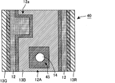
- FIG. 6 is a schematic plan view showing the color filter substrate of the third embodiment.
- FIG. 7 is a schematic plan view showing a comparative example of the color filter substrate of the third embodiment,
- FIG. 8 is a schematic diagram showing a comparative example of the color filter substrate of the third embodiment, and
- the color filter substrate 30 of Embodiment 3 includes a black matrix 12, a pixel colored layer (red) 13 ⁇ / b> R, and a picture element picture on one main surface side (liquid crystal layer side) of the transparent substrate 11.
- Element colored layer (green) 13G, picture element colored layer (blue) 13B, laminated spacer 35, counter electrode and alignment film are provided.
- the black matrix 12 is a light shielding layer having a picture element opening.
- the picture element colored layer (red) 13R, the picture element picture colored layer (green) 13G, and the picture element colored layer (blue) 13B are arranged side by side in correspondence with one color for each picture element.
- the laminated spacer 35 is disposed on the island portion 12 ⁇ / b> A that is an independent island-shaped light shielding layer that is not connected to the black matrix 12.
- a picture element colored layer (blue) 13B is arranged around the island part 12A, and ends of the island part 12A and the picture element colored layer (blue) 13B overlap.
- As a pedestal portion of the laminated spacer 35 an island portion 12A and a spacer coloring layer 36 provided so as to overlap the island portion 12A are used.
- the width of the island portion 12A is not particularly limited, but is preferably larger than the diameter of the column portion 14. More specifically, since the diameter of the pillar portion 14 in plan view is usually about 10 to 30 ⁇ m, the vertical width (vertical direction in FIG.
- the width (left and right direction in FIG. 6) of the island portion 12A is 20 to 80 ⁇ m, The width (left and right direction in FIG. 6) is preferably 20 to 80 ⁇ m.
- the spacer colored layer 36 is an island-shaped colored layer provided separately from the pixel colored layer (in the third embodiment, the pixel colored layer (blue) 13B) arranged around the island 12A. And the same color as the pixel colored layer (blue) 13B. That is, it can be said that the separating portion 38 is provided on the island portion 12A along the outline of the island portion 12A.
- the width of the separating portion 38 may be about 2 to 10 ⁇ m.
- the film thickness of the region overlapping the island portion 12A of the colored layer (blue) 13B is smaller than the film thickness at the pixel opening.
- the width of the region where the pixel colored layer (blue) 13B and the island portion 12A overlap is preferably 15 ⁇ m or less, more preferably 6 ⁇ m or less, thereby overlapping the island portion 12A of the pixel colored layer (blue) 13B.
- the film thickness reduction effect in the region can be sufficiently exhibited. More specifically, the level difference in the region overlapping the island portion 12A of the pixel colored layer (blue) 13B is about 0.2 to 4 ⁇ m.
- the spacer coloring layer 36 is arranged on the island portion 12A independently in an island shape, so that the vertical and horizontal directions of the pixel coloring layer (blue) 13B in the region overlapping the island portion 12A are obtained.
- the width can be reduced.
- the level difference of the pixel colored layer (blue) 13B caused by the island portion 12A can be reduced, so that occurrence of alignment disorder of the liquid crystal in the vicinity of the laminated spacer 35 can be suppressed.
- the spacer colored layer (blue) 13B and the spacer colored layer 36 provided in the picture element in which the laminated spacer 35 is arranged are the same color, the spacer colored layer 36 and the pixel colored layer (blue) 13B Can be formed in the same step. As a result, the spacer colored layer 36 and the pixel colored layer (blue) 13B may overlap with each other, resulting in a large step around the laminated spacer 35 and an unstable height of the pedestal of the laminated spacer 35. Is eliminated, and the pedestal portion of the laminated spacer 35 can be easily formed stably.
- the black matrix 12 disposed between the pixel colored layer (red) 13R, the pixel colored layer (green) 13G, and the pixel colored layer (blue) 13B and having a wide portion 12a; Although the form which provides the island part 12A arrange
- the entire island portion 12A is covered with the pixel colored layer (blue) 13B, and the island portion 12A and the pixel colored layer (blue) in the region overlapping the island portion 12A. 13B is used as a pedestal for the laminated spacer 45. That is, in the color filter substrate 40, the portion of the pixel colored layer (blue) 13B that overlaps the island portion 12A functions as a spacer colored layer.
- the separation portion is not provided on the island portion 12A, and the entire island portion 12A is covered with the pixel colored layer (blue) 13B.
- the vertical and horizontal widths of the pixel colored layer (blue) 13B are large. As a result, the level difference of the pixel colored layer (blue) 13B due to the island portion 12A cannot be sufficiently reduced, and liquid crystal alignment disorder occurs in the vicinity of the laminated spacer 35.
- the island portion 12 ⁇ / b> A and the spacer colored layer 56 disposed so as to overlap the island portion 12 ⁇ / b> A are used as the pedestal portion of the laminated spacer 55.
- the spacer colored layer 56 has a color different from that of the pixel colored layer (blue) 13B disposed around the island portion 12A.
- the spacer colored layer 56 and the pixel colored layer (blue) 13B have different colors, and the spacer colored layer 56 and the pixel colored layer (blue) 13B are formed in different steps. Therefore, in the process of forming the spacer colored layer 56 and the pixel colored layer (blue) 13B, when a misalignment or a finished width shift occurs, the spacer colored layer 56 and the pixel colored layer (blue) 13B are formed. And the height of the step in the vicinity of the laminated spacer 55 may increase, or the height of the pedestal of the laminated spacer 55 may become unstable. In order to eliminate such a concern, since it is necessary to perform the process of forming the spacer colored layer 56 and the pixel colored layer (blue) 13B with high accuracy, it can be realized more easily. It can be said that the embodiment 3 is superior.
- the light shielding layer is formed before the pixel colored layer and the spacer colored layer, that is, the end of the pixel colored layer is disposed above the black matrix, and the pixel coloring is performed.
- the mode in which the layer has a step due to the black matrix has been described, in the region where the colored layer (the pixel colored layer, the first, second and third spacer colored layers) and the light shielding layer overlap, the respective layers overlap.
- the order is not limited, and any layer may be on the upper layer side.
- the pixel colored layer and the spacer colored layer are formed before the black matrix, the black matrix is disposed on the pixel colored layer and the spacer colored layer, and the black matrix is derived from the pixel colored layer and the spacer colored layer. Even in the form having a step, the height of the step of the black matrix due to the pixel colored layer and the spacer colored layer can be reduced, and the occurrence of alignment disorder of the liquid crystal in the vicinity of the laminated spacer can be suppressed.
- FIG. 5 is a schematic plan view showing another color filter substrate of the second embodiment.
- the members already described are denoted by the same reference numerals and description thereof is omitted.
- a region sandwiched between broken lines in FIG. 5 indicates a region shielded by a light shielding member provided on the TFT substrate.
- the black matrix 12 may have a protruding portion 12c that protrudes on the opposite side of the protruding portion 12b.
- the pixel colored layer (in the second embodiment, the pixel colored layer (red) 13R in the second embodiment) that touches the smaller protruding portion 12c (the shorter outline of the wide portion) may be used as the pedestal of the laminated spacer 25.
- the laminated spacers 15, 25, and 35 instead of forming the column part 14, have a pixel colored layer (red) 13 R, a pixel colored layer (green) 13 G, and a pixel colored layer (blue) )
- a pixel colored layer (red) 13 R a pixel colored layer (green) 13 G
- a pixel colored layer (blue) 13B a pixel colored layer independent of the pixel colored layer (red) 13R, the pixel colored layer (green) 13G, and the pixel colored layer (blue) 13B
Landscapes
- Physics & Mathematics (AREA)
- Nonlinear Science (AREA)
- General Physics & Mathematics (AREA)
- Optics & Photonics (AREA)
- Mathematical Physics (AREA)
- Chemical & Material Sciences (AREA)
- Crystallography & Structural Chemistry (AREA)
- Liquid Crystal (AREA)
- Optical Filters (AREA)
Abstract
Description
第一の本発明のカラーフィルタ基板における好ましい形態について以下に詳しく説明する。
第一の本発明の好ましい形態として説明した形態については、第二及び第三のカラーフィルタ基板の好ましい形態としても用いることができる。また、第二及び第三のカラーフィルタ基板を備える液晶表示装置は、積層スペーサ近傍における液晶の配向乱れの発生を抑制することができるため、液晶の配向乱れに起因する光漏れを抑制し、コントラスト比の高い液晶表示装置を実現することができる。更に、第二及び第三のカラーフィルタ基板を備える液晶表示装置は、積層スペーサ近傍における液晶の配向乱れに起因する光漏れが発生しやすいTNモードの液晶表示装置に対して本発明は特に有効である。すなわち、上記液晶表示装置は、TNモードであることが好ましい。
実施形態1の液晶表示装置は、互いに対向するTFT基板及びカラーフィルタ基板を備えるTNモードの液晶表示装置であり、積層スペーサによって両基板の間隔が一定に保持されている。また、TFT基板及びカラーフィルタ基板は、シール剤によって貼り合わせられるとともに、両基板の間には正の誘電率異方性を有する液晶分子を含む液晶材料が充填され、液晶層が形成されている。液晶層は、両基板間に電圧が印加されない状態で、液晶分子が両基板に平行に配向された水平配向モードを示す。なお、TFT基板は、一般的な構成を有し、例えば、基板上に、ソースライン、ゲートライン、Csライン(保持容量配線)等の配線と、スイッチング素子であるTFTと、絶縁層と、画素電極と、配向膜とを有する。
実施形態2の液晶表示装置は、実施形態1の液晶表示装置と同様に、互いに対向するTFT基板及びカラーフィルタ基板を備えるTNモードの液晶表示装置である。図2は、実施形態2のカラーフィルタ基板を示す模式図であり、(a)は平面図であり、(b)は(a)中のX2-Y2線における断面図である。図2において、実施形態1と同一の部材には同一の符号を付記し、説明は省略する。
実施形態3の液晶表示装置は、実施形態1及び2の液晶表示装置と同様に、互いに対向するTFT基板及びカラーフィルタ基板を備えるTNモードの液晶表示装置である。図6は、実施形態3のカラーフィルタ基板を示す平面模式図である。また、図7は、実施形態3のカラーフィルタ基板の比較例を示す平面模式図であり、図8は、実施形態3のカラーフィルタ基板の比較例を示す模式図であり、(a)は平面図であり、(b)は(a)中のX4-Y4線における断面図である。図6~8において、実施形態1と同一の部材については同一の符号を付記し、説明を省略する。
11、111:基板
12、112:ブラックマトリクス
12a、12b、12c、112a:突出部
12A:島部
13R、113R:絵素着色層(赤)
13G、113G:絵素着色層(緑)
13B、113B:絵素着色層(青)
14、114:柱部
15、25、35、45、55、115:積層スペーサ
16、26、36、56:スペーサ着色層
17、117:対向電極
18、38:離間部
213a、213b、213c:着色層の端部
Claims (10)
- 基板上に並置された第一絵素着色層、遮光層及び第二絵素着色層を有するカラーフィルタ基板であって、
該遮光層は、第一幅広部を有し、かつ該第一絵素着色層及び該第二絵素着色層の端部に一部が重なるように配置され、
該第一幅広部は、該第一絵素着色層側に突出した突出部を含み、
該カラーフィルタ基板は、該第一幅広部及び第一スペーサ着色層を含む第一積層スペーサを有し、
該第一スペーサ着色層は、該第一絵素着色層と同色であり、かつ該突出部の付け根のみで該第一絵素着色層と繋がることを特徴とするカラーフィルタ基板。 - 前記カラーフィルタ基板は、前記第一絵素着色層、前記遮光層及び前記第二絵素着色層を覆うオーバーコート層が設けられていないことを特徴とする請求項1記載のカラーフィルタ基板。
- 前記遮光層は、樹脂を含むことを特徴とする請求項1又は2記載のカラーフィルタ基板。
- 前記第一絵素着色層及び前記第二絵素着色層は、端部が前記遮光層上に配置され、かつ前記遮光層に起因する段差を有することを特徴とする請求項1~3のいずれかに記載のカラーフィルタ基板。
- 前記遮光層は、端部が前記第一絵素着色層及び前記二絵素着色層上に配置され、かつ前記第一絵素着色層及び前記第二絵素着色層に起因する段差を有することを特徴とする請求項1~3のいずれかに記載のカラーフィルタ基板。
- 請求項1~5のいずれかに記載のカラーフィルタ基板と、該カラーフィルタ基板に対向する対向基板と、該カラーフィルタ基板及び該対向基板の間に狭持された液晶層とを備えることを特徴とする液晶表示装置。
- 上記液晶表示装置は、ねじれネマチックモードであることを特徴とする請求項6記載の液晶表示装置。
- 基板上に並置された第一絵素着色層、遮光層及び第二絵素着色層を有するカラーフィルタ基板であって、
該遮光層は、少なくとも該第一絵素着色層側に突出した第二幅広部を有し、かつ該第一絵素着色層及び該第二絵素着色層の端部に一部が重なるように配置され、
該カラーフィルタ基板は、該第二幅広部及び第二スペーサ着色層を含む第二積層スペーサを有し、
該第二幅広部の該第二絵素着色層側の輪郭線は、該第二幅広部の該第一絵素着色層側の輪郭線よりも短く、
該第二スペーサ着色層は、該第二絵素着色層と同色であり、かつ該第二絵素着色層と繋がることを特徴とするカラーフィルタ基板。 - 請求項8記載のカラーフィルタ基板と、該カラーフィルタ基板に対向する対向基板と、該カラーフィルタ基板及び該対向基板の間に挟持された液晶層とを備える液晶表示装置であって、
該対向基板は、平面視されたときに、該カラーフィルタ基板の前記第二スペーサ着色層と前記遮光層とが重なる領域に遮光部材を有することを特徴とする液晶表示装置。 - 絵素着色層と、該絵素着色層に囲まれた島状の遮光層とが基板上に並置されたカラーフィルタ基板であって、
該遮光層及び該絵素着色層は、端部が重なりあい、
該カラーフィルタ基板は、該遮光層及び第三スペーサ着色層を含む第三積層スペーサを有し、
該第三スペーサ着色層は、該絵素着色層と同色であり、かつ該絵素着色層から分離して設けられていることを特徴とするカラーフィルタ基板。
Priority Applications (6)
| Application Number | Priority Date | Filing Date | Title |
|---|---|---|---|
| US12/995,496 US20110080543A1 (en) | 2008-07-15 | 2009-04-09 | Color filter substrate and liquid crystal display device |
| EP09797747A EP2299298A1 (en) | 2008-07-15 | 2009-04-09 | Color filter substrate and liquid crystal display device |
| JP2010520795A JP5165760B2 (ja) | 2008-07-15 | 2009-04-09 | カラーフィルタ基板及び液晶表示装置 |
| CN2009801199749A CN102047153A (zh) | 2008-07-15 | 2009-04-09 | 滤色器基板和液晶显示装置 |
| BRPI0915784A BRPI0915784A2 (pt) | 2008-07-15 | 2009-04-09 | substrato de filtro de cor e dispositivo de exibição de cristal líquido |
| RU2011105405/28A RU2469362C2 (ru) | 2008-07-15 | 2009-04-09 | Подложка цветового фильтра и жидкокристаллическое устройство отображения |
Applications Claiming Priority (2)
| Application Number | Priority Date | Filing Date | Title |
|---|---|---|---|
| JP2008-183637 | 2008-07-15 | ||
| JP2008183637 | 2008-07-15 |
Publications (1)
| Publication Number | Publication Date |
|---|---|
| WO2010007819A1 true WO2010007819A1 (ja) | 2010-01-21 |
Family
ID=41550228
Family Applications (1)
| Application Number | Title | Priority Date | Filing Date |
|---|---|---|---|
| PCT/JP2009/057271 Ceased WO2010007819A1 (ja) | 2008-07-15 | 2009-04-09 | カラーフィルタ基板及び液晶表示装置 |
Country Status (7)
| Country | Link |
|---|---|
| US (1) | US20110080543A1 (ja) |
| EP (1) | EP2299298A1 (ja) |
| JP (1) | JP5165760B2 (ja) |
| CN (1) | CN102047153A (ja) |
| BR (1) | BRPI0915784A2 (ja) |
| RU (1) | RU2469362C2 (ja) |
| WO (1) | WO2010007819A1 (ja) |
Cited By (1)
| Publication number | Priority date | Publication date | Assignee | Title |
|---|---|---|---|---|
| JP2011197600A (ja) * | 2010-03-24 | 2011-10-06 | Dainippon Printing Co Ltd | カラーフィルタ、カラーフィルタの製造方法およびそれを備える液晶表示装置 |
Families Citing this family (6)
| Publication number | Priority date | Publication date | Assignee | Title |
|---|---|---|---|---|
| ES2720365T3 (es) | 2007-03-14 | 2019-07-19 | Wavelight Gmbh | Aparato para el acoplamiento de un elemento al ojo |
| KR101965305B1 (ko) | 2012-08-17 | 2019-04-04 | 삼성디스플레이 주식회사 | 액정 표시 장치 및 그 제조 방법 |
| TWI638209B (zh) * | 2015-05-05 | 2018-10-11 | 友達光電股份有限公司 | 顯示面板 |
| CN205427389U (zh) | 2016-03-17 | 2016-08-03 | 京东方科技集团股份有限公司 | 显示基板及显示装置 |
| CN110147012A (zh) * | 2019-05-05 | 2019-08-20 | 深圳市华星光电半导体显示技术有限公司 | 彩色滤光片基板以及液晶显示装置 |
| CN113075811B (zh) | 2020-01-06 | 2023-08-18 | 群创光电股份有限公司 | 电子装置 |
Citations (10)
| Publication number | Priority date | Publication date | Assignee | Title |
|---|---|---|---|---|
| JPH02308105A (ja) | 1989-05-23 | 1990-12-21 | Mitsubishi Electric Corp | カラーフィルタ及びその製造方法 |
| JPH0534680A (ja) | 1991-07-31 | 1993-02-12 | Nec Corp | アクテイブマトリクスカラー液晶デイスプレイ |
| JPH06308478A (ja) | 1993-04-23 | 1994-11-04 | Toppan Printing Co Ltd | 液晶表示用カラーフィルター |
| JPH112718A (ja) * | 1997-06-12 | 1999-01-06 | Dainippon Printing Co Ltd | カラーフィルタおよびカラー液晶表示装置 |
| JPH11352322A (ja) * | 1998-04-07 | 1999-12-24 | Toray Ind Inc | カラ―フィルタ及びそれを用いたカラ―液晶表示装置 |
| JP2003107493A (ja) * | 2001-10-02 | 2003-04-09 | Toppan Printing Co Ltd | フラットパネルディスプレイ用電極板 |
| JP2006293189A (ja) * | 2005-04-14 | 2006-10-26 | Dainippon Printing Co Ltd | カラーフィルタの製造方法および液晶表示装置 |
| JP2007057762A (ja) | 2005-08-24 | 2007-03-08 | Toray Ind Inc | 液晶表示装置用カラーフィルター基板およびその製造方法 |
| JP2007171620A (ja) | 2005-12-22 | 2007-07-05 | Sharp Corp | 表示装置及びそれに用いるカラーフィルタ基板 |
| JP2008183637A (ja) | 2007-01-26 | 2008-08-14 | Sharp Corp | 保持装置およびこれを有する搬送装置 |
Family Cites Families (5)
| Publication number | Priority date | Publication date | Assignee | Title |
|---|---|---|---|---|
| RU2018892C1 (ru) * | 1992-06-05 | 1994-08-30 | Малое научно-производственное предприятие "ЭЛО" | Жидкокристаллическая цветная дисплейная панель с активной матрицей |
| KR100207135B1 (ko) * | 1994-10-18 | 1999-07-15 | 니시무로 타이죠 | 반사형 액정표시소자 및 그 제조방법 |
| TW589504B (en) * | 1997-06-12 | 2004-06-01 | Sharp Kk | Liquid crystal display device |
| TW475087B (en) * | 1997-09-12 | 2002-02-01 | Toshiba Corp | Active matrix liquid crystal display device |
| JP2004012802A (ja) * | 2002-06-06 | 2004-01-15 | Nec Lcd Technologies Ltd | 液晶表示装置 |
-
2009
- 2009-04-09 EP EP09797747A patent/EP2299298A1/en not_active Withdrawn
- 2009-04-09 RU RU2011105405/28A patent/RU2469362C2/ru not_active IP Right Cessation
- 2009-04-09 BR BRPI0915784A patent/BRPI0915784A2/pt not_active IP Right Cessation
- 2009-04-09 JP JP2010520795A patent/JP5165760B2/ja not_active Expired - Fee Related
- 2009-04-09 US US12/995,496 patent/US20110080543A1/en not_active Abandoned
- 2009-04-09 CN CN2009801199749A patent/CN102047153A/zh active Pending
- 2009-04-09 WO PCT/JP2009/057271 patent/WO2010007819A1/ja not_active Ceased
Patent Citations (10)
| Publication number | Priority date | Publication date | Assignee | Title |
|---|---|---|---|---|
| JPH02308105A (ja) | 1989-05-23 | 1990-12-21 | Mitsubishi Electric Corp | カラーフィルタ及びその製造方法 |
| JPH0534680A (ja) | 1991-07-31 | 1993-02-12 | Nec Corp | アクテイブマトリクスカラー液晶デイスプレイ |
| JPH06308478A (ja) | 1993-04-23 | 1994-11-04 | Toppan Printing Co Ltd | 液晶表示用カラーフィルター |
| JPH112718A (ja) * | 1997-06-12 | 1999-01-06 | Dainippon Printing Co Ltd | カラーフィルタおよびカラー液晶表示装置 |
| JPH11352322A (ja) * | 1998-04-07 | 1999-12-24 | Toray Ind Inc | カラ―フィルタ及びそれを用いたカラ―液晶表示装置 |
| JP2003107493A (ja) * | 2001-10-02 | 2003-04-09 | Toppan Printing Co Ltd | フラットパネルディスプレイ用電極板 |
| JP2006293189A (ja) * | 2005-04-14 | 2006-10-26 | Dainippon Printing Co Ltd | カラーフィルタの製造方法および液晶表示装置 |
| JP2007057762A (ja) | 2005-08-24 | 2007-03-08 | Toray Ind Inc | 液晶表示装置用カラーフィルター基板およびその製造方法 |
| JP2007171620A (ja) | 2005-12-22 | 2007-07-05 | Sharp Corp | 表示装置及びそれに用いるカラーフィルタ基板 |
| JP2008183637A (ja) | 2007-01-26 | 2008-08-14 | Sharp Corp | 保持装置およびこれを有する搬送装置 |
Cited By (1)
| Publication number | Priority date | Publication date | Assignee | Title |
|---|---|---|---|---|
| JP2011197600A (ja) * | 2010-03-24 | 2011-10-06 | Dainippon Printing Co Ltd | カラーフィルタ、カラーフィルタの製造方法およびそれを備える液晶表示装置 |
Also Published As
| Publication number | Publication date |
|---|---|
| JP5165760B2 (ja) | 2013-03-21 |
| JPWO2010007819A1 (ja) | 2012-01-05 |
| CN102047153A (zh) | 2011-05-04 |
| BRPI0915784A2 (pt) | 2015-11-10 |
| US20110080543A1 (en) | 2011-04-07 |
| RU2011105405A (ru) | 2012-08-20 |
| EP2299298A1 (en) | 2011-03-23 |
| RU2469362C2 (ru) | 2012-12-10 |
Similar Documents
| Publication | Publication Date | Title |
|---|---|---|
| KR102122402B1 (ko) | 씨오티 구조 액정표시장치 및 이의 제조방법 | |
| US8698995B2 (en) | Liquid crystal display panel having particular laminate spacer | |
| JP4044090B2 (ja) | カラーフィルタ基板及びそれを備えた液晶表示装置、並びにカラーフィルタ基板の製造方法 | |
| JP5437971B2 (ja) | 液晶表示装置 | |
| JP5151903B2 (ja) | カラーフィルタ基板及びその製造方法並びに液晶表示装置 | |
| JP5379124B2 (ja) | 液晶表示装置 | |
| US20100165266A1 (en) | Production method of color filter substrate, production method of liquid crystal display device, color filter substrate, and liquid crystal display device | |
| JP5165760B2 (ja) | カラーフィルタ基板及び液晶表示装置 | |
| TWI581038B (zh) | 液晶顯示面板 | |
| JP5389258B2 (ja) | 液晶表示装置 | |
| KR20160130045A (ko) | 표시 패널 | |
| CN106896587A (zh) | 液晶显示设备及其制造方法 | |
| CN109976024A (zh) | 彩色滤光片基板及其制造方法、以及显示面板 | |
| JP5894872B2 (ja) | 液晶表示装置 | |
| US20170329177A1 (en) | Liquid Crystal Display Panel, Liquid Crystal Display Apparatus, and Method of Manufacturing Liquid Crystal Display Panel | |
| JP4270296B2 (ja) | 液晶装置、カラーフィルタ基板及び電子機器 | |
| CN109313370B (zh) | 显示面板 | |
| KR102227696B1 (ko) | 씨오티 구조 액정표시장치 | |
| KR20160055320A (ko) | 컬러필터 어레이 기판 및 그 제조방법과 이를 이용한 액정표시장치 | |
| KR20200022556A (ko) | 액정 표시 장치 및 그 제조 방법 | |
| JP2025001952A (ja) | 液晶パネル及び液晶表示装置 | |
| KR102238171B1 (ko) | 컬러필터 어레이기판 제조방법 및 이를 적용한 액정표시소자 제조방법 | |
| JP2024100064A (ja) | 表示パネル用基板、及び表示装置 | |
| JP2024137405A (ja) | 液晶表示パネル | |
| JP2007079354A (ja) | 液晶装置、液晶装置の製造方法、及び、電子機器 |
Legal Events
| Date | Code | Title | Description |
|---|---|---|---|
| WWE | Wipo information: entry into national phase |
Ref document number: 200980119974.9 Country of ref document: CN |
|
| 121 | Ep: the epo has been informed by wipo that ep was designated in this application |
Ref document number: 09797747 Country of ref document: EP Kind code of ref document: A1 |
|
| WWE | Wipo information: entry into national phase |
Ref document number: 4445/KOLNP/2010 Country of ref document: IN |
|
| WWE | Wipo information: entry into national phase |
Ref document number: 2010520795 Country of ref document: JP |
|
| WWE | Wipo information: entry into national phase |
Ref document number: 2009797747 Country of ref document: EP |
|
| NENP | Non-entry into the national phase |
Ref country code: DE |
|
| WWE | Wipo information: entry into national phase |
Ref document number: 2011105405 Country of ref document: RU |
|
| ENP | Entry into the national phase |
Ref document number: PI0915784 Country of ref document: BR Kind code of ref document: A2 Effective date: 20110112 |