WO2010024436A1 - 半導体装置 - Google Patents
半導体装置 Download PDFInfo
- Publication number
- WO2010024436A1 WO2010024436A1 PCT/JP2009/065195 JP2009065195W WO2010024436A1 WO 2010024436 A1 WO2010024436 A1 WO 2010024436A1 JP 2009065195 W JP2009065195 W JP 2009065195W WO 2010024436 A1 WO2010024436 A1 WO 2010024436A1
- Authority
- WO
- WIPO (PCT)
- Prior art keywords
- layer
- quantum well
- semiconductor device
- composition
- light emitting
- Prior art date
- Legal status (The legal status is an assumption and is not a legal conclusion. Google has not performed a legal analysis and makes no representation as to the accuracy of the status listed.)
- Ceased
Links
Images

Classifications
-
- H—ELECTRICITY
- H10—SEMICONDUCTOR DEVICES; ELECTRIC SOLID-STATE DEVICES NOT OTHERWISE PROVIDED FOR
- H10H—INORGANIC LIGHT-EMITTING SEMICONDUCTOR DEVICES HAVING POTENTIAL BARRIERS
- H10H20/00—Individual inorganic light-emitting semiconductor devices having potential barriers, e.g. light-emitting diodes [LED]
- H10H20/80—Constructional details
- H10H20/81—Bodies
- H10H20/822—Materials of the light-emitting regions
- H10H20/824—Materials of the light-emitting regions comprising only Group III-V materials, e.g. GaP
- H10H20/825—Materials of the light-emitting regions comprising only Group III-V materials, e.g. GaP containing nitrogen, e.g. GaN
-
- H—ELECTRICITY
- H10—SEMICONDUCTOR DEVICES; ELECTRIC SOLID-STATE DEVICES NOT OTHERWISE PROVIDED FOR
- H10H—INORGANIC LIGHT-EMITTING SEMICONDUCTOR DEVICES HAVING POTENTIAL BARRIERS
- H10H20/00—Individual inorganic light-emitting semiconductor devices having potential barriers, e.g. light-emitting diodes [LED]
- H10H20/80—Constructional details
- H10H20/81—Bodies
- H10H20/811—Bodies having quantum effect structures or superlattices, e.g. tunnel junctions
- H10H20/812—Bodies having quantum effect structures or superlattices, e.g. tunnel junctions within the light-emitting regions, e.g. having quantum confinement structures
Definitions
- the present invention relates to a semiconductor device.
- An object of the present invention is to provide a semiconductor device capable of obtaining a light emitting diode with high luminous efficiency.
- a semiconductor device includes a base layer, a light emitting layer formed on the base layer, in which a barrier layer formed of InAlGaN and a quantum well layer formed of InGaN are alternately stacked, Is provided.
- a semiconductor device capable of obtaining a light emitting diode with high luminous efficiency can be provided.
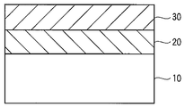
- FIG. 1 is a cross-sectional view schematically showing a basic configuration of a semiconductor device according to the first embodiment of the present invention.
- FIG. 2 is a cross-sectional view schematically showing a detailed configuration of the light emitting layer according to the first embodiment of the present invention.
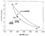
- FIG. 3 is a diagram showing the relationship between the lattice constant and the band gap.
- FIG. 4 is a diagram showing measurement results of the semiconductor device according to the first embodiment of the present invention.
- FIG. 5 is a diagram showing measurement results of the semiconductor device according to the first comparative example of the first embodiment of the present invention.
- FIG. 6 is a diagram showing measurement results of the semiconductor device according to the second comparative example of the first embodiment of the present invention.
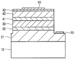
- FIG. 7 is a cross-sectional view schematically showing the configuration of the semiconductor device according to the second embodiment of the present invention.
- FIG. 1 is a cross-sectional view schematically showing a basic configuration of a semiconductor device (light emitting diode) according to a first embodiment of the present invention.
- the semiconductor device shown in FIG. 1 includes a substrate 10, a base layer 20 formed on the substrate 10, and a light emitting layer 30 formed on the base layer 20.
- a sapphire substrate is used as the substrate 10, and the upper surface (element formation surface) of the sapphire substrate 10 is a (0001) plane of a sapphire crystal, that is, a C plane.
- a GaN layer is formed as a base layer 20 on the upper surface (C surface) of the sapphire substrate 10.
- a light emitting layer 30 having a multiple quantum well structure is formed on the GaN layer 20.
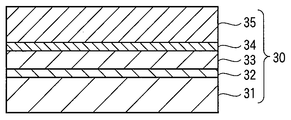
- FIG. 2 is a cross-sectional view schematically showing a detailed configuration of the light emitting layer 30 shown in FIG.
- the light emitting layer 30 has a stacked structure of a barrier layer (barrier layer) 31, an intermediate layer 32, a quantum well layer 33, an intermediate layer 34, and a barrier layer (barrier layer) 35.
- the barrier layer 31 InAlGaN (generally, In x Al y Ga 1- xy N (0 ⁇ x ⁇ 1,0 ⁇ denoted y ⁇ 1)) is formed, the thickness 12. 5 nm. Specifically, the barrier layer 31 is made of In 0.02 Al 0.33 Ga 0.65 N.
- the intermediate layer 32 is made of InGaN (generally expressed as In x Ga 1-x N (0 ⁇ x ⁇ 1)) and has a thickness of 0.5 nm. Specifically, the intermediate layer 32 is formed of In 0.02 Ga 0.98 N.
- the quantum well layer 33 is made of InGaN (generally expressed as In x Ga 1-x N (0 ⁇ x ⁇ 1)) and has a thickness of 2.5 nm. Specifically, the quantum well layer 33 is formed of In 0.15 Ga 0.85 N.
- the intermediate layer 34 is made of InGaN (generally expressed as In x Ga 1-x N (0 ⁇ x ⁇ 1)) and has a thickness of 0.5 nm. Specifically, the intermediate layer 34 is formed of In 0.02 Ga 0.98 N.
- the barrier layer 35 is made of InAlGaN (generally, In x Al y Ga 1-xy N (represented as 0 ⁇ x ⁇ 1, 0 ⁇ y ⁇ 1)) and has a thickness of 11. 5 nm. Specifically, the barrier layer 35 is made of In 0.02 Al 0.33 Ga 0.65 N.
- the laminated structure of FIG. 2 is formed for five periods.
- the top layer as a cap layer
- the thickness is 15 nm InAlGaN of (in general, expressed as In x Al y Ga 1-xy N (0 ⁇ x ⁇ 1,0 ⁇ y ⁇ 1))
- a layer is formed.
- the cap layer is formed of In 0.02 Al 0.33 Ga 0.65 N.
- the above-described structure is formed by epitaxially growing the base layer 20 and the light emitting layer 30 on the substantially (0001) plane (that is, the C plane) of the sapphire substrate 10.
- a metal organic chemical vapor deposition (MOCVD) method, a molecular beam epitaxy (MBE) method, or the like can be used as the epitaxial growth method.
- FIG. 3 is a diagram showing the relationship between the lattice constant and the band gap (forbidden band width) in a compound semiconductor.
- InGaN has a larger lattice constant than GaN, and the lattice constant of InGaN increases as the In composition of InGaN increases. Therefore, when an InGaN layer having a high In composition such as a quantum well layer is grown on the GaN layer, compressive strain occurs in the plane direction (a-axis direction), and tensile strain occurs in the growth direction (c-axis direction). Arise. In this case, by providing an InGaN layer with a low In composition or an InAlGaN layer with a low In composition as the barrier layer, the compressive strain in the plane direction (a-axis direction) can be reduced.
- the tensile strain in the growth direction cannot be greatly relieved. If the tensile strain in the c-axis direction is large, the piezoelectric field due to piezoelectric polarization increases. Therefore, the recombination probability of electrons and holes is lowered, and the light emission efficiency is lowered.
- the piezo electric field due to tensile strain in the c-axis direction increases as the In composition increases. Further, when the piezoelectric field is large, the dependence of the quantum efficiency on the injection current density is examined, and the quantum efficiency is significantly lowered in the high injection current density region.
- the In composition of the quantum well layer is increased, the light emission efficiency is lowered.
- the In composition of the quantum well layer in order to increase the emission wavelength (decrease the band gap), it is necessary to increase the In composition of the quantum well layer. From the above, when an InGaN layer having a low In composition is used as the barrier layer, it is difficult to increase the emission wavelength without significantly reducing the light emission efficiency.
- the barrier layer when an InAlGaN layer having a low In composition is used as the barrier layer, the tensile strain in the growth direction (c-axis direction) can be greatly reduced. Therefore, even if the In composition of the quantum well layer is increased in order to increase the emission wavelength, it is possible to suppress a significant decrease in light emission efficiency. Therefore, as in this embodiment, by using an InAlGaN layer as the barrier layer, it is possible to increase the emission wavelength without significantly reducing the emission efficiency. In addition, since the piezo electric field can be reduced in this embodiment, it is possible to suppress a decrease in quantum efficiency in a high injection current density region, and it is possible to provide a light emitting diode with high injection current density and high efficiency. is there.
- the band gap energy of the barrier layer is increased, and overflow of carriers, particularly electrons, can be suppressed. Therefore, it is optimal for a light emitting diode used at a high injection current density. For example, a high power light emitting diode having a current density of about 100 A / cm 2 or more can be obtained.
- the emission wavelength can be increased. From this point of view as well, in the present embodiment, it is possible to increase the emission wavelength without significantly reducing the light emission efficiency. In other words, when producing light emitting diodes having the same emission wavelength, the In composition of the quantum well layer can be lowered in this embodiment. A description will be added below. Originally, if the In composition of the InGaN quantum well layer is the same, the emission wavelength should not change.
- the reason why the emission wavelength can be increased by using the InAlGaN layer as the barrier layer is thought to be as follows.
- the band gap difference and the lattice constant difference between AlN and InN are larger than those between GaN and InN. Therefore, when an InAlGaN layer is used as the barrier layer, thermodynamic compositional modulation is likely to occur. Therefore, it is considered that an InGaN layer having a high In composition is locally formed and the emission wavelength can be increased. Since the In composition of the quantum well layer can be lowered, thermodynamic compositional modulation is suppressed, and the crystal becomes thermodynamically stable, so that a highly reliable semiconductor device can be provided. In addition, since the In composition of the quantum well layer can be reduced, the thickness of the quantum well layer can be increased and the current density per quantum well layer can be reduced.
- the InAlGaN layer as the barrier layer, it is possible to increase the emission wavelength without significantly reducing the emission efficiency. As a result, it is possible to obtain green light with high luminous efficiency, which has been difficult in the past.
- an intermediate layer 32 is provided between the barrier layer 31 and the quantum well layer 33, and an intermediate layer 34 is provided between the barrier layer 35 and the quantum well layer 33.
- the difference in lattice constant between AlN and InN is large.
- the Al composition of the InAlGaN barrier layer is high to some extent
- the In composition of the InGaN quantum well layer is high to some extent. Therefore, when an InAlGaN barrier layer and an InGaN quantum well layer are stacked without an intermediate layer, a situation where AlN of the barrier layer and InN of the quantum well layer are in direct contact with each other tends to occur. As a result, a sudden lattice mismatch occurs, and phase separation and crystal defects are likely to occur near the interface between the barrier layer and the quantum well layer.
- an InGaN intermediate layer having a low In composition is interposed between the barrier layer and the quantum well layer so as not to affect the band structure. That is, in the InGaN intermediate layer, the Ga composition is much higher than the In composition, and GaN is dominant. As can be seen from FIG. 3, GaN has an intermediate lattice constant between that of AlN and that of InN. Therefore, by interposing the InGaN intermediate layer between the InAlGaN barrier layer and the InGaN quantum well layer, a sudden lattice mismatch between the barrier layer and the quantum well layer can be suppressed. As a result, the occurrence of phase separation and defects can be suppressed, and the light emission efficiency can be improved.
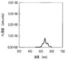
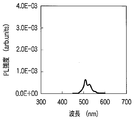
- FIG. 4 is a diagram showing measurement results of the semiconductor device (light emitting diode) according to the present embodiment. Specifically, it is the figure which showed the measurement result by microphotoluminescence (PL). As shown in FIG. 4, a green emission spectrum having a very strong emission intensity with a center wavelength of 495 nm was obtained.
- PL microphotoluminescence
- FIG. 5 is a diagram showing a measurement result of the semiconductor device (light emitting diode) according to the first comparative example of the present embodiment.
- the barrier layer is formed of InGaN, and the In composition of the quantum well layer is increased to 0.35 in order to increase the emission wavelength.
- the emission intensity is greatly reduced in the comparative example.
- the In composition of the quantum well layer is increased in order to increase the wavelength, it is considered that the light emission efficiency is greatly reduced for the reasons already described.
- FIG. 6 is a diagram showing a measurement result of the semiconductor device (light emitting diode) according to the second comparative example of the present embodiment.
- the barrier layer and the quantum well layer are stacked without providing an intermediate layer. Compared to the present embodiment, the emission intensity is greatly reduced in the comparative example.
- the barrier layer and the quantum well layer are directly stacked without using an intermediate layer, it is considered that the light emission efficiency is greatly reduced for the reasons already described.
- the Al composition of the barrier layer is preferably in the range of 0.2 to 0.4, and the In composition of the barrier layer is preferably in the range of 0.01 to 0.05.
- the film thickness of the barrier layer is preferably in the range of 4 to 20 nm.
- the intermediate layer preferably has the same In composition as the barrier layer or higher than the barrier layer.
- the In composition of the intermediate layer is preferably in the range of 0.01 to 0.05 equivalent to the In composition of the barrier layer. By doing so, a sudden lattice mismatch is suppressed, and the occurrence of phase separation and defects can be effectively suppressed.
- the In composition of the quantum well layer is preferably in the range of 0.1 to 0.3.
- the thickness of the intermediate layer is preferably in the range of 0.5 to 1.5 nm.
- FIG. 7 is a cross-sectional view schematically showing the configuration of the semiconductor device (light emitting diode) according to the present embodiment.
- a sapphire substrate is used as the substrate 10, and the upper surface (element formation surface) of the sapphire substrate 10 is a (0001) plane of a sapphire crystal, that is, a C plane.
- a p-type GaN contact layer 43 are stacked.
- An n-side electrode 50 made of Ti / Pt / Au is formed on the exposed surface of the n-type GaN contact layer 21.
- a p-side electrode 60 made of Ni / Au is formed on the surface of the p-type GaN contact layer 43.
- the structure of the light emitting layer 30 is the same as the structure described in the first embodiment.
- the overflow prevention layer is particularly effective in a high power light emitting diode having a current density of, for example, about 100 A / cm 2 or more.
- the overflow preventing layer for example, in addition to the above examples, the layer having a composition of p-In u Al v Ga 1 -uv N (0 ⁇ u ⁇ 1,0 ⁇ v ⁇ 1) and the like.
- the overflow prevention layer desirably has a higher Al composition than the barrier layer for that purpose.
- Each layer of the semiconductor device is formed by metal organic chemical vapor deposition (MOCVD).
- MOCVD metal organic chemical vapor deposition
- TMG trimethylgallium
- TMA trimethylaluminum
- TMI trimethylindium
- Cp 2 Mg biscyclopentadienylmagnesium
- ammonia NH 3
- silane SiH 4
- Hydrogen and nitrogen can be used as the carrier gas.
- a sapphire substrate treated by organic cleaning and acid cleaning is introduced into a reaction chamber of an MOCVD apparatus and placed on a susceptor heated by high frequency. Subsequently, the temperature is raised to a temperature of 1100 ° C. over about 12 minutes in a normal pressure nitrogen / hydrogen atmosphere. In the temperature rising process, vapor phase etching is performed on the substrate surface to remove the natural oxide film on the substrate surface.
- nitrogen / hydrogen is used as a carrier gas
- ammonia is supplied at 6 L / min
- TMG is supplied at 50 cc / min
- SiH 4 is supplied at a flow rate of 10 cc / min for 60 minutes to form the n-type GaN contact layer 21.
- the temperature is lowered to 1060 ° C.
- SiH 4 is lowered to 3 cc / min
- the n-type GaN guide layer 22 is formed in about 3 minutes.
- TMI is supplied at a flow rate of 5 cc / min and SiH4 at a flow rate of 1 cc / min for 2 minutes, and then TMA is further added at a flow rate of 16 cc / min for 12 minutes. Thereafter, the supply of TMA is stopped, and the growth of 2 minutes is performed with the supply of TMG and SiH 4 as they are. Thereafter, the supply amount of TMI is increased to 80 cc / min, and growth is performed for 40 seconds.
- TMG is supplied at a flow rate of 3 cc / min and TMI at a flow rate of 5 cc / min for about 14 minutes to form the light emitting layer 30 having a multiple quantum well structure.
- the flow rate of TMG, TMA, or TMI may be changed to incline the Al composition or the In composition in the barrier layer 31 or the intermediate layer 32.
- the period of the multiple quantum well structure is not limited to 5, but can be selected in the range of 2 to 10.
- the p-type AlGaN overflow prevention layer 41 is formed by supplying TMG at a flow rate of 25 cc / min, TMA at about 30 cc / min, and Cp 2 Mg at a flow rate of 6 cc / min for about 1 minute.
- the Al composition of the p-type AlGaN may be 0.2 or more, but is preferably higher than the Al composition of the InAlGaN barrier layer 31. Thereby, the overflow of electrons can be remarkably suppressed, which is particularly desirable for a semiconductor device used at a high current density.
- the supply of only TMA is stopped from the above state, and the p-type GaN layer 42 is formed by switching Cp 2 Mg to a flow rate of 8 cc / min for about 6 minutes.
- Cp 2 Mg is supplied from the above state at a flow rate of 50 cc / min for about 3 minutes to form the p-type GaN contact layer 43. Subsequently, the supply of the organometallic raw material is stopped, only the carrier gas is continuously supplied, and the substrate temperature is naturally lowered. However, the supply of ammonia is stopped when the substrate temperature reaches 500 ° C.
- n-side electrode 50 made of Ti / Pt / Au is formed on the exposed contact layer 21.
- a p-side electrode 60 made of Ni / Au is formed on the p-type GaN contact layer 43.
- a sapphire substrate is used as the substrate, but a GaN substrate, SiC substrate, ZnO substrate, or the like can also be used.
- the element formation surface is not limited to the C surface, and each layer can be formed on a nonpolar surface. It is also possible to apply a structure in which electrodes are provided on the back side of the wafer. Furthermore, it is possible to obtain not only a green light emitting diode with high luminous efficiency but also a blue light emitting diode with high luminous efficiency.
Landscapes
- Led Devices (AREA)
Abstract
Description
図1は、本発明の第1の実施形態に係る半導体装置(発光ダイオード)の基本的な構成を模式的に示した断面図である。図1に示した半導体装置は、基板10と、基板10上に形成された下地層20と、下地層20上に形成された発光層30によって構成されている。
次に、本発明の第2の実施形態について説明する。なお、基本的な構成は第1の実施形態と同様であり、第1の実施形態で説明した事項については説明を省略する。
Claims (7)
- 下地層と、
前記下地層上に形成され、InAlGaNで形成された障壁層とInGaNで形成された量子井戸層とが交互に積層された発光層と、
を備えたことを特徴とする半導体装置。 - 前記障壁層は、前記量子井戸層よりも低いIn組成を有する
ことを特徴とする請求項1に記載の半導体装置。 - 互いに隣接する前記障壁層と前記量子井戸層との間に設けられ、InGaNで形成され且つ前記量子井戸層よりも低いIn組成を有する中間層をさらに備えた
ことを特徴とする請求項2に記載の半導体装置。 - 前記発光層上に形成され、前記障壁層よりも高いAl組成を有するオーバーフロー防止層をさらに備えた
ことを特徴とする請求項3に記載の半導体装置。 - 前記発光層上に形成された、p-InuAlvGa1-u-vN(0≦u<1,0<v<1)層をさらに備えた
ことを特徴とする請求項3に記載の半導体装置。 - 前記下地層は、GaNで形成されている
ことを特徴とする請求項2に記載の半導体装置。 - 前記下地層は、基板の実質的に(0001)面上に形成されている
ことを特徴とする請求項6に記載の半導体装置。
Priority Applications (3)
| Application Number | Priority Date | Filing Date | Title |
|---|---|---|---|
| EP09810080.3A EP2325899A4 (en) | 2008-08-29 | 2009-08-31 | SEMICONDUCTOR COMPONENT |
| CN2009801334030A CN102138227A (zh) | 2008-08-29 | 2009-08-31 | 半导体装置 |
| US12/716,668 US20100187497A1 (en) | 2008-08-29 | 2010-03-03 | Semiconductor device |
Applications Claiming Priority (2)
| Application Number | Priority Date | Filing Date | Title |
|---|---|---|---|
| JP2008-221471 | 2008-08-29 | ||
| JP2008221471 | 2008-08-29 |
Related Child Applications (1)
| Application Number | Title | Priority Date | Filing Date |
|---|---|---|---|
| US12/716,668 Continuation US20100187497A1 (en) | 2008-08-29 | 2010-03-03 | Semiconductor device |
Publications (1)
| Publication Number | Publication Date |
|---|---|
| WO2010024436A1 true WO2010024436A1 (ja) | 2010-03-04 |
Family
ID=41721595
Family Applications (1)
| Application Number | Title | Priority Date | Filing Date |
|---|---|---|---|
| PCT/JP2009/065195 Ceased WO2010024436A1 (ja) | 2008-08-29 | 2009-08-31 | 半導体装置 |
Country Status (6)
| Country | Link |
|---|---|
| US (1) | US20100187497A1 (ja) |
| EP (1) | EP2325899A4 (ja) |
| JP (2) | JP2010080955A (ja) |
| KR (1) | KR20110034689A (ja) |
| CN (1) | CN102138227A (ja) |
| WO (1) | WO2010024436A1 (ja) |
Cited By (1)
| Publication number | Priority date | Publication date | Assignee | Title |
|---|---|---|---|---|
| US12027646B2 (en) | 2018-10-25 | 2024-07-02 | Nichia Corporation | Light emitting element |
Families Citing this family (26)
| Publication number | Priority date | Publication date | Assignee | Title |
|---|---|---|---|---|
| WO2011027417A1 (ja) | 2009-09-01 | 2011-03-10 | 株式会社 東芝 | 半導体発光素子 |
| JP4940317B2 (ja) * | 2010-02-25 | 2012-05-30 | 株式会社東芝 | 半導体発光素子及びその製造方法 |
| JP5325171B2 (ja) * | 2010-07-08 | 2013-10-23 | 株式会社東芝 | 半導体発光素子 |
| US9142413B2 (en) * | 2010-11-08 | 2015-09-22 | Georgia Tech Research Corporation | Methods for growing a non-phase separated group-III nitride semiconductor alloy |
| US20130082274A1 (en) * | 2011-09-29 | 2013-04-04 | Bridgelux, Inc. | Light emitting devices having dislocation density maintaining buffer layers |
| KR101262726B1 (ko) * | 2011-12-30 | 2013-05-09 | 일진엘이디(주) | 탄소 도핑된 p형 질화물층을 포함하는 질화물계 발광소자 제조 방법 |
| RU2615215C2 (ru) * | 2012-02-28 | 2017-04-04 | Конинклейке Филипс Н.В. | Интеграция светодиодов на нитриде галлия с приборами на нитриде алюминия-галлия/нитриде галлия на кремниевых подложках для светодиодов переменного тока |
| US9343626B2 (en) | 2013-03-15 | 2016-05-17 | Soitec | Semiconductor structures having active regions comprising InGaN, methods of forming such semiconductor structures, and light emitting devices formed from such semiconductor structures |
| TWI593135B (zh) | 2013-03-15 | 2017-07-21 | 索泰克公司 | 具有含氮化銦鎵之主動區域之半導體結構,形成此等半導體結構之方法,以及應用此等半導體結構形成之發光元件 |
| DE112014001385T5 (de) * | 2013-03-15 | 2015-12-17 | Soitec | Halbleiterlichtemitterstruktur mit einem aktiven Gebiet, das InGaN enthält, und Verfahren für seine Herstellung |
| FR3003397B1 (fr) * | 2013-03-15 | 2016-07-22 | Soitec Silicon On Insulator | Structures semi-conductrices dotées de régions actives comprenant de l'INGAN |
| JP5606595B2 (ja) * | 2013-06-28 | 2014-10-15 | 株式会社東芝 | 半導体発光素子の製造方法 |
| FR3012676A1 (fr) | 2013-10-25 | 2015-05-01 | Commissariat Energie Atomique | Diode electroluminescente a puits quantiques separes par des couches barrieres d'ingan a compositions d'indium variables |
| JP6281469B2 (ja) * | 2014-11-03 | 2018-02-21 | 豊田合成株式会社 | 発光素子の製造方法 |
| US9985168B1 (en) | 2014-11-18 | 2018-05-29 | Cree, Inc. | Group III nitride based LED structures including multiple quantum wells with barrier-well unit interface layers |
| EP3255119B1 (en) * | 2015-02-02 | 2019-11-13 | Stanley Electric Co., Ltd. | Method for manufacturing quantum dot |
| JP6764230B2 (ja) * | 2015-02-06 | 2020-09-30 | スタンレー電気株式会社 | 半導体ナノ粒子の製造方法 |
| JP6764231B2 (ja) * | 2015-02-06 | 2020-09-30 | スタンレー電気株式会社 | 半導体ナノ粒子の製造方法、および、半導体ナノ粒子 |
| JP6128138B2 (ja) * | 2015-02-10 | 2017-05-17 | ウシオ電機株式会社 | 半導体発光素子 |
| DE102016116425B4 (de) | 2016-09-02 | 2026-04-23 | OSRAM Opto Semiconductors Gesellschaft mit beschränkter Haftung | Optoelektronisches Bauelement |
| US11393948B2 (en) | 2018-08-31 | 2022-07-19 | Creeled, Inc. | Group III nitride LED structures with improved electrical performance |
| US11404473B2 (en) | 2019-12-23 | 2022-08-02 | Lumileds Llc | III-nitride multi-wavelength LED arrays |
| US11923398B2 (en) | 2019-12-23 | 2024-03-05 | Lumileds Llc | III-nitride multi-wavelength LED arrays |
| TWI912314B (zh) | 2020-05-04 | 2026-01-21 | 美商谷歌有限責任公司 | 顯示器、發光二極體結構及用於形成其之相關聯的方法 |
| US11631786B2 (en) * | 2020-11-12 | 2023-04-18 | Lumileds Llc | III-nitride multi-wavelength LED arrays with etch stop layer |
| CN115458649B (zh) * | 2022-10-21 | 2025-05-02 | 江西兆驰半导体有限公司 | 发光二极管外延片及其制备方法、发光二极管 |
Citations (9)
| Publication number | Priority date | Publication date | Assignee | Title |
|---|---|---|---|---|
| JPH1065271A (ja) * | 1996-08-13 | 1998-03-06 | Toshiba Corp | 窒化ガリウム系半導体光発光素子 |
| JPH1084132A (ja) * | 1996-09-08 | 1998-03-31 | Toyoda Gosei Co Ltd | 半導体発光素子 |
| JPH10270756A (ja) * | 1997-03-27 | 1998-10-09 | Sanyo Electric Co Ltd | 窒化ガリウム系化合物半導体装置 |
| JP2000232259A (ja) * | 1998-12-09 | 2000-08-22 | Sanyo Electric Co Ltd | 発光素子及びその製造方法 |
| JP2002043618A (ja) | 2000-07-21 | 2002-02-08 | Matsushita Electric Ind Co Ltd | 窒化物半導体の製造方法 |
| JP2003115642A (ja) * | 2001-03-28 | 2003-04-18 | Nichia Chem Ind Ltd | 窒化物半導体素子 |
| WO2004008551A1 (ja) * | 2002-07-16 | 2004-01-22 | Nitride Semiconductors Co.,Ltd. | 窒化ガリウム系化合物半導体装置 |
| JP2004200347A (ja) * | 2002-12-18 | 2004-07-15 | Sumitomo Electric Ind Ltd | 高放熱性能を持つ発光ダイオード |
| JP2007214221A (ja) * | 2006-02-08 | 2007-08-23 | Sharp Corp | 窒化物半導体レーザ素子 |
Family Cites Families (10)
| Publication number | Priority date | Publication date | Assignee | Title |
|---|---|---|---|---|
| US5684309A (en) * | 1996-07-11 | 1997-11-04 | North Carolina State University | Stacked quantum well aluminum indium gallium nitride light emitting diodes |
| JP4032636B2 (ja) * | 1999-12-13 | 2008-01-16 | 日亜化学工業株式会社 | 発光素子 |
| KR100906760B1 (ko) * | 2001-03-28 | 2009-07-09 | 니치아 카가쿠 고교 가부시키가이샤 | 질화물 반도체 소자 |
| US20040161006A1 (en) * | 2003-02-18 | 2004-08-19 | Ying-Lan Chang | Method and apparatus for improving wavelength stability for InGaAsN devices |
| JP4412918B2 (ja) * | 2003-05-28 | 2010-02-10 | シャープ株式会社 | 窒化物半導体発光素子及びその製造方法 |
| JP2004015072A (ja) * | 2003-09-26 | 2004-01-15 | Nichia Chem Ind Ltd | 窒化物半導体発光素子 |
| JP4389723B2 (ja) * | 2004-02-17 | 2009-12-24 | 住友電気工業株式会社 | 半導体素子を形成する方法 |
| CN100349306C (zh) * | 2004-08-27 | 2007-11-14 | 中国科学院半导体研究所 | 蓝光、黄光量子阱堆叠结构白光发光二极管及制作方法 |
| JP2007088270A (ja) * | 2005-09-22 | 2007-04-05 | Matsushita Electric Works Ltd | 半導体発光素子およびそれを用いる照明装置ならびに半導体発光素子の製造方法 |
| KR100753518B1 (ko) * | 2006-05-23 | 2007-08-31 | 엘지전자 주식회사 | 질화물계 발광 소자 |
-
2009
- 2009-08-31 EP EP09810080.3A patent/EP2325899A4/en not_active Withdrawn
- 2009-08-31 CN CN2009801334030A patent/CN102138227A/zh active Pending
- 2009-08-31 JP JP2009201071A patent/JP2010080955A/ja active Pending
- 2009-08-31 KR KR1020117004435A patent/KR20110034689A/ko not_active Ceased
- 2009-08-31 WO PCT/JP2009/065195 patent/WO2010024436A1/ja not_active Ceased
-
2010
- 2010-03-03 US US12/716,668 patent/US20100187497A1/en not_active Abandoned
-
2011
- 2011-09-26 JP JP2011209882A patent/JP5634368B2/ja active Active
Patent Citations (9)
| Publication number | Priority date | Publication date | Assignee | Title |
|---|---|---|---|---|
| JPH1065271A (ja) * | 1996-08-13 | 1998-03-06 | Toshiba Corp | 窒化ガリウム系半導体光発光素子 |
| JPH1084132A (ja) * | 1996-09-08 | 1998-03-31 | Toyoda Gosei Co Ltd | 半導体発光素子 |
| JPH10270756A (ja) * | 1997-03-27 | 1998-10-09 | Sanyo Electric Co Ltd | 窒化ガリウム系化合物半導体装置 |
| JP2000232259A (ja) * | 1998-12-09 | 2000-08-22 | Sanyo Electric Co Ltd | 発光素子及びその製造方法 |
| JP2002043618A (ja) | 2000-07-21 | 2002-02-08 | Matsushita Electric Ind Co Ltd | 窒化物半導体の製造方法 |
| JP2003115642A (ja) * | 2001-03-28 | 2003-04-18 | Nichia Chem Ind Ltd | 窒化物半導体素子 |
| WO2004008551A1 (ja) * | 2002-07-16 | 2004-01-22 | Nitride Semiconductors Co.,Ltd. | 窒化ガリウム系化合物半導体装置 |
| JP2004200347A (ja) * | 2002-12-18 | 2004-07-15 | Sumitomo Electric Ind Ltd | 高放熱性能を持つ発光ダイオード |
| JP2007214221A (ja) * | 2006-02-08 | 2007-08-23 | Sharp Corp | 窒化物半導体レーザ素子 |
Non-Patent Citations (1)
| Title |
|---|
| See also references of EP2325899A4 |
Cited By (1)
| Publication number | Priority date | Publication date | Assignee | Title |
|---|---|---|---|---|
| US12027646B2 (en) | 2018-10-25 | 2024-07-02 | Nichia Corporation | Light emitting element |
Also Published As
| Publication number | Publication date |
|---|---|
| JP5634368B2 (ja) | 2014-12-03 |
| JP2011258994A (ja) | 2011-12-22 |
| US20100187497A1 (en) | 2010-07-29 |
| CN102138227A (zh) | 2011-07-27 |
| EP2325899A4 (en) | 2015-04-29 |
| KR20110034689A (ko) | 2011-04-05 |
| JP2010080955A (ja) | 2010-04-08 |
| EP2325899A1 (en) | 2011-05-25 |
Similar Documents
| Publication | Publication Date | Title |
|---|---|---|
| JP5634368B2 (ja) | 半導体装置 | |
| CN101689586B (zh) | 氮化物半导体发光元件和氮化物半导体的制造方法 | |
| KR101399250B1 (ko) | 질소 화합물 반도체 발광 소자 및 그 제조 방법 | |
| US8716048B2 (en) | Light emitting device and method for manufacturing the same | |
| US9755107B2 (en) | Group III nitride semiconductor light-emitting device | |
| JP2021015952A (ja) | 紫外線led及びその製造方法 | |
| US20110042713A1 (en) | Nitride semi-conductive light emitting device | |
| JP2008288397A (ja) | 半導体発光装置 | |
| WO2015146069A1 (ja) | 発光ダイオード素子 | |
| JP5048236B2 (ja) | 半導体発光素子、および半導体発光素子を作製する方法 | |
| CN110289343A (zh) | 一种非极性面氮化镓衬底外延结构及其制备方法与应用 | |
| KR100998234B1 (ko) | 질화물 반도체 발광 소자 및 그 제조 방법 | |
| JP2004014587A (ja) | 窒化物系化合物半導体エピタキシャルウエハ及び発光素子 | |
| US9564552B2 (en) | Method for producing group III nitride semiconductor light-emitting device | |
| CN104112799A (zh) | 一种晶格匹配的led外延结构及其制备方法 | |
| US9595633B2 (en) | Method for producing light-emitting device and method for producing group III nitride semiconductor | |
| US9508895B2 (en) | Group III nitride semiconductor light-emitting device and production method therefor | |
| JP2011223043A (ja) | 半導体発光素子、および半導体発光素子を作製する方法 | |
| JP5340351B2 (ja) | 窒化物半導体装置 | |
| KR20120131147A (ko) | 발광 소자 및 그 제조 방법 | |
| KR20090102204A (ko) | 발광 소자 및 그 제조 방법 | |
| JP2000294829A (ja) | 半導体積層構造とそれを備えた半導体素子及び結晶成長方法 | |
| JP2016111079A (ja) | 半導体発光素子 | |
| KR20100109166A (ko) | 인듐을 포함하는 질화물계 반도체층을 가지는 발광 다이오드 |
Legal Events
| Date | Code | Title | Description |
|---|---|---|---|
| WWE | Wipo information: entry into national phase |
Ref document number: 200980133403.0 Country of ref document: CN |
|
| 121 | Ep: the epo has been informed by wipo that ep was designated in this application |
Ref document number: 09810080 Country of ref document: EP Kind code of ref document: A1 |
|
| WWE | Wipo information: entry into national phase |
Ref document number: 2009810080 Country of ref document: EP |
|
| ENP | Entry into the national phase |
Ref document number: 20117004435 Country of ref document: KR Kind code of ref document: A |
|
| NENP | Non-entry into the national phase |
Ref country code: DE |