WO2010052982A1 - Procédé de production de dispositif de conversion photoélectrique et dispositif de conversion photoélectrique - Google Patents
Procédé de production de dispositif de conversion photoélectrique et dispositif de conversion photoélectrique Download PDFInfo
- Publication number
- WO2010052982A1 WO2010052982A1 PCT/JP2009/067250 JP2009067250W WO2010052982A1 WO 2010052982 A1 WO2010052982 A1 WO 2010052982A1 JP 2009067250 W JP2009067250 W JP 2009067250W WO 2010052982 A1 WO2010052982 A1 WO 2010052982A1
- Authority
- WO
- WIPO (PCT)
- Prior art keywords
- layer
- intermediate contact
- contact layer
- photoelectric conversion
- separation
- Prior art date
- Legal status (The legal status is an assumption and is not a legal conclusion. Google has not performed a legal analysis and makes no representation as to the accuracy of the status listed.)
- Ceased
Links
Images




Classifications
-
- H—ELECTRICITY
- H10—SEMICONDUCTOR DEVICES; ELECTRIC SOLID-STATE DEVICES NOT OTHERWISE PROVIDED FOR
- H10F—INORGANIC SEMICONDUCTOR DEVICES SENSITIVE TO INFRARED RADIATION, LIGHT, ELECTROMAGNETIC RADIATION OF SHORTER WAVELENGTH OR CORPUSCULAR RADIATION
- H10F71/00—Manufacture or treatment of devices covered by this subclass
- H10F71/121—The active layers comprising only Group IV materials
-
- H—ELECTRICITY
- H10—SEMICONDUCTOR DEVICES; ELECTRIC SOLID-STATE DEVICES NOT OTHERWISE PROVIDED FOR
- H10F—INORGANIC SEMICONDUCTOR DEVICES SENSITIVE TO INFRARED RADIATION, LIGHT, ELECTROMAGNETIC RADIATION OF SHORTER WAVELENGTH OR CORPUSCULAR RADIATION
- H10F10/00—Individual photovoltaic cells, e.g. solar cells
-
- H—ELECTRICITY
- H10—SEMICONDUCTOR DEVICES; ELECTRIC SOLID-STATE DEVICES NOT OTHERWISE PROVIDED FOR
- H10F—INORGANIC SEMICONDUCTOR DEVICES SENSITIVE TO INFRARED RADIATION, LIGHT, ELECTROMAGNETIC RADIATION OF SHORTER WAVELENGTH OR CORPUSCULAR RADIATION
- H10F10/00—Individual photovoltaic cells, e.g. solar cells
- H10F10/10—Individual photovoltaic cells, e.g. solar cells having potential barriers
- H10F10/17—Photovoltaic cells having only PIN junction potential barriers
- H10F10/174—Photovoltaic cells having only PIN junction potential barriers comprising monocrystalline or polycrystalline materials
-
- H—ELECTRICITY
- H10—SEMICONDUCTOR DEVICES; ELECTRIC SOLID-STATE DEVICES NOT OTHERWISE PROVIDED FOR
- H10F—INORGANIC SEMICONDUCTOR DEVICES SENSITIVE TO INFRARED RADIATION, LIGHT, ELECTROMAGNETIC RADIATION OF SHORTER WAVELENGTH OR CORPUSCULAR RADIATION
- H10F71/00—Manufacture or treatment of devices covered by this subclass
-
- H—ELECTRICITY
- H10—SEMICONDUCTOR DEVICES; ELECTRIC SOLID-STATE DEVICES NOT OTHERWISE PROVIDED FOR
- H10F—INORGANIC SEMICONDUCTOR DEVICES SENSITIVE TO INFRARED RADIATION, LIGHT, ELECTROMAGNETIC RADIATION OF SHORTER WAVELENGTH OR CORPUSCULAR RADIATION
- H10F71/00—Manufacture or treatment of devices covered by this subclass
- H10F71/10—Manufacture or treatment of devices covered by this subclass the devices comprising amorphous semiconductor material
- H10F71/103—Manufacture or treatment of devices covered by this subclass the devices comprising amorphous semiconductor material including only Group IV materials
-
- H—ELECTRICITY
- H10—SEMICONDUCTOR DEVICES; ELECTRIC SOLID-STATE DEVICES NOT OTHERWISE PROVIDED FOR
- H10F—INORGANIC SEMICONDUCTOR DEVICES SENSITIVE TO INFRARED RADIATION, LIGHT, ELECTROMAGNETIC RADIATION OF SHORTER WAVELENGTH OR CORPUSCULAR RADIATION
- H10F71/00—Manufacture or treatment of devices covered by this subclass
- H10F71/121—The active layers comprising only Group IV materials
- H10F71/1221—The active layers comprising only Group IV materials comprising polycrystalline silicon
-
- H—ELECTRICITY
- H10—SEMICONDUCTOR DEVICES; ELECTRIC SOLID-STATE DEVICES NOT OTHERWISE PROVIDED FOR
- H10F—INORGANIC SEMICONDUCTOR DEVICES SENSITIVE TO INFRARED RADIATION, LIGHT, ELECTROMAGNETIC RADIATION OF SHORTER WAVELENGTH OR CORPUSCULAR RADIATION
- H10F71/00—Manufacture or treatment of devices covered by this subclass
- H10F71/121—The active layers comprising only Group IV materials
- H10F71/1224—The active layers comprising only Group IV materials comprising microcrystalline silicon
-
- H—ELECTRICITY
- H10—SEMICONDUCTOR DEVICES; ELECTRIC SOLID-STATE DEVICES NOT OTHERWISE PROVIDED FOR
- H10F—INORGANIC SEMICONDUCTOR DEVICES SENSITIVE TO INFRARED RADIATION, LIGHT, ELECTROMAGNETIC RADIATION OF SHORTER WAVELENGTH OR CORPUSCULAR RADIATION
- H10F77/00—Constructional details of devices covered by this subclass
- H10F77/10—Semiconductor bodies
- H10F77/16—Material structures, e.g. crystalline structures, film structures or crystal plane orientations
- H10F77/169—Thin semiconductor films on metallic or insulating substrates
- H10F77/1692—Thin semiconductor films on metallic or insulating substrates the films including only Group IV materials
-
- Y—GENERAL TAGGING OF NEW TECHNOLOGICAL DEVELOPMENTS; GENERAL TAGGING OF CROSS-SECTIONAL TECHNOLOGIES SPANNING OVER SEVERAL SECTIONS OF THE IPC; TECHNICAL SUBJECTS COVERED BY FORMER USPC CROSS-REFERENCE ART COLLECTIONS [XRACs] AND DIGESTS
- Y02—TECHNOLOGIES OR APPLICATIONS FOR MITIGATION OR ADAPTATION AGAINST CLIMATE CHANGE
- Y02E—REDUCTION OF GREENHOUSE GAS [GHG] EMISSIONS, RELATED TO ENERGY GENERATION, TRANSMISSION OR DISTRIBUTION
- Y02E10/00—Energy generation through renewable energy sources
- Y02E10/50—Photovoltaic [PV] energy
- Y02E10/545—Microcrystalline silicon PV cells
-
- Y—GENERAL TAGGING OF NEW TECHNOLOGICAL DEVELOPMENTS; GENERAL TAGGING OF CROSS-SECTIONAL TECHNOLOGIES SPANNING OVER SEVERAL SECTIONS OF THE IPC; TECHNICAL SUBJECTS COVERED BY FORMER USPC CROSS-REFERENCE ART COLLECTIONS [XRACs] AND DIGESTS
- Y02—TECHNOLOGIES OR APPLICATIONS FOR MITIGATION OR ADAPTATION AGAINST CLIMATE CHANGE
- Y02E—REDUCTION OF GREENHOUSE GAS [GHG] EMISSIONS, RELATED TO ENERGY GENERATION, TRANSMISSION OR DISTRIBUTION
- Y02E10/00—Energy generation through renewable energy sources
- Y02E10/50—Photovoltaic [PV] energy
- Y02E10/546—Polycrystalline silicon PV cells
-
- Y—GENERAL TAGGING OF NEW TECHNOLOGICAL DEVELOPMENTS; GENERAL TAGGING OF CROSS-SECTIONAL TECHNOLOGIES SPANNING OVER SEVERAL SECTIONS OF THE IPC; TECHNICAL SUBJECTS COVERED BY FORMER USPC CROSS-REFERENCE ART COLLECTIONS [XRACs] AND DIGESTS
- Y02—TECHNOLOGIES OR APPLICATIONS FOR MITIGATION OR ADAPTATION AGAINST CLIMATE CHANGE
- Y02E—REDUCTION OF GREENHOUSE GAS [GHG] EMISSIONS, RELATED TO ENERGY GENERATION, TRANSMISSION OR DISTRIBUTION
- Y02E10/00—Energy generation through renewable energy sources
- Y02E10/50—Photovoltaic [PV] energy
- Y02E10/547—Monocrystalline silicon PV cells
-
- Y—GENERAL TAGGING OF NEW TECHNOLOGICAL DEVELOPMENTS; GENERAL TAGGING OF CROSS-SECTIONAL TECHNOLOGIES SPANNING OVER SEVERAL SECTIONS OF THE IPC; TECHNICAL SUBJECTS COVERED BY FORMER USPC CROSS-REFERENCE ART COLLECTIONS [XRACs] AND DIGESTS
- Y02—TECHNOLOGIES OR APPLICATIONS FOR MITIGATION OR ADAPTATION AGAINST CLIMATE CHANGE
- Y02E—REDUCTION OF GREENHOUSE GAS [GHG] EMISSIONS, RELATED TO ENERGY GENERATION, TRANSMISSION OR DISTRIBUTION
- Y02E10/00—Energy generation through renewable energy sources
- Y02E10/50—Photovoltaic [PV] energy
- Y02E10/548—Amorphous silicon PV cells
-
- Y—GENERAL TAGGING OF NEW TECHNOLOGICAL DEVELOPMENTS; GENERAL TAGGING OF CROSS-SECTIONAL TECHNOLOGIES SPANNING OVER SEVERAL SECTIONS OF THE IPC; TECHNICAL SUBJECTS COVERED BY FORMER USPC CROSS-REFERENCE ART COLLECTIONS [XRACs] AND DIGESTS
- Y02—TECHNOLOGIES OR APPLICATIONS FOR MITIGATION OR ADAPTATION AGAINST CLIMATE CHANGE
- Y02P—CLIMATE CHANGE MITIGATION TECHNOLOGIES IN THE PRODUCTION OR PROCESSING OF GOODS
- Y02P70/00—Climate change mitigation technologies in the production process for final industrial or consumer products
- Y02P70/50—Manufacturing or production processes characterised by the final manufactured product
Definitions
- the present invention relates to a method for manufacturing a photoelectric conversion device and a photoelectric conversion device, for example, a thin film solar cell, and more particularly to a method for manufacturing a photoelectric conversion device having a step in which an intermediate contact layer is separated by a pulse laser.
- a structure in which a plurality of photoelectric conversion layers are stacked is known.
- a tandem solar cell in which an amorphous silicon layer and a microcrystalline silicon layer are stacked is known.
- This tandem solar cell is formed by sequentially laminating a transparent electrode, an amorphous silicon layer, a microcrystalline silicon layer, and a back electrode on a light transmissive substrate.
- a technique is known in which an intermediate contact layer electrically and optically connected is provided between the amorphous silicon layer and the microcrystalline silicon layer, and a part of incident light is reflected to further improve the photoelectric conversion efficiency. ing.
- a high voltage is obtained by obtaining a desired voltage by connecting a plurality of photoelectric conversion cells in series.
- a connection groove that penetrates the amorphous silicon layer, the intermediate contact layer, and the microcrystalline silicon layer is formed, and the back electrode is filled in the connection groove, Connect the transparent electrode.
- the intermediate contact layer has conductivity, when it is electrically connected to the connection groove filled with the back electrode, the current generated in the amorphous silicon layer or the microcrystalline silicon layer passes through the intermediate contact layer. Leaks into the connection groove.
- a technique for preventing current leakage from the intermediate contact layer to the connection groove by separating the intermediate contact layer by laser processing has been proposed (see Patent Documents 1 and 2).
- the present invention has been made in view of such circumstances, and a photoelectric conversion device manufacturing method and photoelectric device that prevent current leakage from the intermediate contact layer as much as possible through the intermediate contact layer separation groove
- An object is to provide a conversion device.
- the method for manufacturing a photoelectric conversion device and the photoelectric conversion device of the present invention employ the following means. That is, the method for manufacturing a photoelectric conversion device according to one embodiment of the present invention includes a first photoelectric conversion layer forming step of forming a first photoelectric conversion layer containing silicon as a main component, and on the first photoelectric conversion layer.
- An intermediate contact layer forming step for forming an intermediate contact layer electrically and optically connected to the first photoelectric conversion layer; and laser irradiation to remove the intermediate contact layer, and Forming an intermediate contact layer separation groove reaching the first photoelectric conversion layer to separate the intermediate contact layer; and the intermediate contact layer on the intermediate contact layer and in the intermediate contact layer separation groove
- a second photoelectric conversion layer forming step of forming a second photoelectric conversion layer having silicon as a main component while being electrically and optically connected to the substrate.
- the pulse width is performed by a pulsed laser that is less 750ps than 10 ps.
- the intermediate contact layer and the first photoelectric conversion layer are melted and scattered by the thermal energy given by the laser irradiation, and a groove is formed in the laser irradiation portion. Thereby, an intermediate contact layer separation groove for separating the intermediate contact layer is formed.
- the pulse width of the pulse laser used for separating the intermediate contact layer is set to 10 ps or more and 750 ps or less, which is significantly shorter than the conventional pulse width of nanoseconds, and is applied to the first photoelectric conversion layer. The time interval of the generated heat energy was made extremely short.
- the first photoelectric conversion layer is melted and scattered at an extremely short time interval as compared with a laser having a pulse width of nanoseconds, so that excessive heat is taken away from the wall portion forming the intermediate contact layer separation groove. There is nothing. Therefore, the region where silicon is recrystallized at the wall portion forming the intermediate contact layer separation groove can be made as small as possible. Thus, since the region where the resistance of silicon is recrystallized and reduced in resistance can be reduced, the current leaking through the intermediate contact layer isolation trench can be reduced.
- An amorphous silicon layer is preferably used as the first photoelectric conversion layer, and a microcrystalline silicon layer is used as the second photoelectric conversion layer.
- GZO Ga-doped ZnO
- the intermediate contact layer separation groove is terminated at a midway position of the first photoelectric conversion layer.
- the intermediate contact layer separation groove is terminated at an intermediate position of the first photoelectric conversion layer, and does not reach the electrode (or other intermediate contact layer) connected to the first photoelectric conversion layer.
- the end position of the intermediate contact layer separation groove is preferably a position where the recrystallization region does not contact the electrode (or other intermediate contact layer) connected to the first photoelectric conversion layer.
- the intermediate contact layer separation step includes a step of partially overlapping a plurality of separation holes to form a series of intermediate contact layer separation grooves.
- the overlapping width of the separation holes to be matched is set to 0% or more and 5% or less of the diameter of the separation holes.
- the pulse laser has a pulse width of 10 ps or more and 750 ps or less, thermal energy can be applied to the first photoelectric conversion layer at an extremely short time interval.
- the thermal diffusion that is absorbed and diffused by the first light energy can be suppressed to be small, so that the intermediate contact layer separation groove is formed.
- Sufficient heat energy can be input to the vicinity of the wall portion to be formed, and energy can be used without waste in the groove processing, and the separation hole formed at a desired depth can be formed to the vicinity of the periphery of the separation hole. Therefore, the overlapping width of adjacent separation holes can be reduced to 0% or more and 5% or less of the separation hole diameter, and the processing speed can be increased.
- the overlapping width of adjacent separation holes being 0% means that adjacent separation holes are in contact.
- a photoelectric conversion device includes a first photoelectric conversion layer containing silicon as a main component, an intermediate contact layer electrically and optically connected to the first photoelectric conversion layer, and the intermediate A second photoelectric conversion layer mainly composed of silicon and electrically connected to the contact layer, penetrating the intermediate contact layer so as to separate the intermediate contact layer, and the second photoelectric conversion layer.
- the intermediate contact layer separation groove reaching one photoelectric conversion layer is formed
- the intermediate contact layer separation groove is a series of grooves formed by overlapping a plurality of separation holes, and is adjacent to each other. The overlapping width of the separation holes is 0% or more and 5% or less of the diameter of the separation holes.
- the processing speed can be increased.
- the overlapping width of adjacent separation holes being 0% means that adjacent separation holes are in contact.
- the intermediate contact layer separation groove when the intermediate contact layer separation groove is processed, a pulse laser having a pulse width of 10 ps or more and 750 ps or less is used. Therefore, the silicon generated in the vicinity of the wall portion forming the intermediate contact layer separation groove is used. The recrystallization region can be limited as much as possible, and the current leaking through the intermediate separation groove can be suppressed. Thereby, the efficiency improvement of a photoelectric conversion apparatus is implement
- nanosecond pulse laser concerning the comparative example of this invention Comprising: It is the top view which showed the overlapping state of the separation hole. It is the case where the nanosecond pulse laser concerning the comparative example of this invention is used, Comprising: It is the graph which showed the energy density used for the groove
- FIG. 1 shows a longitudinal section of a tandem silicon thin film solar cell (photoelectric conversion device).
- the solar cell 10 includes a glass substrate (translucent substrate) 1, a transparent electrode layer 2, a top layer (first photoelectric conversion layer) 91, an intermediate contact layer 93, and a bottom layer (second photoelectric conversion layer) 92. And a back electrode layer 4.
- the top layer 91 is a photoelectric conversion layer mainly including an amorphous silicon-based semiconductor
- the bottom layer 92 is a photoelectric conversion layer mainly including a crystalline silicon-based semiconductor.
- silicon-based is a generic name including silicon (Si), silicon carbide (SiC), and silicon germanium (SiGe).
- Crystalstalline silicon means amorphous silicon, that is, silicon other than amorphous silicon, and includes microcrystalline silicon and polycrystalline silicon.
- the solar cell 10 of the present embodiment having the above-described configuration is manufactured as follows.
- the glass substrate soda float glass having an area of 1 m 2 or more is used. Specifically, a size of 1.4 m ⁇ 1.1 m and a thickness of 3.5 to 4.5 mm is used.
- the end face of the glass substrate 1 is preferably subjected to corner chamfering or R chamfering in order to prevent damage due to thermal stress or impact.
- a transparent electrode film mainly composed of a tin oxide film (SnO 2 ) is preferably used as the transparent electrode layer 2.
- This transparent electrode film has a thickness of about 500 nm to 800 nm, and can be obtained by film formation at about 500 ° C. using a thermal CVD apparatus. During this film forming process, a texture with appropriate irregularities is formed on the surface of the transparent electrode film.
- an alkali barrier film (not shown) may be interposed between the transparent electrode film and the substrate 1.
- the alkali barrier film is a silicon oxide film (SiO 2 ) having a thickness of, for example, 50 nm to 150 nm, and is obtained by performing a film forming process at about 500 ° C. with a thermal CVD apparatus.
- the glass substrate 1 is placed on an XY table, and the first harmonic (1064 nm) of the YAG laser is irradiated from the film surface side (upper side in the drawing) of the transparent electrode layer 2.
- the laser power is adjusted so as to be appropriate for the processing speed, and the glass substrate 1 and the laser beam are placed in a direction perpendicular to the series connection direction of the power generation cells 5 in the transparent electrode layer 2 (perpendicular to the drawing in the drawing) Are moved relative to each other to form the transparent electrode separation groove 12.
- the transparent electrode layer 2 is laser-etched into a strip shape having a predetermined width of about 6 mm to 15 mm.
- a p-layer film / i-layer film / n-layer film made of an amorphous silicon thin film is sequentially formed under the conditions of a reduced pressure atmosphere of 30 to 1000 Pa and a substrate temperature of about 200 ° C.
- the top layer 91 is formed (first photoelectric conversion layer forming step).
- the top layer 91 is formed on the transparent electrode layer 2 by a process gas using SiH 4 gas and H 2 gas as main raw materials.
- the p-layer, i-layer, and n-layer are laminated in this order from the sunlight incident side (glass substrate 1 side).
- the top layer 91 is 10 nm to 30 nm mainly composed of B-doped amorphous SiC as an amorphous p layer, 200 nm to 350 nm mainly composed of amorphous Si as an amorphous i layer, and amorphous as an amorphous n layer. It is composed of a 30 nm to 50 nm film thickness mainly composed of a p-doped Si layer containing microcrystalline Si in Si.
- a buffer layer may be provided between the p layer film and the i layer film in order to improve the interface characteristics.
- a GZO (Ga doped ZnO) film is formed on the top layer 91 as the intermediate contact layer 93 (intermediate contact layer forming process).
- the GZO (Ga doped ZnO) film has a thickness of 20 nm to 100 nm and is formed by a sputtering apparatus.
- the intermediate contact layer 93 can improve the contact between the top layer 91 and the bottom layer 92 and obtain current matching.
- the intermediate contact layer 93 is a semi-reflective film, and realizes an improvement in photoelectric conversion efficiency in the top layer 91 by reflecting a part of light incident from the glass substrate 1.
- the glass substrate 1 is placed on an XY table, and a pulse laser having a pulse width of 10 ps to 750 ps (hereinafter referred to as “picosecond pulse laser”) is placed on the film surface side of the transparent electrode layer 2 (in the drawing). Irradiate from the upper side.
- picosecond pulse laser a pulse laser having a pulse width of 10 ps to 750 ps
- the intermediate contact layer separation groove 14 is formed between the transparent electrode separation groove 12 and the connection groove 16 (intermediate contact layer separation step).
- the intermediate contact layer separation groove 14 terminates at the amorphous i layer 91 i of the top layer 91. This intermediate contact layer separation step will be described in detail later.
- a plasma CVD apparatus is used to reduce the pressure under a reduced pressure atmosphere of 3000 Pa or less, a substrate temperature of about 200 ° C., and a plasma generation frequency of 40 MHz to 100 MHz.
- a bottom layer 92 is formed by sequentially forming a microcrystalline p layer film / a microcrystalline i layer film / a microcrystalline n layer film made of a crystalline silicon thin film (second photoelectric conversion layer forming step).
- the bottom layer 92 has a thickness of 10 nm to 50 nm mainly composed of B-doped microcrystalline SiC as the microcrystalline p layer, and a thickness of 1.2 ⁇ m to 3 mainly composed of microcrystalline Si as the microcrystalline i layer.
- the film thickness is 20 to 50 nm mainly composed of p-doped microcrystalline Si as a microcrystalline n layer.
- the distance d between the plasma discharge electrode and the surface of the glass substrate 1 is preferably 3 mm to 10 mm. If it is smaller than 3 mm, it is difficult to keep the distance d constant from the accuracy of each component device in the film forming chamber corresponding to the large substrate, and there is a possibility that the discharge becomes unstable because it is too close. When it is larger than 10 mm, it is difficult to obtain a sufficient film forming speed (1 nm / s or more), and the uniformity of the plasma is lowered and the film quality is lowered by ion bombardment.
- the glass substrate 1 is placed on an XY table, and the second harmonic (532 nm) of the laser diode-pumped YAG laser is applied to the film surface side of the bottom layer 92 (upward in the figure) as shown by the arrow in the figure. Irradiate from the side. Pulse oscillation: 10 to 20 kHz The laser power is adjusted so as to be suitable for the processing speed, and the connection groove 16 is formed at a position spaced apart from the transparent electrode separation groove 12 by about 50 to 350 ⁇ m laterally.
- the laser may be irradiated from the glass substrate 1 side, and in this case, the intermediate contact layer 93 and the bottom layer 92 can be etched using the high vapor pressure generated by the energy absorbed by the top layer 91, so that it is more stable. Laser etching can be performed.
- the position of the laser etching line is selected in consideration of positioning tolerances so as not to intersect with the etching line in the previous process.
- the back electrode layer 4 an Ag film / Ti film is sequentially formed by a sputtering apparatus at a reduced pressure atmosphere at about 150 to 200 ° C.
- the back electrode layer 4 has a thickness of about 150 to 500 nm, and a Ti film having a high anticorrosion effect is laminated in this order with a thickness of 10 to 20 nm to protect it.
- a laminated structure of an Ag film having a thickness of about 25 nm to 100 nm and an Al film having a thickness of about 15 nm to 500 nm may be used.
- a GZO (Ga-doped ZnO) film having a film thickness of 50 to 100 nm between the bottom layer 92 and the back electrode layer 4 is formed by a sputtering apparatus.
- a film may be formed.
- the glass substrate 1 is placed on an XY table, and the second harmonic (532 nm) of the laser diode pumped YAG laser is irradiated from the glass substrate 1 side (the lower side in the figure).
- the laser light is absorbed by the top layer 91 and the bottom layer 92, and the back electrode layer 4 is exploded and removed using the high gas vapor pressure generated at this time.
- the laser pulse oscillation frequency is set to 1 to 10 kHz, the laser power is adjusted so that the processing speed is appropriate, and the cell dividing groove 18 is formed at a position spaced apart from about 250 to 400 ⁇ m laterally from the transparent electrode separation groove 12. So that laser etching.
- a solar cell is manufactured through a process of attaching a back sheet having a high waterproof effect via an adhesive filler sheet such as EVA (ethylene vinyl acetate copolymer) so as to cover the back electrode 4.
- EVA ethylene vinyl acetate copolymer
- the laser used in the process is a picosecond pulse laser having a pulse width of 10 ps to 750 ps.
- a picosecond pulse laser having a pulse width of 13 ps, an oscillation frequency of 10 kHz, and a beam spot diameter of 124 ⁇ m is preferably used.
- Typical picosecond pulse lasers include Nd: YVO4 laser, titanium / sapphire laser, and fiber laser.
- the terminal position (bottom) of the intermediate contact layer separation groove 14 is located in the i layer 91 i of the top layer 91. That is, the termination position of the intermediate contact layer separation groove 14 is not located in the n layer 91n and the p layer 91p of the top layer 91.
- the n layer 91 n and the p layer 91 p are formed in the recrystallized region. It is possible to prevent the dopant from diffusing, and to prevent the recrystallization region from being lowered in resistance by the dopant.
- the recrystallization region can be confirmed with a transmission electron microscope or the like.
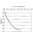
- the intermediate contact layer 93 has a thickness of 70 nm and the top layer 91 has a thickness of 250 nm
- a range of about 100 to 300 nm is preferable as a range that does not penetrate the top layer 91 through the intermediate contact layer 93.
- the machining depth in this range is approximated with high accuracy by the above equation (1).
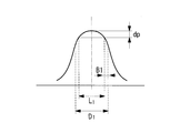
- the intermediate contact layer separation grooves 14 are formed in a series by partially overlapping separation holes 14a having a diameter D1 of about the laser beam spot diameter (for example, 124 ⁇ m). Yes.
- the left-right direction is the extending direction of the intermediate separation groove 14.
- the overlapping width B1 of the adjacent separation holes 14a is set to 0% or more and 5% or less of the diameter D1 of the separation holes 14a. Since the width that can be processed by one laser irradiation is proportional to L1 (D1-2 * B1), the processing speed increases as the overlap width B1 decreases.
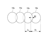
- the overlap width B2 is equal to the separation hole 14a. It was 10 to 20% of the diameter.
- FIG. 4B showing the case of the picosecond pulse laser according to the present embodiment will be described in comparison with FIG. 5B showing the case of the nanosecond pulse laser.
- the horizontal axis indicates the position centered on the optical axis of the laser
- the vertical axis indicates the energy density used for grooving.
- 4B and 5B both have the energy density of the Gaussian distribution shape centered on the laser optical axis in the pulse laser, and therefore the energy density used for the groove processing after being introduced from the laser is also the Gaussian distribution shape. Become. However, as shown in FIG.
- the pulse width of the pulse laser used when separating the intermediate contact layer 93 is set to 10 ps or more and 750 ps or less, which is significantly shorter than the conventional pulse width set to nanoseconds, and the time of heat energy given to the top layer 91 The interval was extremely short.
- the amorphous silicon of the top layer 91 is melted and scattered at an extremely short time interval as compared with a laser having a pulse width of nanoseconds, so that excessive heat is applied to the wall portion forming the intermediate contact layer separation groove 14. It will not be taken away. Therefore, the region where silicon is recrystallized at the wall portion forming the intermediate contact layer isolation groove 14 can be made as small as possible.
- the region where the resistance of silicon is recrystallized and reduced in resistance can be reduced, the current leaking through the intermediate contact layer isolation trench can be reduced.
- the intermediate contact layer separation groove 14 is terminated at a midway position of the top layer 91 and is not allowed to reach the transparent electrode layer 2 connected to the top layer 91. As a result, even if a recrystallized region is formed in the wall portion forming the intermediate contact layer separation groove 14, the recrystallized region is not physically connected to the transparent electrode layer 2. The layer 93 and the transparent electrode layer 2 are not electrically connected.
- the pulse laser Since the pulse laser has a pulse width of 10 ps or more and 750 ps or less, heat energy can be given to the top layer 91 at an extremely short time interval.
- the thermal diffusion in which the input thermal energy is absorbed and diffused by the amorphous silicon of the top layer 91 can be suppressed, so that the separation hole 14a ( Sufficient thermal energy can be input to the vicinity of the periphery of FIG. 4A), and the separation hole 14a formed to a desired depth can be formed to the vicinity of the periphery of the separation hole 14a. Therefore, the overlapping width of the adjacent separation holes 14a can be reduced to 0% or more and 5% or less of the diameter of the separation holes, and as a result, the processing speed can be increased.
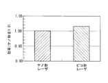
- FIG. 6 shows the efficiency of the solar cell module manufactured by the manufacturing method according to this embodiment using a picosecond pulse laser with a pulse width of 13 ps, and, as a comparative example, a nanometer instead of a picosecond pulse laser with a pulse width of 15 ns. It shows the efficiency of a solar cell module manufactured using a second pulse laser.
- a comparative example using a nanosecond pulse laser is normalized to 1.0 for a solar cell module with an output of 130 to 135 W
- this embodiment using a picosecond pulse laser is used. Then, the efficiency improved by 1.02 times (2% improvement).
- the solar cell shown in FIG. 1 has a tandem structure in which two power generation layers including the first cell layer 91 and the second cell layer 92 are stacked.
- the present invention is limited to the tandem structure. This is widely applicable when the silicon-based material is recrystallized when laser processing the intermediate contact layer separation groove. For example, three power generation layers are stacked, and the intermediate contact layer is formed between the power generation layers. It can also be used for a triple structure provided with.
Landscapes
- Photovoltaic Devices (AREA)
- Chemical & Material Sciences (AREA)
- Crystallography & Structural Chemistry (AREA)
Abstract
Priority Applications (3)
| Application Number | Priority Date | Filing Date | Title |
|---|---|---|---|
| CN2009801290371A CN102105993B (zh) | 2008-11-05 | 2009-10-02 | 光电转换装置的制造方法及光电转换装置 |
| US13/054,858 US8835253B2 (en) | 2008-11-05 | 2009-10-02 | Photoelectric conversion device fabrication method and photoelectric conversion device |
| EP09824682A EP2346088A1 (fr) | 2008-11-05 | 2009-10-02 | Procede de production de dispositif de conversion photoelectrique et dispositif de conversion photoelectrique |
Applications Claiming Priority (2)
| Application Number | Priority Date | Filing Date | Title |
|---|---|---|---|
| JP2008-284208 | 2008-11-05 | ||
| JP2008284208A JP2010114190A (ja) | 2008-11-05 | 2008-11-05 | 光電変換装置の製造方法および光電変換装置 |
Publications (1)
| Publication Number | Publication Date |
|---|---|
| WO2010052982A1 true WO2010052982A1 (fr) | 2010-05-14 |
Family
ID=42152792
Family Applications (1)
| Application Number | Title | Priority Date | Filing Date |
|---|---|---|---|
| PCT/JP2009/067250 Ceased WO2010052982A1 (fr) | 2008-11-05 | 2009-10-02 | Procédé de production de dispositif de conversion photoélectrique et dispositif de conversion photoélectrique |
Country Status (6)
| Country | Link |
|---|---|
| US (1) | US8835253B2 (fr) |
| EP (1) | EP2346088A1 (fr) |
| JP (1) | JP2010114190A (fr) |
| KR (1) | KR20110031335A (fr) |
| CN (1) | CN102105993B (fr) |
| WO (1) | WO2010052982A1 (fr) |
Cited By (1)
| Publication number | Priority date | Publication date | Assignee | Title |
|---|---|---|---|---|
| DE102011017807A1 (de) * | 2011-04-29 | 2012-10-31 | Trumpf Laser- Und Systemtechnik Gmbh | Verfahren zum laserinduzierten Entfernen von Bereichen von Schichten eines Schichtenstapels |
Families Citing this family (7)
| Publication number | Priority date | Publication date | Assignee | Title |
|---|---|---|---|---|
| JP2010251428A (ja) * | 2009-04-13 | 2010-11-04 | Mitsubishi Heavy Ind Ltd | 光電変換装置の製造方法、光電変換装置の製造装置、及び光電変換装置 |
| WO2011114761A1 (fr) * | 2010-03-18 | 2011-09-22 | 富士電機システムズ株式会社 | Cellule solaire à couches minces et son procédé de fabrication |
| US20130167916A1 (en) * | 2011-12-28 | 2013-07-04 | Taiwan Semiconductor Manufacturing Co., Ltd. | Thin film photovoltaic cells and methods of forming the same |
| DE102012205378A1 (de) * | 2012-04-02 | 2013-10-02 | Robert Bosch Gmbh | Verfahren zur Herstellung von Dünnschichtsolarmodulen sowie nach diesem Verfahren erhältliche Dünnschichtsolarmodule |
| CN103746027B (zh) * | 2013-12-11 | 2015-12-09 | 西安交通大学 | 一种在ito导电薄膜表面刻蚀极细电隔离槽的方法 |
| US9330955B2 (en) | 2013-12-31 | 2016-05-03 | Applied Materials, Inc. | Support ring with masked edge |
| EP4415057A1 (fr) * | 2023-02-13 | 2024-08-14 | Nivarox-FAR S.A. | Cellule solaire transparente pour appareil electronique et procede de fabrication de ladite cellule solaire |
Citations (9)
| Publication number | Priority date | Publication date | Assignee | Title |
|---|---|---|---|---|
| JPS616828A (ja) * | 1984-06-20 | 1986-01-13 | Sanyo Electric Co Ltd | 集積型光起電力装置の製造方法 |
| JPS6240986A (ja) * | 1985-08-20 | 1987-02-21 | Fuji Electric Corp Res & Dev Ltd | レ−ザ−加工方法 |
| JPH05218472A (ja) * | 1991-10-07 | 1993-08-27 | Siemens Ag | 薄膜構成体のレーザ加工方法 |
| JPH08330617A (ja) * | 1995-05-30 | 1996-12-13 | Sanyo Electric Co Ltd | 光起電力モジュールの製造方法 |
| JP2001274447A (ja) * | 2000-03-23 | 2001-10-05 | Kanegafuchi Chem Ind Co Ltd | 集積型薄膜太陽電池の製造方法 |
| JP2002261308A (ja) | 2001-03-01 | 2002-09-13 | Kanegafuchi Chem Ind Co Ltd | 薄膜光電変換モジュール |
| JP2005101412A (ja) * | 2003-09-26 | 2005-04-14 | Sanyo Electric Co Ltd | 光起電力装置の製造方法 |
| JP2005101413A (ja) * | 2003-09-26 | 2005-04-14 | Disco Abrasive Syst Ltd | 薄板状被加工物の分割方法及び装置 |
| JP2006313872A (ja) | 2005-04-06 | 2006-11-16 | Mitsubishi Heavy Ind Ltd | 多接合薄膜太陽電池 |
Family Cites Families (26)
| Publication number | Priority date | Publication date | Assignee | Title |
|---|---|---|---|---|
| US4713518A (en) * | 1984-06-08 | 1987-12-15 | Semiconductor Energy Laboratory Co., Ltd. | Electronic device manufacturing methods |
| US4650524A (en) * | 1984-06-20 | 1987-03-17 | Sanyo Electric Co., Ltd | Method for dividing semiconductor film formed on a substrate into plural regions by backside energy beam irradiation |
| JPS63121813A (ja) | 1986-11-11 | 1988-05-25 | Minolta Camera Co Ltd | レ−ザ−切断用光学系 |
| US5072091A (en) * | 1989-04-03 | 1991-12-10 | The Local Government Of Osaka Prefecture | Method and apparatus for metal surface process by laser beam |
| JPH0582816A (ja) | 1991-09-24 | 1993-04-02 | Sanyo Electric Co Ltd | 光起電力装置とその製造方法 |
| JPH0727994A (ja) | 1993-07-12 | 1995-01-31 | Toshiba Corp | ビーム分布均一化装置 |
| JPH07308788A (ja) * | 1994-05-16 | 1995-11-28 | Sanyo Electric Co Ltd | 光加工法及び光起電力装置の製造方法 |
| US5880430A (en) * | 1995-08-11 | 1999-03-09 | Wein; Joseph H. | Method and apparatus for laser engraving |
| US5864430A (en) * | 1996-09-10 | 1999-01-26 | Sandia Corporation | Gaussian beam profile shaping apparatus, method therefor and evaluation thereof |
| JPH10258385A (ja) | 1997-03-14 | 1998-09-29 | Komatsu Ltd | レーザ加工機、レーザ加工機の加工方法、及びレーザ加工機用マスク |
| US6632993B2 (en) * | 2000-10-05 | 2003-10-14 | Kaneka Corporation | Photovoltaic module |
| JP2003273383A (ja) * | 2002-03-15 | 2003-09-26 | Sharp Corp | 太陽電池素子およびその製造方法 |
| JP2003298089A (ja) | 2002-04-02 | 2003-10-17 | Kanegafuchi Chem Ind Co Ltd | タンデム型薄膜光電変換装置とその製造方法 |
| US20050155956A1 (en) * | 2002-08-30 | 2005-07-21 | Sumitomo Heavy Industries, Ltd. | Laser processing method and processing device |
| GB2402230B (en) * | 2003-05-30 | 2006-05-03 | Xsil Technology Ltd | Focusing an optical beam to two foci |
| JP4365636B2 (ja) | 2003-07-15 | 2009-11-18 | 京セラ株式会社 | 集積型光電変換装置 |
| EP1732139B1 (fr) * | 2004-03-25 | 2018-12-12 | Kaneka Corporation | Procédé de fabrication d'un substrat pour cellule solaire à film mince |
| JP2006080205A (ja) | 2004-09-08 | 2006-03-23 | Sumitomo Heavy Ind Ltd | レーザ加工装置及びレーザ加工方法 |
| JP2006110587A (ja) | 2004-10-14 | 2006-04-27 | Canon Inc | レーザー干渉加工方法および装置 |
| JP2005099858A (ja) | 2004-12-06 | 2005-04-14 | Dainippon Printing Co Ltd | 回折格子を用いた絵柄体の製造方法 |
| US7235736B1 (en) * | 2006-03-18 | 2007-06-26 | Solyndra, Inc. | Monolithic integration of cylindrical solar cells |
| US8624157B2 (en) * | 2006-05-25 | 2014-01-07 | Electro Scientific Industries, Inc. | Ultrashort laser pulse wafer scribing |
| US7982127B2 (en) * | 2006-12-29 | 2011-07-19 | Industrial Technology Research Institute | Thin film solar cell module of see-through type |
| EP2187449A1 (fr) * | 2007-08-14 | 2010-05-19 | Mitsubishi Heavy Industries, Ltd. | Dispositif de conversion photoélectrique et son procédé de fabrication |
| TWI378565B (en) * | 2008-04-30 | 2012-12-01 | Nexpower Technology Corp | Stacked-layered thin film solar cell and manufacturing method thereof |
| US7999175B2 (en) * | 2008-09-09 | 2011-08-16 | Palo Alto Research Center Incorporated | Interdigitated back contact silicon solar cells with laser ablated grooves |
-
2008
- 2008-11-05 JP JP2008284208A patent/JP2010114190A/ja active Pending
-
2009
- 2009-10-02 EP EP09824682A patent/EP2346088A1/fr not_active Withdrawn
- 2009-10-02 US US13/054,858 patent/US8835253B2/en not_active Expired - Fee Related
- 2009-10-02 KR KR1020117001267A patent/KR20110031335A/ko not_active Ceased
- 2009-10-02 CN CN2009801290371A patent/CN102105993B/zh not_active Expired - Fee Related
- 2009-10-02 WO PCT/JP2009/067250 patent/WO2010052982A1/fr not_active Ceased
Patent Citations (9)
| Publication number | Priority date | Publication date | Assignee | Title |
|---|---|---|---|---|
| JPS616828A (ja) * | 1984-06-20 | 1986-01-13 | Sanyo Electric Co Ltd | 集積型光起電力装置の製造方法 |
| JPS6240986A (ja) * | 1985-08-20 | 1987-02-21 | Fuji Electric Corp Res & Dev Ltd | レ−ザ−加工方法 |
| JPH05218472A (ja) * | 1991-10-07 | 1993-08-27 | Siemens Ag | 薄膜構成体のレーザ加工方法 |
| JPH08330617A (ja) * | 1995-05-30 | 1996-12-13 | Sanyo Electric Co Ltd | 光起電力モジュールの製造方法 |
| JP2001274447A (ja) * | 2000-03-23 | 2001-10-05 | Kanegafuchi Chem Ind Co Ltd | 集積型薄膜太陽電池の製造方法 |
| JP2002261308A (ja) | 2001-03-01 | 2002-09-13 | Kanegafuchi Chem Ind Co Ltd | 薄膜光電変換モジュール |
| JP2005101412A (ja) * | 2003-09-26 | 2005-04-14 | Sanyo Electric Co Ltd | 光起電力装置の製造方法 |
| JP2005101413A (ja) * | 2003-09-26 | 2005-04-14 | Disco Abrasive Syst Ltd | 薄板状被加工物の分割方法及び装置 |
| JP2006313872A (ja) | 2005-04-06 | 2006-11-16 | Mitsubishi Heavy Ind Ltd | 多接合薄膜太陽電池 |
Cited By (1)
| Publication number | Priority date | Publication date | Assignee | Title |
|---|---|---|---|---|
| DE102011017807A1 (de) * | 2011-04-29 | 2012-10-31 | Trumpf Laser- Und Systemtechnik Gmbh | Verfahren zum laserinduzierten Entfernen von Bereichen von Schichten eines Schichtenstapels |
Also Published As
| Publication number | Publication date |
|---|---|
| JP2010114190A (ja) | 2010-05-20 |
| EP2346088A1 (fr) | 2011-07-20 |
| CN102105993B (zh) | 2013-03-27 |
| US20110126894A1 (en) | 2011-06-02 |
| US8835253B2 (en) | 2014-09-16 |
| CN102105993A (zh) | 2011-06-22 |
| KR20110031335A (ko) | 2011-03-25 |
Similar Documents
| Publication | Publication Date | Title |
|---|---|---|
| JP5459901B2 (ja) | 光電変換装置モジュールの作製方法 | |
| WO2010119581A1 (fr) | Procédé de fabrication de dispositif de conversion photoélectrique, dispositif de fabrication de dispositif de conversion photoélectrique et dispositif de conversion photoélectrique | |
| JP5180781B2 (ja) | 光電変換装置の製造方法および光電変換装置 | |
| CN102105993B (zh) | 光电转换装置的制造方法及光电转换装置 | |
| JP2011056514A (ja) | 光電変換素子の製造方法 | |
| JP4648105B2 (ja) | 太陽電池モジュール及び太陽電池モジュールの製造方法 | |
| JP5022341B2 (ja) | 光電変換装置 | |
| JP7349509B2 (ja) | 太陽電池の製造方法 | |
| JPH1079522A (ja) | 薄膜光電変換装置およびその製造方法 | |
| JP2012038902A (ja) | 集積型光電変換装置の製造方法 | |
| JP4786010B2 (ja) | 集積型ハイブリッド薄膜太陽電池の製造方法 | |
| JP2011061017A (ja) | 光電変換装置の製造方法 | |
| JP2009094272A (ja) | 光電変換モジュールおよび光電変換モジュールの製造方法 | |
| JP2011155026A (ja) | 光電変換装置の製造方法 | |
| JP4875566B2 (ja) | 光電変換装置の製造方法 | |
| JP2006019715A (ja) | 太陽電池及び太陽電池の製造方法 | |
| JP2013140850A (ja) | 光電変換装置及びその製造方法 | |
| WO2009081855A1 (fr) | Procédé de fabrication de dispositif de conversion photoélectrique et dispositif de conversion photoélectrique | |
| WO2011033885A1 (fr) | Dispositif de conversion photoélectrique | |
| JP2010251424A (ja) | 光電変換装置 | |
| JP2010199305A (ja) | 光電変換装置の製造方法 | |
| JP2011077380A (ja) | 光電変換装置 |
Legal Events
| Date | Code | Title | Description |
|---|---|---|---|
| WWE | Wipo information: entry into national phase |
Ref document number: 200980129037.1 Country of ref document: CN |
|
| 121 | Ep: the epo has been informed by wipo that ep was designated in this application |
Ref document number: 09824682 Country of ref document: EP Kind code of ref document: A1 |
|
| ENP | Entry into the national phase |
Ref document number: 20117001267 Country of ref document: KR Kind code of ref document: A |
|
| WWE | Wipo information: entry into national phase |
Ref document number: 13054858 Country of ref document: US |
|
| WWE | Wipo information: entry into national phase |
Ref document number: 2009824682 Country of ref document: EP |
|
| NENP | Non-entry into the national phase |
Ref country code: DE |