WO2010092908A1 - Sonde à ultrasons et dispositif de diagnostic ultrasonore - Google Patents
Sonde à ultrasons et dispositif de diagnostic ultrasonore Download PDFInfo
- Publication number
- WO2010092908A1 WO2010092908A1 PCT/JP2010/051688 JP2010051688W WO2010092908A1 WO 2010092908 A1 WO2010092908 A1 WO 2010092908A1 JP 2010051688 W JP2010051688 W JP 2010051688W WO 2010092908 A1 WO2010092908 A1 WO 2010092908A1
- Authority
- WO
- WIPO (PCT)
- Prior art keywords
- electrode
- layer
- ultrasonic
- element layer
- ultrasonic probe
- Prior art date
- Legal status (The legal status is an assumption and is not a legal conclusion. Google has not performed a legal analysis and makes no representation as to the accuracy of the status listed.)
- Ceased
Links
Images


Classifications
-
- B—PERFORMING OPERATIONS; TRANSPORTING
- B06—GENERATING OR TRANSMITTING MECHANICAL VIBRATIONS IN GENERAL
- B06B—METHODS OR APPARATUS FOR GENERATING OR TRANSMITTING MECHANICAL VIBRATIONS OF INFRASONIC, SONIC, OR ULTRASONIC FREQUENCY, e.g. FOR PERFORMING MECHANICAL WORK IN GENERAL
- B06B1/00—Methods or apparatus for generating mechanical vibrations of infrasonic, sonic, or ultrasonic frequency
- B06B1/02—Methods or apparatus for generating mechanical vibrations of infrasonic, sonic, or ultrasonic frequency making use of electrical energy
- B06B1/06—Methods or apparatus for generating mechanical vibrations of infrasonic, sonic, or ultrasonic frequency making use of electrical energy operating with piezoelectric effect or with electrostriction
- B06B1/0607—Methods or apparatus for generating mechanical vibrations of infrasonic, sonic, or ultrasonic frequency making use of electrical energy operating with piezoelectric effect or with electrostriction using multiple elements
- B06B1/0622—Methods or apparatus for generating mechanical vibrations of infrasonic, sonic, or ultrasonic frequency making use of electrical energy operating with piezoelectric effect or with electrostriction using multiple elements on one surface
-
- A—HUMAN NECESSITIES
- A61—MEDICAL OR VETERINARY SCIENCE; HYGIENE
- A61B—DIAGNOSIS; SURGERY; IDENTIFICATION
- A61B8/00—Diagnosis using ultrasonic, sonic or infrasonic waves
- A61B8/44—Constructional features of the ultrasonic, sonic or infrasonic diagnostic device
- A61B8/4483—Constructional features of the ultrasonic, sonic or infrasonic diagnostic device characterised by features of the ultrasound transducer
-
- B—PERFORMING OPERATIONS; TRANSPORTING
- B06—GENERATING OR TRANSMITTING MECHANICAL VIBRATIONS IN GENERAL
- B06B—METHODS OR APPARATUS FOR GENERATING OR TRANSMITTING MECHANICAL VIBRATIONS OF INFRASONIC, SONIC, OR ULTRASONIC FREQUENCY, e.g. FOR PERFORMING MECHANICAL WORK IN GENERAL
- B06B1/00—Methods or apparatus for generating mechanical vibrations of infrasonic, sonic, or ultrasonic frequency
- B06B1/02—Methods or apparatus for generating mechanical vibrations of infrasonic, sonic, or ultrasonic frequency making use of electrical energy
- B06B1/06—Methods or apparatus for generating mechanical vibrations of infrasonic, sonic, or ultrasonic frequency making use of electrical energy operating with piezoelectric effect or with electrostriction
- B06B1/0607—Methods or apparatus for generating mechanical vibrations of infrasonic, sonic, or ultrasonic frequency making use of electrical energy operating with piezoelectric effect or with electrostriction using multiple elements
- B06B1/0622—Methods or apparatus for generating mechanical vibrations of infrasonic, sonic, or ultrasonic frequency making use of electrical energy operating with piezoelectric effect or with electrostriction using multiple elements on one surface
- B06B1/064—Methods or apparatus for generating mechanical vibrations of infrasonic, sonic, or ultrasonic frequency making use of electrical energy operating with piezoelectric effect or with electrostriction using multiple elements on one surface with multiple active layers
-
- A—HUMAN NECESSITIES
- A61—MEDICAL OR VETERINARY SCIENCE; HYGIENE
- A61B—DIAGNOSIS; SURGERY; IDENTIFICATION
- A61B8/00—Diagnosis using ultrasonic, sonic or infrasonic waves
- A61B8/13—Tomography
Definitions
- the present invention relates to an ultrasonic probe and an ultrasonic diagnostic apparatus.
- the ultrasonic diagnostic apparatus is a medical imaging device that obtains a tomographic image of a soft tissue in a living body from a body surface in a minimally invasive manner by an ultrasonic pulse reflection method.
- this ultrasound diagnostic device has features such as being smaller and cheaper, without exposure to X-rays, etc., being highly safe, and capable of blood flow imaging by applying the Doppler effect. Yes. Therefore, it is widely used in the circulatory system (cardiac coronary artery), digestive system (gastrointestinal), internal medicine system (liver, pancreas, spleen), urology system (kidney, bladder), and obstetrics and gynecology.
- an inorganic piezoelectric element called PZT is generally used in order to transmit and receive high-sensitivity and high-resolution ultrasonic waves.
- a vibration mode of the transmitting piezoelectric element a single-type probe or an array-type probe in which a plurality of probes are two-dimensionally arranged is often used. Since the array type can obtain a fine image, it is widely used as a medical image for a diagnostic examination.
- harmonic imaging diagnosis using harmonic signals is becoming a standard diagnosis method because a clear diagnosis image that cannot be obtained by conventional B-mode diagnosis is obtained.
- Harmonic imaging has many advantages compared to the fundamental wave as follows.
- the S / N ratio is good and the contrast resolution is good because the side lobe level is small.
- Attenuation beyond the focal point is similar to that of the fundamental wave, and the deep velocity can be increased compared to ultrasonic waves with the harmonic frequency as the fundamental wave.
- the receiving piezoelectric vibrator used in such an array type ultrasonic probe can receive a harmonic signal with high sensitivity.
- the transmission / reception frequency of the inorganic piezoelectric element depends on the thickness of the inorganic piezoelectric element, it is necessary to process the inorganic piezoelectric element in a smaller size as the receiving frequency becomes higher, and the manufacturing is difficult.
- the present inventors made a single layer or a laminate of a transmission piezoelectric element having a structure in which a sheet-like piezoelectric ceramic is single-layered or laminated and a sheet-shaped piezoelectric element for reception to transmit and transmit.
- a method of obtaining a high-sensitivity ultrasonic probe by separating reception into separate piezoelectric elements and using a high-sensitivity organic piezoelectric element material for reception has been proposed (see Patent Documents 1, 2, and 3). ).
- connection method between the electrode of the piezoelectric element used in the ultrasonic probe and the wiring member is important.
- the signal quality transmitted / received from the ultrasonic probe may deteriorate, or the connection reliability may be poor. It also affects the performance and reliability of ultrasonic diagnostic equipment.
- JP 2008-188415 A International Publication No. 2007/145073 International Publication No. 2008/010509 Japanese Patent No. 3313171 Japanese Patent Laid-Open No. 7-194517 Japanese Patent No. 3280677 Japanese Patent Laid-Open No. 11-276479 Japanese Patent No. 3304560
- the array type ultrasonic probe used for harmonic imaging has a low yield because the space for connecting to the lead wire is limited and cannot be used.
- the present invention has been made in view of the above problems, and provides an ultrasonic probe that can reliably connect an electrode of a piezoelectric element and a wiring member, and a highly reliable ultrasonic probe.
- An object of the present invention is to provide an ultrasonic diagnostic apparatus.
- the present invention has the following characteristics.
- At least one transmission element layer that transmits ultrasonic waves at least one reception element layer that receives ultrasonic waves each having electrodes formed on both surfaces facing each other in the thickness direction, and at least one layer matching acoustic impedance
- a circuit board having a conductive portion formed on a surface facing the thickness direction of the substrate material;
- the circuit board is The electrode formed on the surface of the upper protruding portion or the surface of the upper protruding portion, the end surface of the receiving element layer, the surface of the lower protruding portion or the surface of the lower protruding portion
- the conductive portion formed on the surface of the substrate material is inserted into at least one of the electrodes formed on the upper layer or the lower layer in the at least part of a recess surrounded by the electrode.
- the tip of the circuit board inserted into the recess is 3.
- the length in the elevation direction of the protrusion of the upper layer is 2% or more of the length in the elevation direction of the upper layer, and the length in the elevation direction of the protrusion of the lower layer is the elevation of the lower layer. 2% or more of the length in the direction of The length of the receiving element layer is: 4.
- the thickness of the portion including the conductive portion inserted into the concave portion of the circuit board is: 5.
- An ultrasonic diagnostic apparatus comprising the ultrasonic probe according to any one of 1 to 5 above.
- the upper layer and the lower layer sandwiching the electrodes formed on both sides of the receiving element layer, respectively are provided with protrusions protruding from the receiving element layer in the elevation direction, and at least of the electrodes formed on both sides One is formed to extend to the upper layer or lower layer protrusion, and is joined to the opposing surface of the upper layer or lower layer.
- FIG. 1 is a diagram illustrating an external configuration of an ultrasonic diagnostic apparatus 100 according to an embodiment.
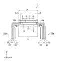
- 1 is a block diagram showing an electrical configuration of an ultrasonic diagnostic apparatus 100 in an embodiment. It is sectional drawing which shows the structure of the head part of the ultrasonic probe of 1st Embodiment. It is sectional drawing which shows the connection of the recessed part 17 and circuit board 25 of 1st Embodiment.
- FIG. 4 is an enlarged cross-sectional view of a portion of a circuit board 25 inserted into a recess 17. It is sectional drawing which shows the connection of the receiving element layer 3 of 2nd Embodiment, and a flexible substrate.
- FIG. 1 is a diagram illustrating an external configuration of an ultrasonic diagnostic apparatus according to an embodiment.
- FIG. 2 is a block diagram illustrating an electrical configuration of the ultrasonic diagnostic apparatus according to the embodiment.
- the ultrasonic diagnostic apparatus 100 transmits an ultrasonic wave (ultrasonic signal) to a subject such as a living body (not shown), and receives the ultrasonic wave reflected from the received subject (echo, ultrasonic signal).
- the internal state in the sample is imaged as an ultrasonic image and displayed on the display unit 45.
- the ultrasonic probe 1 transmits an ultrasonic wave (ultrasonic signal) to the subject and receives a reflected wave of the ultrasonic wave reflected by the subject. As shown in FIG. 2, the ultrasonic probe 1 is connected to the ultrasonic diagnostic apparatus main body 31 via a cable 33, and is electrically connected to the transmission circuit 42 and the reception circuit 43.
- the transmission circuit 42 transmits an electrical signal to the ultrasonic probe 1 via the cable 33 in accordance with a command from the control unit 46, and transmits ultrasonic waves from the ultrasonic probe 1 to the subject.
- the receiving circuit 43 receives an electrical signal corresponding to the reflected wave of the ultrasonic wave from the inside of the subject via the cable 33 from the ultrasonic probe 1 in accordance with an instruction from the control unit 46.
- the image processing unit 44 images the internal state in the subject as an ultrasonic image based on the electrical signal received by the receiving circuit 43 in accordance with an instruction from the control unit 46.
- the display unit 45 is composed of a liquid crystal panel or the like, and displays an ultrasonic image imaged by the image processing unit 44 according to a command from the control unit 46.
- the operation input unit 41 includes a switch, a keyboard, and the like, and is provided for the user to input data such as a command for instructing the start of diagnosis and personal information of the subject.
- the control unit 46 includes a CPU, a memory, and the like, and controls each part of the ultrasonic diagnostic apparatus 100 according to a programmed procedure based on an input from the operation input unit 41.
- FIG. 3 is a cross-sectional view showing the configuration of the head portion of the ultrasonic probe according to the first embodiment.
- the X direction is the elevation direction (the dicing direction), and the Z-axis positive direction is the direction in which ultrasonic waves are transmitted.
- the Z-axis direction is the stacking direction.
- the ultrasonic probe 1 shown in FIG. 3 includes a fourth electrode 15, a transmission element layer 2, a third electrode 14, an intermediate layer 13, a second electrode 10, a reception element layer 3, and a first electrode on a backing material 5. 9, the matching layer 6 and the acoustic lens 7 are laminated in this order.
- the transmitting element layer 2 is a piezoelectric element made of an inorganic piezoelectric material such as PZT (lead zirconate titanate), and includes a third electrode 14 and a fourth electrode 15 on both surfaces facing each other in the thickness direction.
- the thickness of the transmitting element layer 2 is about 320 ⁇ m.
- the third electrode 14 and the fourth electrode 15 are connected to the cable 33 by a connector (not shown), and are connected to the transmission circuit 42 via the cable 33.
- the piezoelectric element vibrates and transmits ultrasonic waves from the transmitting element layer 2 in the positive Z-axis direction.
- the thickness of the third electrode 14 and the fourth electrode 15 is about 1 to 2 ⁇ m.
- the thicknesses of the third electrode 14 and the fourth electrode 15 are preferably as thin as possible in terms of acoustic characteristics. However, if the thickness is too thin, cracking or the like occurs in the electrode and the reliability is impaired, so the range of 0.1 to 10 ⁇ m is preferable. It is desirable that the thickness is 0.1 to 5 ⁇ m. In particular, it is desirable that the fourth electrode 15 on the ultrasonic wave transmitting side be as thin as possible in terms of acoustic characteristics.
- the third electrode 14 and the fourth electrode 15 are formed by vapor deposition or photolithography on both surfaces of the transmission element layer 2 using a metal material such as gold, silver, or aluminum.
- the intermediate layer 13 is made of a resin material.
- the intermediate layer 13 couples the second electrode 10 and the third electrode 14, and when the receiving element layer 3 receives and vibrates the reflected ultrasonic wave reflected by the subject, the transmitting element layer 2 resonates. Therefore, it is provided to absorb the vibration of the receiving element layer 3 so as not to vibrate.
- the resin material used for the intermediate layer 13 for example, polyvinyl butyral, polyolefin, polyacrylate, polyimide, polyamide, polyester, polysulfone, epoxy, oxetane, and the like can be used. Furthermore, fine particles for adjusting the characteristics may be added to these resins.
- the thickness of the intermediate layer 13 is selected depending on the required sensitivity and frequency characteristics, and is, for example, about 180 to 190 ⁇ m. Further, the intermediate layer 13 can be omitted depending on the required sensitivity and frequency characteristics.
- the receiving element layer 3 is composed of a plurality of piezoelectric elements made of an organic piezoelectric material.
- a vinylidene fluoride polymer can be used as the organic piezoelectric material used for the receiving element layer 3.
- a vinylidene fluoride (VDF) copolymer can be used as the organic piezoelectric material.
- This vinylidene fluoride copolymer is a copolymer (copolymer) of vinylidene fluoride and other monomers. Examples of other monomers include ethylene trifluoride (TrFE) and tetrafluoroethylene (TeFE).
- Perfluoroalkyl vinyl ether (PFA), perfluoroalkoxyethylene (PAE), perfluorohexaethylene, and the like can be used.
- a piezoelectric element made of an inorganic piezoelectric material can receive only an ultrasonic wave having a frequency band of about twice the frequency of the fundamental wave, whereas a piezoelectric element made of an organic piezoelectric material is, for example, 4 to 5 times the frequency of the fundamental wave.
- Ultrasonic waves in a certain frequency band can be received, which is suitable for widening the reception frequency band. Since the ultrasonic signal is received by the organic piezoelectric element 21 having a characteristic capable of receiving such ultrasonic waves over a wide frequency range, the ultrasonic probe 1 and the ultrasonic diagnostic apparatus 100 in the present embodiment are compared.
- the frequency band can be widened with a simple structure.
- the thickness of the receiving element layer 3 is appropriately set depending on the frequency of the ultrasonic wave to be received, the type of the organic piezoelectric material, and the like. For example, when receiving an ultrasonic wave having a center frequency of 15 MHz, the thickness of the receiving element layer 3 The thickness is about 35 to 40 ⁇ m.
- Such a receiving element layer 3 is cast from a solution of an organic piezoelectric material to form a film having a predetermined thickness, heated for crystallization, and then formed into a sheet having a predetermined size. Make it.
- the first electrode 9 and the second electrode 10 are formed on both surfaces of the receiving element layer 3 facing each other in the thickness direction (Z-axis direction).
- the thicknesses of the first electrode 9 and the second electrode 10 are about 1 to 2 ⁇ m.
- the electrode of the receiving element layer 3 should be as thin as possible in terms of acoustic characteristics. However, if the electrode is too thin, cracks or the like occur in the electrode and impair reliability, so the range is 0.1 to 10 ⁇ m, preferably 0.1 to 5 ⁇ m. It is desirable to do. Since the receiving element layer 3 receives high-frequency harmonics, it is desirable that both the first electrode 9 and the second electrode 10 be as thin as possible in terms of acoustic characteristics.
- the first electrode 9 and the second electrode 10 are formed by vapor deposition or photolithography using a metal material such as gold, silver, or aluminum.
- the electrode used for the receiving element layer 3, particularly the first electrode 9, needs to be formed very thin in order to receive harmonics with high sensitivity. Therefore, it is desirable to use gold having good conductivity as the metal material.
- the first electrode 9 and the second electrode 10 are connected to the receiving circuit 43 via the cable 33.
- the receiving element layer 3 When the receiving element layer 3 receives and vibrates the reflected wave of the ultrasonic wave reflected by the subject, an electrical signal is generated between the first electrode 9 and the second electrode 10 in the piezoelectric element according to the reflected wave.
- the electrical signal generated between the first electrode 9 and the second electrode 10 is received by the receiving circuit 43 via the cable 33 and imaged by the image processing unit 44.
- the matching layer 6 has an acoustic impedance intermediate between the acoustic impedances of the respective layers, and aims to match the acoustic impedance.
- the matching layer 6 is a single layer is illustrated, but a multi-layer case may be used.
- the thickness of the matching layer 6 is, for example, about 140 ⁇ m.
- the acoustic lens 7 is made of silicone or resin, and converges transmitted or received ultrasonic waves to a predetermined distance.
- the layers 6 are laminated in the order as shown in FIG. After lamination, dicing is performed in the X-axis direction from the matching layer 18 in the direction opposite to the ultrasonic radiation direction, and further dicing is performed from the backing material and the adhesive layer of the fourth electrode in the negative Z-axis direction. After filling the groove portion formed by dicing with a filler made of silicone resin or the like, the acoustic lens 7 is bonded to the uppermost layer.
- the upper layer sandwiching the first electrode 9 and the second electrode 10 formed in the receiving element layer 3 is the matching layer 6, and the lower layer is the intermediate layer 13.
- the matching layer 6 and the intermediate layer 13 include protrusions 18 a and 18 b and protrusions 19 a and 19 b that protrude from the receiving element layer 3.
- first electrode 9 is formed to extend to the surface facing the intermediate layer 13 of the projecting portions 18a and 18b
- second electrode 10 is extended to the surface facing the matching layer 6 of the projecting portions 19a and 19b. Is formed.
- a metal thin film serving as an electrode is formed in advance on at least the protruding portions 18a and 18b on the surface of the matching layer 6 facing the first electrode 9 by using a metal material such as gold, silver, or aluminum by vapor deposition or photolithography. Film.
- the first electrode 9 formed on the receiving element layer 3 and the metal thin film formed on the matching layer 6 are joined with a conductive adhesive or the like, and the first electrode 9 is connected to the protruding portion 18a, Extend to 18b.
- the second electrode 10 can be formed to extend to the surface of the protrusions 19a and 19b facing the matching layer 6 by a similar method.
- a metal thin film serving as an electrode is formed in advance on at least the protruding portions 19a and 19b on the surface of the intermediate layer 13 facing the second electrode 10 by using a metal material such as gold, silver, or aluminum by vapor deposition or photolithography. Film.
- a metal material such as gold, silver, or aluminum by vapor deposition or photolithography. Film.
- the second electrode 10 formed on the receiving element layer 3 and the metal thin film formed on the matching layer 6 are joined with a conductive adhesive or the like, and the second electrode 10 is connected to the protruding portion 19a, Extend to 19b.
- the protruding portions 18a and 18b and the protruding portions 19a and 19b are provided on both sides of the receiving element layer 3 .
- the present invention is not particularly limited, and either one may be used.
- the points common to the protrusions 18a and 18b and the protrusions 19a and 19b are referred to as the protrusion 18 and the protrusion 19 without being distinguished by a and b.
- the length of the matching layer 6 in the elevation direction is L1
- the length of the intermediate layer 13 in the elevation direction is L3
- the elevation direction of the protruding portion 18 protruding from the end face of the receiving element layer 3 Is L2
- the length of the protrusion 19 in the elevation direction is L4.
- the recess 17 is a recess surrounded by the first electrode 9 formed on the surface of the protrusion 18, the end surface of the receiving element layer, and the second electrode 10 formed on the surface of the protrusion 19, As will be described next, the circuit board is inserted into the recess 17 and connected to the first electrode 9 and the second electrode 10.
- FIG. 4 is a cross-sectional view showing the connection between the recess 17 and the circuit board 25 of the first embodiment
- FIG. 5 is an enlarged cross-sectional view of the portion of the circuit board 25 inserted into the recess 17.
- the circuit board 25 is a double-sided board in which conductive parts 21 and 22 made of copper foil or the like are formed on both sides of a board material 20 made of polyimide or the like. As shown in FIGS. 4 and 5, the circuit board 25 is partially inserted into the recess 17, and the conductive portion 21 and the conductive portion 22 formed on both surfaces of the substrate material 20 are joined members 26 such as a conductive adhesive. Are connected to the first electrode 9 and the second electrode 10, respectively.
- the 1st electrode 9 is formed in the protrusion part 18 and the 2nd electrode 10 is formed in the surface of the protrusion part 19, it connects easily by inserting the flexible substrate 25 in the recessed part 17.
- the first electrode 9 and the second electrode 10 are not cracked by vibration after connection. In addition, this makes it possible to improve the reliability of the ultrasonic diagnostic apparatus 100.
- the wiring patterns of the portions connected to the first electrode 9 and the second electrode 10 of the circuit boards 25a and 25b are equally spaced. This makes it difficult to implement.
- the first electrode 9 and the conductive portion 21 formed in the concave portion 17 and the second electrode 10 and the conductive portion 22 are connected to each other, thereby realizing high-density mounting. Is going.
- connection with the first electrode 9 and the second electrode 10 is not limited to a double-sided flexible substrate, and a single-sided flexible substrate or other wiring material may be used.
- the first electrode 9 may be formed on one surface of the projecting portions 18a and 18b, and the second electrode 10 may be formed on either surface of the projecting portions 19a and 19b.
- the conductive portion 21 and the conductive portion 22 are not covered on both surfaces of the tip portion 24 of the circuit board 25 that face each other in the thickness direction. In this way, even if the distal end portion 24 is inserted until it abuts against the end surface 3a of the receiving element layer 3, the conductive portion 21 or the conductive portion 22 does not conduct with the end surface 3a, so that the mounting operation is facilitated.
- the length L2 in the elevation direction (X-axis direction) of the protrusions 18a and 18b protruding from the end face of the receiving element layer 3 is 2% or more of the length L1 in the elevation direction of the matching layer 6 that is the upper layer.
- the length L4 in the elevation direction of the protrusions 19a and 19b protruding from the end face of the receiving element layer 3 is preferably 2% or more of the length L3 in the elevation direction of the intermediate layer 13 which is the lower layer. .
- the conductive portion 21 and the conductive portion 22 have a small area where they are joined to the first electrode 9 and the second electrode 1, respectively, and are detached due to vibrations or poor conduction. As explained, the defect rate suddenly increases.
- the elevation direction of the receiving element layer 3 is larger than the outer shape of the ultrasonic probe. The length becomes shorter and the efficiency becomes worse. Therefore, it is preferable to determine the lengths of the protrusions 18 and 19 so that the length of the receiving element layer 3 is 80% or more of the length of the matching layer 6 and the intermediate layer 13 in the elevation direction.
- t1 is the thickness of the receiving element layer 3
- t2 is the thickness of the circuit board 25 including the conductive portion 21 and the conductive portion 22.
- t2 is preferably 80% or more and less than 100% of t1.
- t2 is less than 80% of t1, the amount of the joining member 26 to be injected increases and assembly is difficult. Further, when t2 is 100% or more of t1, the circuit board 25 cannot be inserted or the joining member 26 cannot be inserted.
- the projecting portion 18 and the projecting portion 19 are provided in the upper layer and the lower layer of the receiving element layer 3 and the circuit board 25 is inserted and connected to the recessed portion 17.
- the third electrode 14 and the fourth electrode 15 can also be connected to the circuit board. That is, protrusions are provided on the intermediate layer 13 that is the upper layer of the transmitting element layer 2 and the backing material 5 that is the lower layer, and the third electrode 14 and the fourth electrode 15 are formed on the surfaces of the protrusions facing each other. What is necessary is just to insert a circuit board in. If it does in this way, the connection of the 3rd electrode 14, the 4th electrode 15, and a circuit board can be performed easily.
- the second embodiment is an example in which the present invention is applied to the ultrasonic probe 1 having no intermediate layer 13 as shown in FIG.
- FIG. 6 is a cross-sectional view showing the connection between the receiving element layer 3 and the flexible substrate of the second embodiment.
- An ultrasonic probe 1 shown in FIG. 6 includes a fourth electrode 15, a transmission element layer 2, a second electrode 10, a reception element layer 3, a first electrode 9, a matching layer 6, and an acoustic lens 7 on a backing material 5. Are stacked in this order.
- the third electrode 14 and the intermediate layer 13 are omitted, and the second electrode 10 is a common electrode for the transmitting element layer 2 and the receiving element layer 3.
- the upper layer sandwiching the first electrode 9 and the second electrode 10 formed in the receiving element layer 3 is the matching layer 6, and the lower layer is the transmitting element layer 2.
- the matching layer 6 and the transmitting element layer 2 include a protruding portion 18 and a protruding portion 19 that protrude from the receiving element layer 3.
- the first electrode 9 and the second electrode 10 are formed so as to extend to the protruding portion 18 and the protruding portion 19, respectively, on the surfaces where the matching layer 6 and the transmitting element layer 2 of the protruding portion 18 and the protruding portion 19 face each other. It is joined.
- the present invention is not particularly limited, and either one may be used.
- FIG. 6 shows the first electrode 9 formed on the surface of the projecting portion 18, the end surface of the receiving element layer, and the second electrode 10 formed on the surface of the projecting portion 19, as in the first embodiment.
- the circuit board 25 is inserted into the recess surrounded by and connected to the first electrode 9 and the second electrode 10.
- the present invention can also be applied to the ultrasonic probe 1 without the intermediate layer 13.
- Example 1 Three 100 ultrasonic probes 1 having the configuration shown in FIG. 3 are manufactured by changing the length of the receiving element layer 3 in the elevation direction (X direction), and the circuit board 25 is connected as shown in FIG. A sex test was performed.
- the prototype ultrasound probe 1 was manufactured as follows.
- the transmitting element layer 2 was made of PZT as a material by lapping into a sheet shape having a length in the X direction (L3) of 10 mm, a length in the Y direction of 55 mm, and a length (thickness) in the Z direction of 320 ⁇ m.
- the intermediate layer 13 was made of polyvinyl butyral as a material, and the length in the X direction (L4) was 10 mm, the length in the Y direction was 55 mm, and the length (thickness) in the Z direction was 185 ⁇ m. Thereafter, gold or aluminum was deposited on the surface of the intermediate layer 13 where the intermediate layer 13 and the receiving element layer 3 were in contact with each other so as to have a surface resistance of 20 ⁇ or less, thereby producing a second electrode 10 having a thickness of 0.3 ⁇ m.
- the receiving element layer 3 was obtained by heating polyvinylidene fluoride copolymer powder (weight average molecular weight 290,000) having a molar ratio of vinylidene fluoride (hereinafter VDF) and trifluoroethylene (hereinafter 3FE) of 75:25 to 50 ° C. A solution dissolved in a 9: 1 mixed solvent of ethyl methyl ketone (hereinafter MEK) and dimethylformamide (hereinafter DMF) was cast on a glass plate. Thereafter, the solvent was dried at 50 ° C. to obtain a film (organic piezoelectric material) having a thickness of about 140 ⁇ m and a melting point of 155 ° C.
- VDF vinylidene fluoride
- 3FE trifluoroethylene
- MEK ethyl methyl ketone
- DMF dimethylformamide
- the film was stretched 4 times at room temperature by a uniaxial stretching machine with a load cell capable of measuring the load applied to the chuck.
- the tension in the direction of the stretching axis at the end of the 4-times stretching was 2.2 N per unit width (mm).
- the stretching machine was heated while maintaining the stretched length, and heat treatment was performed at 135 ° C. for 1 hour. Then, it cooled to room temperature, controlling the distance between chuck
- the film thickness of the obtained heat-treated film was 40 ⁇ m.
- the length in the Y direction is fixed to 55 mm, and the length in the X direction is changed to seven types of 9.7, 9.62, 9.6, 9.0, 8.0, 7.8, 7.0 mm.
- the sheet was formed into a sheet shape.
- Gold or aluminum is vapor-deposited on both surfaces of the film obtained here so that the surface resistance is 20 ⁇ or less, and surface electrodes (first electrode 9 and second electrode 9) with a thickness of 0.3 ⁇ m are attached to both surfaces.
- a sample was obtained.
- the electrode was subjected to polarization treatment while applying an AC voltage of 0.1 Hz at room temperature.
- the polarization treatment was performed from a low voltage, and the voltage was gradually applied until the electric field between the electrodes finally reached 100 MV / m.
- the final polarization amount was obtained from the residual polarization amount when the piezoelectric material was regarded as a capacitor, that is, the film thickness, the electrode area, and the charge accumulation amount with respect to the applied electric field. .
- Gold or aluminum was vapor-deposited and applied to the surface of the matching layer 18 in contact with the receiving element layer of the matching layer 18 so as to have a surface resistance of 20 ⁇ or less, thereby producing a first electrode 9 having a thickness of 0.3 ⁇ m.
- an acoustic lens 7 molded from silicone was adhered to the uppermost layer, and the head portion of the ultrasonic probe 1 in which the length of the receiving element layer 3 in the X direction was seven.
- the circuit board 25 used was a double-sided flexible board in which the thickness of the substrate material 20 made of polyimide was 20 ⁇ m and the thickness of the conductive portions 21 and 22 made of copper foil was 9 ⁇ m. Therefore, the thickness t2 of the circuit board 25 including the conductive portions 21 and 22 is 38 ⁇ m.
- the circuit board 25 was inserted into the recess 17 and adhered to the first electrode 9 and the second electrode 10 using a conductive adhesive as the bonding member 26, respectively.
- L2 / L1 L4 / L3
- eight types of ultrasonic probes 1 have L2 / L1 of 1.5%, 1.9%, 2.0%, 5%, and 10%, respectively. 11% and 15%.
- the length of the receiving element layer 3 in the elevation direction is 97%, 96.2%, 96%, 90%, 80%, 78%, and 70% with respect to L1 or L4.
- the receiving element layer 3 was formed by the same method as in the example, and then cut into a length of 10 mm in the X direction and a length of 50 mm in the Y direction. Further, the first electrode 9 and the second electrode 10 were formed to have a length in the X direction of 20 mm.
- the other components were the same as those in the example, and were prepared by laminating and bonding in the same procedure.
- the prototype ultrasonic probe 1 of the example and the ultrasonic probe 1 of the comparative example were placed on a vibration table, and a vibration test was performed. After the test, a 15 MHz ultrasonic wave is transmitted from the ultrasonic transmitter toward the ultrasonic probe 1 of the example and the comparative example, and the level of the signal received by the receiving element layer 3 from the terminal of the circuit board 25 is measured. did.
- the ultrasonic probe 1 having a signal level of 20% or less of the specified voltage was determined to be defective, and the defect rate was calculated under the conditions of the example and the comparative example.
- the defect rate is as high as 35%, whereas in the example, it is 5% or less and the reliability is improved. Further, in the example in which L2 / L1 is 2% or more, the defect rate is 0%, which is very reliable.
- an ultrasonic probe that can connect the electrode of the piezoelectric element and the wiring member with high reliability, and an ultrasonic diagnosis that includes the high-reliability ultrasonic probe.
- An apparatus can be provided.
Landscapes
- Health & Medical Sciences (AREA)
- Life Sciences & Earth Sciences (AREA)
- Engineering & Computer Science (AREA)
- Mechanical Engineering (AREA)
- Biomedical Technology (AREA)
- Molecular Biology (AREA)
- Biophysics (AREA)
- Nuclear Medicine, Radiotherapy & Molecular Imaging (AREA)
- Pathology (AREA)
- Radiology & Medical Imaging (AREA)
- Gynecology & Obstetrics (AREA)
- Heart & Thoracic Surgery (AREA)
- Medical Informatics (AREA)
- Physics & Mathematics (AREA)
- Surgery (AREA)
- Animal Behavior & Ethology (AREA)
- General Health & Medical Sciences (AREA)
- Public Health (AREA)
- Veterinary Medicine (AREA)
- Ultra Sonic Daignosis Equipment (AREA)
- Transducers For Ultrasonic Waves (AREA)
Abstract
Priority Applications (2)
| Application Number | Priority Date | Filing Date | Title |
|---|---|---|---|
| JP2010550497A JP5408145B2 (ja) | 2009-02-13 | 2010-02-05 | 超音波探触子、および超音波診断装置 |
| US13/146,527 US8469894B2 (en) | 2009-02-13 | 2010-02-05 | Ultrasonic probe and ultrasonic diagnostic device |
Applications Claiming Priority (2)
| Application Number | Priority Date | Filing Date | Title |
|---|---|---|---|
| JP2009031062 | 2009-02-13 | ||
| JP2009-031062 | 2009-02-13 |
Publications (1)
| Publication Number | Publication Date |
|---|---|
| WO2010092908A1 true WO2010092908A1 (fr) | 2010-08-19 |
Family
ID=42561750
Family Applications (1)
| Application Number | Title | Priority Date | Filing Date |
|---|---|---|---|
| PCT/JP2010/051688 Ceased WO2010092908A1 (fr) | 2009-02-13 | 2010-02-05 | Sonde à ultrasons et dispositif de diagnostic ultrasonore |
Country Status (3)
| Country | Link |
|---|---|
| US (1) | US8469894B2 (fr) |
| JP (1) | JP5408145B2 (fr) |
| WO (1) | WO2010092908A1 (fr) |
Cited By (2)
| Publication number | Priority date | Publication date | Assignee | Title |
|---|---|---|---|---|
| JP2015051174A (ja) * | 2013-09-08 | 2015-03-19 | キヤノン株式会社 | 探触子 |
| JP2018100914A (ja) * | 2016-12-21 | 2018-06-28 | 上田日本無線株式会社 | 超音波計測装置 |
Families Citing this family (4)
| Publication number | Priority date | Publication date | Assignee | Title |
|---|---|---|---|---|
| JP5880559B2 (ja) * | 2011-08-05 | 2016-03-09 | コニカミノルタ株式会社 | 超音波探触子及び超音波探触子に用いるフレキシブル基板 |
| US9056333B2 (en) * | 2011-09-27 | 2015-06-16 | Fujifilm Corporation | Ultrasound probe and method of producing the same |
| JP2014138389A (ja) * | 2013-01-18 | 2014-07-28 | Canon Inc | 送信装置、受信装置、情報処理システム、制御方法及び通信方法 |
| TWI868946B (zh) * | 2023-09-25 | 2025-01-01 | 佳世達科技股份有限公司 | 探頭及超聲波換能單元的製造方法 |
Citations (7)
| Publication number | Priority date | Publication date | Assignee | Title |
|---|---|---|---|---|
| JPS5949754A (ja) * | 1982-09-17 | 1984-03-22 | オリンパス光学工業株式会社 | 超音波探触子 |
| JPS62140451U (fr) * | 1986-02-26 | 1987-09-04 | ||
| JPH11276479A (ja) * | 1998-03-27 | 1999-10-12 | Toshiba Corp | 超音波プローブ、超音波プローブを備えた超音波診断装置、および超音波プローブの製造方法 |
| JP2001276060A (ja) * | 2000-03-29 | 2001-10-09 | Matsushita Electric Ind Co Ltd | 超音波探触子 |
| JP2001298795A (ja) * | 2000-02-07 | 2001-10-26 | Toshiba Corp | 超音波プローブ及び超音波プローブ製造方法 |
| JP2007095991A (ja) * | 2005-09-29 | 2007-04-12 | Fujifilm Corp | 積層構造体及び積層構造体アレイ、並びに、それらの製造方法 |
| WO2008010509A1 (fr) * | 2006-07-20 | 2008-01-24 | Konica Minolta Medical & Graphic, Inc. | Sonde à ultrasons de type à réseau multicanal et son procédé de fabrication |
Family Cites Families (8)
| Publication number | Priority date | Publication date | Assignee | Title |
|---|---|---|---|---|
| JP3280677B2 (ja) | 1990-03-17 | 2002-05-13 | 株式会社東芝 | 超音波プローブおよびその製造方法 |
| JP3313171B2 (ja) | 1993-01-25 | 2002-08-12 | オリンパス光学工業株式会社 | 超音波探触子とその製造方法 |
| JP3304560B2 (ja) | 1993-10-26 | 2002-07-22 | ジーイー横河メディカルシステム株式会社 | 超音波探触子及び超音波探触子の製造方法 |
| JPH07194517A (ja) | 1993-12-31 | 1995-08-01 | Olympus Optical Co Ltd | 超音波探触子 |
| JPH08307995A (ja) * | 1995-05-08 | 1996-11-22 | Ge Yokogawa Medical Syst Ltd | 超音波探触子 |
| CA2332158C (fr) | 2000-03-07 | 2004-09-14 | Matsushita Electric Industrial Co., Ltd. | Sonde ultrasonique |
| JP5083210B2 (ja) | 2006-06-13 | 2012-11-28 | コニカミノルタエムジー株式会社 | アレイ型超音波探触子及びその製造方法 |
| JP2008188415A (ja) | 2007-01-09 | 2008-08-21 | Konica Minolta Medical & Graphic Inc | 圧電素子、その製造方法、及び当該圧電素子を具備する超音波探触子 |
-
2010
- 2010-02-05 WO PCT/JP2010/051688 patent/WO2010092908A1/fr not_active Ceased
- 2010-02-05 JP JP2010550497A patent/JP5408145B2/ja not_active Expired - Fee Related
- 2010-02-05 US US13/146,527 patent/US8469894B2/en not_active Expired - Fee Related
Patent Citations (7)
| Publication number | Priority date | Publication date | Assignee | Title |
|---|---|---|---|---|
| JPS5949754A (ja) * | 1982-09-17 | 1984-03-22 | オリンパス光学工業株式会社 | 超音波探触子 |
| JPS62140451U (fr) * | 1986-02-26 | 1987-09-04 | ||
| JPH11276479A (ja) * | 1998-03-27 | 1999-10-12 | Toshiba Corp | 超音波プローブ、超音波プローブを備えた超音波診断装置、および超音波プローブの製造方法 |
| JP2001298795A (ja) * | 2000-02-07 | 2001-10-26 | Toshiba Corp | 超音波プローブ及び超音波プローブ製造方法 |
| JP2001276060A (ja) * | 2000-03-29 | 2001-10-09 | Matsushita Electric Ind Co Ltd | 超音波探触子 |
| JP2007095991A (ja) * | 2005-09-29 | 2007-04-12 | Fujifilm Corp | 積層構造体及び積層構造体アレイ、並びに、それらの製造方法 |
| WO2008010509A1 (fr) * | 2006-07-20 | 2008-01-24 | Konica Minolta Medical & Graphic, Inc. | Sonde à ultrasons de type à réseau multicanal et son procédé de fabrication |
Cited By (2)
| Publication number | Priority date | Publication date | Assignee | Title |
|---|---|---|---|---|
| JP2015051174A (ja) * | 2013-09-08 | 2015-03-19 | キヤノン株式会社 | 探触子 |
| JP2018100914A (ja) * | 2016-12-21 | 2018-06-28 | 上田日本無線株式会社 | 超音波計測装置 |
Also Published As
| Publication number | Publication date |
|---|---|
| JP5408145B2 (ja) | 2014-02-05 |
| JPWO2010092908A1 (ja) | 2012-08-16 |
| US20110288416A1 (en) | 2011-11-24 |
| US8469894B2 (en) | 2013-06-25 |
Similar Documents
| Publication | Publication Date | Title |
|---|---|---|
| US8207652B2 (en) | Ultrasound transducer with improved acoustic performance | |
| JP2011130477A (ja) | 超音波プローブ及び超音波プローブ製造方法 | |
| US8228681B2 (en) | Printed circuit board and probe therewith | |
| JP5408145B2 (ja) | 超音波探触子、および超音波診断装置 | |
| JP2010214116A (ja) | 超音波診断装置用プローブ及びその製造方法 | |
| JP2010158522A (ja) | 超音波診断装置用プローブ及びその製造方法 | |
| JP2010220216A (ja) | 超音波診断装置用プローブ及びその製造方法 | |
| JP2009296055A (ja) | 超音波探触子およびそれを用いる超音波診断装置 | |
| JP4936597B2 (ja) | 超音波プローブ及び超音波プローブ製造方法 | |
| KR101112658B1 (ko) | 초음파 진단장치용 프로브 및 그 제조방법 | |
| JP5691627B2 (ja) | 超音波探触子及び超音波診断装置 | |
| JP2008289599A (ja) | 超音波プローブと、超音波診断装置 | |
| JP5408144B2 (ja) | 超音波探触子、および超音波診断装置 | |
| JP2011124997A (ja) | 超音波プローブ及びその製造方法 | |
| US20100125208A1 (en) | Probe For Ultrasound System And Method Of Manufacturing The Same | |
| KR20150073056A (ko) | 초음파 진단장치 및 초음파 진단장치의 제조방법 | |
| JP2012011024A (ja) | 超音波探触子、および超音波診断装置 | |
| JP2010213766A (ja) | 超音波探触子、および超音波診断装置 | |
| US20240306512A1 (en) | Multi-Layer Flexible Array Interconnect for an Ultrasound Transducer, and Methods of Manufacture | |
| JP2011062224A (ja) | 超音波トランスデューサ及び超音波プローブ | |
| JP2010252065A (ja) | 音響レンズ、超音波探触子、および超音波診断装置 | |
| JP2010051546A (ja) | 超音波振動子およびそれを用いる超音波診断装置 | |
| JP2010207515A (ja) | 超音波探触子、超音波診断装置 | |
| WO2010119729A1 (fr) | Procédé de fabrication d'une lentille acoustique, sonde à ultrasons et appareil de diagnostic à ultrasons | |
| JPS63175761A (ja) | 超音波探触子 |
Legal Events
| Date | Code | Title | Description |
|---|---|---|---|
| 121 | Ep: the epo has been informed by wipo that ep was designated in this application |
Ref document number: 10741185 Country of ref document: EP Kind code of ref document: A1 |
|
| WWE | Wipo information: entry into national phase |
Ref document number: 2010550497 Country of ref document: JP |
|
| WWE | Wipo information: entry into national phase |
Ref document number: 13146527 Country of ref document: US |
|
| NENP | Non-entry into the national phase |
Ref country code: DE |
|
| 122 | Ep: pct application non-entry in european phase |
Ref document number: 10741185 Country of ref document: EP Kind code of ref document: A1 |