WO2010101191A1 - Structure de table de placement, appareil de formation de film et procédé de récupération de matière première - Google Patents
Structure de table de placement, appareil de formation de film et procédé de récupération de matière première Download PDFInfo
- Publication number
- WO2010101191A1 WO2010101191A1 PCT/JP2010/053458 JP2010053458W WO2010101191A1 WO 2010101191 A1 WO2010101191 A1 WO 2010101191A1 JP 2010053458 W JP2010053458 W JP 2010053458W WO 2010101191 A1 WO2010101191 A1 WO 2010101191A1
- Authority
- WO
- WIPO (PCT)
- Prior art keywords
- mounting table
- raw material
- table structure
- processed
- gas
- Prior art date
- Legal status (The legal status is an assumption and is not a legal conclusion. Google has not performed a legal analysis and makes no representation as to the accuracy of the status listed.)
- Ceased
Links
Images








Classifications
-
- H—ELECTRICITY
- H10—SEMICONDUCTOR DEVICES; ELECTRIC SOLID-STATE DEVICES NOT OTHERWISE PROVIDED FOR
- H10P—GENERIC PROCESSES OR APPARATUS FOR THE MANUFACTURE OR TREATMENT OF DEVICES COVERED BY CLASS H10
- H10P72/00—Handling or holding of wafers, substrates or devices during manufacture or treatment thereof
- H10P72/70—Handling or holding of wafers, substrates or devices during manufacture or treatment thereof for supporting or gripping
- H10P72/76—Handling or holding of wafers, substrates or devices during manufacture or treatment thereof for supporting or gripping using mechanical means, e.g. clamps or pinches
- H10P72/7604—Handling or holding of wafers, substrates or devices during manufacture or treatment thereof for supporting or gripping using mechanical means, e.g. clamps or pinches the wafers being placed on a susceptor, stage or support
- H10P72/7624—Handling or holding of wafers, substrates or devices during manufacture or treatment thereof for supporting or gripping using mechanical means, e.g. clamps or pinches the wafers being placed on a susceptor, stage or support characterised by the mechanical construction of the susceptor, stage or support
-
- C—CHEMISTRY; METALLURGY
- C23—COATING METALLIC MATERIAL; COATING MATERIAL WITH METALLIC MATERIAL; CHEMICAL SURFACE TREATMENT; DIFFUSION TREATMENT OF METALLIC MATERIAL; COATING BY VACUUM EVAPORATION, BY SPUTTERING, BY ION IMPLANTATION OR BY CHEMICAL VAPOUR DEPOSITION, IN GENERAL; INHIBITING CORROSION OF METALLIC MATERIAL OR INCRUSTATION IN GENERAL
- C23C—COATING METALLIC MATERIAL; COATING MATERIAL WITH METALLIC MATERIAL; SURFACE TREATMENT OF METALLIC MATERIAL BY DIFFUSION INTO THE SURFACE, BY CHEMICAL CONVERSION OR SUBSTITUTION; COATING BY VACUUM EVAPORATION, BY SPUTTERING, BY ION IMPLANTATION OR BY CHEMICAL VAPOUR DEPOSITION, IN GENERAL
- C23C16/00—Chemical coating by decomposition of gaseous compounds, without leaving reaction products of surface material in the coating, i.e. chemical vapour deposition [CVD] processes
- C23C16/44—Chemical coating by decomposition of gaseous compounds, without leaving reaction products of surface material in the coating, i.e. chemical vapour deposition [CVD] processes characterised by the method of coating
- C23C16/4401—Means for minimising impurities, e.g. dust, moisture or residual gas, in the reaction chamber
- C23C16/4404—Coatings or surface treatment on the inside of the reaction chamber or on parts thereof
-
- C—CHEMISTRY; METALLURGY
- C23—COATING METALLIC MATERIAL; COATING MATERIAL WITH METALLIC MATERIAL; CHEMICAL SURFACE TREATMENT; DIFFUSION TREATMENT OF METALLIC MATERIAL; COATING BY VACUUM EVAPORATION, BY SPUTTERING, BY ION IMPLANTATION OR BY CHEMICAL VAPOUR DEPOSITION, IN GENERAL; INHIBITING CORROSION OF METALLIC MATERIAL OR INCRUSTATION IN GENERAL
- C23C—COATING METALLIC MATERIAL; COATING MATERIAL WITH METALLIC MATERIAL; SURFACE TREATMENT OF METALLIC MATERIAL BY DIFFUSION INTO THE SURFACE, BY CHEMICAL CONVERSION OR SUBSTITUTION; COATING BY VACUUM EVAPORATION, BY SPUTTERING, BY ION IMPLANTATION OR BY CHEMICAL VAPOUR DEPOSITION, IN GENERAL
- C23C16/00—Chemical coating by decomposition of gaseous compounds, without leaving reaction products of surface material in the coating, i.e. chemical vapour deposition [CVD] processes
- C23C16/44—Chemical coating by decomposition of gaseous compounds, without leaving reaction products of surface material in the coating, i.e. chemical vapour deposition [CVD] processes characterised by the method of coating
- C23C16/4412—Details relating to the exhausts, e.g. pumps, filters, scrubbers, particle traps
-
- C—CHEMISTRY; METALLURGY
- C23—COATING METALLIC MATERIAL; COATING MATERIAL WITH METALLIC MATERIAL; CHEMICAL SURFACE TREATMENT; DIFFUSION TREATMENT OF METALLIC MATERIAL; COATING BY VACUUM EVAPORATION, BY SPUTTERING, BY ION IMPLANTATION OR BY CHEMICAL VAPOUR DEPOSITION, IN GENERAL; INHIBITING CORROSION OF METALLIC MATERIAL OR INCRUSTATION IN GENERAL
- C23C—COATING METALLIC MATERIAL; COATING MATERIAL WITH METALLIC MATERIAL; SURFACE TREATMENT OF METALLIC MATERIAL BY DIFFUSION INTO THE SURFACE, BY CHEMICAL CONVERSION OR SUBSTITUTION; COATING BY VACUUM EVAPORATION, BY SPUTTERING, BY ION IMPLANTATION OR BY CHEMICAL VAPOUR DEPOSITION, IN GENERAL
- C23C16/00—Chemical coating by decomposition of gaseous compounds, without leaving reaction products of surface material in the coating, i.e. chemical vapour deposition [CVD] processes
- C23C16/44—Chemical coating by decomposition of gaseous compounds, without leaving reaction products of surface material in the coating, i.e. chemical vapour deposition [CVD] processes characterised by the method of coating
- C23C16/458—Chemical coating by decomposition of gaseous compounds, without leaving reaction products of surface material in the coating, i.e. chemical vapour deposition [CVD] processes characterised by the method of coating characterised by the method used for supporting substrates in the reaction chamber
- C23C16/4582—Rigid and flat substrates, e.g. plates or discs
- C23C16/4583—Rigid and flat substrates, e.g. plates or discs the substrate being supported substantially horizontally
- C23C16/4585—Devices at or outside the perimeter of the substrate support, e.g. clamping rings, shrouds
-
- C—CHEMISTRY; METALLURGY
- C23—COATING METALLIC MATERIAL; COATING MATERIAL WITH METALLIC MATERIAL; CHEMICAL SURFACE TREATMENT; DIFFUSION TREATMENT OF METALLIC MATERIAL; COATING BY VACUUM EVAPORATION, BY SPUTTERING, BY ION IMPLANTATION OR BY CHEMICAL VAPOUR DEPOSITION, IN GENERAL; INHIBITING CORROSION OF METALLIC MATERIAL OR INCRUSTATION IN GENERAL
- C23C—COATING METALLIC MATERIAL; COATING MATERIAL WITH METALLIC MATERIAL; SURFACE TREATMENT OF METALLIC MATERIAL BY DIFFUSION INTO THE SURFACE, BY CHEMICAL CONVERSION OR SUBSTITUTION; COATING BY VACUUM EVAPORATION, BY SPUTTERING, BY ION IMPLANTATION OR BY CHEMICAL VAPOUR DEPOSITION, IN GENERAL
- C23C16/00—Chemical coating by decomposition of gaseous compounds, without leaving reaction products of surface material in the coating, i.e. chemical vapour deposition [CVD] processes
- C23C16/44—Chemical coating by decomposition of gaseous compounds, without leaving reaction products of surface material in the coating, i.e. chemical vapour deposition [CVD] processes characterised by the method of coating
- C23C16/458—Chemical coating by decomposition of gaseous compounds, without leaving reaction products of surface material in the coating, i.e. chemical vapour deposition [CVD] processes characterised by the method of coating characterised by the method used for supporting substrates in the reaction chamber
- C23C16/4582—Rigid and flat substrates, e.g. plates or discs
- C23C16/4583—Rigid and flat substrates, e.g. plates or discs the substrate being supported substantially horizontally
- C23C16/4586—Elements in the interior of the support, e.g. electrodes, heating or cooling devices
-
- H—ELECTRICITY
- H10—SEMICONDUCTOR DEVICES; ELECTRIC SOLID-STATE DEVICES NOT OTHERWISE PROVIDED FOR
- H10P—GENERIC PROCESSES OR APPARATUS FOR THE MANUFACTURE OR TREATMENT OF DEVICES COVERED BY CLASS H10
- H10P72/00—Handling or holding of wafers, substrates or devices during manufacture or treatment thereof
- H10P72/04—Apparatus for manufacture or treatment
- H10P72/0431—Apparatus for thermal treatment
- H10P72/0434—Apparatus for thermal treatment mainly by convection
Definitions
- the present invention relates to a film forming apparatus for forming a film on a surface of an object to be processed such as a semiconductor wafer using a raw material gas, a mounting table structure used therefor, and materials from exhaust gas and components in a processing container.
- the present invention relates to a raw material recovery method to be recovered.
- a predetermined processing gas raw material gas
- a processing container to thereby form a silicon thin film and a silicon oxide.
- nitride thin film, metal thin film, metal oxide and nitride thin film are formed on the surface of the object to be processed. It also adheres as an unnecessary adhesion film to the surface of the component.
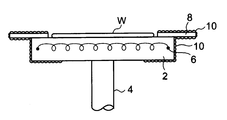
- FIG. 16 is a schematic configuration diagram showing a part of a conventional mounting table structure provided in the film forming apparatus.
- the mounting table 2 made of a ceramic material is supported by a column 4 erected from the bottom of the container. It is supported.
- a heater 6 is provided in the mounting table 2 so that the semiconductor wafer W mounted thereon is heated.
- a cover ring 8 having a ring shape is provided in the peripheral portion of the upper surface of the mounting table 2.
- not only the semiconductor wafer W but also the cover ring 8 as a component in the container and a part of the side surface and the lower surface of the mounting table 2 become high temperature. Will accumulate.
- an extra reaction by-product is generated and discharged together with the exhaust gas, and unreacted processing gas is also discharged.
- a trap mechanism is generally provided in the exhaust system extending from the processing vessel, thereby capturing reaction by-products and unreacted processing gas contained in the exhaust gas. To remove it. Unnecessary adhesion films adhering to the above components are removed, for example, by dry cleaning using a periodic chlorine-based or fluorine-based etching gas, or by wet cleaning performed by removing the components from the processing container. It is now discarded.
- the trap mechanism when removing reaction by-products that condense (liquefy) and solidify (solidify) at room temperature, the trap mechanism has, as an example, a large number of fins provided in a housing having an exhaust gas inlet and outlet. It has a configuration. In this case, the fins are sequentially arranged in the flow direction of the exhaust gas, and when the exhaust gas passes between these fins, reaction by-products in the exhaust gas adhere to the fin surface and are captured. It has become so. In addition, the trapping efficiency is increased by cooling these fins with a cooling medium or the like (see, for example, JP-A-2001-214272).
- a thin film is formed using a raw material (source gas) of an organometallic compound containing a noble metal such as silver, gold or ruthenium. Forming with an apparatus is also performed. Even in such a case, the exhaust gas is cooled, the gas is condensed, and the by-product including the unreacted raw material is recovered, and further, the unreacted raw material is obtained by purifying the by-product.
- source gas source gas
- the exhaust gas is cooled, the gas is condensed, and the by-product including the unreacted raw material is recovered, and further, the unreacted raw material is obtained by purifying the by-product.
- An object of the present invention is to reduce the number of dry cleaning processes, or to eliminate the dry cleaning process itself and to recover the raw material itself and the metal contained in the raw material efficiently and at low cost.
- An object is to provide a mounting table structure, a film forming apparatus, and a raw material recovery method.
- the present invention provides a mounting for mounting a target object in order to form a thin film on the surface of the target object using a raw material gas made of an organometallic compound in a processing container that can be evacuated.
- the mounting base body on which the object to be processed is mounted and a heater is provided, and the side surface and the bottom surface of the mounting base body are enclosed, and the mounting base body is supported, And a base that is maintained in a temperature range lower than the decomposition temperature of the raw material gas and equal to or higher than a solidification temperature or a liquefaction temperature.
- the present invention it is possible to suppress the deposition of an unnecessary thin film on the base side, and it is possible to deposit the thin film only on a necessary portion on the surface of the object to be processed. Therefore, the number of dry cleaning processes can be suppressed, or the dry cleaning process itself can be eliminated, and the recovery of the raw material itself and the metal contained in the raw material can be performed efficiently and at low cost.
- the present invention places the object to be processed in order to form a thin film on the surface of the object to be processed using a raw material gas made of an organic metal compound material in a processing container that can be evacuated.
- a metal base provided with a mounting table main body on which the object to be processed is mounted and a heater is provided inside, and a refrigerant passage that supports the mounting table main body and flows a refrigerant therein.
- a base part and a peripheral part that is detachably provided on the outer peripheral side of the mounting table main body so as to surround the mounting table main body and that is adjusted to a temperature equal to or higher than the decomposition temperature of the source gas when forming a thin film. This is a mounting table structure.
- the source gas that has not contributed to the film formation on the object to be processed is actively pyrolyzed by the peripheral component being heated and deposited as an unnecessary thin film on the surface of the peripheral component. it can. Therefore, by removing the peripheral parts later, the metal contained in the raw material can be efficiently and inexpensively recovered from the peripheral parts. Furthermore, it is possible to reduce the load on the exhaust system.
- the present invention relates to a processing container capable of being evacuated in a film forming apparatus for performing a film forming process for forming a thin film on a surface of an object to be processed using a raw material gas made of an organic metal compound. 29.
- the mounting table structure according to any one of claims 1 to 28 for mounting the object to be processed, a gas introduction unit that introduces gas into the processing container, and the gas introduction unit.
- a source gas supply system for supplying the source gas, an exhaust system for exhausting the atmosphere in the processing vessel, and a trap mechanism for collecting and collecting unreacted source gas from the exhaust gas flowing through the exhaust system;
- a film forming apparatus comprising:
- the unreacted raw material gas is collected from the exhaust gas by the trap mechanism, the raw material is not consumed wastefully, and the number of times of the dry cleaning process is suppressed, or The dry cleaning process itself can be eliminated, and the raw material itself can be recovered efficiently and at low cost.
- the object to be processed is mounted on a mounting table structure in a processing container that can be evacuated, and a raw material gas made of an organic metal compound material is used on the surface of the object to be processed.
- the structure other than the component that heats the object to be processed by the mounting table structure and is directly placed and in contact with the object to be processed A film forming step of forming the thin film on the surface of the object to be processed in a state in which the temperature of the component is maintained at a low temperature that is lower than the decomposition temperature of the source gas and is equal to or higher than a solidification temperature or a liquefaction temperature; And a recovery step for recovering the raw material by solidifying or liquefying the unreacted raw material gas contained in the exhaust gas discharged from the container.
- the raw material is recovered from the unreacted raw material gas in the exhaust gas, the raw material is not consumed wastefully and the number of times of the dry cleaning process is suppressed, or the dry cleaning process itself This makes it possible to recover the raw material itself efficiently and at low cost.
- the object to be processed is mounted on a mounting table structure in a processing container that can be evacuated, and a raw material gas made of an organic metal compound material is used on the surface of the object to be processed.
- a raw material gas made of an organic metal compound material is used on the surface of the object to be processed.
- the outer periphery side of the component in which the object to be processed is heated by the mounting table structure and the object to be processed is directly placed and in contact
- a recovery step of recovering the raw material by solidifying or liquefying the unreacted raw material gas contained in the raw material recovery method is provided in the raw material recovery method.
- the raw material since the raw material is recovered from the unreacted raw material gas in the exhaust gas, the raw material is not wasted.
- the raw material gas that has not contributed to the film formation is actively pyrolyzed on the surfaces of the peripheral components and deposited as an unnecessary thin film, and this is recovered later, thereby improving the efficiency of the recovery of the raw material.
- the object to be processed is mounted on a mounting table structure in a processing container that can be evacuated, and a raw material gas made of an organic metal compound material is used on the surface of the object to be processed.
- a coating film forming step for forming a coating film on a detachable component part of the mounting table structure, and a component part on which the coating film is formed A mounting step of mounting and forming a mounting table structure; and a film forming step of forming a thin film on the surface of the target object in a state where the target object is mounted on the mounting table structure on which the component parts are mounted.
- a removal step of removing the component from the mounting structure after the film formation step, and a removal step of removing the thin film adhering to the component together with the coating film from the component A raw material recovery method, characterized in that it and a recovery step of recovering the metals contained in the raw material from the removed film.
- the metal contained in the raw material can be recovered efficiently and at low cost.
- the object to be processed is mounted on a mounting table structure in a processing container that can be evacuated, and a raw material gas made of an organic metal compound material is used on the surface of the object to be processed.
- a mounting table structure is formed by mounting peripheral components on a mounting table main body provided with a heater so as to surround an outer peripheral side of the mounting table main body.
- the object to be processed is placed on the mounting table structure where the peripheral parts are mounted, and the object to be processed and the peripheral parts are maintained at a temperature equal to or higher than the decomposition temperature of the source gas.
- the present invention it is possible to efficiently and inexpensively recover the metal contained in the raw material from an unnecessary thin film deposited on the surface of the peripheral component, and also reduce the load on the exhaust system. It becomes possible.
- FIG. 1 It is a schematic block diagram which shows 1st Example of the film-forming apparatus which has the mounting base structure based on this invention. It is an expanded sectional view which shows 1st Example of a mounting base structure. It is an exploded sectional view showing details of a mounting base structure. It is the elements on larger scale which expanded a part of 1st Example of a mounting base structure. It is a graph which shows the relationship between semiconductor wafer temperature and a film-forming rate. It is a flowchart which shows 1st Example of the raw material collection
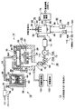
- FIG. 1 is a schematic configuration diagram showing a first embodiment of a film forming apparatus having a mounting table structure according to the present invention
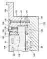
- FIG. 2 is an enlarged sectional view showing a first embodiment of the mounting table structure
- FIG. 4 is an exploded sectional view showing details of the mounting table structure
- FIG. 4 is a partially enlarged sectional view of a part of the first embodiment of the mounting table structure
- FIG. 5 is a graph showing the relationship between the semiconductor wafer temperature and the film formation rate. It is.
- Ru 3 (CO) 12 which is a carbonyl-based organometallic compound is used as a raw material for the organometallic compound, and CO (carbon monoxide) is used as a carrier gas to form a thin film made of a Ru metal film.
- CO carbon monoxide
- a film forming apparatus 12 includes a film forming apparatus main body 14 that actually performs a film forming process on a disk-shaped semiconductor wafer W as an object to be processed, and this film forming apparatus.
- the apparatus main body 14 is mainly composed of a source gas supply system 16 for supplying a source gas for film formation to an apparatus main body 14 and an exhaust system 18 for discharging exhaust gas from the film formation apparatus main body 14.
- the film forming apparatus main body 14 includes a cylindrical processing container 20 made of, for example, an aluminum alloy.
- a mounting table structure 22 according to the present invention is provided for mounting and holding a semiconductor wafer W as an object to be processed.
- the entire mounting table structure 22 is formed into a disk shape, for example, and the semiconductor wafer W is mounted on the upper surface side.
- the mounting table structure 22 is attached and fixed to an upper end portion of a metal column 24 made of, for example, an aluminum alloy that is erected from the bottom of the processing vessel 20.
- a heater 26 made of, for example, a tungsten wire heater or a carbon wire heater is embedded as a heating means on the upper side thereof, and the semiconductor wafer W is heated.
- a refrigerant passage 28 is provided below the heater 26, for flowing a refrigerant that cools the lower part and the side part of the mounting table structure 22 to adjust the temperature. Further details of the mounting table structure 22 will be described later. Further, the mounting table structure 22 is provided with a lifter pin (not shown) that is moved up and down when the semiconductor wafer W is carried in and out and transfers the semiconductor wafer W to and from the transfer arm.
- An exhaust port 30 is provided at the bottom of the processing container 20, and an exhaust system 8 is connected to the exhaust port 30 so that the atmosphere in the processing container 20 can be evacuated.
- the exhaust system 18 will be described later.
- An opening 32 for loading and unloading the semiconductor wafer W is formed on the side wall of the processing container 20, and a gate valve 34 for opening and closing the opening 32 is provided in the opening 32.
- a gas introducing means 38 including a shower head 36 is provided on the ceiling of the processing container 20, and a necessary gas is supplied into the processing container 20 from a gas ejection hole 40 provided on the lower surface. ing. Heaters 42 and 44 are provided on the side wall of the processing vessel 20 and the shower head 36, respectively, and by maintaining these at a predetermined temperature, the source gas is prevented from solidifying or liquefying. .
- the raw material gas supply system 16 and, if necessary, other gas is connected to the gas inlet 36A of the shower head 36, the gas supply system is connected.
- the raw material gas and other gases may be mixed in the shower head 36, or may be separately introduced into the shower head 36 and flow separately before being mixed in the processing vessel 20. In some cases.
- the shower head 36 is used as the gas introduction means 38, but instead of this, a simple nozzle or the like may be used, and the gas introduction mode is not particularly limited.
- the source gas supply system 16 has a source tank 46 for storing a solid source or a liquid source.
- a solid raw material 48 which is a raw material of the organometallic compound is stored.
- Ru 3 (CO) 12 is used as the solid material 48.
- This solid material 48 generally has a characteristic that vapor pressure is very low and it is difficult to evaporate.
- a liquid material in which a material gas is formed by bubbling or the like may be used.
- One end of the raw material passage 52 is connected to the gas outlet 50 provided in the ceiling portion of the raw material tank 46, and the other end of the raw material passage 52 is connected to the gas inlet 36 ⁇ / b> A of the shower head 36 of the film forming apparatus main body 14. Thereby, the raw material gas generated in the raw material tank 46 can be appropriately supplied.
- An opening / closing valve 54 is interposed in a portion of the raw material passage 52 close to the raw material tank 46.
- a carrier gas pipe 56 for supplying a carrier gas to the raw material tank 46 is connected to the lower surface side of the raw material tank 46.
- a flow rate controller 58 such as a mass flow controller and a carrier gas on / off valve 60 are sequentially provided.
- a porous plate 62 is installed in the vicinity of the side where the carrier gas pipe 56 is installed.
- the solid material 48 is held on the porous plate 62.
- the carrier gas supplied from the carrier gas pipe 56 is uniformly supplied into the raw material tank 46 through the holes formed in the porous plate 62.
- CO (carbon monoxide) gas is used as the carrier gas.
- the raw material tank 46 is provided with tank heating means 64 for heating it so as to cover the entire tank. Thereby, vaporization of the solid raw material 48 is accelerated
- the heating temperature of the solid raw material 48 is lower than the decomposition temperature of the raw material gas and higher than the solidification temperature.
- the raw material passage 52 is provided with a passage heater 66 such as a tape heater, and the raw material gas is regenerated by heating the raw material passage 52 to a temperature lower than the decomposition temperature of the raw material gas and higher than the solidification temperature. Solidification is prevented.
- the exhaust system 18 has an exhaust passage 68 connected to the exhaust port 30 of the processing container 20, and the atmosphere in the processing container 20 is exhausted along the exhaust passage 68. Specifically, in this exhaust passage 68 from the upstream side to the downstream side, the pressure regulating valve 70, the vacuum pump part 72, the auxiliary trap mechanism 74 and the main trap mechanism 76 which are trap mechanisms, and the detoxification A device 78 is sequentially provided.
- the pressure adjustment valve 70 is made of a butterfly valve, for example, and has a function of adjusting the pressure in the processing container 20.
- the vacuum pump unit 72 includes a turbo molecular pump 72A provided on the upstream side and a dry pump 72B provided on the downstream side, so that the atmosphere in the processing vessel 20 can be evacuated. In this case, only one of the two pumps 72A and 72B may be provided according to the set process pressure at the time of film formation.
- the auxiliary trap mechanism 74 cools the flowing exhaust gas and collects the unreacted source gas contained in the exhaust gas.
- the auxiliary trap mechanism 74 is provided in the front stage of the main trap mechanism 76 and is not yet reacted. A part of the raw material gas is recovered. This is particularly effective when there is a large amount of unreacted source gas or when the recovery capability of the main trap mechanism 76 at the subsequent stage is not sufficiently large. In other words, the auxiliary trap mechanism 74 may not be provided when the amount of unreacted source gas is small or when the recovery capability of the main trap mechanism 76 at the subsequent stage is sufficiently large.
- a cryopump having a cryopanel made at a very low temperature can be used. By this cryopanel, unreacted source gas is cooled and adsorbed.
- the main trap mechanism 76 cools the exhaust gas and collects the unreacted source gas contained in the exhaust gas.
- the unreacted source gas that is, Ru 3 is used. (CO) Almost all of the 12 gases are recovered.
- the main trap mechanism 76 is cooled by contacting exhaust gas with a refrigerant to solidify unreacted raw material gas and reprecipitate the raw material, and reprecipitates by filtering the refrigerant in the solidifying unit 80. And a filtration / recovery unit 82 for separating the recovered raw material from the refrigerant and recovering it.
- the coagulation unit 80 is made of, for example, a scrubber device and has a coagulation container 84 formed in a cylindrical shape.
- a gas inlet 86 is provided at the upper part of the side wall of the coagulation vessel 84, and one side of the exhaust passage 68 is connected to the gas inlet 86, and the central part of the side wall facing the gas inlet 86, or a little lower than that.
- a gas outlet 88 is provided on the side, and the other side of the exhaust passage 68 is connected to the gas outlet 88.
- the exhaust gas flows into the coagulation vessel 84 from the gas inlet 86 and flows out from the gas outlet 88.
- a baffle plate or the like may be appropriately provided in the coagulation vessel 84 so that the path length through which the exhaust gas flows in the coagulation vessel 84 may be set longer.
- a shower head 92 having a plurality of nozzles 92A is provided on the ceiling portion side in the coagulation vessel 84, and a liquid supply pipe 94 is connected to the shower head 92 so that a refrigerant flows through it. It has become. Therefore, in the coagulation vessel 84, the refrigerant is discharged in a shower shape from each nozzle 92A of the shower head 92, and the exhaust gas is cooled by contacting the refrigerant with the exhaust gas.
- this refrigerant a refrigerant that is insoluble or hardly soluble in the raw material, for example, cooling water is used here.
- the unreacted raw material gas in the exhaust gas is solidified by cooling with the refrigerant, and Ru 3 (CO) 12 as the raw material is reprecipitated.
- the reason why cooling water is used as the refrigerant is that Ru 3 (CO) 12 does not decompose with respect to the cooling water (water) and has stable characteristics.
- a liquid outlet 96 and a liquid inlet 98 are provided at the bottom of the coagulation vessel 84.
- the filtration recovery unit 82 is provided in the circulation passage 100 connected to connect the liquid outlet 96 and the liquid inlet 98.
- a circulation pump 102 is provided in the middle of the circulation passage 100, and the refrigerant containing the re-deposited raw material in the coagulation vessel 84 is circulated in the circulation passage 100.
- a recovery container 104 for recovering the re-deposited raw material from the refrigerant is provided upstream of the circulation pump 102 in the circulation passage 100.
- a filter 106 is provided in the collection container 104 so as to be replaceable. By filtering the refrigerant with the filter 106, the re-deposited raw material can be recovered.
- a discharge pipe 110 having a discharge opening / closing valve 108 provided in the middle is branched from the circulation passage 100 between the circulation pump 102 and the collection container 104. Thereby, excess refrigerant can be discharged out of the system as necessary.
- a passage heater such as a tape heater is provided in the exhaust passage 68 from the exhaust port 30 of the processing vessel 20 to the main trap mechanism 76 and each member (including the vacuum pump unit 72) interposed in the middle thereof. 112 is provided.
- the exhaust gas flowing in the exhaust passage 68 is heated to a predetermined temperature, and unreacted source gas in the exhaust gas is prevented from being liquefied or solidified in the middle.
- the auxiliary trap mechanism 74 When the exhaust passage 68 from the exhaust port 30 of the processing container 20 to the main trap mechanism 76 may be a problem, for example, when the installation cost of the passage heater 112 may be a problem, the auxiliary trap mechanism 74 and If the main trap mechanism 76 is provided between the pressure regulating valve 70 and the turbo molecular pump 72A, or provided between the turbo molecular pump 72A and the dry pump 72B, the main trap mechanism 76 is provided downstream of the main trap mechanism 76.
- the passage heater 112 can be omitted, and the laying range of the passage heater 112 can be shortened.
- the abatement device 78 provided on the downstream side of the main trap mechanism 76 renders harmful gas in the exhaust gas harmless.
- CO carbon monoxide
- the abatement device 78 burns these CO, for example, to produce CO 2. It is detoxified as (carbon dioxide) and released into the atmosphere.
- the mounting table structure 22 includes the heater 26 and the refrigerant passage 28.
- the mounting table structure 22 includes a mounting table main body 114 on which a semiconductor wafer W is mounted and a heater 26 is provided, and the mounting table.
- a temperature range that is lower than the decomposition temperature of the raw material gas and equal to or higher than the solidification temperature or the liquefaction temperature is provided with a refrigerant passage 28 that supports the mounting table main body 114 in a state of surrounding the side surface and bottom surface of the main body 114 and flows the refrigerant therein.
- a base 116 that is maintained at the same time.
- the mounting table main body 114 is entirely formed into a disk shape from a ceramic material, metal, or the like, and the heating heater 26 made of tungsten, wire heater, carbon wire, or the like is insulated over the entire surface as a heating means.
- the semiconductor wafer W which is embedded in a state and is directly placed on and in contact with the upper surface, can be heated to a desired temperature to control the temperature.
- the diameter of the mounting table main body 114 is set slightly smaller than the diameter of the semiconductor wafer W. For example, when the diameter of the semiconductor wafer W is 300 mm, the diameter of the mounting table main body 114 is set to about 295 mm.
- a stepped portion 118 (see FIG. 3) having a cross section cut off at a right angle is formed in a ring shape along the circumferential direction of the peripheral portion of the mounting table main body 114.
- the base 116 is entirely made of metal.
- the base 116 includes a disk-shaped metal base portion 120 in which the refrigerant passage 28 is provided over substantially the entire surface, and the side surface of the mounting table main body 114 is surrounded by a peripheral portion of the base portion 120.
- the ring-shaped metal edge ring 122 provided so as to stand up is mainly constituted. Cooling water, Fluorinert, Galden (registered trademark), or the like as a refrigerant flows through the refrigerant passage 28 via a pipe (not shown).
- edge ring 122 Between the base part 120 and the edge ring 122, in order to alleviate the cooling of the edge ring 122, a ring-shaped heat made of a metal having a lower thermal conductivity than the metal constituting the edge ring 122 and the base part 120.
- a conduction relaxation member 124 is interposed.
- these edge ring 122, the heat conduction relaxation member 124, and the base part 120 are integrally couple
- the base portion 120 and the edge ring 122 are each made of aluminum or an aluminum alloy, and the heat conduction relaxation member 124 is made of stainless steel having a thermal conductivity inferior to that of aluminum or an aluminum alloy. However, since the heat conduction relaxation member 124 may be provided as necessary, it can be omitted.
- the base 120 and the edge ring 120 may be made of stainless steel, although the thermal conductivity is slightly inferior to aluminum or aluminum alloy.
- heat insulating materials 128 and 129 are interposed between the upper surface of the base portion 120 and the bottom portion (lower surface) of the mounting table main body 114. In such a state, the mounting table main body 114 is supported, so that heat insulation between them is achieved.
- the heat insulating materials 128 and 129 a ceramic material or stainless steel having low heat conductivity and excellent heat resistance can be used.
- These heat insulating materials are composed of a ring-shaped heat insulating material 128 that supports the outer periphery of the bottom of the mounting table main body 114 and a plurality of small heat insulating materials 129 that support the inner periphery of the bottom portion. The presence of the plurality of space portions 130 between them improves heat insulation (see FIG. 4).
- these heat insulating materials have support protrusions 132A and 133A formed at the upper portion and leg portions 132B and 133B formed at the lower portion so that the contact area (heat transfer area) is made as small as possible. Yes. Thereby, the heat insulation is further improved.
- a flat portion is formed at the tips of the heat insulating support protrusions 132A and 133A, and the radial length of the flat portion a of the ring-shaped heat insulating material 128 is the radial length of the flat portion b of the small piece of heat insulating material 129. For example, the atmosphere of the processing space is effectively prevented from entering the space 130.
- the upper surface of the edge ring 122 extends by a predetermined length outward in the radial direction of the semiconductor wafer W while maintaining substantially the same level as the horizontal level of the mounting surface of the semiconductor wafer W.
- a ring-shaped flange portion 134 is formed. Thereby, the source gas flowing from above to the periphery of the semiconductor wafer W is guided to the semiconductor wafer W side, so that efficient film formation is performed.
- a protrusion 136 protruding toward the inner peripheral side is provided in a ring shape along the circumferential direction on the inner peripheral side of the edge ring 122.
- the protrusion 136 extends partway through the stepped portion 118 of the mounting table main body 114.
- the projection 136 is provided with a fixing screw 138 so as to penetrate from the upper side to the lower side. By advancing the fixing screw 138 downward, the peripheral portion of the mounting table main body 114 is pressed and the mounting table main body 114 is fixed.
- the inner peripheral surface of the edge ring 122 and the outer peripheral surface of the mounting table main body 114 are not in direct contact with each other, and a space portion 140 for heat insulation remains between them. Further, only about six fixing screws 138 are provided as a whole, and this also improves the heat insulation between the edge ring 122 and the mounting table main body 114.
- a ring-shaped shield ring 142 is detachably provided in a loosely fitted state between the upper side surface of the stepped portion 118 of the mounting table main body 114 and the inner peripheral surface of the protruding portion 136 of the edge ring 122. Yes. Therefore, the shield ring 142 is a component that is detachable from the processing container 20.
- the shield ring 142 is made of a metal such as aluminum or an aluminum alloy, prevents film formation on the side wall of the mounting table main body 114, ensures in-plane temperature uniformity of the semiconductor wafer W, and prevents film formation on the back surface of the semiconductor wafer W. In addition, it performs functions such as heat insulation between the mounting table main body 114 and the edge ring 122.
- the computer-readable program necessary for this control is stored in the storage medium 152.
- a flexible disk CD (Compact Disc), CD-ROM, hard disk, flash memory, DVD, or the like is used.
- FIG. 6 is a flowchart showing a first embodiment of the raw material recovery method of the present invention.
- the turbo molecular pump 72 ⁇ / b> A and the dry pump 72 ⁇ / b> B of the vacuum pump unit 72 of the exhaust system 18 are continuously driven to Is evacuated and maintained at a predetermined pressure.
- the semiconductor wafer W supported on the mounting table structure 22 is maintained at a predetermined temperature by the heater 26, and the side wall of the processing vessel 20 and the shower head 36 are also heated at different predetermined temperatures by the heaters 42 and 44, respectively.
- the latter predetermined temperature is a temperature that is lower than the decomposition temperature of the source gas and within the range of the solidification temperature or liquefaction temperature of the source gas, and is about 80 ° C., for example.
- the entire raw material gas supply system 16 is heated in advance to a predetermined temperature, for example, about 80 ° C. as described above, by the tank heating means 64 and the passage heater 66.
- a predetermined temperature for example, about 80 ° C. as described above.
- the carrier gas (CO) whose flow rate is controlled is supplied into the source tank 46 through the carrier gas pipe 56 and stored in the source tank 46.
- the solid raw material 48 that is being heated is vaporized to generate a raw material gas.
- the raw material gas generated in this way flows in the raw material passage 52 toward the downstream side together with the carrier gas.
- This source gas is introduced from the shower head 36 of the film forming apparatus main body 14 into the processing container 20 in a reduced pressure atmosphere.
- a Ru metal thin film is formed on the semiconductor wafer W by, for example, CVD (Chemical Vapor Deposition) in the processing vessel 20.
- CVD Chemical Vapor Deposition
- the film-forming process S1 shown in FIG. 6 is performed.
- the process conditions at this time are such that the process pressure is about 0.1 Torr (13.3 Pa) and the semiconductor wafer temperature is equal to or higher than the decomposition temperature of the source gas, for example, about 150 to 250 ° C. As shown in FIG.
- Ru 3 (CO) 12 that is the solid raw material 48 is a raw material that has a very low vapor pressure and is difficult to evaporate (vaporize). Further, the amount (ratio) contributing to the film forming reaction is very small, and about 90% of the raw material gas flows down in the exhaust passage 68 of the exhaust system 18 together with the carrier gas CO in an unreacted state.
- the exhaust passage 68 is also heated to about 80 ° C. by the passage heater 112 as described above, and the raw material gas is prevented from re-solidifying.
- the film formation reaction is represented by the following chemical formula, and CO (carbon monoxide), which is the same gas type as the carrier gas, is generated.
- the exhaust gas flowing down the exhaust passage 68 is sequentially diffused into the atmosphere after passing through the pressure regulating valve 70, the turbo molecular pump 72A, the dry pump 72B, the auxiliary trap mechanism 74, the main trap mechanism 76, and the abatement device 78. .
- the CO gas is abated by combustion in the abatement device 78 and becomes CO 2 and then the atmosphere. Dissipated.
- the auxiliary trap mechanism 74 composed of, for example, a cryopump
- the exhaust gas is cooled by the cryopanel, and a part of the unreacted source gas is condensed (solidified), and reprecipitated. Is recovered by adhering to the cryopanel.
- the exhaust gas flowing out of the auxiliary trap mechanism 74 flows into the main trap mechanism 76 and comes into contact with the refrigerant. As a result, almost all unreacted source gas is recovered. Thereby, the collection step S2 in FIG. 6 is performed.
- exhaust gas is brought into contact with a refrigerant and cooled to solidify unreacted raw material gas to reprecipitate the raw material, and the reprecipitated raw material is separated from the refrigerant and recovered. Done.
- the exhaust gas flowing into the coagulation vessel 84 from the gas inlet 86 is injected from each nozzle 92A of the shower head 92 provided on the ceiling. It is cooled by contact, and then discharged from the gas outlet 88.
- the cooling water when the exhaust gas is cooled in contact with the refrigerant, here, the cooling water, the unreacted source gas contained in the exhaust gas is also cooled and condensed (or solidified), and the source material is re-deposited. Will do.
- the temperature of the cooling water depends on the vaporization temperature (sublimation temperature) of the raw material and the like, but is preferably about 0 to 30 ° C., for example.
- the re-deposited raw material accumulates at the bottom of the coagulation vessel 84 together with the refrigerant (cooling water).
- the carrier gas, CO hardly dissolves in the cooling water.
- the refrigerant in the coagulation vessel 84 flows out from the liquid outlet 96 into the circulation passage 100 when the circulation pump 102 of the filtration recovery unit 82 is driven, and flows through the circulation passage 100 and then the liquid inlet 98. Is returned to the coagulation vessel 84, that is, circulated. In this case, the refrigerant flowing through the circulation passage 100 flows through the collection container 104.
- a plurality of recovery containers 104 may be provided in parallel so that they can be switched and used. Further, since the recovered raw material is not contaminated with impurities, there is no need to purify it. That is, after drying this, it can be used as the solid raw material 48 in the raw material tank 46 as it is. Analysis of the raw material actually recovered revealed that Ru as a metal, Ru 3 (CO) 12-X as an intermediate product, etc. were not detected, and the total amount was Ru 3 (CO) 12 .
- the semiconductor wafer W is heated to a high temperature of about 150 to 250 ° C., for example, about 190 to 230 ° C. This means that the semiconductor wafer W of the mounting table structure 22 is directly heated. It means that the mounting table main body 114 to be mounted is heated to a corresponding high temperature state by the heater 26 incorporated therein.
- the base 116 that supports the mounting table main body 114 has a temperature lower than the decomposition temperature of the raw material gas and equal to or higher than the solidification temperature or liquefaction temperature of the raw material gas, for example, by flowing cooling water through the refrigerant passage 28. It is maintained at a low temperature of about 80 to 110 ° C.
- the decomposition temperature of the raw material gas is about 150 ° C.
- the solidification temperature is about 75 ° C.
- the temperature of the base portion 120 of the base 116 is maintained at about 80 ° C.
- the temperature of the edge ring 122 surrounding the side surface of the mounting table main body 114 is maintained at about 100 ° C.
- the temperature of these components including the heat conduction relaxation member 124 interposed therebetween is set to be lower than the thermal decomposition temperature of the raw material gas. Accordingly, it is possible to effectively prevent an unnecessary thin film of the Ru film from being deposited on the surface of these constituent members.
- the space between the mounting table main body 114 and the base portion 120 is insulated by the heat insulating materials 128 and 129 and the space portion 130, and the space between the mounting table main body 114 and the edge ring 122 is also insulated by the space portion 140. Therefore, even if the temperature of the mounting table main body 114 is as high as about 190 to 230 ° C., the base portion 120, the edge ring 122, and the heat conduction relaxation member 124 that support it can be efficiently cooled. As a result, unnecessary thin films are effectively prevented from being deposited on the surfaces of these components as described above.
- the thermal conduction relaxation member 124 is interposed between the edge ring 122 and the base portion 120 so that the temperature of the edge ring 122 becomes higher than the temperature of the base portion 120.
- the ring-shaped shield ring 142 interposed between the edge ring 122 and the mounting table main body 114 is adjacent to the high-temperature mounting table main body 114 on the inner side, so that it is equal to or higher than the pyrolysis temperature of the source gas. As the temperature rises, an unnecessary thin film is deposited on the upper surface side of the shield ring 142, but the amount of the thin film deposited on the upper surface is small.
- a thin film is deposited only on a necessary portion of the surface of the semiconductor wafer W, and unnecessary thin films are deposited on the surfaces on the base 116 side such as the edge ring 122, the base portion 120, and the heat conduction relaxation member 124. Since it was devised not to make it, the raw material gas is not consumed on the surface of the latter part and flows to the exhaust system 18 in an unreacted state, and is recovered as a raw material in the recovery step S2 described above. Further, as described above, the fact that unnecessary thin films are not deposited makes it possible to reduce or eliminate the need for dry cleaning.
- a thin film for example, a Ru metal film is applied to the semiconductor wafer W, which is an object to be processed, using a source gas of an organometallic compound, for example, Ru 3 (CO) 12 gas, in the processing container 20.
- a source gas of an organometallic compound for example, Ru 3 (CO) 12 gas
- a base 116 that is provided with a refrigerant passage 28 that allows a refrigerant to flow therein and is maintained at a temperature lower than the decomposition temperature of the raw material gas and higher than the solidification temperature or liquefaction temperature of the raw material gas.
- the deposition of an unnecessary thin film on the base 116 side is suppressed, and the deposition of the thin film only on the necessary portion that is the surface of the object to be processed is promoted.
- the number of dry cleaning processes can be suppressed, or the dry cleaning process itself can be eliminated. Further, the recovery of the raw material itself and the metal contained in the raw material can be performed efficiently and at low cost.
- the temperature of the base 116 is set to a temperature range lower than the decomposition temperature of the raw material gas and equal to or higher than the solidification temperature or liquefaction temperature of the raw material gas, and is not required on the surface of the base 116.
- the inner peripheral side of the upper surface of the edge ring 122 of the mounting table structure 22 and the shield ring 142 An unnecessary thin film 160 made of a Ru film thin film may adhere to the upper surface.
- the temperature of the edge ring 122 may be increased to an intermediate temperature of about 150 to 180 ° C. In that case, the tendency of the unnecessary thin film 160 to adhere to the inner peripheral side of the upper surface of the edge ring 122 is increased.
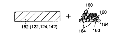
- FIG. 8A to FIG. 8C are schematic diagrams showing changes in the components on which the coating film is formed when the second embodiment of the raw material recovery method of the present invention is performed, and FIG. 9 shows the raw material recovery method of the present invention. It is a flowchart which shows 2nd Example.
- the detachable component part of the mounting table structure 22, that is, the replaceable component part is removed, and the surface of the component part 162 is coated as shown in FIG. 8A.
- a film 164 is formed. That is, a coating film forming step is performed (S11 in FIG. 9).
- the edge ring 122, the heat conduction relaxation member 124, and the shield ring 142 in the mounting table structure 22 correspond to the component parts 162 that are detachable.
- the coating film 164 may be formed on the entire surface of the component 162, but may be formed on only a part of the surface. However, it is preferable to cover at least a portion exposed to the atmosphere in the processing container 20 (a portion where an unnecessary thin film 160 (see FIG. 7) may be deposited).
- the coating film 164 it is preferable to use a coating film that does not have good adhesion to the component 160 (can be peeled off) and is easy to peel off.
- the coating film 164 an aluminum sprayed film, a Teflon (registered trademark) film, or the like can be used.
- the edge ring 122, the heat conduction relaxation member 124, and the shield ring 142, which are the component 162 described above, are formed of metal such as aluminum, aluminum alloy, stainless steel, or the like, but the component 162 is made of alumina or nitride. Even when formed of a ceramic material such as aluminum, it is effective to form the coating film 164.
- the mounting step S12 is performed by mounting and mounting the component 162 as the mounting table structure 22.
- the edge ring 122, the heat conduction relaxation member 124, and the shield ring 142, which are the component parts 162 are assembled as shown in FIG. 2, and the mounting table structure 22 is completed.
- a film forming process is performed by flowing a raw material gas into the processing container 20 to form a thin film made of a Ru film (S13).
- this film forming step S13 is repeated, an unnecessary thin film 160 made of a Ru film is deposited and deposited on the surface of each component 162 as shown in FIG. 8B.
- the first embodiment of the raw material recovery method is also performed in parallel and the raw material itself is recovered.
- the mounting table structure 22 is then disassembled, and the edge ring 122, the heat conduction relaxation member 124, and the shield ring 142, which are the component parts 162, are removed.
- a removal process is performed (S14).
- a removal step is performed to remove the unnecessary thin film 160 adhering to the surface of the removed edge ring 122, heat conduction relaxation member 124, and shield ring 142 together with the coating film 164 (S15).
- a recovery step of recovering the removed unnecessary thin film 160 is performed (S16).
- unnecessary thin film 160 and coating film 164 can be integrally peeled off by physical collision, for example, by collision by sandblasting.
- the coating film 164 is aluminum sprayed, since the Ru film is resistant to acids and alkalis, the coating of aluminum spraying is performed by acting hydrochloric acid, ammonia, sodium hydroxide, etc.
- the unnecessary thin film 160 can be peeled off.
- the coating film 164 is formed again on the component 162 from which the coating film 164 has been removed (S11) and reused.
- a regeneration process for regenerating Ru 3 (CO) 12 as a raw material is performed by subjecting the Ru metal to, for example, carbonylation treatment ( S17).
- the metal contained in the raw material, such as Ru can be recovered efficiently and at low cost.
- the semiconductor wafer W is mounted as the object to be processed on the mounting table structure in the processing container 20 that can be evacuated, and the organometallic compound is formed.
- a raw material recovery method in a film forming apparatus in which a thin film is formed on the surface of an object to be processed using a raw material gas made of a raw material, a coating film 164 is formed on a component 162 (122, 124, 142) having a mounting table structure. Then, by removing unnecessary thin films adhering to the components together with the coating film after the film formation from the components, the metal contained in the raw material, such as Ru, can be recovered efficiently and at low cost.
- a film is formed on the bevel portion, which is the end surface of the semiconductor wafer W, on the upper surface side of the edge ring 122 that forms a part of the base 116 as in the modification of the mounting table structure shown in FIG.
- a ring-shaped cover ring 170 may be provided in order to prevent adhesion.
- the cover ring 170 is made of a ceramic material such as alumina or aluminum nitride, and is configured as a detachable component 162.
- the temperature of the cover ring 170 is also maintained at a temperature range lower than the decomposition temperature of the source gas and equal to or higher than the solidification temperature or liquefaction temperature of the source gas.
- the coating film 164 of the second embodiment of the method of the present invention can also be applied to a component 162 that is detachable from a mounting table mechanism that does not have a cooling mechanism.
- the refrigerant and the raw material gas are brought into direct contact.
- the refrigerant is connected to the cooling pipe. It is desirable to adopt a configuration in which, when the raw material gas is cooled and reliquefied in such a manner that the refrigerant and the raw material gas are not in direct contact with each other, the two are not mixed.
- FIG. 11 is a schematic sectional view showing a film forming apparatus main body used in the second embodiment of the film forming apparatus of the present invention.
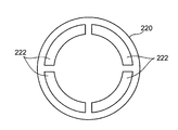
- FIG. 12 is a plan view showing an example of a baffle plate used in the film forming apparatus main body.
- the mounting table structure other components excluding the mounting table main body 114 and the shield ring 142, such as the base 120, the edge ring 122, the heat conduction reducing member 124, and the cover.
- the ring 170 was set to a temperature range lower than the decomposition temperature of the raw material gas and higher than the solidification temperature or liquefaction temperature of the raw material gas so that unnecessary thin film 160 did not adhere.
- the temperature of the edge ring 122 and the cover ring 170 which are peripheral components is set to a temperature equal to or higher than the decomposition temperature of the source gas except for the base portion 120. And it intends to collect
- the processing container 20 includes an upper chamber having a larger inner diameter and a lower chamber having a smaller inner diameter.
- An exhaust space 200 is formed.
- An exhaust port 30 is formed in the lower side wall that defines the exhaust space 200 as the lower chamber, and the exhaust system 18 as described above is connected to the exhaust port 30.
- pillar 24 of the mounting base structure 22 of 2nd Example penetrates the bottom part which divides the said exhaust space 200, is extended below, and is connected to the actuator which is not shown in figure. Thereby, the whole mounting table structure 22 can be moved up and down in the vertical direction, and can be stopped at an arbitrary position.
- a metal bellows 202 that can be expanded and contracted is provided in a portion through which the column 24 penetrates. Thereby, the mounting table structure 22 can be raised and lowered while maintaining the airtightness in the processing container 20.
- a plurality of, for example, three (only two are shown in the figure) pin insertion holes 206 are provided in the periphery of the mounting table 204 including the base 116 and the mounting table main body 114.
- a lifter pin 208 can be inserted into each pin insertion hole 206.
- the lower end part of each lifter pin 208 is supported by the raising / lowering arm 210, and the said raising / lowering arm 210 is connected to the raising / lowering rod 214 which penetrates the container bottom part airtightly via the bellows 212, and can raise / lower. Yes.
- the lifter pins 208 can be raised and lowered above the mounting table 204 while the mounting table 204 is lowered to the transfer position of the wafer W, so that the wafer W can be pushed up and down.
- the opening 32 and the gate valve 34 are provided in the container side wall corresponding to the horizontal level of the upper surface of the mounting table 204 in the lowered position.
- a gas inlet 36 ⁇ / b> A to which a raw material gas supply system 16 and a gas supply system for supplying other necessary gas are connected is formed at the center of the ceiling of the processing container 20.
- a gas introduction means 38 is provided in communication with the gas inlet 36A.
- the gas introduction means 38 has a configuration as disclosed in, for example, Japanese Patent Application Laid-Open No. 2009-239104.
- the gas introduction means 38 supplies the raw material gas to the outer portion as viewed in the radial direction from the semiconductor wafer W placed on the placement table structure 22 here. That is, the gas introduction part 216 is configured so that the source gas flows to a gas outlet described later while avoiding the wafer W.
- the gas introduction part 216 is formed by a cylindrical inner partition wall 218 having an inner diameter larger than the diameter of the wafer W, and a baffle plate 220 provided in the inner partition wall 218.
- the internal partition wall 218 is attached to the ceiling surface of the container, and the baffle plate 220 is attached above the inside of the cylindrical internal partition wall 218 so as to face the wafer W.
- the peripheral part of the baffle plate 220 is provided with a plurality of openings 222 formed in an arc shape over the entire circumference along the circumferential direction as shown in FIG. Therefore, the upper part of the baffle plate 220 functions as a diffusion chamber 224 in which the source gas diffuses, and the source gas flows down or is injected toward the processing space S below the openings 222.
- each opening 222 corresponds to a position outside the outer peripheral edge of the wafer W on the mounting table 204. That is, the portion immediately below each opening 222 corresponds to the outside of the outer peripheral edge of the wafer W. In this way, the surface of the film thickness on the wafer W is not caused by causing the source gas to flow to a region outside the peripheral edge of the wafer W without directly flowing the source gas to the upper surface of the wafer W. Inner uniformity is ensured.
- the internal partition wall 218 and the baffle plate 220 are made of a metal material having good thermal conductivity, such as aluminum or an aluminum alloy.
- the internal partition wall 218 is also used as the gas outlet forming component 226 here. That is, the gas outlet forming component 226 that is the internal partition wall 218 extends downward, and the lower end thereof approaches the peripheral edge of the mounting table 204 to form the gas outlet 228 for exhaust. It has become.
- the gas outlet 228 is formed in an annular shape along the circumferential direction of the mounting table 204.
- the flow path is narrowed by the gas outlet 228, and the source gas is uniformly exhausted from the outer peripheral side of the wafer W.
- the gas outlet forming component 226 that defines the gas outlet 228 is positioned above the flange portion 134 and the cover ring 170 located at the peripheral edge of the mounting table 204, and the upper surface (flange portion) of the cover ring 170.
- the gas outlet 228 is formed between the gas outlet forming part 226 and the lower end surface of the gas outlet forming part 226.
- a ring-shaped projection 230 is formed along the circumferential direction at the lower end portion of the gas outlet forming component 226.
- the vertical width L1 of the gas outlet 228 is set within a range of 1 to 10 mm, for example, about 2 mm.
- peripheral components 232 that are detachably provided on the outer peripheral side of the mounting table main body 114 so as to surround the mounting table main body 114 have a temperature equal to or higher than the decomposition temperature of the source gas at the time of thin film formation.
- the temperature is set.
- the peripheral component 232 is a component provided on the outer peripheral side of the mounting table main body 114 among the components described in the first embodiment.
- the shield ring 142 and a part of the base 116 are provided.
- the edge ring 122 and the cover ring 170 constituting the above correspond to the peripheral component 232.
- the temperature of these parts is set to a low temperature so that unnecessary films are not deposited on the edge ring 122 and the cover ring 170 (see FIG. 10).
- the temperature of these components is increased.
- a part of the space 140 formed between the outer peripheral surface of the mounting table main body 114 and the inner peripheral surface of the edge ring 122 is heated to improve the thermal conductivity between the two.
- a conductivity facilitating member 234 is interposed so as to be in contact with both.
- the thermal conductivity promoting member 234 is formed, for example, in a ring shape along the circumferential direction of the mounting table main body 114, and the temperature on the edge ring 122 side made of aluminum or the like during film formation is substantially equal to the temperature of the mounting table main body 114.
- the temperature is the same as that of the decomposition temperature of the raw material gas.
- the temperature of the cover ring 170 made of a ceramic material such as alumina placed on the edge ring 122 is also substantially the same as that of the edge ring 122. Since the shield ring 142 is in direct contact with the mounting table main body 114 at the lower end thereof, the temperature is substantially the same as that of the mounting table main body 114.
- the thermal conductivity promoting member 234 a metal material having good thermal conductivity such as aluminum or an aluminum alloy can be used. From the beginning, if the protrusion is provided at the same position as the installation position of the thermal conductivity promoting member 234 on the mounting table main body 114 or the edge ring 122 side, the mounting table main body 114 and the edge ring 122 are directly connected to each other. It is not necessary to provide the thermal conductivity promoting member 234 in contact.
- the thermal conductivity promoting member 234 may be provided at any position within the space 140, and the installation position is not particularly limited. Although the case where the cover ring 170 is provided has been described here, there may be a case where the cover ring 170 is not provided as described in the first embodiment. Alternatively, other peripheral parts may be provided in addition to the cover ring 170. In any case, it is needless to say that the present embodiment can be applied.
- FIG. 14 is a flowchart showing a third embodiment of the raw material recovery method of the present invention.
- This raw material recovery method is basically the same as the method described with reference to the flowchart shown in FIG. 6 except that the temperature of the peripheral component 232 is different.
- the semiconductor wafer W supported on the mounting table structure 22 is maintained at a predetermined temperature by the heater 26.
- the inner partition wall 218 to the baffle plate 220 forming the side wall of the processing vessel 20 and the gas introduction means 38 are also maintained at different predetermined temperatures by the heaters 42 and 44, respectively.
- the latter temperature is a temperature lower than the decomposition temperature of the source gas and within the range equal to or higher than the solidification temperature or liquefaction temperature of the source gas, and is about 80 ° C., for example.
- the source gas generated in the source gas supply system 16 is introduced together with the carrier gas from the gas inlet 36A of the film forming apparatus main body 14 into the diffusion chamber 224 that forms the gas introduction part 216 of the gas introduction unit 38. Spread. Thereafter, the source gas flows downward from the openings 222 provided in the peripheral portion of the baffle plate 220 and flows into the processing space S in a reduced pressure atmosphere.
- This source gas flows in the processing space S while partly diffusing toward the center of the wafer W.
- the atmosphere in the processing space S is an annular shape provided above the peripheral edge of the mounting table 204. Since the gas is uniformly discharged to the outside from the gas outlet 228, a Ru metal thin film is more uniformly formed on the semiconductor wafer W by, for example, CVD (Chemical Vapor Deposition) in such a processing vessel 20. . Thereby, the film forming process S21 shown in FIG. 14 is performed.
- the process conditions at this time are the same as in the first embodiment. That is, the process pressure is about 0.1 Torr (13.3 Pa), and the semiconductor wafer temperature is not less than the decomposition temperature of the source gas, for example, about 150 to 250 ° C.
- the edge ring 122 and the cover ring 170 which are the peripheral components 232 are also promoted by the thermal conductivity promoting member 234 provided in the space 140, and are mounted.
- the temperature is set to substantially the same temperature as the table main body 114, for example, a high temperature state of about 190 to 230 ° C.
- the Ru film is deposited on the surfaces of the edge ring 122 and the cover ring 170 in the same manner as the upper surface of the wafer W.
- the source gas that has not contributed to the film formation on the wafer W is also a gas.
- the outlet 2208 When passing through the outlet 228, it is actively heated by the shield ring 142 and the edge ring 122 that are in a high temperature state, and most of the source gas is thermally decomposed to the surface of the shield ring 142 and the edge ring 122.
- a Ru film is deposited. Then, the Ru film deposited on the surface of the peripheral component 232 is removed from the processing container 20 and collected as will be described later.
- the gas outlet forming component 226 above the flange portion 134 has a temperature of about 80 ° C., which is lower than the decomposition temperature of the raw material gas, the Ru film hardly adheres to this surface. Further, from the exhaust gas discharged from the processing vessel 20 toward the exhaust system 18, almost all of the unreacted source gas is obtained in the auxiliary trap mechanism 74 and the main trap mechanism 76 as in the first embodiment. Collected. Thereby, the collecting step S22 in FIG. 14 is performed. However, in the present embodiment, most of the raw material gas is decomposed and consumed in the processing container 20 as described above, so that the raw material recovered by the trap mechanisms 74 and 76 is considerably reduced. Therefore, the load on the trap mechanisms 74 and 76 can be reduced and the number of maintenance can be reduced. Further, the load on the exhaust system 18 can be reduced.
- FIG. 15 is a flowchart showing a fourth embodiment of the raw material recovery method of the present invention.
- the change of the peripheral part on which the coating film is formed is the same as that described with reference to FIGS. 8A to 8C.
- peripheral parts are targeted instead of “components”.
- the fourth embodiment of the raw material recovery method is the same as the second embodiment shown in FIG. 9 except that the temperature of the peripheral components is set to be equal to or higher than the decomposition temperature of the raw material gas in the film forming step. That is, S31 to S37 in FIG. 15 correspond to S11 to S17 in FIG. 9, respectively.
- the peripheral part 232 that is a part of the component parts that can be attached to and detached from the mounting table structure 22, that is, the peripheral parts that can be replaced are removed, as shown in FIG.
- a coating film 164 is formed on the surface of the component 232. That is, a coating film forming step is performed (S31 in FIG. 15).
- the coating film 164 may be formed on the entire surface of the peripheral component 232 or may be formed on only a part of the surface. However, it is preferable to cover at least a portion exposed to the atmosphere in the processing container 20 (a portion where an unnecessary thin film 160 (see FIG. 7) may be deposited).
- As the coating film 164 it is preferable to use a coating film that does not have good adhesion to the peripheral component 232 (can be peeled off) and is easy to peel off. For example, it is preferable to use a coating film that can be easily peeled off by physical impact, or a coating film that has a higher chemical reactivity than an unnecessary thin film that adheres and easily dissolves.
- the coating film 164 an aluminum sprayed film, a Teflon (registered trademark) film, or the like can be used.
- the edge ring 122, the shield ring 142, and the cover ring 170, which are the peripheral parts 232 described above, are formed of metal such as aluminum, aluminum alloy, and stainless steel here, but the peripheral parts 232 include alumina, aluminum nitride, and the like. It is effective to form the coating film 164 even when it is formed of the above ceramic material.
- the mounting step S32 is performed by mounting and mounting these peripheral components 232 as the mounting table structure 22. Thereby, as shown in FIG. 11, the mounting table structure 22 is completed.
- a film forming step is performed by flowing a raw material gas into the processing vessel 20 to form a thin film made of a Ru film (S33).
- the edge ring 122, the shield ring 124, and the cover ring 170, which are the peripheral components 232 are at or above the decomposition temperature of the raw material gas. For this reason, a Ru film is also formed on the surfaces of these components.
- the film forming step S33 is repeatedly performed, an unnecessary thin film 160 made of a Ru film having a certain thickness is deposited and deposited on the surface of each peripheral component 232.
- the mounting table structure 22 is then disassembled and the edge ring 122, the shield ring 142, and the cover ring 170 that are the peripheral components 232 are removed. Is performed (S34). Then, a removing process is performed in which the unnecessary thin film 160 adhering to the surface of each removed peripheral component 232 is removed together with the coating film 164 (S35). Then, a recovery step (see FIG. 8C) for recovering the removed unnecessary thin film 160 is performed (S36).
- the unnecessary thin film 160 and the coating film 164 can be integrally peeled off by physical collision, for example, by collision by sandblasting.
- the coating film 164 is aluminum sprayed, since the Ru film is resistant to acids and alkalis, the coating of aluminum spraying is performed by acting hydrochloric acid, ammonia, sodium hydroxide, etc.
- the coating film 164 is formed again on the peripheral component 232 from which the coating film 164 has been removed (S31) and reused.
- a regeneration process for regenerating Ru 3 (CO) 12 as a raw material is performed by subjecting the Ru metal to, for example, carbonylation treatment ( S37).
- the metal contained in the raw material, such as Ru can be recovered efficiently and at low cost.
- the semiconductor wafer W is mounted as the object to be processed on the mounting table structure in the processing container 20 that can be evacuated, and the organometallic compound is formed.
- the outer periphery of the mounting base body 114 is placed on the mounting base body 114 provided with a heater 26.
- Peripheral parts 122, 142, and 170 are mounted so as to surround the side to form a mounting table structure, and the object to be processed is placed on the mounting table structure on which the peripheral parts are mounted, and the object to be processed and the peripheral parts are used as raw materials.
- a thin film is formed on the surface of the workpiece while maintaining the temperature above the gas decomposition temperature.
- the peripheral parts are removed from the mounting table structure, and the thin film attached to the peripheral parts is removed from the peripheral parts. Since the metal contained in the raw material is recovered from the removed thin film, the metal contained in the raw material can be recovered efficiently and at low cost from the unnecessary thin film deposited on the surface of the peripheral part. At the same time, the load on the exhaust system can be reduced.
- the coating film 164 is formed on the peripheral component 232 as step S31 has been described as an example, but the present invention is not limited to this.
- the peripheral component 232 on which the coating film 164 is not formed may be assembled in the processing container 20 to perform the film forming process.
- the gas outlet forming component 226 is set to a temperature lower than the decomposition temperature of the source gas, for example, about 80 ° C., but the gas outlet forming component 226 is insulated in the middle of the length direction of the gas outlet forming component 226.
- the temperature of the lower end portion of the gas outlet forming component 226 during film formation may be equal to or higher than the decomposition temperature of the source gas.
- the Ru film is positively deposited on the surface of the lower end portion of the gas outlet forming component 226. If the Ru film is recovered also from the lower end portion, the raw material recovery efficiency is increased accordingly. Can be further improved.
- the case where the baffle plate 220 is used as the gas introducing means 38 has been described as an example.
- the present invention is not limited to this, and the shower head 36 or the gas nozzle as shown in FIG.
- the present invention can also be applied to the example of the apparatus.
- the mounting table structure of the second embodiment described in FIG. 11 is applied to the film forming apparatus shown in FIG. 1, so that an unnecessary film, for example, a Ru film is positively deposited on peripheral components. It may be.
- the gas outlet 228 since the gas outlet 228 is not provided, the amount of the raw material recovered in the processing container 20 is slightly lower than that in the film forming apparatus shown in FIG.
- Ru 3 (CO) 12 , W (CO) 6 , Ni (CO) 4 , Mo (CO) 6 , Co 2 (CO) 8 , Rh 4 are used as the raw material organometallic compounds.
- a semiconductor wafer is described as an example of the object to be processed, but this semiconductor wafer includes a silicon substrate and a compound semiconductor substrate such as GaAs, SiC, and GaN.
- the present invention is not limited to these substrates, and the present invention can also be applied to glass substrates, ceramic substrates, and the like used in liquid crystal display devices.
Landscapes
- Chemical & Material Sciences (AREA)
- General Chemical & Material Sciences (AREA)
- Chemical Kinetics & Catalysis (AREA)
- Engineering & Computer Science (AREA)
- Materials Engineering (AREA)
- Mechanical Engineering (AREA)
- Metallurgy (AREA)
- Organic Chemistry (AREA)
- Chemical Vapour Deposition (AREA)
Abstract
Priority Applications (3)
| Application Number | Priority Date | Filing Date | Title |
|---|---|---|---|
| KR1020117020855A KR101359070B1 (ko) | 2009-03-03 | 2010-03-03 | 탑재대 구조, 성막 장치 및 원료 회수 방법 |
| CN2010800106951A CN102341902A (zh) | 2009-03-03 | 2010-03-03 | 载置台结构、成膜装置和原料回收方法 |
| US13/225,049 US8992686B2 (en) | 2009-03-03 | 2011-09-02 | Mounting table structure, film forming apparatus and raw material recovery method |
Applications Claiming Priority (2)
| Application Number | Priority Date | Filing Date | Title |
|---|---|---|---|
| JP2009049925 | 2009-03-03 | ||
| JP2009-049925 | 2009-03-03 |
Related Child Applications (1)
| Application Number | Title | Priority Date | Filing Date |
|---|---|---|---|
| US13/225,049 Continuation US8992686B2 (en) | 2009-03-03 | 2011-09-02 | Mounting table structure, film forming apparatus and raw material recovery method |
Publications (1)
| Publication Number | Publication Date |
|---|---|
| WO2010101191A1 true WO2010101191A1 (fr) | 2010-09-10 |
Family
ID=42709746
Family Applications (1)
| Application Number | Title | Priority Date | Filing Date |
|---|---|---|---|
| PCT/JP2010/053458 Ceased WO2010101191A1 (fr) | 2009-03-03 | 2010-03-03 | Structure de table de placement, appareil de formation de film et procédé de récupération de matière première |
Country Status (4)
| Country | Link |
|---|---|
| US (1) | US8992686B2 (fr) |
| KR (1) | KR101359070B1 (fr) |
| CN (1) | CN102341902A (fr) |
| WO (1) | WO2010101191A1 (fr) |
Cited By (10)
| Publication number | Priority date | Publication date | Assignee | Title |
|---|---|---|---|---|
| EP2477214A1 (fr) * | 2011-01-17 | 2012-07-18 | Ibiden Co., Ltd. | Dispositif de serrage de positionnement de pièce électronique |
| WO2013018577A1 (fr) * | 2011-08-03 | 2013-02-07 | 田中貴金属工業株式会社 | Composé de ruthénium organique pour la matière première pour un dépôt chimique en phase vapeur et procédé de production dudit composé de ruthénium organique |
| US20130076032A1 (en) * | 2011-09-23 | 2013-03-28 | Shenzhen China Star Optoelectronics Technology Co., Ltd. | Vacuum pump exhaust pipe of chemical vapor deposition apparatus and relevant vacuum pump |
| JP2013528943A (ja) * | 2011-04-13 | 2013-07-11 | ノベルス・システムズ・インコーポレーテッド | ペデスタルカバー |
| US8920162B1 (en) | 2007-11-08 | 2014-12-30 | Novellus Systems, Inc. | Closed loop temperature heat up and control utilizing wafer-to-heater pedestal gap modulation |
| CN104936903A (zh) * | 2013-01-21 | 2015-09-23 | 田中贵金属工业株式会社 | 十二羰基三钌的制造方法 |
| US9835388B2 (en) | 2012-01-06 | 2017-12-05 | Novellus Systems, Inc. | Systems for uniform heat transfer including adaptive portions |
| US10347547B2 (en) | 2016-08-09 | 2019-07-09 | Lam Research Corporation | Suppressing interfacial reactions by varying the wafer temperature throughout deposition |
| CN111430232A (zh) * | 2019-01-09 | 2020-07-17 | 东京毅力科创株式会社 | 等离子体处理装置和等离子体处理装置的载置台 |
| JP2023146567A (ja) * | 2022-03-29 | 2023-10-12 | ラピスセミコンダクタ株式会社 | 基板処理装置及びカバーリングアセンブリ |
Families Citing this family (36)
| Publication number | Priority date | Publication date | Assignee | Title |
|---|---|---|---|---|
| JP5501807B2 (ja) * | 2009-03-31 | 2014-05-28 | 東京エレクトロン株式会社 | 処理装置 |
| US9404180B2 (en) * | 2010-03-16 | 2016-08-02 | Tokyo Electron Limited | Deposition device |
| JP5654297B2 (ja) * | 2010-09-14 | 2015-01-14 | 東京エレクトロン株式会社 | プラズマ処理装置及びプラズマ処理方法 |
| JP5977592B2 (ja) | 2012-06-20 | 2016-08-24 | 東京応化工業株式会社 | 貼付装置 |
| JP5996382B2 (ja) * | 2012-11-06 | 2016-09-21 | 株式会社ディスコ | 切削装置のチャックテーブル |
| KR101986547B1 (ko) * | 2012-12-17 | 2019-06-07 | 삼성전자주식회사 | 정전척 및 이를 포함하는 기판 처리 장치 |
| TW201518538A (zh) * | 2013-11-11 | 2015-05-16 | 應用材料股份有限公司 | 像素化冷卻溫度控制的基板支撐組件 |
| CN104752300B (zh) * | 2013-12-31 | 2018-09-18 | 北京北方华创微电子装备有限公司 | 静电卡盘及反应腔室 |
| CN104862660B (zh) * | 2014-02-24 | 2017-10-13 | 北京北方华创微电子装备有限公司 | 承载装置及等离子体加工设备 |
| JP6326295B2 (ja) | 2014-06-04 | 2018-05-16 | 東京エレクトロン株式会社 | 冷却処理装置、及び、冷却処理装置の運用方法 |
| US10008404B2 (en) | 2014-10-17 | 2018-06-26 | Applied Materials, Inc. | Electrostatic chuck assembly for high temperature processes |
| CN104513972A (zh) * | 2014-12-31 | 2015-04-15 | 深圳市华星光电技术有限公司 | 化学气相沉积设备 |
| US10008399B2 (en) | 2015-05-19 | 2018-06-26 | Applied Materials, Inc. | Electrostatic puck assembly with metal bonded backing plate for high temperature processes |
| US20170051402A1 (en) * | 2015-08-17 | 2017-02-23 | Asm Ip Holding B.V. | Susceptor and substrate processing apparatus |
| CN105116570A (zh) * | 2015-09-15 | 2015-12-02 | 武汉华星光电技术有限公司 | 玻璃基板烘烤装置 |
| JP6541565B2 (ja) * | 2015-09-25 | 2019-07-10 | 東京エレクトロン株式会社 | 載置台及びプラズマ処理装置 |
| US10515786B2 (en) * | 2015-09-25 | 2019-12-24 | Tokyo Electron Limited | Mounting table and plasma processing apparatus |
| CN105244302B (zh) * | 2015-10-28 | 2018-10-30 | 武汉华星光电技术有限公司 | 基板烘烤装置 |
| US10249526B2 (en) * | 2016-03-04 | 2019-04-02 | Applied Materials, Inc. | Substrate support assembly for high temperature processes |
| CN108987323B (zh) * | 2017-06-05 | 2020-03-31 | 北京北方华创微电子装备有限公司 | 一种承载装置及半导体加工设备 |
| CN109256357B (zh) * | 2017-07-13 | 2020-06-19 | 北京北方华创微电子装备有限公司 | 高温静电卡盘 |
| JP6966899B2 (ja) * | 2017-08-31 | 2021-11-17 | 株式会社Screenホールディングス | 基板乾燥方法および基板処理装置 |
| CN107470095B (zh) * | 2017-09-05 | 2019-07-16 | 苏州威格尔纳米科技有限公司 | 一种防止衬底背面溶液扩散的平台 |
| CN109473374B (zh) * | 2017-09-08 | 2024-06-18 | Tcl环鑫半导体(天津)有限公司 | 一种带有药液循环装置的挖沟槽槽体 |
| US11056358B2 (en) * | 2017-11-14 | 2021-07-06 | Taiwan Semiconductor Manufacturing Co., Ltd. | Wafer cleaning apparatus and method |
| US20190272983A1 (en) * | 2018-03-01 | 2019-09-05 | Varian Semiconductor Equipment Associates, Inc. | Substrate halo arrangement for improved process uniformity |
| US11101152B2 (en) * | 2018-03-19 | 2021-08-24 | Tokyo Electron Limited | Phase mixture temperature controlled hot plate |
| JP7134003B2 (ja) * | 2018-07-06 | 2022-09-09 | 東京エレクトロン株式会社 | 成膜装置 |
| CN109767968B (zh) * | 2018-12-17 | 2021-06-08 | 北京北方华创微电子装备有限公司 | 下电极结构及反应腔室 |
| JP2020140983A (ja) | 2019-02-26 | 2020-09-03 | キオクシア株式会社 | 半導体製造装置 |
| JP7442347B2 (ja) * | 2020-03-06 | 2024-03-04 | 東京エレクトロン株式会社 | 基板処理装置及び基板処理方法 |
| CN112405358B (zh) * | 2020-11-11 | 2022-03-08 | 中国兵器工业第五九研究所 | 一种镁合金表面喷塑层的清除方法 |
| US12106943B2 (en) | 2021-05-25 | 2024-10-01 | Applied Materials, Inc. | Substrate halo arrangement for improved process uniformity |
| TWI863101B (zh) * | 2023-01-19 | 2024-11-21 | 環球晶圓股份有限公司 | 晶圓載盤 |
| WO2025052582A1 (fr) * | 2023-09-06 | 2025-03-13 | 株式会社日立ハイテク | Dispositif de traitement de tranche |
| US20250125181A1 (en) * | 2023-10-12 | 2025-04-17 | Applied Materials, Inc. | Low temperature electrostatic chuck |
Citations (5)
| Publication number | Priority date | Publication date | Assignee | Title |
|---|---|---|---|---|
| JPH06132386A (ja) * | 1992-10-20 | 1994-05-13 | Mitsubishi Materials Corp | 基板ホルダおよび基板ホルダのクリーニング方法 |
| JPH0722501A (ja) * | 1993-06-29 | 1995-01-24 | Tokyo Electron Ltd | 処理装置 |
| JPH09186095A (ja) * | 1995-11-01 | 1997-07-15 | Hitachi Ltd | 成膜方法ならびにその装置及び半導体装置の製造方法 |
| JP2001342566A (ja) * | 2000-03-31 | 2001-12-14 | Tanaka Kikinzoku Kogyo Kk | Cvd薄膜形成プロセス及びcvd薄膜製造装置 |
| JP2006216864A (ja) * | 2005-02-04 | 2006-08-17 | Hitachi Cable Ltd | 化合物半導体製造装置 |
Family Cites Families (57)
| Publication number | Priority date | Publication date | Assignee | Title |
|---|---|---|---|---|
| US4600489A (en) * | 1984-01-19 | 1986-07-15 | Vac-Tec Systems, Inc. | Method and apparatus for evaporation arc stabilization for non-permeable targets utilizing permeable stop ring |
| US5411624A (en) * | 1991-07-23 | 1995-05-02 | Tokyo Electron Limited | Magnetron plasma processing apparatus |
| KR100238626B1 (ko) * | 1992-07-28 | 2000-02-01 | 히가시 데쓰로 | 플라즈마 처리장치 |
| US6123864A (en) * | 1993-06-02 | 2000-09-26 | Applied Materials, Inc. | Etch chamber |
| US6544379B2 (en) * | 1993-09-16 | 2003-04-08 | Hitachi, Ltd. | Method of holding substrate and substrate holding system |
| US5529657A (en) * | 1993-10-04 | 1996-06-25 | Tokyo Electron Limited | Plasma processing apparatus |
| KR100276736B1 (ko) * | 1993-10-20 | 2001-03-02 | 히가시 데쓰로 | 플라즈마 처리장치 |
| JP3257741B2 (ja) * | 1994-03-03 | 2002-02-18 | 東京エレクトロン株式会社 | プラズマエッチング装置及び方法 |
| US5421401A (en) * | 1994-01-25 | 1995-06-06 | Applied Materials, Inc. | Compound clamp ring for semiconductor wafers |
| JP3165322B2 (ja) * | 1994-03-28 | 2001-05-14 | 東京エレクトロン株式会社 | 減圧容器 |
| US5810931A (en) * | 1996-07-30 | 1998-09-22 | Applied Materials, Inc. | High aspect ratio clamp ring |
| JPH10303288A (ja) * | 1997-04-26 | 1998-11-13 | Anelva Corp | プラズマ処理装置用基板ホルダー |
| JPH1136076A (ja) * | 1997-07-16 | 1999-02-09 | Tokyo Electron Ltd | Cvd成膜装置およびcvd成膜方法 |
| US6079356A (en) * | 1997-12-02 | 2000-06-27 | Applied Materials, Inc. | Reactor optimized for chemical vapor deposition of titanium |
| US6511543B1 (en) * | 1997-12-23 | 2003-01-28 | Unaxis Balzers Aktiengesellschaft | Holding device |
| US20030164225A1 (en) * | 1998-04-20 | 2003-09-04 | Tadashi Sawayama | Processing apparatus, exhaust processing process and plasma processing |
| US6179924B1 (en) * | 1998-04-28 | 2001-01-30 | Applied Materials, Inc. | Heater for use in substrate processing apparatus to deposit tungsten |
| JP4151749B2 (ja) * | 1998-07-16 | 2008-09-17 | 東京エレクトロンAt株式会社 | プラズマ処理装置およびその方法 |
| KR100292410B1 (ko) * | 1998-09-23 | 2001-06-01 | 윤종용 | 불순물 오염이 억제된 반도체 제조용 반응 챔버 |
| KR100404778B1 (ko) * | 1998-10-29 | 2003-11-07 | 동경 엘렉트론 주식회사 | 진공 처리 장치 |
| US6263829B1 (en) * | 1999-01-22 | 2001-07-24 | Applied Materials, Inc. | Process chamber having improved gas distributor and method of manufacture |
| US6159299A (en) * | 1999-02-09 | 2000-12-12 | Applied Materials, Inc. | Wafer pedestal with a purge ring |
| JP2000256856A (ja) * | 1999-03-11 | 2000-09-19 | Tokyo Electron Ltd | 処理装置及び処理装置用真空排気システム及び減圧cvd装置及び減圧cvd装置用真空排気システム及びトラップ装置 |
| US6162336A (en) * | 1999-07-12 | 2000-12-19 | Chartered Semiconductor Manufacturing Ltd. | Clamping ring design to reduce wafer sticking problem in metal deposition |
| US6773687B1 (en) | 1999-11-24 | 2004-08-10 | Tokyo Electron Limited | Exhaust apparatus for process apparatus and method of removing impurity gas |
| JP4599701B2 (ja) | 1999-11-24 | 2010-12-15 | 東京エレクトロン株式会社 | 成膜装置の排気系構造及び不純物ガスの除去方法 |
| US6363882B1 (en) * | 1999-12-30 | 2002-04-02 | Lam Research Corporation | Lower electrode design for higher uniformity |
| KR100635975B1 (ko) * | 2000-02-14 | 2006-10-20 | 동경 엘렉트론 주식회사 | 플라즈마 처리 장치 및 방법과, 플라즈마 처리 장치용 링 부재 |
| US6494955B1 (en) * | 2000-02-15 | 2002-12-17 | Applied Materials, Inc. | Ceramic substrate support |
| JP4592916B2 (ja) * | 2000-04-25 | 2010-12-08 | 東京エレクトロン株式会社 | 被処理体の載置装置 |
| US6475336B1 (en) * | 2000-10-06 | 2002-11-05 | Lam Research Corporation | Electrostatically clamped edge ring for plasma processing |
| KR100384060B1 (ko) * | 2000-12-04 | 2003-05-14 | 삼성전자주식회사 | 반도체장치 애싱설비의 척 플레이트 및 이를 이용한 척조립체 |
| US20020144655A1 (en) * | 2001-04-05 | 2002-10-10 | Chiang Tony P. | Gas valve system for a reactor |
| US6669783B2 (en) * | 2001-06-28 | 2003-12-30 | Lam Research Corporation | High temperature electrostatic chuck |
| US6646233B2 (en) * | 2002-03-05 | 2003-11-11 | Hitachi High-Technologies Corporation | Wafer stage for wafer processing apparatus and wafer processing method |
| JP4159476B2 (ja) * | 2002-03-19 | 2008-10-01 | 株式会社 液晶先端技術開発センター | 配線金属層の形成方法、金属を選択的に形成する方法、金属を選択的に形成する装置および基板装置 |
| JP4393071B2 (ja) | 2002-07-12 | 2010-01-06 | 東京エレクトロン株式会社 | 成膜方法 |
| US6896765B2 (en) * | 2002-09-18 | 2005-05-24 | Lam Research Corporation | Method and apparatus for the compensation of edge ring wear in a plasma processing chamber |
| TW200416801A (en) * | 2003-01-07 | 2004-09-01 | Tokyo Electron Ltd | Plasma processing apparatus and focus ring |
| WO2004082007A1 (fr) * | 2003-03-12 | 2004-09-23 | Tokyo Electron Limited | Structure de maintien de substrat pour traitement de semi-conducteurs, et dispositif de traitement au plasma |
| JP3886921B2 (ja) | 2003-03-25 | 2007-02-28 | 富士通株式会社 | 化学気相堆積方法 |
| US20040261946A1 (en) * | 2003-04-24 | 2004-12-30 | Tokyo Electron Limited | Plasma processing apparatus, focus ring, and susceptor |
| US20050042881A1 (en) * | 2003-05-12 | 2005-02-24 | Tokyo Electron Limited | Processing apparatus |
| TW200508413A (en) | 2003-08-06 | 2005-03-01 | Ulvac Inc | Device and method for manufacturing thin films |
| JP4445226B2 (ja) | 2003-08-06 | 2010-04-07 | 株式会社アルバック | 薄膜製造装置 |
| US7658816B2 (en) * | 2003-09-05 | 2010-02-09 | Tokyo Electron Limited | Focus ring and plasma processing apparatus |
| US7001482B2 (en) * | 2003-11-12 | 2006-02-21 | Tokyo Electron Limited | Method and apparatus for improved focus ring |
| US7244336B2 (en) * | 2003-12-17 | 2007-07-17 | Lam Research Corporation | Temperature controlled hot edge ring assembly for reducing plasma reactor etch rate drift |
| JP2007051317A (ja) * | 2005-08-16 | 2007-03-01 | Ngk Insulators Ltd | 加熱装置 |
| US8038837B2 (en) * | 2005-09-02 | 2011-10-18 | Tokyo Electron Limited | Ring-shaped component for use in a plasma processing, plasma processing apparatus and outer ring-shaped member |
| US20070283891A1 (en) * | 2006-03-29 | 2007-12-13 | Nobuyuki Okayama | Table for supporting substrate, and vacuum-processing equipment |
| US20070283884A1 (en) * | 2006-05-30 | 2007-12-13 | Applied Materials, Inc. | Ring assembly for substrate processing chamber |
| US7794788B2 (en) * | 2007-03-28 | 2010-09-14 | Tokyo Electron Limited | Method for pre-conditioning a precursor vaporization system for a vapor deposition process |
| US7837827B2 (en) * | 2007-06-28 | 2010-11-23 | Lam Research Corporation | Edge ring arrangements for substrate processing |
| KR101645043B1 (ko) * | 2007-10-31 | 2016-08-02 | 램 리써치 코포레이션 | 플라즈마 프로세싱 챔버, 플라즈마 프로세싱 콤포넌트 및 플라즈마 식각 챔버 프로세싱 콤포넌트 제조 방법 |
| KR101577474B1 (ko) * | 2008-02-08 | 2015-12-14 | 램 리써치 코포레이션 | 플라즈마 프로세싱 장치용 rf 리턴 스트랩 |
| JP4731580B2 (ja) | 2008-03-27 | 2011-07-27 | 東京エレクトロン株式会社 | 成膜方法および成膜装置 |
-
2010
- 2010-03-03 WO PCT/JP2010/053458 patent/WO2010101191A1/fr not_active Ceased
- 2010-03-03 KR KR1020117020855A patent/KR101359070B1/ko active Active
- 2010-03-03 CN CN2010800106951A patent/CN102341902A/zh active Pending
-
2011
- 2011-09-02 US US13/225,049 patent/US8992686B2/en active Active
Patent Citations (5)
| Publication number | Priority date | Publication date | Assignee | Title |
|---|---|---|---|---|
| JPH06132386A (ja) * | 1992-10-20 | 1994-05-13 | Mitsubishi Materials Corp | 基板ホルダおよび基板ホルダのクリーニング方法 |
| JPH0722501A (ja) * | 1993-06-29 | 1995-01-24 | Tokyo Electron Ltd | 処理装置 |
| JPH09186095A (ja) * | 1995-11-01 | 1997-07-15 | Hitachi Ltd | 成膜方法ならびにその装置及び半導体装置の製造方法 |
| JP2001342566A (ja) * | 2000-03-31 | 2001-12-14 | Tanaka Kikinzoku Kogyo Kk | Cvd薄膜形成プロセス及びcvd薄膜製造装置 |
| JP2006216864A (ja) * | 2005-02-04 | 2006-08-17 | Hitachi Cable Ltd | 化合物半導体製造装置 |
Cited By (20)
| Publication number | Priority date | Publication date | Assignee | Title |
|---|---|---|---|---|
| US8920162B1 (en) | 2007-11-08 | 2014-12-30 | Novellus Systems, Inc. | Closed loop temperature heat up and control utilizing wafer-to-heater pedestal gap modulation |
| CN102593034A (zh) * | 2011-01-17 | 2012-07-18 | 揖斐电株式会社 | 电子部件定位用夹具 |
| US20120181738A1 (en) * | 2011-01-17 | 2012-07-19 | Ibiden Co., Ltd. | Electronic part positioning jig |
| EP2477214A1 (fr) * | 2011-01-17 | 2012-07-18 | Ibiden Co., Ltd. | Dispositif de serrage de positionnement de pièce électronique |
| CN102593034B (zh) * | 2011-01-17 | 2014-12-24 | 揖斐电株式会社 | 电子部件定位用夹具 |
| JP2013528943A (ja) * | 2011-04-13 | 2013-07-11 | ノベルス・システムズ・インコーポレーテッド | ペデスタルカバー |
| US8851463B2 (en) | 2011-04-13 | 2014-10-07 | Novellus Systems, Inc. | Pedestal covers |
| CN103582718B (zh) * | 2011-08-03 | 2015-12-09 | 田中贵金属工业株式会社 | 化学蒸镀原料用的有机钌化合物及该有机钌化合物的制造方法 |
| WO2013018577A1 (fr) * | 2011-08-03 | 2013-02-07 | 田中貴金属工業株式会社 | Composé de ruthénium organique pour la matière première pour un dépôt chimique en phase vapeur et procédé de production dudit composé de ruthénium organique |
| JP2013036054A (ja) * | 2011-08-03 | 2013-02-21 | Tanaka Kikinzoku Kogyo Kk | 化学蒸着原料用の有機ルテニウム化合物及び該有機ルテニウム化合物の製造方法 |
| CN103582718A (zh) * | 2011-08-03 | 2014-02-12 | 田中贵金属工业株式会社 | 化学蒸镀原料用的有机钌化合物及该有机钌化合物的制造方法 |
| US9290841B2 (en) | 2011-08-03 | 2016-03-22 | Tanaka Kikinzoku Kogyo K.K. | Organoruthenium compound for chemical vapor deposition raw material and production method for the organoruthenium compound |
| US20130076032A1 (en) * | 2011-09-23 | 2013-03-28 | Shenzhen China Star Optoelectronics Technology Co., Ltd. | Vacuum pump exhaust pipe of chemical vapor deposition apparatus and relevant vacuum pump |
| US8778066B2 (en) * | 2011-09-23 | 2014-07-15 | Shenzhen China Star Optoelectronics Technology Co., Ltd. | Vacuum pump exhaust pipe of chemical vapor deposition apparatus and relevant vacuum pump |
| US9835388B2 (en) | 2012-01-06 | 2017-12-05 | Novellus Systems, Inc. | Systems for uniform heat transfer including adaptive portions |
| CN104936903A (zh) * | 2013-01-21 | 2015-09-23 | 田中贵金属工业株式会社 | 十二羰基三钌的制造方法 |
| US10347547B2 (en) | 2016-08-09 | 2019-07-09 | Lam Research Corporation | Suppressing interfacial reactions by varying the wafer temperature throughout deposition |
| US11075127B2 (en) | 2016-08-09 | 2021-07-27 | Lam Research Corporation | Suppressing interfacial reactions by varying the wafer temperature throughout deposition |
| CN111430232A (zh) * | 2019-01-09 | 2020-07-17 | 东京毅力科创株式会社 | 等离子体处理装置和等离子体处理装置的载置台 |
| JP2023146567A (ja) * | 2022-03-29 | 2023-10-12 | ラピスセミコンダクタ株式会社 | 基板処理装置及びカバーリングアセンブリ |
Also Published As
| Publication number | Publication date |
|---|---|
| CN102341902A (zh) | 2012-02-01 |
| KR101359070B1 (ko) | 2014-02-05 |
| US8992686B2 (en) | 2015-03-31 |
| US20120055403A1 (en) | 2012-03-08 |
| KR20110117700A (ko) | 2011-10-27 |
Similar Documents
| Publication | Publication Date | Title |
|---|---|---|
| JP5482282B2 (ja) | 載置台構造及び成膜装置 | |
| WO2010101191A1 (fr) | Structure de table de placement, appareil de formation de film et procédé de récupération de matière première | |
| KR101662421B1 (ko) | 트랩 장치 및 성막 장치 | |
| JP2011192661A5 (ja) | 載置台構造及び成膜装置 | |
| KR101291982B1 (ko) | 금속 회수방법, 금속 회수장치, 배기계 및 이것을 이용한 성막장치 | |
| US8408025B2 (en) | Raw material recovery method and trapping mechanism for recovering raw material | |
| JP5778132B2 (ja) | 成膜装置 | |
| JP5445252B2 (ja) | 成膜装置 | |
| US6846364B2 (en) | Heater block having catalyst spray means | |
| JP2001527158A (ja) | Cvd装置用ガストラップ | |
| JP2008511753A5 (fr) | ||
| RU2007111723A (ru) | Способ очистки и функционирования реактора cvd | |
| KR20010034942A (ko) | 화학기상증착(cvd) 장치 | |
| KR100716477B1 (ko) | 기판 프로세스 시스템에서의 프로세스 및 정화 물질의향상된 제어를 위한 방법 및 장치 | |
| US20040081757A1 (en) | Substrate treatment device, substrate treatment method, and cleaning method for substrate treatment device | |
| JP4418056B2 (ja) | 化学気相堆積装置、および化学気相堆積方法 | |
| JP2845422B2 (ja) | プラズマcvd装置 | |
| WO2012132609A1 (fr) | Appareil de traitement de substrat et dispositif de récupération | |
| JP2001240488A (ja) | 気相成長装置およびその装置を利用した気相成長方法 | |
| JP2002203833A (ja) | 半導体装置の製造方法 |
Legal Events
| Date | Code | Title | Description |
|---|---|---|---|
| WWE | Wipo information: entry into national phase |
Ref document number: 201080010695.1 Country of ref document: CN |
|
| 121 | Ep: the epo has been informed by wipo that ep was designated in this application |
Ref document number: 10748785 Country of ref document: EP Kind code of ref document: A1 |
|
| DPE1 | Request for preliminary examination filed after expiration of 19th month from priority date (pct application filed from 20040101) | ||
| NENP | Non-entry into the national phase |
Ref country code: DE |
|
| ENP | Entry into the national phase |
Ref document number: 20117020855 Country of ref document: KR Kind code of ref document: A |
|
| 122 | Ep: pct application non-entry in european phase |
Ref document number: 10748785 Country of ref document: EP Kind code of ref document: A1 |