WO2010119785A1 - 半導体配線用バリア膜、焼結体スパッタリングターゲット及びスパッタリングターゲットの製造方法 - Google Patents
半導体配線用バリア膜、焼結体スパッタリングターゲット及びスパッタリングターゲットの製造方法 Download PDFInfo
- Publication number
- WO2010119785A1 WO2010119785A1 PCT/JP2010/056152 JP2010056152W WO2010119785A1 WO 2010119785 A1 WO2010119785 A1 WO 2010119785A1 JP 2010056152 W JP2010056152 W JP 2010056152W WO 2010119785 A1 WO2010119785 A1 WO 2010119785A1
- Authority
- WO
- WIPO (PCT)
- Prior art keywords
- particles
- target
- sputtering
- sputtering target
- barrier film
- Prior art date
- Legal status (The legal status is an assumption and is not a legal conclusion. Google has not performed a legal analysis and makes no representation as to the accuracy of the status listed.)
- Ceased
Links
Images
Classifications
-
- C—CHEMISTRY; METALLURGY
- C23—COATING METALLIC MATERIAL; COATING MATERIAL WITH METALLIC MATERIAL; CHEMICAL SURFACE TREATMENT; DIFFUSION TREATMENT OF METALLIC MATERIAL; COATING BY VACUUM EVAPORATION, BY SPUTTERING, BY ION IMPLANTATION OR BY CHEMICAL VAPOUR DEPOSITION, IN GENERAL; INHIBITING CORROSION OF METALLIC MATERIAL OR INCRUSTATION IN GENERAL
- C23C—COATING METALLIC MATERIAL; COATING MATERIAL WITH METALLIC MATERIAL; SURFACE TREATMENT OF METALLIC MATERIAL BY DIFFUSION INTO THE SURFACE, BY CHEMICAL CONVERSION OR SUBSTITUTION; COATING BY VACUUM EVAPORATION, BY SPUTTERING, BY ION IMPLANTATION OR BY CHEMICAL VAPOUR DEPOSITION, IN GENERAL
- C23C14/00—Coating by vacuum evaporation, by sputtering or by ion implantation of the coating forming material
- C23C14/22—Coating by vacuum evaporation, by sputtering or by ion implantation of the coating forming material characterised by the process of coating
- C23C14/34—Sputtering
- C23C14/3407—Cathode assembly for sputtering apparatus, e.g. Target
- C23C14/3414—Metallurgical or chemical aspects of target preparation, e.g. casting, powder metallurgy
-
- C—CHEMISTRY; METALLURGY
- C23—COATING METALLIC MATERIAL; COATING MATERIAL WITH METALLIC MATERIAL; CHEMICAL SURFACE TREATMENT; DIFFUSION TREATMENT OF METALLIC MATERIAL; COATING BY VACUUM EVAPORATION, BY SPUTTERING, BY ION IMPLANTATION OR BY CHEMICAL VAPOUR DEPOSITION, IN GENERAL; INHIBITING CORROSION OF METALLIC MATERIAL OR INCRUSTATION IN GENERAL
- C23C—COATING METALLIC MATERIAL; COATING MATERIAL WITH METALLIC MATERIAL; SURFACE TREATMENT OF METALLIC MATERIAL BY DIFFUSION INTO THE SURFACE, BY CHEMICAL CONVERSION OR SUBSTITUTION; COATING BY VACUUM EVAPORATION, BY SPUTTERING, BY ION IMPLANTATION OR BY CHEMICAL VAPOUR DEPOSITION, IN GENERAL
- C23C14/00—Coating by vacuum evaporation, by sputtering or by ion implantation of the coating forming material
- C23C14/22—Coating by vacuum evaporation, by sputtering or by ion implantation of the coating forming material characterised by the process of coating
- C23C14/34—Sputtering
-
- C—CHEMISTRY; METALLURGY
- C23—COATING METALLIC MATERIAL; COATING MATERIAL WITH METALLIC MATERIAL; CHEMICAL SURFACE TREATMENT; DIFFUSION TREATMENT OF METALLIC MATERIAL; COATING BY VACUUM EVAPORATION, BY SPUTTERING, BY ION IMPLANTATION OR BY CHEMICAL VAPOUR DEPOSITION, IN GENERAL; INHIBITING CORROSION OF METALLIC MATERIAL OR INCRUSTATION IN GENERAL
- C23C—COATING METALLIC MATERIAL; COATING MATERIAL WITH METALLIC MATERIAL; SURFACE TREATMENT OF METALLIC MATERIAL BY DIFFUSION INTO THE SURFACE, BY CHEMICAL CONVERSION OR SUBSTITUTION; COATING BY VACUUM EVAPORATION, BY SPUTTERING, BY ION IMPLANTATION OR BY CHEMICAL VAPOUR DEPOSITION, IN GENERAL
- C23C14/00—Coating by vacuum evaporation, by sputtering or by ion implantation of the coating forming material
- C23C14/06—Coating by vacuum evaporation, by sputtering or by ion implantation of the coating forming material characterised by the coating material
- C23C14/14—Metallic material, boron or silicon
- C23C14/16—Metallic material, boron or silicon on metallic substrates or on substrates of boron or silicon
- C23C14/165—Metallic material, boron or silicon on metallic substrates or on substrates of boron or silicon by cathodic sputtering
-
- H—ELECTRICITY
- H01—ELECTRIC ELEMENTS
- H01J—ELECTRIC DISCHARGE TUBES OR DISCHARGE LAMPS
- H01J37/00—Discharge tubes with provision for introducing objects or material to be exposed to the discharge, e.g. for the purpose of examination or processing thereof
- H01J37/32—Gas-filled discharge tubes
- H01J37/34—Gas-filled discharge tubes operating with cathodic sputtering
- H01J37/3411—Constructional aspects of the reactor
- H01J37/3414—Targets
- H01J37/3426—Material
-
- H—ELECTRICITY
- H10—SEMICONDUCTOR DEVICES; ELECTRIC SOLID-STATE DEVICES NOT OTHERWISE PROVIDED FOR
- H10D—INORGANIC ELECTRIC SEMICONDUCTOR DEVICES
- H10D64/00—Electrodes of devices having potential barriers
- H10D64/01—Manufacture or treatment
- H10D64/011—Manufacture or treatment of electrodes ohmically coupled to a semiconductor
-
- H—ELECTRICITY
- H10—SEMICONDUCTOR DEVICES; ELECTRIC SOLID-STATE DEVICES NOT OTHERWISE PROVIDED FOR
- H10P—GENERIC PROCESSES OR APPARATUS FOR THE MANUFACTURE OR TREATMENT OF DEVICES COVERED BY CLASS H10
- H10P14/00—Formation of materials, e.g. in the shape of layers or pillars
- H10P14/20—Formation of materials, e.g. in the shape of layers or pillars of semiconductor materials
- H10P14/22—Formation of materials, e.g. in the shape of layers or pillars of semiconductor materials using physical deposition, e.g. vacuum deposition or sputtering
-
- H—ELECTRICITY
- H10—SEMICONDUCTOR DEVICES; ELECTRIC SOLID-STATE DEVICES NOT OTHERWISE PROVIDED FOR
- H10P—GENERIC PROCESSES OR APPARATUS FOR THE MANUFACTURE OR TREATMENT OF DEVICES COVERED BY CLASS H10
- H10P14/00—Formation of materials, e.g. in the shape of layers or pillars
- H10P14/40—Formation of materials, e.g. in the shape of layers or pillars of conductive or resistive materials
- H10P14/42—Formation of materials, e.g. in the shape of layers or pillars of conductive or resistive materials using a gas or vapour
- H10P14/44—Physical vapour deposition [PVD]
-
- H—ELECTRICITY
- H10—SEMICONDUCTOR DEVICES; ELECTRIC SOLID-STATE DEVICES NOT OTHERWISE PROVIDED FOR
- H10W—GENERIC PACKAGES, INTERCONNECTIONS, CONNECTORS OR OTHER CONSTRUCTIONAL DETAILS OF DEVICES COVERED BY CLASS H10
- H10W20/00—Interconnections in chips, wafers or substrates
- H10W20/01—Manufacture or treatment
- H10W20/031—Manufacture or treatment of conductive parts of the interconnections
- H10W20/032—Manufacture or treatment of conductive parts of the interconnections of conductive barrier, adhesion or liner layers
- H10W20/033—Manufacture or treatment of conductive parts of the interconnections of conductive barrier, adhesion or liner layers in openings in dielectrics
Definitions
- the present invention relates to a barrier film for semiconductor wiring, a sintered sputtering target, and a method for manufacturing a sputtering target, and can be used, for example, to form a barrier film that functions as a reaction preventing layer of a semiconductor device.
- a copper wiring on a semiconductor element or an insulating film when forming a copper wiring on a semiconductor element or an insulating film, if the copper wiring is formed directly on the element, the copper diffuses into the semiconductor element (silicon) or the insulating film and disturbs the characteristics of the semiconductor. A film is formed in advance, and then a copper wiring is formed.
- tantalum or tantalum nitride is used as a diffusion barrier film for copper wiring of a semiconductor element.
- a diffusion barrier film is formed by sputtering tantalum or tantalum nitride by sputtering with a high-purity tantalum target in a recess of a groove forming a copper wiring, and then a seed layer made of copper or a copper alloy is formed by sputtering. Finally, copper is embedded by electroplating.
- the target composition ratio is strictly adjusted, the ratio of the sputtering gas such as nitrogen and argon is adjusted, a certain amount is introduced into the sputtering apparatus, the substrate temperature is adjusted, etc. As a result, the sputtering conditions must be adjusted precisely.
- Patent Document 1 There is also a proposal of a refractory metal-boron (boron) diffusion barrier (see Non-Patent Document 1).
- boron refractory metal-boron
- the wiring width of semiconductor elements is becoming narrower as the density increases, and a ternary barrier film such as Ta—Si—B having higher barrier properties and lower resistance is also being studied.
- a ternary barrier film such as Ta—Si—B having higher barrier properties and lower resistance is also being studied.
- tantalum powder, mixed powder of silicon powder and boron powder should be used.
- the target itself can have the same composition as the barrier film without depending on the nitridation reaction during sputtering, and the reaction of the semiconductor device can be effectively prevented. It is an object of the present invention to provide a sputtering target that is particularly useful for a barrier film and has excellent characteristics when forming the barrier film, and a method for manufacturing the target.
- W powder having an average particle diameter of 1 to 5 ⁇ m and Ni powder having an average particle diameter of 1 to 30 ⁇ m are mixed so as to have a blending ratio of WxNiy (70 ⁇ x ⁇ 90, 10 ⁇ y ⁇ 30). Is sintered by hot pressing at a pressure of 10 to 50 MPa and 1300 to 1600 ° C.
- the present invention does not depend on the nitriding reaction at the time of sputtering, and the target itself has the same composition as the film and can effectively prevent the reaction between layers in the semiconductor device. It has the outstanding effect that the sputtering target suitable for films
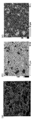
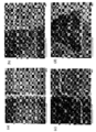
- (C) is a mapping image of Ni by EDX in the same field of view. It is a SEM image of the surface of a W-30 at% Ni target, (a) is a SEM image of the surface of the W-Ni sintered body (polished surface), and (b) is a WEM by EDX (energy dispersive X-ray spectroscopy) in the same field of view. (C) is a mapping image of Ni by EDX in the same field of view. In each of (a) W-10 at% Ni target, (b) W-20 at% Ni target, and (c) W-30 at% Ni target, the W-rich particle interface was observed and the line spectrum was taken. is there.
- (d) shows the result of taking a line spectrum with Ni-rich particles in W-20 at% Ni. It is a figure which shows the W peak (110) and NiW (042) peak by XRD measurement of a W-10at% Ni target (a), a W-20at% Ni target (b), and a W-30at% Ni target (c).
- the sputtering target for forming the barrier film of the present invention is composed of W powder having an average particle diameter of 1 to 5 ⁇ m and Ni powder having an average particle diameter of 1 to 30 ⁇ m, WxNiy (70 ⁇ x ⁇ 90, 10 ⁇ y ⁇ 30). ), And the mixture is sintered by hot pressing at a pressure of 10 to 50 MPa and 1300 to 1600 ° C.
- This sintering condition has a composition of WxNiy (70 ⁇ x ⁇ 90, 10 ⁇ y ⁇ 30), and the structure is composed of a W matrix and Ni particles existing therein, and W is diffused into the Ni particles.
- the W powder and the Ni powder may have an average particle size other than the above conditions. However, by using the powder having the above particle diameter, the target can be efficiently obtained.
- WxNiy 70 ⁇ x ⁇ 90, 10 ⁇ y ⁇ 30
- Ni and inevitable impurities are as follows. by. This is because when Ni exceeds 30 (y> 30), plasma is difficult to be generated during sputtering due to the magnetism of Ni, and efficient sputtering cannot be performed. Further, if y is less than 10, the plating property and the adhesiveness deteriorate, so 10 ⁇ y.
- the plating method is changed to the electroless plating method.
- a plating method such as an ion beam evaporation method or a sputtering method.
- the amount of Ni in W is preferably 20 to 30 (20 ⁇ y ⁇ 30).
- the electroless plating method has good plating properties. The most important thing is whether or not the material has a good barrier property.
- the barrier film for semiconductor wiring having the composition of WxNiy (70 ⁇ x ⁇ 90, 10 ⁇ y ⁇ 30) of the present invention effectively prevents copper from diffusing into the semiconductor element (silicon) or the insulating film, It has an excellent effect of eliminating factors that hinder the characteristics of semiconductors.
- the sintered body sputtering target of the present invention has several characteristics.
- the matrix of the sputtering target is W, and Ni particles of 2 to 40 ⁇ m are uniformly dispersed in the W matrix.
- W itself is crystallized at the time of sintering, but Ni particles of 2 to 5 ⁇ m exist at the triple point of the W crystal, and other excess Ni is uniformly in the W matrix as 20 to 40 ⁇ m particles.
- Ni particles are uniformly dispersed in the W matrix, but when viewed individually, they are dispersed in two forms: 2 to 5 ⁇ m Ni particles and Ni 20 to 40 ⁇ m particles. Yes.
- the number of Ni particles present varies depending on the amount of Ni contained, and in particular, the number of Ni 20 to 40 ⁇ m particles decreases as the Ni addition amount decreases.
- Ni particles present in the W matrix are preferably present as WNi particles. If Ni is present alone in the W matrix, it is not preferable because the magnetism of Ni hinders plasma generation during sputtering. In particular, when the sintering temperature is low and the sintering is not sufficient, the presence of Ni particles greatly affects the sputtering efficiency. Accordingly, it can be said that the Ni particles present in the W matrix are desirably present as non-magnetic WNi particles.
- the hot press temperature is preferably 1450 ° C. or lower, and is preferably 1400 ° C. or lower in consideration of safety.
- the purity is 4N5 or more, excluding gas components.
- W-Ni functions as a barrier film, and other impurities may contaminate the semiconductor film or the insulating film.
- contamination with impurities increases the possibility of deforming the target structure, and the above-mentioned suitable structure cannot be maintained, it is desirable to use a material having as high purity as possible.
- oxygen as gas components is 1000 wtppm or less and carbon is 50 ppm or less.
- oxygen as a gas component is more preferably 500 wtppm or less. This is because they cause the generation of particles in the same manner as described above.
- films with high oxygen and carbon have high film stress and are very easy to peel off. When these films adhere to the sputtering apparatus, sudden peeling of particles during the sputtering process occurs due to the peeling of the film. There is a problem of increasing.
- oxygen and carbon which are gas components, increase the possibility of forming oxides and carbides with constituent elements, and in the same way as described above, mixing of foreign substances such as oxides and carbides is a suitable target structure of the present invention. Can be said to be as small as possible.
- the amounts of the above impurities are not usually a major problem, and these are not a decisive factor as a function of the target, but they are reduced as much as possible for the above reasons. It goes without saying that it is preferable.
- the higher the relative density of the target the more the generation of particles can be suppressed, and it is 95.0% or more, preferably 99.0% or more, more preferably 99.9 or more. This increases the value as a target and is useful.
- the pressure of 10 to 50 MPa during sintering is naturally that the density does not increase at a low pressure of less than 10 MPa, but if a high pressure of more than 50 MPa is applied, a layered crack is generated parallel to the press surface. It is.
- Example 1 As the raw material powder, a powder having an average particle diameter of 5 ⁇ m as a W powder and a powder having an average particle diameter of 30 ⁇ m as a Ni powder were prepared so as to be W90Ni10 and mixed in a ball mill. Next, this mixed powder was filled in a carbon mold, heated to 1400 ° C. in a vacuum atmosphere, and hot pressed at 30 MPa. As a result, a sintered body having a relative density of 100% was obtained. Next, this was ground and polished to produce a target having a diameter of 330 mm and a thickness of 6.35 mm. Oxygen in the target was 120 wtppm and carbon was 30 wtppm. An SEM image of this target is shown in FIG.
- FIG. 1A is an SEM image of the surface (polished surface) of the W—Ni sintered body
- FIG. 1B is a mapping image of W by EDX (energy dispersive X-ray spectroscopy) in the same field
- FIG. 1C is the same field. It is a mapping image of Ni by EDX.
- the crystal structure of W can be observed.
- the middle figure (b) and the rightmost figure (c) it can be observed that fine Ni particles of 2 to 5 ⁇ m and large Ni particles of 20 to 40 ⁇ m are dispersed in the W structure.
- this target was set in a radio frequency (RF) sputtering apparatus.
- RF radio frequency
- single-crystal Si was set facing the substrate.
- RF sputtering was performed in an argon atmosphere.
- the applied voltage was RF 12 kW, and the film formation time was 50 seconds.
- a 15 nm barrier film was formed on the single crystal silicon substrate. At this time, the state of generation of particles was observed.
- a barrier film of 15 nm was formed on this silicon substrate, and copper was further formed to a thickness of 30 nm by electroless plating.
- the silicon substrate on which the copper layer was formed via the barrier film was subjected to 350 ° C. ⁇ temporary vacuum annealing treatment, and the state of copper diffusion was examined by AES depth profile measurement.
- Table 1 it was confirmed that the W90Ni10 thin film of Example 1 did not diffuse copper into the single crystal silicon substrate and had an excellent effect as a barrier layer.
- the electroless plating property and adhesion of copper are not good, but they are not a major obstacle.
- the generation of particles is extremely small and the barrier layer can be stably formed.
- Example 2 As the raw material powder, a powder having an average particle diameter of 5 ⁇ m as a W powder and a powder having an average particle diameter of 30 ⁇ m as a Ni powder were prepared so as to be W80Ni20 and mixed in a ball mill. Next, this mixed powder was filled in a carbon mold, heated to 1400 ° C. in a vacuum atmosphere, and hot pressed at 30 MPa. As a result, a sintered body having a relative density of 99.9% was obtained. Next, this was ground and polished to produce a target having a diameter of 330 mm and a thickness of 6.35 mm. Oxygen in the target was 100 wtppm and carbon was 30 wtppm. An SEM image of this target is shown in FIG.
- FIG. 2A is an SEM image of the surface (polished surface) of the W—Ni sintered body
- FIG. 2B is a mapping image of W by EDX (energy dispersive X-ray spectroscopy) in the same field
- FIG. 2C is the same field. It is a mapping image of Ni by EDX. From the center (b) and the right (c), it can be observed that fine Ni particles of 2 to 5 ⁇ m and large Ni particles of 20 to 40 ⁇ m are dispersed in W in the W structure. It can be seen that the number of large Ni particles of 20 to 40 ⁇ m shown in FIG. 2 of Example 2 is larger than the number of large Ni particles of 20 to 40 ⁇ m shown in FIG.
- this target was set in a radio frequency (RF) sputtering apparatus.
- RF radio frequency
- single-crystal Si was set facing the substrate.
- RF sputtering was performed in an argon atmosphere.
- the applied voltage was RF 12 kW, and the film formation time was 50 seconds.
- a 15 nm barrier film was formed on the single crystal silicon substrate. At this time, the state of generation of particles was observed.
- a barrier film of 15 nm was formed on this silicon substrate, and copper was further formed to a thickness of 30 nm by electroless plating.
- a silicon substrate on which a copper layer was formed via the barrier film was subjected to a vacuum annealing treatment at 350 ° C. for 1 hour, and the state of copper diffusion was examined by AES depth profile measurement.
- Table 1 it was confirmed that the W80Ni20 thin film of Example 2 did not diffuse copper into the single crystal silicon substrate and had an excellent effect as a barrier layer.
- the electroless plating property and adhesion of copper were both good.
- the generation of particles is extremely small and the barrier layer can be stably formed.
- Example 3 As raw powders, powders having an average particle diameter of 5 ⁇ m as W powders and powders having an average particle diameter of 30 ⁇ m as Ni powders were prepared so as to be W70Ni30 and mixed in a ball mill. Next, this mixed powder was filled in a carbon mold, heated to 1400 ° C. in a vacuum atmosphere, and hot pressed at 30 MPa. As a result, a sintered body having a relative density of 100% was obtained. Next, this was ground and polished to produce a target having a diameter of 330 mm and a thickness of 6.35 mm. The oxygen in the target was 130 wtppm and carbon was 20 wtppm.
- FIG. 3A is an SEM image of the surface (polished surface) of the W—Ni sintered body
- FIG. 3B is a mapping image of W by EDX (energy dispersive X-ray spectroscopy) in the same field
- FIG. 3C is the same field. It is a mapping image of Ni by EDX. From the center (b) and the right (c), it can be observed that fine Ni particles of 2 to 5 ⁇ m and large Ni particles of 20 to 40 ⁇ m are dispersed in W in the W structure. It can be seen that the number of large Ni particles of 20 to 40 ⁇ m shown in FIG. 3 of Example 3 is further increased than the number of large Ni particles of 20 to 40 ⁇ m shown in FIG.
- this target was set in a radio frequency (RF) sputtering apparatus.
- RF radio frequency
- single-crystal Si was set facing the substrate.
- RF sputtering was performed in an argon atmosphere.
- the applied voltage was RF 12 kW, and the film formation time was 50 seconds.
- a 15 nm barrier film was formed on the single crystal silicon substrate. At this time, the state of generation of particles was observed.
- a barrier film of 15 nm was formed on this silicon substrate, and copper was further formed to a thickness of 30 nm by electroless plating.
- a silicon substrate on which a copper layer was formed via the barrier film was subjected to a vacuum annealing treatment at 350 ° C. for 1 hour, and the state of copper diffusion was examined by AES depth profile measurement.
- Table 1 it was confirmed that the W70Ni30 thin film of Example 3 did not diffuse copper into the single crystal silicon substrate and had an excellent effect as a barrier layer.
- the electroless plating property and adhesion of copper were both good.
- the generation of particles is extremely small and the barrier layer can be stably formed.
- FIG. 4 The SEM images of the interface between W and Ni particles in Examples 1 to 3 are shown in FIG. In FIG. 4, (a) W-10 at% Ni target, (b) W-20 at% Ni target, and (c) W-30 at% Ni target, the interface of W-rich particles was observed, and the line spectrum was obtained. It was taken. In these, it is confirmed that Ni is hardly diffused in the W-rich particles, and that W is diffused in the Ni-rich particles.
- the lower right (d) of FIG. 4 shows the result of heat treatment at 1400 ° C. for 2 hours, and it can be confirmed that W is diffused in Ni.
- FIGS. Shown in (b) data confirming the presence of W and NiW by XRD measurement are shown in FIGS. Shown in (b).
- NiW (042) is the main peak of NiW, and the peak intensity increases as the amount of Ni added increases. From this, it can be seen that W diffuses in the Ni particles and an intermetallic compound of NiW is formed. Further, in FIG. 5, no Ni peak was confirmed, and it was confirmed that Ni was not present alone in the target.
- Example 4 As raw powders, powders having an average particle diameter of 1 ⁇ m as W powders and powders having an average particle diameter of 1 ⁇ m as Ni powders were prepared so as to be W90Ni10 and mixed in a ball mill. Next, this mixed powder was filled in a carbon mold, heated to 1400 ° C. in a vacuum atmosphere, and hot pressed at 30 MPa. As a result, a sintered body having a relative density of 96.1% was obtained. Next, this was ground and polished to produce a target having a diameter of 330 mm and a thickness of 6.35 mm. Oxygen in the target was 850 wtppm and carbon was 30 wtppm.
- Example 2 The amount of oxygen in this target increased compared to Example 1, which was thought to be due to the increased amount of oxygen adsorbed because the raw material powder used was fine. Although the SEM image of this target is omitted, similar to that shown in FIG. 1 of Example 1, fine Ni particles of 2 to 5 ⁇ m and large Ni particles of 20 to 40 ⁇ m are dispersed in W in the W structure. It was observed.
- this target was set in a radio frequency (RF) sputtering apparatus.
- RF radio frequency
- single-crystal Si was set facing the substrate.
- RF sputtering was performed in an argon atmosphere.
- the applied voltage was RF 12 kW, and the film formation time was 50 seconds.
- a 15 nm barrier film was formed on the single crystal silicon substrate. At this time, the state of generation of particles was observed.
- a barrier film of 15 nm was formed on this silicon substrate, and copper was further formed to a thickness of 30 nm by electroless plating.
- a silicon substrate on which a copper layer was formed via the barrier film was subjected to a vacuum annealing treatment at 350 ° C. for 1 hour, and the state of copper diffusion was examined by AES depth profile measurement.
- Table 1 it was confirmed that the W90Ni10 thin film of Example 4 did not diffuse copper into the single crystal silicon substrate and had an excellent effect as a barrier layer.
- the electroless plating property and adhesion of copper were slightly inferior.
- the generation of particles was not at a level that caused some problems. It was considered that the cause of the slight increase in the generation of particles due to the decrease in electroless plating and adhesion and the target density was somewhat low was the increase in the amount of oxygen. However, this level was not a problem.
- Example 5 As raw powders, powders having an average particle diameter of 1 ⁇ m as W powders and powders having an average particle diameter of 1 ⁇ m as Ni powders were prepared so as to be W80Ni20 and mixed in a ball mill. Next, this mixed powder was filled in a carbon mold, heated to 1400 ° C. in a vacuum atmosphere, and hot pressed at 30 MPa. As a result, a sintered body having a relative density of 96.5% was obtained. Next, this was ground and polished to produce a target having a diameter of 330 mm and a thickness of 6.35 mm. The oxygen in the target was 730 wtppm and carbon was 40 wtppm.
- the amount of oxygen in this target increased as compared with Example 2, which was thought to be due to an increase in the amount of oxygen adsorbed because the raw material powder used was fine.
- fine Ni particles of 2 to 5 ⁇ m and large Ni particles of 20 to 40 ⁇ m are dispersed in W in the W structure, similar to that shown in FIG. It was observed.
- this target was set in a radio frequency (RF) sputtering apparatus.
- RF radio frequency
- single-crystal Si was set facing the substrate.
- RF sputtering was performed in an argon atmosphere.
- the applied voltage was RF 12 kW, and the film formation time was 50 seconds.
- a 15 nm barrier film was formed on the single crystal silicon substrate. At this time, the state of generation of particles was observed.
- a barrier film of 15 nm was formed on this silicon substrate, and copper was further formed to a thickness of 30 nm by electroless plating.
- a silicon substrate on which a copper layer was formed via the barrier film was subjected to a vacuum annealing treatment at 350 ° C. for 1 hour, and the state of copper diffusion was examined by AES depth profile measurement.
- Table 1 it was confirmed that the W80Ni20 thin film of Example 5 did not diffuse copper into the single crystal silicon substrate and had an excellent effect as a barrier layer.
- production of the particle was recognized, but it was not the level which becomes a problem in particular. The cause of the slight increase in particle generation was thought to be an increase in the amount of oxygen. However, this level was not a problem.
- Example 6 As the raw material powder, powder having an average particle diameter of 1 ⁇ m as W powder and powder having an average particle diameter of 1 ⁇ m as Ni powder were prepared so as to be W70Ni30 and mixed in a ball mill. Next, this mixed powder was filled in a carbon mold, heated to 1400 ° C. in a vacuum atmosphere, and hot pressed at 30 MPa. As a result, a sintered body having a relative density of 97.3% was obtained. Next, this was ground and polished to produce a target having a diameter of 330 mm and a thickness of 6.35 mm. The oxygen in the target was 730 wtppm and carbon was 40 wtppm.
- Example 3 The amount of oxygen in this target increased as compared with Example 3, which was thought to be due to the increased amount of oxygen adsorbed because the raw material powder used was fine. Although the SEM image of this target is omitted, similar to the one shown in FIG. 3 of Example 3, fine Ni particles of 2 to 5 ⁇ m and large Ni particles of 20 to 40 ⁇ m are dispersed in W in the W tissue. It was observed.
- this target was set in a radio frequency (RF) sputtering apparatus.
- RF radio frequency
- single-crystal Si was set facing the substrate.
- RF sputtering was performed in an argon atmosphere.
- the applied voltage was RF 12 kW, and the film formation time was 50 seconds.
- a 15 nm barrier film was formed on the single crystal silicon substrate. At this time, the state of generation of particles was observed.
- a barrier film of 15 nm was formed on this silicon substrate, and copper was further formed to a thickness of 30 nm by electroless plating.
- a silicon substrate on which a copper layer was formed via the barrier film was subjected to a vacuum annealing treatment at 350 ° C. for 1 hour, and the state of copper diffusion was examined by AES depth profile measurement.
- Table 1 it was confirmed that the W70Ni30 thin film of Example 5 did not diffuse copper into the single crystal silicon substrate and had an excellent effect as a barrier layer.
- production of the particle was recognized, but it was not the level which becomes a problem in particular. The cause of the slight increase in particle generation was thought to be an increase in the amount of oxygen. However, this level was not a problem.
- a powder having an average particle diameter of 5 ⁇ m as a W powder and a powder having an average particle diameter of 30 ⁇ m as a Ni powder were prepared so as to be W80Ni20 and mixed in a ball mill.
- this mixed powder was filled in a carbon mold, heated to 1200 ° C. in a vacuum atmosphere, and hot pressed at 30 MPa.
- a sintered body having a relative density of 87.1% was obtained.
- this was ground and polished to produce a target having a diameter of 330 mm and a thickness of 6.35 mm.
- Oxygen in the target was 900 wtppm and carbon was 20 wtppm.
- a powder having an average particle diameter of 5 ⁇ m as a W powder and a powder having an average particle diameter of 30 ⁇ m as a Ni powder were prepared so as to be W80Ni20 and mixed in a ball mill.
- this mixed powder was filled in a carbon mold, heated to 1000 ° C. in a vacuum atmosphere, and hot pressed at 30 MPa.
- a sintered body having a relative density of 86.2% was obtained.
- this was ground and polished to produce a target having a diameter of 330 mm and a thickness of 6.35 mm.
- Oxygen in the target was 840 wtppm and carbon was 30 wtppm.
- this target was set in a radio frequency (RF) sputtering apparatus.
- RF radio frequency
- single-crystal Si was set facing the substrate.
- RF sputtering was performed in an argon atmosphere.
- the applied voltage was RF 12 kW, and the film formation time was 50 seconds.
- no plasma was generated and the sputtering property was poor. This is probably because the hot press temperature is low, so that W does not sufficiently diffuse into the target Ni particles and exists as pure Ni particles, and the plasma does not form during sputtering due to the magnetism of the Ni particles.
- Comparative Example 4 As the raw material powder, powder having an average particle diameter of 1 ⁇ m as W powder and powder having an average particle diameter of 1 ⁇ m as Ni powder were prepared so as to be W70Ni30 and mixed in a ball mill. Next, this mixed powder was filled in a carbon mold, heated to 1000 ° C. in a vacuum atmosphere, and hot pressed at 30 MPa. As a result, a sintered body having a relative density of 85.8% was obtained. Next, this was ground and polished to produce a target having a diameter of 330 mm and a thickness of 6.35 mm. Oxygen in the target was 1200 wtppm and carbon was 30 wtppm. Since the raw material powder was fine, the amount of oxygen further increased.
- this target was set in a radio frequency (RF) sputtering apparatus.
- RF radio frequency
- single-crystal Si was set facing the substrate.
- RF sputtering was performed in an argon atmosphere.
- the applied voltage was RF 12 kW, and the film formation time was 50 seconds.
- no plasma was generated and the sputtering property was poor. This is probably because the hot press temperature is low, so that W does not sufficiently diffuse into the target Ni particles and exists as pure Ni particles, and the plasma does not form during sputtering due to the magnetism of the Ni particles.
- the sintered sputtering target for forming the barrier film for semiconductor wiring of the present invention contains Ni, and the balance is made of W and inevitable impurities.
- having a composition of WxNiy (70 ⁇ x ⁇ 90, 10 ⁇ y ⁇ 30) is indispensable as a barrier film for semiconductor wiring, but the target structure is composed of a W matrix and Ni particles present therein.
- the Ni particles have a structure in which W is diffused.
- This target has a good sputtering property, generates few particles, and has a material as a good target.
- a film having a composition of WxNiy (70 ⁇ x ⁇ 90, 10 ⁇ y ⁇ 30) can be formed, which is remarkably excellent as a barrier film for semiconductor wiring, It also has excellent plating properties and plating adhesion.
- the present invention can effectively prevent a reaction between layers in a semiconductor device without depending on a nitriding reaction at the time of sputtering, and further, a sputtering target suitable for a barrier film that does not generate particles at the time of sputtering. Since it has the outstanding effect that a manufacturing method and the same barrier film can be obtained, it is useful as a constituent material of a semiconductor device.
Landscapes
- Chemical & Material Sciences (AREA)
- Engineering & Computer Science (AREA)
- Materials Engineering (AREA)
- Mechanical Engineering (AREA)
- Metallurgy (AREA)
- Organic Chemistry (AREA)
- Chemical Kinetics & Catalysis (AREA)
- Physics & Mathematics (AREA)
- Plasma & Fusion (AREA)
- Analytical Chemistry (AREA)
- Physical Vapour Deposition (AREA)
- Electrodes Of Semiconductors (AREA)
Abstract
Description
例えば、銅配線を形成する溝の凹部に高純度タンタルターゲットでスパッタリングによりタンタル若しくは窒化タンタルを成膜して拡散バリア膜を形成し、次いで銅あるいは銅合金からなるシード層をスパッタリングにより成膜し、最後に電気めっきで銅を埋め込むことにより行われている。
この場合、予めタンタルシリサイドを主成分とするターゲットを作製し、これを窒素雰囲気中で反応性スパッタリングを行い窒化して、タンタルシリコンナイトライドのバリア膜を形成するというものであるが、スパッタリング中の窒化反応を期待するものであるために、形成された窒化膜の性質にバラツキが生ずるという問題がある。
また、このようなバラツキを減少させるためには、ターゲットの組成比を厳密な調整、窒素とアルゴン等のスパッタガスとの比率の調整及びスパッタ装置内への一定量の導入、基板温度調節等の、スパッタリング条件を厳密に調整しなければならない煩雑さが生ずる。
半導体素子の配線幅は高密度化に従って、更に狭くなる方向に向かっており、よりバリア性が高く、かつ低抵抗なTa-Si-Bのような3元系のバリア膜も検討されている。この場合、低抵抗化のために金属成分のタンタルが多く、高温安定性を改善するために、ボロンを少し添加することが良いと考えられるが、タンタル粉、シリコン粉とボロン粉の混合粉をホットプレスやHIPで焼結しても、密度を十分に向上することはできず、スパッタリングターゲットとして使用できるものはなかった。
また、タングステンにニッケルを添加した製造方法の特許文献がある(特許文献2、3、4参照)。これらは、使用目的が異なるために、バリア膜としての機能及びそれを作製するための方法を開示するものではないが、参考までに掲げる。
1)Niを含有し、残余がW及び不可避的不純物からなり、WxNiy(70≦x≦90、10≦y≦30)の組成を有する半導体配線用バリア膜。なお、x+y=100%である(単位:at%、以下同様である)。
3)スパッタリングターゲットがWマトリックスを備え、該Wマトリックス中に2~40μmのNi粒子が分散していることを特徴とする上記2)記載の焼結体スパッタリングターゲット。
4)Wマトリックス中に2~5μmのNi粒子と20~40μmのNi粒子とが分散していることを特徴とする上記3)記載の焼結体スパッタリングターゲット。
5)Wマトリックス中に存在するNi粒子はWNi粒子であることを特徴とする上記3)又は4)記載の焼結体スパッタリングターゲット。
6)ガス成分を除き、純度が4N5以上を備えていることを特徴とする上記2)~5)のいずれか一項に記載の焼結体スパッタリングターゲット。
7)ガス成分である酸素が1000wtppm以下、炭素が50ppm以下であることを特徴とする上記6)記載の焼結体スパッタリングターゲット。
8)ガス成分である酸素が500wtppm以下であることを特徴とする上記7)記載の焼結体スパッタリングターゲット。
9)相対密度が95.0%以上であることを特徴とする上記2)~8)のいずれか一項に記載の焼結体スパッタリングターゲット。
この焼結条件は、WxNiy(70≦x≦90、10≦y≦30)の組成を有すると共に、組織がWマトリックスとその中に存在するNi粒子からなり、該Ni粒子にWが拡散した組織を備えている焼結体スパッタリングターゲットを得るための条件であり、このターゲットを得ることができれば、この製造方法に特に限定されるものではない。例えばW粉末及びNi粉末は、上記条件以外の平均粒径を有していても良い。しかし、上記粒径の粉末を用いることにより、効率的に目的とするターゲットを得ることができる。
Niが30を超える(y>30)場合には、Niの磁性によりスパッタリング時にプラズマが立ち難く、効率的なスパッタリングができないためである。また、yが10未満ではめっき性及び密着性が悪くなるので、10≦yとする。
最も重要なことは良好なバリア性を備える材料であるか否かである。本発明のWxNiy(70≦x≦90、10≦y≦30)の組成を有する半導体配線用バリア膜は、銅が半導体素子(シリコン)又は絶縁膜中に拡散するのを効果的に防止し、半導体の特性を阻害する要因を排除できる優れた効果を有する。
W自体は焼結時に結晶化されているが、このW結晶の三重点に2~5μmのNi粒子が存在し、これ以外の過剰部分のNiは20~40μmの粒子としてWマトリックスの中に均一に分散している。したがって、トータルでみるとWマトリックス中に2~40μmのNi粒子が均一に分散しているが、個々にみると2~5μmのNi粒子とNi20~40μmの粒子の2種類の形態で分散している。
また、このNi粒子の存在の個数は、含有するNi量によって変化し、特にNi20~40μmの粒子の個数は、Ni添加量が少なくなるにしたがって減少する。
特に焼結温度が低く焼結が十分でない場合には、Ni粒子として存在するために、スパッタリングの効率に大きく影響する。したがって、Wマトリックス中に存在するNi粒子は、非磁性のWNi粒子として存在することが望ましいと言える。
また、ガス成分である酸素及び炭素は、構成元素との酸化物及び炭化物を形成する可能性が高くなり、上記と同様に、酸化物、炭化物等の異物の混入は本願発明の好適なターゲット組織を変形又は部分的に破壊するので、できるだけ少ない方が望ましいと言える。
また、ターゲットの相対密度は高い方が、パーティクル発生を抑制することができ、95.0%以上、好ましくは99.0%以上、より好ましくは99.9以上である。これはターゲットとしての価値を高め、有用である。
焼結時に10~50MPaの加圧力とするのは、10MPa未満の低圧では密度向上しないことは当然であるが、50MPaを超える高圧をかけると、プレス面に平行に層状クラックが発生してしまうためである。
原料粉末として、W粉末として平均粒径5μm、Ni粉末として平均粒径30μmの粉末を用い、これらがW90Ni10となるように調合し、ボールミル中で混合した。
次に、この混合粉末を、カーボンモールド中に充填し、真空雰囲気中で、1400°Cに加熱し、30MPaでホットプレスした。
この結果、相対密度100%の焼結体が得られた。次に、これを研削及び研磨加工して、直径330mm、厚さ6.35mmのターゲットを作製した。ターゲット中の酸素は120wtppm、炭素30wtppmであった。
このターゲットのSEM画像を図1に示す。図1の(a)はW-Ni焼結体表面(研磨面)のSEM像、(b)は同視野におけるEDX(エネルギー分散X線分光法)によるWのマッピング像、(c)は同視野におけるEDXによるNiのマッピング像である。
最左の図(a)はWの結晶組織が観察できる。中央の図(b)と最右の図(c)から、W組織の中に2~5μmの細かいNi粒子と20~40μmの大きなNi粒子がW中に分散しているのが観察できる。
この条件で、アルゴン雰囲気中でRFスパッタリングを実施した。印加電圧はRF12kW、成膜時間は50秒とした。
これによって、15nmのバリア膜が単結晶シリコン基板上に形成された。この時の、パーティクルの発生状況を観察した。
この結果を、表1にまとめた。この表1に示すように、実施例1のW90Ni10薄膜は、単結晶シリコン基板への銅の拡散が認められず、バリア層として優れた効果を有することが確認できた。一方、銅の無電解めっき性及び密着性は、良いというものではないが、大きな障害となるものではなかった。そして、また、パーティクルの発生は極めて少なく、バリア層の安定した成膜が可能であるという、特徴も備えていた。

原料粉末として、W粉末として平均粒径5μm、Ni粉末として平均粒径30μmの粉末を用い、これらがW80Ni20となるように調合し、ボールミル中で混合した。
次に、この混合粉末を、カーボンモールド中に充填し、真空雰囲気中で、1400°Cに加熱し、30MPaでホットプレスした。
この結果、相対密度99.9%の焼結体が得られた。次に、これを研削及び研磨加工して、直径330mm、厚さ6.35mmのターゲットを作製した。ターゲット中の酸素は100wtppm、炭素30wtppmであった。
このターゲットのSEM画像を図2に示す。図2の(a)はW-Ni焼結体表面(研磨面)のSEM像、(b)は同視野におけるEDX(エネルギー分散X線分光法)によるWのマッピング像、(c)は同視野におけるEDXによるNiのマッピング像である。
中央の図(b)と右の図(c)から、W組織の中に2~5μmの細かいNi粒子と20~40μmの大きなNi粒子がW中に分散しているのが観察できる。
本実施例2の図2に示す20~40μmの大きなNi粒子の個数は、前記実施例1の図1に示す20~40μmの大きなNi粒子の個数よりも増加しているのが分かる。
この条件で、アルゴン雰囲気中でRFスパッタリングを実施した。印加電圧はRF12kW、成膜時間は50秒とした。
これによって、15nmのバリア膜が単結晶シリコン基板上に形成された。この時の、パーティクルの発生状況を観察した。
この結果を、表1にまとめた。この表1に示すように、実施例2のW80Ni20薄膜は、単結晶シリコン基板への銅の拡散が認められず、バリア層として優れた効果を有することが確認できた。一方、銅の無電解めっき性及び密着性は、いずれも良好であった。そして、また、パーティクルの発生は極めて少なく、バリア層の安定した成膜が可能であるという、特徴も備えていた。
原料粉末として、W粉末として平均粒径5μm、Ni粉末として平均粒径30μmの粉末を用い、これらがW70Ni30となるように調合し、ボールミル中で混合した。
次に、この混合粉末を、カーボンモールド中に充填し、真空雰囲気中で、1400°Cに加熱し、30MPaでホットプレスした。
この結果、相対密度100%の焼結体が得られた。次に、これを研削及び研磨加工して、直径330mm、厚さ6.35mmのターゲットを作製した。ターゲット中の酸素は130wtppm、炭素20wtppmであった。
中央の図(b)と右の図(c)から、W組織の中に2~5μmの細かいNi粒子と20~40μmの大きなNi粒子がW中に分散しているのが観察できる。
本実施例3の図3に示す20~40μmの大きなNi粒子の個数は、前記実施例2の図2に示す20~40μmの大きなNi粒子の個数よりも、さらに増加しているのが分かる。
この条件で、アルゴン雰囲気中でRFスパッタリングを実施した。印加電圧はRF12kW、成膜時間は50秒とした。
これによって、15nmのバリア膜が単結晶シリコン基板上に形成された。この時の、パーティクルの発生状況を観察した。
この結果を、表1にまとめた。この表1に示すように、実施例3のW70Ni30薄膜は、単結晶シリコン基板への銅の拡散が認められず、バリア層として優れた効果を有することが確認できた。一方、銅の無電解めっき性及び密着性は、いずれも良好であった。そして、また、パーティクルの発生は極めて少なく、バリア層の安定した成膜が可能であるという、特徴も備えていた。
図4の右下の(d)は、1400°C、2時間の加熱処理をした結果であり、Ni中にWが拡散していることが確認できる。
この図5(a)~(b)において、NiWの(042)は、NiWのメインピークであり、Niの添加量の増加と共に、ピーク強度も高くなっている。このことから、Ni粒子にはWが拡散し、NiWの金属間化合物が形成されていることが分かる。また、この図5ではNiのピークは確認されず、ターゲット中にNiが単独で存在することがないことが確認できた。
原料粉末として、W粉末として平均粒径1μm、Ni粉末として平均粒径1μmの粉末を用い、これらがW90Ni10となるように調合し、ボールミル中で混合した。
次に、この混合粉末を、カーボンモールド中に充填し、真空雰囲気中で、1400°Cに加熱し、30MPaでホットプレスした。
この結果、相対密度96.1%の焼結体が得られた。次に、これを研削及び研磨加工して、直径330mm、厚さ6.35mmのターゲットを作製した。ターゲット中の酸素は850wtppm、炭素30wtppmであった。このターゲットの酸素量は実施例1に比べて増加したが、これは使用した原料粉末が微細であるために、酸素の吸着量が増加したと考えられた。
このターゲットのSEM画像については省略するが、実施例1の図1に示すものと同様に、W組織の中に2~5μmの細かいNi粒子と20~40μmの大きなNi粒子がW中に分散しているのが観察された。
この条件で、アルゴン雰囲気中でRFスパッタリングを実施した。印加電圧はRF12kW、成膜時間は50秒とした。これによって、15nmのバリア膜が単結晶シリコン基板上に形成された。この時の、パーティクルの発生状況を観察した。
この結果を、表1にまとめた。この表1に示すように、実施例4のW90Ni10薄膜は、単結晶シリコン基板への銅の拡散が認められず、バリア層として優れた効果を有することが確認できた。一方、銅の無電解めっき性及び密着性は、やや劣る結果となった。そして、パーティクルの発生も、ややあるが問題となるレベルではなかった。
無電解めっき性及び密着性の低下並びにターゲットの密度がやや低いためにパーティクルの発生がやや増加した原因は、酸素量の増加にあることが考えられた。しかし、このレベルでは特に問題となるものではなかった。
原料粉末として、W粉末として平均粒径1μm、Ni粉末として平均粒径1μmの粉末を用い、これらがW80Ni20となるように調合し、ボールミル中で混合した。
次に、この混合粉末を、カーボンモールド中に充填し、真空雰囲気中で、1400°Cに加熱し、30MPaでホットプレスした。
この結果、相対密度96.5%の焼結体が得られた。次に、これを研削及び研磨加工して、直径330mm、厚さ6.35mmのターゲットを作製した。ターゲット中の酸素は730wtppm、炭素40wtppmであった。このターゲットの酸素量は実施例2に比べて増加したが、これは使用した原料粉末が微細であるために、酸素の吸着量が増加したと考えられた。
このターゲットのSEM画像については省略するが、実施例2の図2に示すものと同様に、W組織の中に2~5μmの細かいNi粒子と20~40μmの大きなNi粒子がW中に分散しているのが観察された。
この条件で、アルゴン雰囲気中でRFスパッタリングを実施した。印加電圧はRF12kW、成膜時間は50秒とした。これによって、15nmのバリア膜が単結晶シリコン基板上に形成された。この時の、パーティクルの発生状況を観察した。
この結果を、表1にまとめた。この表1に示すように、実施例5のW80Ni20薄膜は、単結晶シリコン基板への銅の拡散が認められず、バリア層として優れた効果を有することが確認できた。一方、銅の無電解めっき性及び密着性も良好であった。そして、パーティクルの発生が認められたが、特に問題となるレベルではなかった。
パーティクルの発生がやや増加した原因は、酸素量の増加にあることが考えられた。しかし、このレベルでは特に問題となるものではなかった。
原料粉末として、W粉末として平均粒径1μm、Ni粉末として平均粒径1μmの粉末を用い、これらがW70Ni30となるように調合し、ボールミル中で混合した。
次に、この混合粉末を、カーボンモールド中に充填し、真空雰囲気中で、1400°Cに加熱し、30MPaでホットプレスした。
この結果、相対密度97.3%の焼結体が得られた。次に、これを研削及び研磨加工して、直径330mm、厚さ6.35mmのターゲットを作製した。ターゲット中の酸素は730wtppm、炭素40wtppmであった。このターゲットの酸素量は実施例3に比べて増加したが、これは使用した原料粉末が微細であるために、酸素の吸着量が増加したと考えられた。
このターゲットのSEM画像については省略するが、実施例3の図3に示すものと同様に、W組織の中に2~5μmの細かいNi粒子と20~40μmの大きなNi粒子がW中に分散しているのが観察された。
この条件で、アルゴン雰囲気中でRFスパッタリングを実施した。印加電圧はRF12kW、成膜時間は50秒とした。これによって、15nmのバリア膜が単結晶シリコン基板上に形成された。この時の、パーティクルの発生状況を観察した。
この結果を、表1にまとめた。この表1に示すように、実施例5のW70Ni30薄膜は、単結晶シリコン基板への銅の拡散が認められず、バリア層として優れた効果を有することが確認できた。一方、銅の無電解めっき性及び密着性も良好であった。そして、パーティクルの発生が認められたが、特に問題となるレベルではなかった。
パーティクルの発生がやや増加した原因は、酸素量の増加にあることが考えられた。しかし、このレベルでは特に問題となるものではなかった。
原料粉末として、W粉末として平均粒径5μm、Ni粉末として平均粒径30μmの粉末を用い、これらがW80Ni20となるように調合し、ボールミル中で混合した。
次に、この混合粉末を、カーボンモールド中に充填し、真空雰囲気中で、1200°Cに加熱し、30MPaでホットプレスした。
この結果、相対密度87.1%の焼結体が得られた。次に、これを研削及び研磨加工して、直径330mm、厚さ6.35mmのターゲットを作製した。ターゲット中の酸素は900wtppm、炭素20wtppmであった。
この条件で、アルゴン雰囲気中でRFスパッタリングを実施した。印加電圧はRF12kW、成膜時間は50秒とした。しかし、プラズマが立たず、スパッタ性が悪かった。この原因は、ホットプレス温度が低いために、ターゲットのNi粒子中にWが十分に拡散せず、純Ni粒子として存在し、このNi粒子の磁性によりスパッタリング時にプラズマが立たなかったと考えられる。
また、強引にスパッタリングを実施したが、密度が低いためにパーティクルが大量に発生した。この状況から均一な成膜が難しいことが分かった。
このような状況から、バリア性、めっき性、めっき膜の密着性を確認する意味がないので、その後の調査はしなかった。この結果を表1に示す。
原料粉末として、W粉末として平均粒径5μm、Ni粉末として平均粒径30μmの粉末を用い、これらがW80Ni20となるように調合し、ボールミル中で混合した。
次に、この混合粉末を、カーボンモールド中に充填し、真空雰囲気中で、1000°Cに加熱し、30MPaでホットプレスした。
この結果、相対密度86.2%の焼結体が得られた。次に、これを研削及び研磨加工して、直径330mm、厚さ6.35mmのターゲットを作製した。ターゲット中の酸素は840wtppm、炭素30wtppmであった。
この条件で、アルゴン雰囲気中でRFスパッタリングを実施した。印加電圧はRF12kW、成膜時間は50秒とした。しかし、比較例1と同様にプラズマが立たず、スパッタ性が悪かった。この原因は、ホットプレス温度が低いために、ターゲットのNi粒子中にWが十分に拡散せず、純Ni粒子として存在し、このNi粒子の磁性によりスパッタリング時にプラズマが立たなかったと考えられる。
また、強引にスパッタリングを実施したが、密度が低いためにパーティクルが大量に発生した。この状況から均一な成膜が難しいことが分かった。
このような状況から、バリア性、めっき性、めっき膜の密着性を確認する意味がないので、その後の調査はしなかった。この結果を表1に示す。
原料粉末として、W粉末として平均粒径1μm、Ni粉末として平均粒径1μmの粉末を用い、これらがW80Ni20となるように調合し、ボールミル中で混合した。
次に、この混合粉末を、カーボンモールド中に充填し、真空雰囲気中で、1200°Cに加熱し、30MPaでホットプレスした。
この結果、相対密度83.4%の焼結体が得られた。次に、これを研削及び研磨加工して、直径330mm、厚さ6.35mmのターゲットを作製した。ターゲット中の酸素は1340wtppm、炭素40wtppmであった。原料粉末が微細なために、さらに酸素量が増加した。
この条件で、アルゴン雰囲気中でRFスパッタリングを実施した。印加電圧はRF12kW、成膜時間は50秒とした。しかし、比較例1と同様にプラズマが立たず、スパッタ性が悪かった。この原因は、ホットプレス温度が低いために、ターゲットのNi粒子中にWが十分に拡散せず、純Ni粒子として存在し、このNi粒子の磁性によりスパッタリング時にプラズマが立たなかったと考えられる。
また、強引にスパッタリングを実施したが、密度が低いためにパーティクルが大量に発生した。この状況から均一な成膜が難しいことが分かった。
このような状況から、バリア性、めっき性、めっき膜の密着性を確認する意味がないので、その後の調査はしなかった。この結果を表1に示す。
原料粉末として、W粉末として平均粒径1μm、Ni粉末として平均粒径1μmの粉末を用い、これらがW70Ni30となるように調合し、ボールミル中で混合した。
次に、この混合粉末を、カーボンモールド中に充填し、真空雰囲気中で、1000°Cに加熱し、30MPaでホットプレスした。
この結果、相対密度85.8%の焼結体が得られた。次に、これを研削及び研磨加工して、直径330mm、厚さ6.35mmのターゲットを作製した。ターゲット中の酸素は1200wtppm、炭素30wtppmであった。原料粉末が微細なために、さらに酸素量が増加した。
この条件で、アルゴン雰囲気中でRFスパッタリングを実施した。印加電圧はRF12kW、成膜時間は50秒とした。しかし、比較例1と同様にプラズマが立たず、スパッタ性が悪かった。この原因は、ホットプレス温度が低いために、ターゲットのNi粒子中にWが十分に拡散せず、純Ni粒子として存在し、このNi粒子の磁性によりスパッタリング時にプラズマが立たなかったと考えられる。
また、強引にスパッタリングを実施したが、密度が低いためにパーティクルが大量に発生した。この状況から均一な成膜が難しいことが分かった。
このような状況から、バリア性、めっき性、めっき膜の密着性を確認する意味がないので、その後の調査はしなかった。この結果を表1に示す。
このターゲットはスパッタリング性が良好であり、かつパーティクル発生が少なく、良好なターゲットとしての材質を備えている。
そして、このターゲットを使用してスパッタリングすることにより、WxNiy(70≦x≦90、10≦y≦30)の組成を有する膜を形成できるが、これは半導体配線用バリア膜として著しく優れており、まためっき性、めっき密着性にも優れている。
Claims (10)
- Niを含有し、残余がW及び不可避的不純物からなり、WxNiy(70≦x≦90、10≦y≦30、単位:at%)の組成を有する半導体配線用バリア膜。
- Niを含有し、残余がW及び不可避的不純物からなるターゲットであって、WxNiy(70≦x≦90、10≦y≦30、単位:at%)の組成を有すると共に、ターゲットの組織はWマトリックスとその中に存在するNi粒子からなり、該Ni粒子にWが拡散した組織を備えていることを特徴とする半導体配線用バリア膜を形成するための焼結体スパッタリングターゲット。
- スパッタリングターゲットがWマトリックスを備え、該Wマトリックス中に2~40μmのNi粒子が分散していることを特徴とする請求項2記載の焼結体スパッタリングターゲット。
- Wマトリックス中に2~5μmのNi粒子と20~40μmのNi粒子とが分散していることを特徴とする請求項3記載の焼結体スパッタリングターゲット。
- Wマトリックス中に存在するNi粒子はWNi粒子であることを特徴とする請求項3又は4記載の焼結体スパッタリングターゲット。
- ガス成分を除き、純度が4N5以上を備えていることを特徴とする請求項2~5のいずれか一項に記載の焼結体スパッタリングターゲット。
- ガス成分である酸素が1000wtppm以下、炭素が50ppm以下であることを特徴とする請求項6記載の焼結体スパッタリングターゲット。
- ガス成分である酸素が500wtppm以下であることを特徴とする請求項7記載の焼結体スパッタリングターゲット。
- 相対密度が95.0%以上であることを特徴とする請求項2~8のいずれか一項に記載の焼結体スパッタリングターゲット。
- 平均粒径が1~5μmのW粉末と平均粒径が1~30μmのNi粉末を、WxNiy(70≦x≦90、10≦y≦30、単位:at%)の配合比となるように混合し、これを10~50MPaの加圧力、1300~1600°Cでホットプレスにより焼結することを特徴とするスパッタリングターゲットの製造方法。
Priority Applications (5)
| Application Number | Priority Date | Filing Date | Title |
|---|---|---|---|
| US13/059,582 US9051645B2 (en) | 2009-04-17 | 2010-04-05 | Barrier film for semiconductor wiring, sintered compact sputtering target and method of producing the sputtering target |
| JP2010531181A JP4647724B2 (ja) | 2009-04-17 | 2010-04-05 | 半導体配線用バリア膜、焼結体スパッタリングターゲット及びスパッタリングターゲットの製造方法 |
| SG2011044955A SG172268A1 (en) | 2009-04-17 | 2010-04-05 | Barrier film for semiconductor wiring, sintered compact sputtering target and method of producing the sputtering target |
| EP10764370.2A EP2431494B1 (en) | 2009-04-17 | 2010-04-05 | Barrier film for semiconductor wiring, sintered sputtering target, and method of manufacturing sputtering targets |
| CN201080003041.6A CN102197155B (zh) | 2009-04-17 | 2010-04-05 | 半导体布线用阻挡膜、烧结体溅射靶及溅射靶的制造方法 |
Applications Claiming Priority (2)
| Application Number | Priority Date | Filing Date | Title |
|---|---|---|---|
| JP2009-100666 | 2009-04-17 | ||
| JP2009100666 | 2009-04-17 |
Publications (1)
| Publication Number | Publication Date |
|---|---|
| WO2010119785A1 true WO2010119785A1 (ja) | 2010-10-21 |
Family
ID=42982447
Family Applications (1)
| Application Number | Title | Priority Date | Filing Date |
|---|---|---|---|
| PCT/JP2010/056152 Ceased WO2010119785A1 (ja) | 2009-04-17 | 2010-04-05 | 半導体配線用バリア膜、焼結体スパッタリングターゲット及びスパッタリングターゲットの製造方法 |
Country Status (8)
| Country | Link |
|---|---|
| US (1) | US9051645B2 (ja) |
| EP (1) | EP2431494B1 (ja) |
| JP (1) | JP4647724B2 (ja) |
| KR (1) | KR101078630B1 (ja) |
| CN (1) | CN102197155B (ja) |
| SG (1) | SG172268A1 (ja) |
| TW (1) | TWI354351B (ja) |
| WO (1) | WO2010119785A1 (ja) |
Cited By (3)
| Publication number | Priority date | Publication date | Assignee | Title |
|---|---|---|---|---|
| JP2015193909A (ja) * | 2014-03-25 | 2015-11-05 | Jx日鉱日石金属株式会社 | スパッタリングターゲット及びその製造方法並びにスパッタリング法で形成した膜 |
| KR20170046723A (ko) | 2014-09-30 | 2017-05-02 | 제이엑스금속주식회사 | 텅스텐 스퍼터링 타깃 및 그 제조 방법 |
| US11746409B2 (en) | 2013-12-20 | 2023-09-05 | Plansee Se | Process for producing and using a W—Ni sputtering target |
Families Citing this family (3)
| Publication number | Priority date | Publication date | Assignee | Title |
|---|---|---|---|---|
| KR101923551B1 (ko) | 2011-06-22 | 2018-11-30 | 삼성전자주식회사 | 무선 통신 시스템에서 망 진입을 위한 장치 및 방법 |
| WO2021054136A1 (ja) * | 2019-09-19 | 2021-03-25 | 日立金属株式会社 | ターゲット |
| CN116334563A (zh) * | 2023-04-19 | 2023-06-27 | 攀时(上海)高性能材料有限公司 | 溅射靶及制造溅射靶的方法 |
Citations (8)
| Publication number | Priority date | Publication date | Assignee | Title |
|---|---|---|---|---|
| JPS58144401A (ja) | 1982-02-22 | 1983-08-27 | Toshiba Corp | タングステン合金の製造方法 |
| JPH02163337A (ja) | 1988-12-16 | 1990-06-22 | Nippon Yakin Kogyo Co Ltd | 高硬度タングステン液相焼結合金の製造方法 |
| JPH11200025A (ja) | 1998-01-08 | 1999-07-27 | Mitsubishi Materials Corp | タンタルシリコンナイトライド薄膜形成用スパッタリングターゲット材 |
| JP2000169923A (ja) * | 1998-12-04 | 2000-06-20 | Sumitomo Metal Mining Co Ltd | W−Ni系ターゲット材料、電極材料、及び実装部品 |
| JP2000306863A (ja) * | 1991-01-25 | 2000-11-02 | Toshiba Corp | スパッタリングターゲット |
| JP2003031576A (ja) * | 2001-07-17 | 2003-01-31 | Nec Corp | 半導体素子及びその製造方法 |
| JP2003049264A (ja) * | 2000-09-07 | 2003-02-21 | Toshiba Corp | タングステンスパッタリングターゲットおよびその製造方法 |
| JP2003064440A (ja) | 2001-08-20 | 2003-03-05 | Mitsubishi Material Cmi Kk | 高比重高強度タングステン焼結合金製ウェート |
Family Cites Families (15)
| Publication number | Priority date | Publication date | Assignee | Title |
|---|---|---|---|---|
| US3116146A (en) * | 1961-07-27 | 1963-12-31 | Gen Electric | Method for sintering tungsten powder |
| US3963455A (en) * | 1973-01-12 | 1976-06-15 | Lea-Ronal, Inc. | Electrodeposited gold plating |
| US3979209A (en) * | 1975-02-18 | 1976-09-07 | The United States Of America As Represented By The United States Energy Research And Development Administration | Ductile tungsten-nickel alloy and method for making same |
| DE69233201T2 (de) | 1991-01-25 | 2004-07-01 | Kabushiki Kaisha Toshiba, Kawasaki | Hochreine leitende Filme und ihre Anwendung in Halbleiteranordnungen |
| JPH06283623A (ja) | 1993-03-26 | 1994-10-07 | Ngk Insulators Ltd | 半導体パッケージ |
| US6328927B1 (en) * | 1998-12-24 | 2001-12-11 | Praxair Technology, Inc. | Method of making high-density, high-purity tungsten sputter targets |
| US7718117B2 (en) * | 2000-09-07 | 2010-05-18 | Kabushiki Kaisha Toshiba | Tungsten sputtering target and method of manufacturing the target |
| US6755958B2 (en) * | 2000-12-11 | 2004-06-29 | Handy & Harman | Barrier layer for electrical connectors and methods of applying the layer |
| JP2003160877A (ja) | 2001-11-28 | 2003-06-06 | Hitachi Ltd | 半導体装置の製造方法および製造装置 |
| JP4376487B2 (ja) * | 2002-01-18 | 2009-12-02 | 日鉱金属株式会社 | 高純度ニッケル合金ターゲットの製造方法 |
| JP4466902B2 (ja) * | 2003-01-10 | 2010-05-26 | 日鉱金属株式会社 | ニッケル合金スパッタリングターゲット |
| JP4271684B2 (ja) * | 2003-10-24 | 2009-06-03 | 日鉱金属株式会社 | ニッケル合金スパッタリングターゲット及びニッケル合金薄膜 |
| JP4954816B2 (ja) * | 2007-07-18 | 2012-06-20 | 山陽特殊製鋼株式会社 | Ni−W系中間層用スパッタリングターゲット材の製造方法 |
| KR101448852B1 (ko) * | 2008-01-29 | 2014-10-14 | 삼성전자주식회사 | 반도체 소자 및 그 제조방법 |
| KR20100121258A (ko) * | 2009-05-08 | 2010-11-17 | 삼성전자주식회사 | 스퍼터링 타겟 및 이를 이용하여 제조되는 반도체 소자 |
-
2010
- 2010-04-05 KR KR1020107027358A patent/KR101078630B1/ko active Active
- 2010-04-05 EP EP10764370.2A patent/EP2431494B1/en active Active
- 2010-04-05 JP JP2010531181A patent/JP4647724B2/ja active Active
- 2010-04-05 CN CN201080003041.6A patent/CN102197155B/zh active Active
- 2010-04-05 WO PCT/JP2010/056152 patent/WO2010119785A1/ja not_active Ceased
- 2010-04-05 US US13/059,582 patent/US9051645B2/en active Active
- 2010-04-05 SG SG2011044955A patent/SG172268A1/en unknown
- 2010-04-13 TW TW099111372A patent/TWI354351B/zh active
Patent Citations (8)
| Publication number | Priority date | Publication date | Assignee | Title |
|---|---|---|---|---|
| JPS58144401A (ja) | 1982-02-22 | 1983-08-27 | Toshiba Corp | タングステン合金の製造方法 |
| JPH02163337A (ja) | 1988-12-16 | 1990-06-22 | Nippon Yakin Kogyo Co Ltd | 高硬度タングステン液相焼結合金の製造方法 |
| JP2000306863A (ja) * | 1991-01-25 | 2000-11-02 | Toshiba Corp | スパッタリングターゲット |
| JPH11200025A (ja) | 1998-01-08 | 1999-07-27 | Mitsubishi Materials Corp | タンタルシリコンナイトライド薄膜形成用スパッタリングターゲット材 |
| JP2000169923A (ja) * | 1998-12-04 | 2000-06-20 | Sumitomo Metal Mining Co Ltd | W−Ni系ターゲット材料、電極材料、及び実装部品 |
| JP2003049264A (ja) * | 2000-09-07 | 2003-02-21 | Toshiba Corp | タングステンスパッタリングターゲットおよびその製造方法 |
| JP2003031576A (ja) * | 2001-07-17 | 2003-01-31 | Nec Corp | 半導体素子及びその製造方法 |
| JP2003064440A (ja) | 2001-08-20 | 2003-03-05 | Mitsubishi Material Cmi Kk | 高比重高強度タングステン焼結合金製ウェート |
Non-Patent Citations (2)
| Title |
|---|
| KALOYEROS A E; EISENBRAUN E: "Ultrathin diffusion barriers/liners for gigascale copper metallization", ANNU REV MATER SCI, vol. 30, 2000, pages 363 - 385 |
| See also references of EP2431494A4 |
Cited By (3)
| Publication number | Priority date | Publication date | Assignee | Title |
|---|---|---|---|---|
| US11746409B2 (en) | 2013-12-20 | 2023-09-05 | Plansee Se | Process for producing and using a W—Ni sputtering target |
| JP2015193909A (ja) * | 2014-03-25 | 2015-11-05 | Jx日鉱日石金属株式会社 | スパッタリングターゲット及びその製造方法並びにスパッタリング法で形成した膜 |
| KR20170046723A (ko) | 2014-09-30 | 2017-05-02 | 제이엑스금속주식회사 | 텅스텐 스퍼터링 타깃 및 그 제조 방법 |
Also Published As
| Publication number | Publication date |
|---|---|
| EP2431494B1 (en) | 2013-11-06 |
| CN102197155A (zh) | 2011-09-21 |
| TWI354351B (zh) | 2011-12-11 |
| JPWO2010119785A1 (ja) | 2012-10-22 |
| CN102197155B (zh) | 2013-07-17 |
| KR101078630B1 (ko) | 2011-11-01 |
| EP2431494A4 (en) | 2012-12-19 |
| SG172268A1 (en) | 2011-07-28 |
| JP4647724B2 (ja) | 2011-03-09 |
| EP2431494A1 (en) | 2012-03-21 |
| US9051645B2 (en) | 2015-06-09 |
| KR20110004900A (ko) | 2011-01-14 |
| TW201126647A (en) | 2011-08-01 |
| US20110155570A1 (en) | 2011-06-30 |
Similar Documents
| Publication | Publication Date | Title |
|---|---|---|
| JP4388263B2 (ja) | 珪化鉄スパッタリングターゲット及びその製造方法 | |
| JP4647724B2 (ja) | 半導体配線用バリア膜、焼結体スパッタリングターゲット及びスパッタリングターゲットの製造方法 | |
| US20090186230A1 (en) | Refractory metal-doped sputtering targets, thin films prepared therewith and electronic device elements containing such films | |
| JP2015096647A (ja) | アルミニウムと希土類元素との合金ターゲット及びその製造方法 | |
| WO1995004167A1 (en) | High melting point metallic silicide target and method for producing the same, high melting point metallic silicide film and semiconductor device | |
| CN120666298A (zh) | 硅化钨靶及其制造方法 | |
| WO2007097396A1 (ja) | 高融点金属からなる焼結体スパッタリングターゲット | |
| TWI572725B (zh) | MoTi靶材的製造方法 | |
| JP2005097697A (ja) | スパッタリングターゲットとその製造方法 | |
| US20120217158A1 (en) | Method of manufacturing titanium-containing sputtering target | |
| JP5988140B2 (ja) | MoTiターゲット材の製造方法およびMoTiターゲット材 | |
| JP2896233B2 (ja) | 高融点金属シリサイドターゲット,その製造方法,高融点金属シリサイド薄膜および半導体装置 | |
| TWI821015B (zh) | 濺射靶及其製造方法 | |
| JP2009256714A (ja) | スパッタリングターゲット、同ターゲットの製造方法及びバリア膜 | |
| US20180248100A1 (en) | Thermoelectric element, thermoelectric module and method of manufacturing thermoelectric element | |
| JP4921653B2 (ja) | スパッタリングターゲットおよびその製造方法 | |
| JPWO1995004167A1 (ja) | 高融点金属シリサイドターゲット,その製造方法,高融点金属シリサイド薄膜および半導体装置 | |
| JP4720326B2 (ja) | スパッタリング用Ti−Wターゲット | |
| TW201712129A (zh) | 鉑合金靶 | |
| JP2015193909A (ja) | スパッタリングターゲット及びその製造方法並びにスパッタリング法で形成した膜 | |
| TW202548038A (zh) | 濺射靶組件、用於其的背板和製造方法 | |
| WO2025220391A1 (ja) | 窒化ガリウムの焼結体 | |
| JP2009046733A (ja) | タンタルパラジウムスパッタリングターゲット及びその製造方法 | |
| EP3170916A1 (en) | SPUTTERRING TARGET COMPRISING Al-Te-Cu-Zr-BASED ALLOY AND METHOD OF MANUFACTURING SAME | |
| JPH065604A (ja) | 集積回路の配線形成方法および集積回路の配線構造 |
Legal Events
| Date | Code | Title | Description |
|---|---|---|---|
| WWE | Wipo information: entry into national phase |
Ref document number: 201080003041.6 Country of ref document: CN |
|
| WWE | Wipo information: entry into national phase |
Ref document number: 2010531181 Country of ref document: JP |
|
| ENP | Entry into the national phase |
Ref document number: 20107027358 Country of ref document: KR Kind code of ref document: A |
|
| 121 | Ep: the epo has been informed by wipo that ep was designated in this application |
Ref document number: 10764370 Country of ref document: EP Kind code of ref document: A1 |
|
| WWE | Wipo information: entry into national phase |
Ref document number: 2010764370 Country of ref document: EP |
|
| WWE | Wipo information: entry into national phase |
Ref document number: 13059582 Country of ref document: US |
|
| NENP | Non-entry into the national phase |
Ref country code: DE |