WO2010143338A1 - Dispositif d'attaque d'élément électroluminescent - Google Patents
Dispositif d'attaque d'élément électroluminescent Download PDFInfo
- Publication number
- WO2010143338A1 WO2010143338A1 PCT/JP2010/001493 JP2010001493W WO2010143338A1 WO 2010143338 A1 WO2010143338 A1 WO 2010143338A1 JP 2010001493 W JP2010001493 W JP 2010001493W WO 2010143338 A1 WO2010143338 A1 WO 2010143338A1
- Authority
- WO
- WIPO (PCT)
- Prior art keywords
- emitting element
- light emitting
- voltage
- monitor
- driving device
- Prior art date
- Legal status (The legal status is an assumption and is not a legal conclusion. Google has not performed a legal analysis and makes no representation as to the accuracy of the status listed.)
- Ceased
Links
Images


Classifications
-
- H—ELECTRICITY
- H05—ELECTRIC TECHNIQUES NOT OTHERWISE PROVIDED FOR
- H05B—ELECTRIC HEATING; ELECTRIC LIGHT SOURCES NOT OTHERWISE PROVIDED FOR; CIRCUIT ARRANGEMENTS FOR ELECTRIC LIGHT SOURCES, IN GENERAL
- H05B45/00—Circuit arrangements for operating light-emitting diodes [LED]
- H05B45/40—Details of LED load circuits
- H05B45/44—Details of LED load circuits with an active control inside an LED matrix
- H05B45/46—Details of LED load circuits with an active control inside an LED matrix having LEDs disposed in parallel lines
-
- G—PHYSICS
- G09—EDUCATION; CRYPTOGRAPHY; DISPLAY; ADVERTISING; SEALS
- G09G—ARRANGEMENTS OR CIRCUITS FOR CONTROL OF INDICATING DEVICES USING STATIC MEANS TO PRESENT VARIABLE INFORMATION
- G09G3/00—Control arrangements or circuits, of interest only in connection with visual indicators other than cathode-ray tubes
- G09G3/20—Control arrangements or circuits, of interest only in connection with visual indicators other than cathode-ray tubes for presentation of an assembly of a number of characters, e.g. a page, by composing the assembly by combination of individual elements arranged in a matrix no fixed position being assigned to or needed to be assigned to the individual characters or partial characters
- G09G3/34—Control arrangements or circuits, of interest only in connection with visual indicators other than cathode-ray tubes for presentation of an assembly of a number of characters, e.g. a page, by composing the assembly by combination of individual elements arranged in a matrix no fixed position being assigned to or needed to be assigned to the individual characters or partial characters by control of light from an independent source
- G09G3/3406—Control of illumination source
-
- H—ELECTRICITY
- H05—ELECTRIC TECHNIQUES NOT OTHERWISE PROVIDED FOR
- H05B—ELECTRIC HEATING; ELECTRIC LIGHT SOURCES NOT OTHERWISE PROVIDED FOR; CIRCUIT ARRANGEMENTS FOR ELECTRIC LIGHT SOURCES, IN GENERAL
- H05B45/00—Circuit arrangements for operating light-emitting diodes [LED]
- H05B45/30—Driver circuits
- H05B45/347—Dynamic headroom control [DHC]
-
- H—ELECTRICITY
- H05—ELECTRIC TECHNIQUES NOT OTHERWISE PROVIDED FOR
- H05B—ELECTRIC HEATING; ELECTRIC LIGHT SOURCES NOT OTHERWISE PROVIDED FOR; CIRCUIT ARRANGEMENTS FOR ELECTRIC LIGHT SOURCES, IN GENERAL
- H05B45/00—Circuit arrangements for operating light-emitting diodes [LED]
- H05B45/30—Driver circuits
- H05B45/37—Converter circuits
- H05B45/3725—Switched mode power supply [SMPS]
- H05B45/38—Switched mode power supply [SMPS] using boost topology
-
- H—ELECTRICITY
- H05—ELECTRIC TECHNIQUES NOT OTHERWISE PROVIDED FOR
- H05B—ELECTRIC HEATING; ELECTRIC LIGHT SOURCES NOT OTHERWISE PROVIDED FOR; CIRCUIT ARRANGEMENTS FOR ELECTRIC LIGHT SOURCES, IN GENERAL
- H05B45/00—Circuit arrangements for operating light-emitting diodes [LED]
- H05B45/40—Details of LED load circuits
- H05B45/44—Details of LED load circuits with an active control inside an LED matrix
- H05B45/48—Details of LED load circuits with an active control inside an LED matrix having LEDs organised in strings and incorporating parallel shunting devices
-
- H—ELECTRICITY
- H05—ELECTRIC TECHNIQUES NOT OTHERWISE PROVIDED FOR
- H05B—ELECTRIC HEATING; ELECTRIC LIGHT SOURCES NOT OTHERWISE PROVIDED FOR; CIRCUIT ARRANGEMENTS FOR ELECTRIC LIGHT SOURCES, IN GENERAL
- H05B45/00—Circuit arrangements for operating light-emitting diodes [LED]
- H05B45/50—Circuit arrangements for operating light-emitting diodes [LED] responsive to malfunctions or undesirable behaviour of LEDs; responsive to LED life; Protective circuits
- H05B45/52—Circuit arrangements for operating light-emitting diodes [LED] responsive to malfunctions or undesirable behaviour of LEDs; responsive to LED life; Protective circuits in a parallel array of LEDs
-
- G—PHYSICS
- G09—EDUCATION; CRYPTOGRAPHY; DISPLAY; ADVERTISING; SEALS
- G09G—ARRANGEMENTS OR CIRCUITS FOR CONTROL OF INDICATING DEVICES USING STATIC MEANS TO PRESENT VARIABLE INFORMATION
- G09G2320/00—Control of display operating conditions
- G09G2320/02—Improving the quality of display appearance
- G09G2320/0233—Improving the luminance or brightness uniformity across the screen
Definitions
- the present invention relates to a light emitting element driving apparatus, and more particularly to an apparatus for driving a light emitting element such as an LED (Light Emitting Diode) connected to a power supply circuit.
- a light emitting element such as an LED (Light Emitting Diode) connected to a power supply circuit.
- LCD Liquid Crystal Display
- the drive voltage for driving the LED is generated by a voltage conversion circuit that converts the power supply voltage to a predetermined voltage.
- This voltage conversion circuit controls the drive voltage by detecting the voltage value or current value at a predetermined location of the LED, which is a load, and feeding it back.
- the light-emitting element driving device disclosed in Patent Document 1 will be briefly described below with reference to FIG.
- the current supplied from the DC / DC converter 1 to the LED module 2 is detected by the current detection resistor R1.
- the detected voltage is compared with the reference voltage Vref1 by the comparison unit 3, and a PWM (Pulse Width Modulation) control unit 4 controls the DC / DC converter 1 according to the comparison result.
- the current flowing to the LED module 2 is collectively controlled at a constant current.
- each of the LED load circuits U1 to U3 in the LED module 2 is provided with control elements Q1 to Q3 constituting a current mirror circuit in series so that each of the LED load circuits U1 to U3 is driven at a constant current to generate a light output. Make uniform. Further, the voltage at the connection point between the control elements Q1 to Q3 and the switch elements SW1 to SW3 (hereinafter referred to as monitor voltage) is monitored.
- the comparison circuits CP1 to CP3 detect whether the LED is a short circuit failure or an open failure based on a comparison between the monitor voltage and a predetermined reference voltage Vref2.
- the failure control unit 5 disconnects the failure circuit by the switch elements SW1 to SW3 and adjusts the magnitude of the reference voltage Vref1 in response to the detected result.
- the failure of the LED is detected by comparing the monitor voltage, which is the connection voltage between each control element (also referred to as a drive current generating unit) and the switch element, with a fixed reference voltage. Detected.
- the monitor voltage which is the connection voltage between each control element (also referred to as a drive current generating unit) and the switch element
- a fixed reference voltage the connection voltage between each control element (also referred to as a drive current generating unit) and the switch element.
- the present invention solves the above-described problems of the conventional example, and an object of the present invention is to provide a light emitting element driving device that reliably and easily detects a failure such as a short circuit failure or a disconnection failure of the light emitting element.
- a light emitting element driving apparatus converts a power supply voltage and a light emitting element load group in which a plurality of light emitting element arrays in which one or more light emitting elements are connected in series are connected in parallel.
- a power supply voltage converter for supplying a predetermined output voltage to the light emitting element load group, a drive circuit for supplying a load current connected in series to the light emitting element array and driving the light emitting element array, and the power supply voltage converter
- a power supply control unit that generates a control signal of the light emitting element
- a failure detection unit that detects a failure of the light emitting element, wherein the failure detection unit has a connection point potential or a connection point potential between the light emitting element array and the drive circuit.
- the voltage to be applied is set as a monitor voltage, and it is detected that the light emitting element is in a failure state based on the monitor voltage for at least two light emitting element arrays.
- the failure detection unit detects a failure of the light emitting element based on comparison between a plurality of monitor voltages.
- the fluctuation of the monitor voltage caused by the fluctuation of the driving voltage for driving the light emitting element can be canceled as an in-phase component, and only the fluctuation of the monitor voltage caused by the failed light emitting element can be detected.
- erroneous detection can be prevented, and failure of the light emitting element can be reliably and easily detected.
- FIG. 1 is a block diagram illustrating an overall configuration example of the light emitting element driving device 60.
- the light emitting element driving device 60 includes a driving voltage generation unit 70, a driving current generation unit group 30, a power supply control unit 50, a failure detection unit 40, and monitor paths P1, P2, P3, and P4, and drives the light emitting element array group 20.
- the drive voltage generation unit 70 includes a power supply control unit 50, a power supply voltage conversion unit 10, and a control path Pcnt.
- the light emitting element array group 20 includes light emitting element arrays 21, 22, 23, and 24.
- Each of the light emitting element rows 21 to 24 includes N (N is 1 or more) light emitting elements.
- Each light emitting element is, for example, an LED (Light Emitting Diode), but may be a light emitting element other than an LED.
- One end of each of the light emitting element arrays 21 to 24 is connected to the output path Pout of the power supply voltage conversion unit 10.
- the other ends of the light emitting element rows 21 to 24 are connected to the monitor paths P1 to P4, respectively.
- the N light emitting elements constituting the light emitting element array 21 are connected in series so that the forward direction from the anode to the cathode is the direction from the output path Pout to the monitor path P1.
- each light emitting element row 22 to 24 has a forward direction from the anode to the cathode, and a direction from the output path Pout to each of the monitor paths P2 to P4. Are connected in series with each other.
- the light emitting element row group is also called a light emitting element load group.
- the drive current generation unit group 30 includes drive current generation units 31, 32, 33, and 34. One ends of the drive current generators 31 to 34 are connected to the monitor paths P1 to P4, respectively, and the other ends are grounded. That is, the monitor path P ⁇ b> 1 represents a connection path between the light emitting element array 21 and the drive current generation unit 31. Similarly, monitor paths P2 to P4 represent connection paths between the light emitting element arrays 22 to 24 and the drive current generators 32 to 34, respectively. Each of the drive current generators 31 to 34 is a constant current circuit, and is configured by, for example, a current mirror circuit.
- the drive current generation unit group 30 is also called a drive circuit group, and the drive current generation unit is also called a drive circuit.
- the drive voltage generator 70 generates the drive voltage Vout and supplies it to the light emitting element arrays 21 to 24 through the output path Pout.
- the drive voltage Vout is divided by the light emitting element arrays 21 to 24 and the drive current generators 31 to 34, respectively.
- the divided voltages are voltages between the monitor paths P1 to P4 and the ground, and are called monitor voltages Vn1, Vn2, Vn3, and Vn4 (respectively corresponding to the voltages at both ends of the drive current generators 31 to 34). .
- the drive voltage generator 70 adjusts the drive voltage Vout based on the monitor voltages Vn1 to Vn4.
- the light emitting element driving device 60 generates the driving voltage Vout based on the closed loop control via the power supply control unit 50, the control path Pcnt, the power supply voltage conversion unit 10, the light emitting element array group 20, and the monitor paths P1 to P4. Stabilize.
- the drive voltage is also called an output voltage.
- the drive current control unit 90 generates a plurality of pulse drive current control signals V90 (for example, four systems in the case of FIG. 1) based on the video signal V95, and the drive current generation unit group 30 via the path P90. And supplied to the failure detection unit 40.
- the drive current generators 31 to 34 are ON / OFF controlled based on the drive current control signal V90, and generate pulsed drive currents J1, J2, J3, and J4, respectively.
- the drive current generation unit 31 supplies the drive current J1 to the light emitting element array 21 via the monitor path P1.
- the drive current generators 32 to 34 supply the drive currents J2 to J4 to the light emitting element arrays 22 to 24 through the monitor paths P2 to P4, respectively.
- the drive current is also called a load current.
- the drive current control unit 90 changes the duty ratio (the ratio of the high level period to the low level period) of the drive current control signal V90 based on the video signal V95.
- the drive current generators 31 to 34 individually change the duty ratios (ratio of the on period to the off period) of the drive currents J1 to J4 based on the four systems of drive current control signals V90.
- each light emission period can be individually changed so that the light emission period becomes longer as the duty ratio of the drive currents J1 to J4 increases.
- the drive current generation unit group 30 is controlled based on the drive current control signal V90, and can adjust the luminance of the liquid crystal display by adjusting the duty ratio.
- the drive currents J1 to J4 may be direct currents instead of pulse currents, and the above-described configuration is possible as long as the luminance of the light emitting element can be adjusted by changing the effective values of the drive currents J1 to J4. It is not limited to.
- the power supply control unit 50 includes a minimum detection unit 51, an error amplifier 52, a reference power supply Eref, and a PWM (Pulse Width Modulation) control unit 53.
- the power supply control unit 50 generates a control signal Vcnt based on the monitor voltages Vn1 to Vn4 and outputs the control signal Vcnt to the control path Pcnt.
- the minimum detection unit 51 generates a minimum monitor voltage Vfb representing the minimum voltage among the monitor voltages Vn1 to Vn4 and outputs it to the error amplifier 52.
- the reference power supply Eref generates a reference voltage Vref.
- the error amplifier 52 generates an error signal Verr by amplifying a voltage obtained by subtracting the minimum monitor voltage Vfb from the reference voltage Vref, and outputs the error signal Verr to the PWM control unit 53.
- the PWM control unit 53 includes a sawtooth voltage generator (not shown), and the sawtooth voltage generator generates a sawtooth voltage.
- the PWM control unit 53 compares the error signal Verr and the sawtooth voltage, generates a control signal Vcnt representing the comparison result, and outputs the control signal Vcnt to the control path Pcnt.
- the control signal Vcnt is a signal that is pulse width modulated by the error signal Verr.
- the high level period of the control signal Vcnt becomes longer.
- the high level period of the control signal Vcnt becomes shorter.
- the power supply voltage conversion unit 10 includes a power supply Ein, a coil L1, a switching element M1, a diode D1, and a capacitor C1.
- the negative electrode of the power source Ein is grounded, and the positive electrode is connected to the drain terminal of the switching element M1 and the anode terminal of the diode D1 via the coil L1.
- the source terminal of the switching element M1 is grounded, and the gate terminal is connected to the control path Pcnt.
- the cathode terminal of the diode D1 is connected to one end of the capacitor C1 and the output path Pout, and the other end of the capacitor C1 is grounded.
- the power supply Ein generates a predetermined power supply voltage Vin.
- the power supply voltage conversion unit 10 converts the power supply voltage Vin into a drive voltage Vout, supplies the drive voltage Vout to the light emitting element arrays 21 to 24 through the output path Pout, and drives based on the control signal Vcnt received through the control path Pcnt. The voltage Vout is adjusted.
- Switching element M1 receives control signal Vcnt at its gate terminal via control path Pcnt, and is turned on / off by control signal Vcnt.
- the coil L1 charges and discharges the electric power from the power source Ein by the on operation and the off operation of the switching element M1, respectively.
- the diode D1 prevents a reverse flow from the output path Pout during charging, and allows the electric power discharged during discharging to pass in the forward direction.
- the capacitor C1 charges the passed power and generates a drive voltage Vout in the output path Pout.
- the power supply voltage conversion unit 10 is a boost conversion circuit that generates a drive voltage Vout larger than the power supply voltage Vin.
- the drive voltage Vout increases as the minimum monitor voltage Vfb becomes smaller than the reference voltage Vref. Therefore, the monitor voltages Vn1 to Vn4 also increase, and the minimum monitor voltage Vfb becomes the reference voltage. It is suppressed that it becomes smaller than Vref. Conversely, as the minimum monitor voltage Vfb becomes larger than the reference voltage Vref, the drive voltage Vout becomes smaller. Therefore, the monitor voltages Vn1 to Vn4 also become smaller, and the minimum monitor voltage Vfb is prevented from becoming larger than the reference voltage Vref.
- the drive voltage generation unit 70 adjusts the drive voltage Vout so that the minimum monitor voltage Vfb becomes equal to the reference voltage Vref.
- the reference voltage Vref is set so that the drive current generators 31 to 34 have a minimum value at which the constant current operation can be performed, the power consumption of the drive current generators 31 to 34 can be minimized. In a suppressed state, desired light emission can be obtained from the light emitting element arrays 21 to 24.
- the configuration of the power supply voltage conversion unit 10 is a boost conversion circuit
- a configuration of a step-down conversion circuit that generates a drive voltage Vout smaller than the power supply voltage Vin may be used.
- the failure detection unit 40 includes a maximum detection unit 41, a minimum detection unit 42, a comparator 43, and a reference power supply Eth.
- the failure detection unit 40 detects a failure state of the light emitting element arrays 21 to 24 based on the monitor voltages Vn1 to Vn4 and the drive current control signal V90, and generates a failure detection signal Vdet.
- the failure detector 40 detects the failure state of the light emitting element arrays 21 to 24 based on the monitor voltages Vn1 to Vn4 when the drive current control signal V90 is at a high level.
- the maximum detector 41 When the drive current control signal V90 is at a high level, the maximum detector 41 generates a maximum monitor voltage Vmax that represents the maximum voltage among the monitor voltages Vn1 to Vn4.
- the minimum detection unit 42 When the drive current control signal V90 is at a high level, the minimum detection unit 42 generates a minimum monitor voltage Vmin representing the minimum voltage among the monitor voltages Vn1 to Vn4 and outputs the minimum monitor voltage Vmin to the negative electrode of the reference power supply Eth.
- the comparator 43 receives the maximum monitor voltage Vmax at the non-inverting input terminal, receives the sum voltage Va at the inverting input terminal, compares both voltages, and generates a failure detection signal Vdet representing the comparison result.
- the comparator 43 has both voltages Vmax> (Vmin + Vth) (1) If the relationship is, the failure detection signal Vdet is changed from the low level to the high level, and it is detected that any one of the light emitting elements is in the failure state.
- the comparator 43 may be controlled based on the drive current control signal V90. That is, the comparator 43 may generate the failure detection signal Vdet only when the drive current control signal V90 is at a high level. As described above, the failure detection unit 40 operates only when the drive current control signal V90 is at a high level, and appropriately detects a failure state when the drive currents J1 to J4 are flowing through the light emitting element arrays 21 to 24, respectively. At the same time, detection can be stopped when the drive currents J1 to J4 are not flowing.
- the failure control unit 80 generates the failure control signal Vmlf when the failure detection signal Vdet becomes high level.
- the failure control signal Vmlf is generated, for example, any one of the light emitting element arrays 21 to 24 is disconnected from the light emitting element driving device 60, or the power source Ein is disconnected from the light emitting element driving device 60, whereby the light emitting element The drive device 60 can be protected.
- the maximum monitor voltage Vmax may be a value obtained by shifting the maximum value of each of the monitor voltages Vn1 to Vn4 by a predetermined value, and may be a value according to the maximum value of each of the monitor voltages Vn1 to Vn4.
- the minimum monitor voltage Vmin may be a value obtained by shifting the minimum value of each of the monitor voltages Vn1 to Vn4 by a predetermined value, and may be a value according to the minimum value of each of the monitor voltages Vn1 to Vn4. That is, the failure detection unit 40 detects a short circuit failure and a disconnection failure of the light emitting element based on the magnitude of the difference value between the maximum value and the minimum value among the monitor voltages Vn1 to Vn4.
- the forward voltage (Vout ⁇ Vn1) of the light-emitting element array 21 is shorter than that of the other light-emitting element arrays 22 to 24.
- the voltage is reduced by a voltage corresponding to the magnitude Vd1 of the forward voltage that one light emitting element has.
- the monitor voltage Vn1 is larger than the other monitor voltages Vn2 to Vn4 by a voltage corresponding to the forward voltage Vd1 that one light emitting element having a short circuit failure has.
- the maximum detection unit 41 generates a maximum monitor voltage Vmax that is greater than that before the short circuit failure.
- the minimum monitor voltage Vmin is equal to the minimum monitor voltage Vfb, and the drive voltage generator 70 operates so that the minimum monitor voltage Vfb is substantially equal to the reference voltage Vref. That is, when one of the light emitting elements in the light emitting element array 21 is short-circuited, a voltage difference equal to or greater than the forward voltage Vd1 is generated between the maximum monitor voltage Vmax and the minimum monitor voltage Vmin. here, Vth ⁇ Vd1 (2) If the reference voltage Vth is set as shown in FIG. 5, the light emitting element having the forward voltage Vd1 causes a short circuit failure, so that the comparator 43 changes the failure detection signal Vdet from the low level to the high level, thereby causing the short circuit failure. Can be detected.
- the monitor voltages Vn1 to Vn4 have different values. Due to the variations in the monitor voltages Vn1 to Vn4, the malfunction detection unit 40 malfunctions such that the malfunction detection signal Vdet changes from the low level to the high level even though the short circuit failure of the light emitting element has not occurred. Therefore, when the variation width of the monitor voltages Vn1 to Vn4 is Vx, the magnitude of the reference voltage Vth is Vx ⁇ Vth (3) Set as follows. By doing so, it is possible to prevent the malfunction detection unit 40 described above from malfunctioning.
- Vd1min represents the minimum forward voltage in the range of the variation width Vx among the forward voltages of the light emitting elements included in the light emitting element rows 21 to 24. Accordingly, it is possible to prevent malfunction due to variations in forward voltage of the light emitting elements, and to reliably detect that one or more light emitting elements in any one of the light emitting element arrays 21 to 24 are short-circuited.
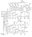
- FIG. 2 is a circuit diagram illustrating a specific configuration example of the failure detection unit 40.
- the base-emitter voltages Vbe of the respective transistors are all equal.
- the switch 91 includes four 2-input 1-output switches.
- One four inputs in the switch 91 are connected to the monitor paths P1 to P4 described above in FIG. 1, respectively, and the other four inputs are connected in common to the reference power supply Eref described in FIG.
- the emitter terminals of the transistors Q11, Q12, Q13, and Q14 are connected to the power supply Ed through the current sources I1, I2, I3, and I4, respectively, and the collector terminals are commonly grounded, thereby providing four emitter followers. Is configured. Further, the base terminals of the transistors Q11 to Q14 are connected to the four outputs of the switch 91, respectively.
- the base terminals of the transistors Q15, Q16, Q17, and Q18 are connected to the emitter terminals of the transistors Q11 to Q14, respectively, and the collector terminals are commonly connected to the power supply Ed.
- the emitter terminals of the transistors Q15 to Q18 are commonly grounded via the current source I5 and are connected to the base terminal of the transistor Q30.
- the switch 92 includes four switches with two inputs and one output. One four inputs in the switch 92 are connected to the monitor paths P1 to P4 described above in FIG. 1, respectively, and the other four inputs are connected in common to the power supply Ed.
- the emitter terminals of the transistors Q21, Q22, Q23, and Q24 are commonly connected to the power supply Ed via the current source I10, the collector terminals are commonly grounded, and the base terminals are connected to the four outputs of the switch 92, respectively. .
- the base terminal of the transistor Q25 constituting the emitter follower is connected to the emitter terminals of the transistors Q21 to Q24, the collector terminal is connected to the power supply Ed, and the emitter terminal is grounded via the current source I11.
- the base terminal of the transistor Q26 is connected to the emitter terminal of the transistor Q25, the collector terminal is grounded, the emitter terminal is connected to one end of the resistor R10, and the other end of the resistor R10 is connected to the power supply Ed via the current source I12.
- Transistors Q30, Q31, Q32, and Q33 and constant current source I6 have a base terminal of transistor Q30 as a non-inverting input terminal, a base terminal of transistor Q31 as an inverting input terminal, and a collector terminal of transistor Q31 as an output terminal.
- a differential amplifier circuit is configured.
- the switch 91 is controlled based on the drive current control signal V90 from the path P90, and selects the monitor voltage Vn1 to Vn4 or the reference voltage Vref.
- the drive current control signal V90 is at a high level.
- the switch 91 selects the monitor voltages Vn1 to Vn4 when the drive current control signal V90 is at a high level.
- Transistors Q15-Q18 receive monitor voltages Vn1-Vn4 at their base terminals, respectively. Since the transistors Q15 to Q18 operate so that only the transistor having the maximum base voltage at the base terminal is turned on, the maximum monitor voltage Vmax described above in FIG. 1 is generated at the base terminal of the transistor Q30.
- Switch 92 is controlled based on drive current control signal V90 from path P90, and selects monitor voltages Vn1 to Vn4 or voltage Vdd.
- the switch 92 selects the monitor voltages Vn1 to Vn4 when the drive current control signal V90 is at a high level. Since the transistors Q21 to Q24 operate so that only the transistor having the minimum base voltage at the base terminal is turned on, the minimum monitor voltage Vmin described in FIG. 1 is generated at the base terminal of the transistor Q26.
- the above-described differential amplifier circuit receives the maximum monitor voltage Vmax at the base terminal (non-inverting input terminal) of the transistor Q30 and the sum voltage Va at the base terminal (inverting input terminal) of the transistor Q31, causing a failure at the collector terminal of the transistor Q31. A detection signal Vdet is generated.
- Vdet ⁇ Vdd when Vmax> Va Vdet ⁇ 0 when Vmax ⁇ Va
- Vdet ⁇ 0 when Vmax ⁇ Va Vdet ⁇ 0 when Vmax ⁇ Va
- Vmax Vref + Vx (5)
- the minimum detection unit 42 does not necessarily generate the minimum monitor voltage Vmin as the minimum value of the monitor voltages Vn1 to Vn4.
- the minimum monitor voltage Vmin may be not less than the minimum value among the monitor voltages Vn1 to Vn4 and not more than the next largest monitor voltage after the maximum monitor voltage Vmax.
- the minimum monitor voltage Vmin may be the second largest monitor voltage or the second smallest monitor voltage among the monitor voltages Vn1 to Vn4. That is, if the minimum detection part 42 is the structure which can output a voltage smaller than the forward voltage Vd1 which the light emitting element with which the short circuit failure had had rather than the maximum monitor voltage Vmax produced
- the minimum detection part 42 is the structure which can output a voltage smaller than the forward voltage Vd1 which the light emitting element with which the short circuit failure had had rather than the maximum monitor voltage Vmax produced
- it is not limited to the configuration
- the failure detection unit 40 detects that the difference value between the maximum monitor voltage Vmax and the minimum monitor voltage Vmin is equal to or higher than the reference voltage Vth for a predetermined time.
- a configuration having a timer function may be adopted.
- the failure detection unit 40 and the power supply control unit 50 have a minimum detection unit 42 and a minimum detection unit 51, respectively. However, if both the minimum detection unit 42 and the minimum detection unit 51 are configured to detect the minimum monitor voltage among the monitor voltages Vn1 to Vn4, the output of any one of the minimum detection units is used as the failure detection unit 40 and the power supply control. It may be shared by the unit 50. In that case, the circuit area for one minimum detection unit can be reduced.
- the failure detection unit 40 detects a failure of the light emitting element based on the comparison between the monitor voltages Vn1 to Vn4.
- fluctuations in the monitor voltages Vn1 to Vn4 caused by fluctuations in the drive voltage Vout for driving the light emitting elements can be canceled as in-phase components, and only fluctuations in the monitor voltages Vn1 to Vn4 due to the failed light emitting elements are detected. can do. In this way, it is possible to prevent erroneous detection and reliably and easily detect a failure of the light emitting element.
- the numbers described above are exemplified for specifically explaining the present invention, and the present invention is not limited to the illustrated numbers.
- the logic levels represented by the high level / low level are exemplified for specifically explaining the present invention, and if the configuration of the logic circuit is changed, a combination of logic levels different from the exemplified logic level is used. Thus, it is possible to obtain an equivalent result.
- the component configured by hardware can be configured by software, and the component configured by software can also be configured by hardware.
- the present invention can be used for a light emitting element driving device.
Landscapes
- Engineering & Computer Science (AREA)
- Physics & Mathematics (AREA)
- Computer Hardware Design (AREA)
- General Physics & Mathematics (AREA)
- Theoretical Computer Science (AREA)
- Circuit Arrangement For Electric Light Sources In General (AREA)
- Led Devices (AREA)
Abstract
L'invention porte sur un dispositif d'attaque d'élément électroluminescent dans lequel des défauts de court-circuit et des défauts de circuit ouvert dans des éléments électroluminescents utilisés dans la source de lumière de rétroéclairage ou autre composant d'une télévision à écran à cristaux liquides (LCD-TV) peuvent être détectés de façon fiable et aisée. Des tensions au niveau des points de connexion entre un circuit d'attaque et des lignes d'éléments électroluminescents connectés en série sont surveillées, et la tension différentielle entre la sortie d'une unité de détection de maximum (41), qui détecte la tension surveillée maximale parmi les tensions surveillées, et la sortie d'une unité de détection de minimum (42), qui détecte la tension surveillée minimale parmi les tensions surveillées, est comparée à une tension de référence prédéterminée. Des courts-circuits ou des circuits ouverts sont détectés sur la base du résultat de comparaison.
Priority Applications (2)
| Application Number | Priority Date | Filing Date | Title |
|---|---|---|---|
| US13/314,597 US8878445B2 (en) | 2009-06-09 | 2011-12-08 | Light-emitting element driving device |
| US14/496,213 US9237627B2 (en) | 2009-06-09 | 2014-09-25 | Light-emitting element driving device |
Applications Claiming Priority (2)
| Application Number | Priority Date | Filing Date | Title |
|---|---|---|---|
| JP2009138038A JP2010287601A (ja) | 2009-06-09 | 2009-06-09 | 発光素子駆動装置 |
| JP2009-138038 | 2009-06-09 |
Related Child Applications (1)
| Application Number | Title | Priority Date | Filing Date |
|---|---|---|---|
| US13/314,597 Continuation US8878445B2 (en) | 2009-06-09 | 2011-12-08 | Light-emitting element driving device |
Publications (1)
| Publication Number | Publication Date |
|---|---|
| WO2010143338A1 true WO2010143338A1 (fr) | 2010-12-16 |
Family
ID=43308601
Family Applications (1)
| Application Number | Title | Priority Date | Filing Date |
|---|---|---|---|
| PCT/JP2010/001493 Ceased WO2010143338A1 (fr) | 2009-06-09 | 2010-03-04 | Dispositif d'attaque d'élément électroluminescent |
Country Status (3)
| Country | Link |
|---|---|
| US (2) | US8878445B2 (fr) |
| JP (1) | JP2010287601A (fr) |
| WO (1) | WO2010143338A1 (fr) |
Cited By (5)
| Publication number | Priority date | Publication date | Assignee | Title |
|---|---|---|---|---|
| EP2493268A1 (fr) * | 2011-02-25 | 2012-08-29 | Toshiba Lighting & Technology Corporation | Dispositif d'éclairage et luminaire |
| CN103400553A (zh) * | 2013-07-26 | 2013-11-20 | 深圳市华星光电技术有限公司 | Led背光驱动电路以及液晶显示器 |
| WO2013175862A1 (fr) * | 2012-05-25 | 2013-11-28 | シャープ株式会社 | Appareil de commande de del, récepteur de télévision, et appareil d'éclairage |
| TWI674752B (zh) * | 2018-12-03 | 2019-10-11 | 新唐科技股份有限公司 | 驅動保護電路及操作電路 |
| US12307950B2 (en) * | 2021-07-22 | 2025-05-20 | Samsung Electronics Co., Ltd. | Display device and method for controlling same |
Families Citing this family (52)
| Publication number | Priority date | Publication date | Assignee | Title |
|---|---|---|---|---|
| TWI418247B (zh) * | 2010-12-06 | 2013-12-01 | Leadtrend Tech Corp | 積體電路、控制方法、與光源提供系統 |
| KR101712676B1 (ko) * | 2011-02-18 | 2017-03-07 | 매그나칩 반도체 유한회사 | Pwm 제어 회로 및 이를 이용한 led 구동회로 |
| KR102063739B1 (ko) * | 2011-03-31 | 2020-01-09 | 온세미컨덕터코리아 주식회사 | Led 발광 장치의 구동 장치 및 구동 방법 |
| KR101847211B1 (ko) * | 2011-08-30 | 2018-04-10 | 매그나칩 반도체 유한회사 | Led구동장치 |
| JP5879132B2 (ja) * | 2012-01-12 | 2016-03-08 | シャープ株式会社 | 発光装置の異常検出装置および発光装置の異常検出方法 |
| JP5576892B2 (ja) | 2012-03-13 | 2014-08-20 | オムロンオートモーティブエレクトロニクス株式会社 | Led点灯および断線検出制御装置 |
| JP5576891B2 (ja) | 2012-03-13 | 2014-08-20 | オムロンオートモーティブエレクトロニクス株式会社 | Led点灯および断線検出制御装置 |
| JP2013203146A (ja) * | 2012-03-27 | 2013-10-07 | Ichikoh Ind Ltd | 車両用灯具 |
| FR2991121B1 (fr) * | 2012-05-25 | 2015-11-27 | Valeo Etudes Electroniques | Circuit de pilotage de l'alimentation d'une charge, notamment d'une diode d'affichage electroluminescente |
| CA2876646C (fr) * | 2012-06-13 | 2017-09-05 | Adb Airfield Solutions | Papi a led dote d'une protection contre la condensation |
| JP5363620B1 (ja) * | 2012-06-18 | 2013-12-11 | シャープ株式会社 | Led駆動装置、及びテレビジョン受像機 |
| WO2014013452A2 (fr) * | 2012-07-19 | 2014-01-23 | Koninklijke Philips N.V. | Dispositif d'éclairage à circuit de surveillance |
| US9119270B2 (en) * | 2012-10-04 | 2015-08-25 | Osram Sylvania Inc. | Solid state lighting device and driver configured for failure detection and recovery |
| CN105027678B (zh) * | 2012-11-21 | 2018-07-20 | 港大科侨有限公司 | 电流镜电路及方法 |
| JP5988214B2 (ja) * | 2012-12-04 | 2016-09-07 | パナソニックIpマネジメント株式会社 | 点灯装置およびそれを用いた照明器具 |
| JP5880467B2 (ja) | 2013-02-04 | 2016-03-09 | ソニー株式会社 | コンパレータ装置、並びに、表示装置及びその駆動方法 |
| US9269306B2 (en) * | 2013-03-29 | 2016-02-23 | Shenzhen China Star Optoelectronics Technology Co., Ltd | Backlight driving circuit, LCD device, and method for driving the backlight driving circuit |
| JP2014220200A (ja) * | 2013-05-10 | 2014-11-20 | キヤノン株式会社 | 照明装置及びその制御方法 |
| CN103295552B (zh) * | 2013-06-18 | 2015-07-15 | 深圳市华星光电技术有限公司 | 一种led背光驱动电路和背光驱动方法 |
| JP6234154B2 (ja) * | 2013-10-15 | 2017-11-22 | 三菱電機株式会社 | 光源制御装置及び光源制御方法 |
| CN103531156B (zh) * | 2013-10-25 | 2016-06-29 | 深圳市华星光电技术有限公司 | 背光驱动电路以及液晶显示装置 |
| DE102013222226B3 (de) * | 2013-10-31 | 2015-04-16 | Osram Gmbh | Schaltungsanordnung zum Betreiben mindestens einer ersten und einer zweiten Kaskade von LEDs |
| FR3013554A1 (fr) * | 2013-11-21 | 2015-05-22 | Valeo Illuminacion | Dispositif lumineux, notamment d'eclairage et/ou de signalisation d'un vehicule automobile |
| KR102208881B1 (ko) * | 2014-03-20 | 2021-01-28 | 삼성전자주식회사 | 백라이트 유닛, 백라이트 유닛을 포함하는 디스플레이 장치 및 그 구동 방법 |
| FR3018988A1 (fr) * | 2014-03-21 | 2015-09-25 | Valeo Iluminacion Sa | Systeme de pilotage de l'alimentation electrique d'une pluralite de sources lumineuses |
| US20150351170A1 (en) * | 2014-05-28 | 2015-12-03 | Screen Labs America, Inc. | Methods systems and devices for minimizing power losses in light emitting diode drivers |
| JP2016009537A (ja) * | 2014-06-23 | 2016-01-18 | 三菱電機株式会社 | 光源制御装置および光源制御方法 |
| EP3166218B1 (fr) * | 2014-07-04 | 2021-12-01 | Fuji Electric Co., Ltd. | Convertisseur de puissance |
| EP2979954B1 (fr) | 2014-07-29 | 2020-12-23 | Pintsch GmbH | Unite del pour emetteur de signaux lumineux, emetteur de signaux lumineux ayant une telle unite et procede de surveillance d'une chaine de del d'une unite del |
| CN104821156B (zh) * | 2015-05-19 | 2018-03-02 | 深圳市华星光电技术有限公司 | 一种led背光驱动电路 |
| US9989574B2 (en) * | 2015-05-27 | 2018-06-05 | Infineon Technologies Ag | System and method for short-circuit detection in load chains |
| JP6635689B2 (ja) * | 2015-06-23 | 2020-01-29 | ローム株式会社 | 照明装置、そのコントロール回路、制御方法、ならびにそれを用いたディスプレイ装置 |
| US10093232B2 (en) | 2015-09-16 | 2018-10-09 | Truck-Lite Co., Llc | Telematics road ready system |
| US10388161B2 (en) | 2015-09-16 | 2019-08-20 | Truck-Lite Co., Llc | Telematics road ready system with user interface |
| WO2017094555A1 (fr) * | 2015-11-30 | 2017-06-08 | シャープ株式会社 | Procédé d'évaluation d'un rétroéclairage à del |
| US20190268675A1 (en) | 2017-03-15 | 2019-08-29 | Scott Troutman | Telematics Road Ready System including a Bridge Integrator Unit |
| TWI625532B (zh) * | 2017-03-21 | 2018-06-01 | 失效偵測系統及其方法 | |
| CN106683605A (zh) * | 2017-03-31 | 2017-05-17 | 京东方科技集团股份有限公司 | 失效像素检测电路、方法和显示装置 |
| US10187955B2 (en) * | 2017-06-09 | 2019-01-22 | Infineon Technologies Ag | Detection of single short-LED in LED chains |
| US10383186B2 (en) * | 2017-08-10 | 2019-08-13 | Apple Inc. | Load transient response control systems and methods for electronic device displays |
| US10571516B2 (en) * | 2017-08-30 | 2020-02-25 | Arm Limited | CMOS process skew sensor |
| DE112018006777B4 (de) * | 2018-01-05 | 2022-06-15 | Rohm Co., Ltd. | Vielfach-abgabe-last-treibereinrichtung |
| KR101978708B1 (ko) * | 2018-04-19 | 2019-08-29 | 온세미컨덕터코리아 주식회사 | Led 발광 장치 |
| US10834795B2 (en) * | 2018-05-16 | 2020-11-10 | Hisense Visual Technology Co., Ltd. | Backlight drive circuit, backlight driving method, and display device |
| DE102018131803B4 (de) * | 2018-12-11 | 2025-12-11 | Infineon Technologies Ag | Verfahren zum detektieren eines defekts in einer led-kette und elektronische schaltung mit wenigstens einer led-kette |
| US11039518B2 (en) * | 2018-12-18 | 2021-06-15 | Mtd Products Inc | Method for LED fault detection and mechanism having LED fault detection |
| JP2020149831A (ja) * | 2019-03-13 | 2020-09-17 | ソニーセミコンダクタソリューションズ株式会社 | 故障検出装置、発光駆動装置および発光装置 |
| EP3838671A1 (fr) * | 2019-12-16 | 2021-06-23 | ZKW Group GmbH | Système de circuit |
| US11178742B1 (en) | 2020-07-15 | 2021-11-16 | Apple Inc. | Minimum voltage detector circuit |
| WO2022058230A1 (fr) | 2020-09-15 | 2022-03-24 | Signify Holding B.V. | Circuit d'attaque de del hybride |
| US12293698B2 (en) * | 2022-04-26 | 2025-05-06 | Fuzhou Boe Optoelectronics Technology Co., Ltd. | Method for driving light-emitting substrate with light-emitting sub-regions, driving circuit and display apparatus |
| CN114999357B (zh) * | 2022-04-28 | 2025-03-25 | 深圳市洲明科技股份有限公司 | Led灯珠自动检修方法、设备、存储介质及显示屏 |
Citations (3)
| Publication number | Priority date | Publication date | Assignee | Title |
|---|---|---|---|---|
| JP2008130513A (ja) * | 2006-11-24 | 2008-06-05 | Matsushita Electric Works Ltd | Led点灯回路およびそれを用いる照明器具 |
| JP2008305941A (ja) * | 2007-06-07 | 2008-12-18 | Pioneer Electronic Corp | 発光ダイオードのドライバ回路及び発光ダイオードの異常検出方法等 |
| JP2008311602A (ja) * | 2007-05-17 | 2008-12-25 | Seiko Npc Corp | Led駆動回路 |
Family Cites Families (6)
| Publication number | Priority date | Publication date | Assignee | Title |
|---|---|---|---|---|
| US7948468B2 (en) * | 2007-02-23 | 2011-05-24 | The Regents Of The University Of Colorado | Systems and methods for driving multiple solid-state light sources |
| EP1965609A3 (fr) * | 2007-02-27 | 2011-06-15 | Lumination, LLC | Détection de défaillance de chaîne DEL |
| US8129916B2 (en) * | 2008-09-26 | 2012-03-06 | Cypress Semiconductor Corporation | Light emitting driver circuit with bypass and method |
| US8174170B1 (en) * | 2009-05-13 | 2012-05-08 | Sand 9, Inc. | Methods and apparatus for mechanical resonating structures |
| US8253339B1 (en) * | 2010-07-16 | 2012-08-28 | Kedar Godbole | Lighting element failure detection devices and methods for power switching based systems |
| JP2013021117A (ja) * | 2011-07-11 | 2013-01-31 | Rohm Co Ltd | Led駆動装置、照明装置、液晶表示装置 |
-
2009
- 2009-06-09 JP JP2009138038A patent/JP2010287601A/ja active Pending
-
2010
- 2010-03-04 WO PCT/JP2010/001493 patent/WO2010143338A1/fr not_active Ceased
-
2011
- 2011-12-08 US US13/314,597 patent/US8878445B2/en active Active
-
2014
- 2014-09-25 US US14/496,213 patent/US9237627B2/en active Active
Patent Citations (3)
| Publication number | Priority date | Publication date | Assignee | Title |
|---|---|---|---|---|
| JP2008130513A (ja) * | 2006-11-24 | 2008-06-05 | Matsushita Electric Works Ltd | Led点灯回路およびそれを用いる照明器具 |
| JP2008311602A (ja) * | 2007-05-17 | 2008-12-25 | Seiko Npc Corp | Led駆動回路 |
| JP2008305941A (ja) * | 2007-06-07 | 2008-12-18 | Pioneer Electronic Corp | 発光ダイオードのドライバ回路及び発光ダイオードの異常検出方法等 |
Cited By (7)
| Publication number | Priority date | Publication date | Assignee | Title |
|---|---|---|---|---|
| EP2493268A1 (fr) * | 2011-02-25 | 2012-08-29 | Toshiba Lighting & Technology Corporation | Dispositif d'éclairage et luminaire |
| US8643307B2 (en) | 2011-02-25 | 2014-02-04 | Toshiba Lighting & Technology Corporation | Lighting device and luminaire |
| WO2013175862A1 (fr) * | 2012-05-25 | 2013-11-28 | シャープ株式会社 | Appareil de commande de del, récepteur de télévision, et appareil d'éclairage |
| CN103400553A (zh) * | 2013-07-26 | 2013-11-20 | 深圳市华星光电技术有限公司 | Led背光驱动电路以及液晶显示器 |
| TWI674752B (zh) * | 2018-12-03 | 2019-10-11 | 新唐科技股份有限公司 | 驅動保護電路及操作電路 |
| US11095112B2 (en) | 2018-12-03 | 2021-08-17 | Nuvoton Technology Corporation | Driving protection circuit, operating circuit and control method |
| US12307950B2 (en) * | 2021-07-22 | 2025-05-20 | Samsung Electronics Co., Ltd. | Display device and method for controlling same |
Also Published As
| Publication number | Publication date |
|---|---|
| US20150022089A1 (en) | 2015-01-22 |
| US9237627B2 (en) | 2016-01-12 |
| US8878445B2 (en) | 2014-11-04 |
| JP2010287601A (ja) | 2010-12-24 |
| US20120074856A1 (en) | 2012-03-29 |
Similar Documents
| Publication | Publication Date | Title |
|---|---|---|
| WO2010143338A1 (fr) | Dispositif d'attaque d'élément électroluminescent | |
| US8144111B2 (en) | Light emitting diode driving circuit having voltage detection | |
| US8169156B2 (en) | Control method capable of preventing flicker effect and light emitting device thereof | |
| US20100225622A1 (en) | Driving apparatus | |
| US11019700B2 (en) | LED driving system and LED driving device | |
| US8502459B2 (en) | Driver IC for electrical load and driving method thereof | |
| JP2008258428A (ja) | 照明用白色led駆動回路並びにこれを備えた照明装置及び電子機器 | |
| JP2010063332A (ja) | 負荷駆動装置 | |
| JP2010212369A (ja) | Led駆動装置 | |
| US8400075B2 (en) | Illumination circuit having bypass circuit controllable according to voltage change of series circuit thereof | |
| US12376209B2 (en) | Controller for controlling a light source module | |
| CN111986625A (zh) | 背光驱动电路及显示装置 | |
| KR101242423B1 (ko) | 발광소자 구동 장치, 구동 회로 및 그 회로의 구동 방법 | |
| JP5482617B2 (ja) | Led駆動電圧供給回路及びled装置 | |
| US20120038283A1 (en) | Light emitting diode driving system and circuit thereof | |
| US9232598B2 (en) | Operating circuit applied to backlight and associated method | |
| US8076863B2 (en) | Back light module | |
| US10945321B2 (en) | Light source apparatus and projection-type display apparatus | |
| JP4985870B1 (ja) | 定電流駆動装置およびそれを用いた負荷駆動装置 | |
| JP2015147445A (ja) | 車両用灯具およびその駆動装置 | |
| JP5214047B1 (ja) | Led点灯装置 | |
| JP5054236B1 (ja) | Led点灯装置 | |
| US11324100B2 (en) | Light source apparatus and projection-type display apparatus | |
| JP7549658B2 (ja) | 車両用灯具システム | |
| JP5149457B1 (ja) | Led点灯装置 |
Legal Events
| Date | Code | Title | Description |
|---|---|---|---|
| 121 | Ep: the epo has been informed by wipo that ep was designated in this application |
Ref document number: 10785870 Country of ref document: EP Kind code of ref document: A1 |
|
| NENP | Non-entry into the national phase |
Ref country code: DE |
|
| 122 | Ep: pct application non-entry in european phase |
Ref document number: 10785870 Country of ref document: EP Kind code of ref document: A1 |