WO2010143848A2 - 비스위칭 방식을 이용하는 램프 신호 발생기 및 이를 포함하는 이미지 센서 - Google Patents
비스위칭 방식을 이용하는 램프 신호 발생기 및 이를 포함하는 이미지 센서 Download PDFInfo
- Publication number
- WO2010143848A2 WO2010143848A2 PCT/KR2010/003631 KR2010003631W WO2010143848A2 WO 2010143848 A2 WO2010143848 A2 WO 2010143848A2 KR 2010003631 W KR2010003631 W KR 2010003631W WO 2010143848 A2 WO2010143848 A2 WO 2010143848A2
- Authority
- WO
- WIPO (PCT)
- Prior art keywords
- current
- signal
- capacitive element
- unit
- lamp signal
- Prior art date
- Legal status (The legal status is an assumption and is not a legal conclusion. Google has not performed a legal analysis and makes no representation as to the accuracy of the status listed.)
- Ceased
Links
Images


Classifications
-
- H—ELECTRICITY
- H03—ELECTRONIC CIRCUITRY
- H03K—PULSE TECHNIQUE
- H03K4/00—Generating pulses having essentially a finite slope or stepped portions
- H03K4/06—Generating pulses having essentially a finite slope or stepped portions having triangular shape
- H03K4/08—Generating pulses having essentially a finite slope or stepped portions having triangular shape having sawtooth shape
-
- H—ELECTRICITY
- H03—ELECTRONIC CIRCUITRY
- H03M—CODING; DECODING; CODE CONVERSION IN GENERAL
- H03M1/00—Analogue/digital conversion; Digital/analogue conversion
- H03M1/12—Analogue/digital converters
-
- H—ELECTRICITY
- H04—ELECTRIC COMMUNICATION TECHNIQUE
- H04N—PICTORIAL COMMUNICATION, e.g. TELEVISION
- H04N25/00—Circuitry of solid-state image sensors [SSIS]; Control thereof
-
- H—ELECTRICITY
- H04—ELECTRIC COMMUNICATION TECHNIQUE
- H04N—PICTORIAL COMMUNICATION, e.g. TELEVISION
- H04N25/00—Circuitry of solid-state image sensors [SSIS]; Control thereof
- H04N25/60—Noise processing, e.g. detecting, correcting, reducing or removing noise
- H04N25/618—Noise processing, e.g. detecting, correcting, reducing or removing noise for random or high-frequency noise
-
- H—ELECTRICITY
- H04—ELECTRIC COMMUNICATION TECHNIQUE
- H04N—PICTORIAL COMMUNICATION, e.g. TELEVISION
- H04N25/00—Circuitry of solid-state image sensors [SSIS]; Control thereof
- H04N25/70—SSIS architectures; Circuits associated therewith
- H04N25/76—Addressed sensors, e.g. MOS or CMOS sensors
- H04N25/78—Readout circuits for addressed sensors, e.g. output amplifiers or A/D converters
Definitions
- the present invention relates to a ramp signal generator for generating a ramp signal for analog-to-digital conversion and an image sensor comprising the same.
- image sensors formed by arranging a plurality of unit components (for example, pixels) that are sensitive to incident light in a line or matrix form are used in various fields. .
- an image sensor of a CCD (Charge Coupled Device) type, a metal oxide semiconductor (MOS) type, or a complementary metal-oxide semiconductor (CMOS) type that detects incident light is used. They read the amount of incident light converted by the unit component (pixel) into an electric signal as an electric signal.
- CCD Charge Coupled Device
- MOS metal oxide semiconductor
- CMOS complementary metal-oxide semiconductor
- Such an image sensor for example a CMOS image sensor, is a single tilt analog-to-digital converter (Analog / Digital Converter, hereinafter referred to as " ADC ") to read an analog electrical signal (photoelectric conversion signal) generated according to the light intensity. I'm using.
- the single slope ADC includes a ramp signal generator for generating a signal of a ramp waveform (hereinafter referred to as a “lamp signal”) as a reference signal for comparison with a photoelectric conversion signal.
- the conventional lamp signal generator is generally implemented by a method using a resistor DAC (Digital / Analog Converter) or a current steering DAC.
- a resistor DAC Digital / Analog Converter
- a current steering DAC outputs a digital signal input as an analog signal by a switching operation by a clock pulse.
- the conventional lamp signal generator has a problem of generating a lamp signal including switching noise according to the switching operation.
- the technical problem to be solved by an embodiment of the present invention is to provide a non-switching lamp signal generator and an image sensor using the same to solve the switching noise generation.
- an embodiment of the present invention is to provide a lamp signal generator and an image sensor for adjusting the slope of the lamp signal using the current mode and / or voltage mode to control the gain of the image sensor.
- the lamp signal generator for generating a ramp signal for analog-to-digital conversion, the reference power setting unit for setting a reference power; And a lamp signal generator for discharging the capacitive element after charging the prepared capacitive element using the reference power source and outputting a signal indicating a discharge trend of the charge as the lamp signal.
- the reference power setting unit may include a reference current supply unit supplying a reference current; And a reference voltage setting unit configured to set a reference voltage according to the reference current as the reference power source.
- the reference voltage setting unit may include a resistor unit connected to the reference current supply unit; And a buffer connected to the reference current supply unit and the resistor unit to receive a voltage applied across the resistor unit, and output the input voltage as the reference voltage.
- the reference current supply unit may be a bandgap circuit
- the resistor unit may be set to a resistor having the same process characteristics as that of the PTAT circuit of the bandgap circuit.
- the lamp signal generation unit may include the capacitive element charged using the reference power source; And a current source for discharging the charge charged in the capacitive element, and the lamp signal may indicate a discharge trend of the charge while the charge is discharged.
- the lamp signal generation unit comprises: a first switch to determine whether a short circuit between the reference power setting unit and the capacitive element; And a second switch to determine whether the charge is discharged.
- the supply current amount of the current source may be variable, and the change trend of the lamp signal may vary as the supply current amount of the current source is changed.
- the current source is a fixed current source for supplying a constant amount of current; And it may include a current mirror circuit for varying the amount of current input from the fixed current source.
- the ramp signal generator may include a voltage mode gain control unit configured to control an amount of change of the ramp signal over time using a non-inverting OP-Amp having an input terminal connected to one end of the capacitive element. It may further include. In this case, the ramp signal generator may further include a buffer positioned between the ramp signal generator and the voltage mode gain controller so that the operation of the voltage mode gain controller does not change the waveform of the ramp signal.
- the lamp signal generator may further include a filter connected to an input terminal of the voltage mode gain controller output terminal and removing noise of the lamp signal by using a transconductance amplifier and a capacitor.
- an image sensor includes a pixel array for converting the incident light into an electrical signal;
- a reference current supply unit for supplying a reference current, a reference voltage setting unit for setting a reference voltage according to the supplied reference current, a capacitive element connected to the reference voltage setting unit, and the set reference voltage applied to both ends to charge
- a current source connected to the reference voltage setting unit and the capacitive element to discharge a charge charged in the capacitive element to output a lamp signal.
- a comparator receiving the pixel signal and the ramp signal and comparing the two input signals to output a comparison signal;
- a counter for counting the input clock signal;
- a latch for receiving the comparison signal and storing and outputting a counter value of the counter according to the comparison signal.
- the current source may be set in a variable amount of supply current, and the change amount with respect to the time of the lamp signal may vary according to the variable setting of the amount of supply current in the current source.
- the present invention has an advantage of generating a switching signal in a non-switching manner, thereby eliminating switching noise.
- the present invention also has the advantage of overcoming the limitation of limitation of chip area and the improvement of the analog / digital converter (ADC) resolution of the image sensor by selectively or combining the current mode gain control and the voltage mode gain control.
- ADC analog / digital converter
- FIG. 1 is a schematic structural diagram of an image sensor according to an embodiment of the present invention.
- FIG. 2 is a block diagram of a lamp signal generator according to an embodiment of the present invention.
- FIG 3 is an exemplary view of a ramp signal according to an embodiment of the present invention.
- FIG. 4 is a circuit diagram of a current mode gain control unit according to an embodiment of the present invention.
- FIG. 5 is a circuit diagram of a voltage mode gain control unit according to an embodiment of the present invention.
- FIG. 6 is an exemplary diagram illustrating tilt adjustment of a ramp signal according to an embodiment of the present invention.
- comparator 140 latch
- reference current supply unit 220 reference voltage setting unit
- first switch 240 current mode gain control unit
- non-inverting voltage amplifier 530 filtering unit
- ordinal numbers such as second and first
- first and second components may be used to describe various components, but the components are not limited by the terms. The terms are used only for the purpose of distinguishing one component from another.
- second component may be referred to as the first component, and similarly, the first component may also be referred to as the second component.
- the present invention relates to a lamp signal generator 120 for generating a lamp signal in a non-switching manner and an image sensor using the same.
- the image sensor may include a CCD, a MOS, and a CMOS, but for convenience of understanding and description, the CMOS image sensor is described as a representative example, but is not limited thereto. Including all image sensors using).
- an image sensor may include a pixel array 110, a ramp signal generator 120, a comparator 130, a latch 140, a counter 150, and a timing controller 160. It includes.
- the image sensor of the present invention converts the accumulated charges into electric signals according to the light incident on the pixel array 110.
- the image sensor compares and reads the converted electrical signal and the reference signal (lamp signal).
- the pixel array 110 consists of a two-dimensional array of a plurality of pixels that receive light and convert it into an electrical signal.
- the electrical signal output from the pixel is transmitted to the input of the comparator 130 described later.
- the ramp signal generator 120 generates and outputs a ramp signal.
- the ramp signal is a signal of a ramp waveform (for example, the waveform of FIG. 3), and means a signal of a waveform which decreases (or increases) with a single slope.
- the lamp signal generator 120 of the present invention generates a lamp signal in a non-switching manner. Therefore, the lamp signal generator 120 of the present invention has an advantage that can fundamentally solve the switching noise problem.
- Ramp signal generator 120 of the present invention unlike the conventional resistance DAC or current steering DAC, generates a ramp signal that is constantly reduced with time by the capacitive element 242 and the current source in a non-switching manner.
- the comparator 130 receives a ramp signal and a pixel signal.
- the comparator 130 outputs a comparison signal according to a comparison result between the two input signals.
- the comparator 130 may compare an input pixel signal with a ramp signal, and output an instantaneous inversion logic value (a comparison signal, for example, changing from Logic0 to Logic1) when the ramp signal is lower than the pixel signal. .
- a comparison signal for example, changing from Logic0 to Logic1
- the counter 150 starts counting the clock signal at the moment when the comparator 130 starts the comparison, and the latch 140 at the time when the comparator 130 outputs the inverted logic value (comparison signal). Store and output the count value.
- the ramp signal generator 120, the comparator 130, the counter 150, and the latch 140, as described above, are components of a single slope ADC, and convert the analog signal into a digital signal through the above-described operation.
- the timing controller 160 performs a control function for sequentially reading pixel signals according to light incident on the pixel array 110.
- timing controller 160 may include a vertical / horizontal scan circuit and a timing pulse providing circuit.
- FIG. 2 is a block diagram of a lamp signal generator 120 according to an embodiment of the present invention.
- the lamp signal generator 120 includes a reference current supply unit 210, a reference voltage setting unit 220, a first switch 230, and a current mode gain control unit 240.
- the voltage mode gain controller 250 may be included.
- the reference power setting unit includes a reference current supply unit 210 and a reference voltage setting unit 220
- the lamp signal generation unit includes a first switch 230, a current mode gain control unit 240, and a voltage mode.
- the profit control unit 250 is made.
- the reference voltage setting unit 220 includes a resistor unit 222 and a buffer 224
- the current mode gain control unit 240 may include a capacitive element ( 242, second switch 244 and current source 246.
- the reference current supply unit 210 supplies a predetermined reference current to the reference voltage setting unit 220.
- the reference current supply unit 210 may be implemented as a bandgap circuit.
- the bandgap circuit is a circuit for outputting a predetermined reference current (or reference voltage), and the bandgap circuit is for reducing the influence of temperature (absolute temperature) change in order to output the reference current (or reference voltage) constantly. It includes a Proportional To Absolute Temperature (PTAT) circuit.
- PTAT Proportional To Absolute Temperature
- the reference voltage setting unit 220 sets the reference voltage according to the reference current input from the reference current supply unit 210.
- the reference voltage setting unit 220 includes a resistor 222 connected to an output terminal of the bandgap circuit, a bandgap circuit, and a buffer 224 connected to the resistor 222. can do.
- the resistor unit 222 may be set to a resistor having the same process characteristics as those of the above-described PTAT circuit in the bandgap circuit.
- the reference voltage setting unit 220 has an advantage of setting a stable voltage against process and temperature changes.
- the reference voltage is generated at both ends of the resistor unit 222 by the reference current, and the generated reference voltage is an input voltage of the buffer 224.
- the buffer 224 performs a function of maintaining the reference voltage so that it can be applied to both ends of the capacitive element 242 which will be described later.
- the voltage (ie, the reference voltage) of the buffer 224 is capacitive. It is applied to both ends of the element 242.
- the capacitive element 242 is charged with charge according to the applied reference voltage. That is, as the first switch 230 is closed, the capacitive element 242 charges a charge corresponding to the reference voltage.
- the capacitive element 242 and the current source 246 are connected, and the capacitive element 242 is connected by the current source 246. Discharge the charged charge.
- the applied voltage (initial reference voltage) across the capacitive element 242 is constantly reduced to show a ramp shape with a constant slope.
- the ramp signal is a signal that changes in proportion to the amount of charge remaining in the capacitive element.
- the ramp signal is generated while the capacitive element 242 is discharged by the current source 246 so that the reference voltage is constantly reduced.
- the reference voltage is set at both ends of the resistor unit 222, and the reference voltage set at the closing of the first switch 230 is applied to both ends of the capacitive element 242, thereby providing capacitive characteristics.
- Charge is charged to element 242.
- the first switch 230 is opened and the second switch 244 is closed, charges charged in the capacitive element 242 by the current source 246 are discharged to generate a lamp signal.
- the current mode gain control unit 240 including the capacitive element 242 and the current source 246 may vary the supply current amount of the current source 246, thereby inclining the ramp signal (that is, gain ( This is because Gain)) can be adjusted.
- FIG 3 is an exemplary diagram of a lamp signal according to an embodiment of the present invention.
- a ramp signal according to an embodiment of the present invention is a voltage signal having a constant slope with respect to time and decreasing.
- the ramp signal maintains the reference voltage until the time t1, and decreases with a constant slope from the time t1 to the time t2.
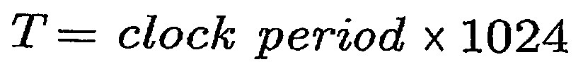
- the ramp signal is, for example, a voltage signal that stops decreasing and remains constant after t2 at the end of the 1024 clock cycles for a 10-bit single slope ADC.
- the amplitude Vramp of the ramp signal is the difference between the maximum reference voltage Vrefp and the voltage at which the reduction stops (Vrefn, the minimum value that can be reached during 1024 clock cycles).
- T is an operation period of the ramp waveform generator and is determined by the resolution of the ADC (including the lamp signal generator 120, the comparator 130, and the like).
- T becomes a value obtained by multiplying the clock period by 1024, as shown in Equation 2 below.
- the ramp signal V (t) over time may be expressed by Equation 3 below.
- FIG. 4 and 5 are circuit diagrams of the current mode gain control unit 240 and the voltage mode gain control unit 250 according to an embodiment of the present invention.
- FIG. 4 is an embodiment of the current mode gain control unit 240 that controls the slope (gain) of the ramp signal by varying the amount of current of the current source 246 using the current mirror 420
- FIG. 5 is a non-inverting voltage.
- An embodiment of the voltage mode gain control unit 250 that controls the slope (gain) of a ramp signal using an amplifier 520 (Non-inverting OP-Amp).
- CMOS parallel image sensors adjust gain by adjusting a slope of a ramp signal.
- the output value range of each photo cell may have a significantly smaller value than the amplitude of the ramp signal Vramp.
- the ramp signal is used (analog-to-digital conversion process), resulting in lower resolution of the ADC.
- the image sensor does not have good image quality and outputs a dark image.
- the ramp signal generator 120 needs to adjust the slope of the ramp signal.
- the lamp signal generator 120 of the present invention is capable of adjusting both the current mode gain control, the voltage mode gain control, and the gain through the combination of the current / voltage mode. First, the current mode gain adjustment will be described with reference to FIG. 4.
- the lamp signal generator 120 may adjust the gain of the lamp signal by adjusting the supply current amount of the current source 246 using the current mirror 420.
- the lamp signal generator 120 is configured such that the charge charged in the capacitive element 242 is discharged in accordance with the connection of the current source 246 (close of the second switch 244). Generate a signal.
- the ramp signal generator 120 may adjust the gain of the ramp signal by varying the amount of current supplied from the current source 246.
- the variable current source 246 may include a fixed current source 410 (a non-variable current supply) and a current mirror 420 using a plurality of transistors.
- the plurality of transistors apply a predetermined control signal (for example, a clock pulse of 5 bits) so that the on / off is controlled. Therefore, the ramp signal generator 120 may set the supply current amount I of the variable current source 246 using the input control signal (clock pulse).
- a predetermined control signal for example, a clock pulse of 5 bits
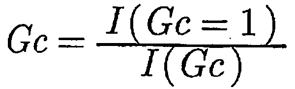
- the current mode gain control method using the variable current source 246 has its limitations.
- the gain of the ramp signal is increased by 32 times, the amount of current I of the current source 246 is reduced by 1/32 times. This can be seen through Equation 4 below.
- the present invention further proposes voltage mode gain control as well as current mode gain control.
- the ramp signal generator 120 may set the gain of the current mode gain control unit 240 to 4 times (Gc) and the gain of the voltage mode to 8 (Gv) times. This may be expressed as Equation 5 below.
- the voltage mode gain controller 250 may adjust the gain of the ramp signal by using the non-inverting voltage amplifier 520.
- the voltage mode gain control unit 250 which is an embodiment of the present invention, includes a plurality of buffer amplifiers 510 and B2 for maintaining a constant output voltage (lamp signal) from the capacitive element 242. May include resistors and an amplifier (OP-Amp).
- the buffer amplifier 510 serves to prevent the waveform of the ramp signal from being changed due to the operation of the voltage mode gain control unit.
- the voltage amplification gain Gv is determined according to the resistance values of the plurality of resistors by Equation 6 below.
- the gain of the ramp signal can be adjusted.
- the lamp signal generator 120 of the present invention may adjust the gain of the lamp signal by using the current mode and the voltage mode, respectively, or adjust the gain of the lamp signal through a combination of the two modes.
- the lamp signal generator 120 of the present invention has an advantage of designing the lamp signal generator 120 and the image sensor that are optimal for use considering the chip area limitation and considering the performance and the price.
- the lamp signal generator 120 of the present invention may further include a filter unit 530 at the output terminal of the voltage gain control unit to remove noise generated in various forms.
- the filtering unit 530 is a transconductance amplifier (A1) connected to the output terminal of the voltage gain control unit 532 and the correction capacitive element 534, one end of which is connected to the output terminal of the transconductance amplifier 532, C2) may be further included.
- the filtering unit 530 finally removes and outputs the noise included in the ramp signal.
- FIG. 6 is a diagram illustrating gain control of a ramp signal according to an embodiment of the present invention. Referring to FIG. 6, it can be seen that the slope of the ramp signal is adjusted according to the overall gain of the ramp signal generator 120.
- the ramp signal 1 610, the ramp signal 2 620, and the ramp signal 3 630 each have a slope (gain) according to the operation of the current mode gain control unit 240 and / or the voltage mode gain control unit 250 described above. To be controlled.
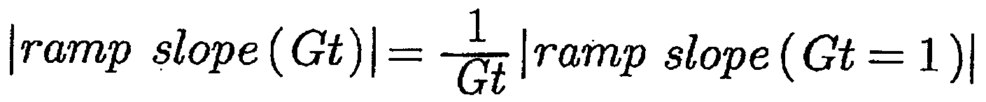
- a ramp slope of the ramp signal, a capacitance value C1 of the capacitive element 242, and a supply current value of the current source 246 ( I) the relationship between the amplitude of the ramp signal (Vramp), the ramp signal period (T) and the gain (Gt) of the ramp waveform generator is shown in [Equation 7], [Equation 8] and [Equation 9] below. same.
Landscapes
- Engineering & Computer Science (AREA)
- Multimedia (AREA)
- Signal Processing (AREA)
- Theoretical Computer Science (AREA)
- Transforming Light Signals Into Electric Signals (AREA)
- Analogue/Digital Conversion (AREA)
Abstract
본 발명은 비스위칭 방식을 이용하는 램프 신호 발생기 및 이를 포함하는 이미지 센서에 관한 것으로서, 본 발명의 일 측면에 따르면, 램프 신호 발생기가 개시된다. 아날로그-디지털 변환을 위한 램프 신호를 생성하는 본 발명의 일 실시예에 따른 램프 신호 발생기는, 기준전원을 설정하는 기준전원 설정부; 및 미리 마련된 용량성 소자를 기준전원을 이용해 충전시킨 후 용량성 소자를 방전시키며 상기 전하의 방전 추이를 나타내는 신호를 램프 신호로서 출력하는 램프신호 발생부를 포함한다. 본 발명에 의하면 비스위칭 방식으로 램프 신호를 생성하여, 스위칭 잡음 발생을 원천적으로 제거할 수 있는 장점이 있다.
Description
본 발명은 아날로그-디지털 변환을 위한 램프 신호를 생성하는 램프 신호 발생기 및 이를 포함하는 이미지 센서에 관한 것이다.
오늘날 전기 기기 관련 기술의 발달로, 입사된 광에 대하여 감응성을 갖는 단위 구성 요소(예를 들어, 픽셀(Pixel))를 라인 형상 혹은 매트릭스 형상으로 복수 개 배열하여 이루어지는 이미지 센서가 다양한 분야에서 사용되고 있다.
예를 들면, 영상 기기의 분야에서는 입사된 광을 검지하는 CCD(Charge Coupled Device)형 혹은 MOS(Metal Oxide Semiconductor)형이나 CMOS(Complementary Metal-oxide Semiconductor)형의 이미지 센서가 사용되고 있다. 이들은, 단위 구성 요소(픽셀)에 의해 전기 신호로 변환된 입사된 광량을 전기 신호로서 판독한다.
이러한 이미지 센서, 예를 들어 CMOS 이미지 센서는 빛의 세기에 따라서 발생된 아날로그 전기 신호(광전 변환 신호)를 판독하기 위해서 단일 기울기 아날로그-디지털 변환 장치(Analog/Digital Converter, 이하 “ADC”라 칭함)를 사용하고 있다. 이때, 단일 기울기 ADC는 광전 변환 신호와 비교하기 위한 기준 신호로 램프 파형의 신호(이하, “램프 신호”라 칭함)를 발생시키는 램프 신호 발생기를 포함하여 구현된다.
그런데 종래의 램프 신호 발생기는 일반적으로 저항 DAC(Digital/Analog Converter)나 전류 스티어링 DAC를 이용한 방식으로 구현되고 있다. 이러한 저항 DAC나, 전류 스티어링 DAC는 클럭 펄스(Clock Pulse)에 의한 스위칭 동작으로 입력된 디지털 신호를 아날로그 신호로 출력하는 것이다.
따라서 종래의 램프 신호 발생기는 이러한 스위칭 동작에 따라 스위칭 잡음이 포함된 램프 신호를 생성하는 문제점이 있었다.
이러한 스위칭 잡음은 영상 신호로 변환하는 과정에서 가로줄 잡음을 발생시켜 화질 저하의 근원이 되고 있다. 이러한 스위칭 잡음을 여과기(Filter)를 통하여 제거하는 노력이 있으나, 스위칭 잡음 발생의 근원적 해결은 되지 못하고 있는 현실이다.
본 발명의 일 실시예가 해결하고자 하는 기술적 과제는 스위칭 잡음 발생을 해결하는 비스위칭 방식의 램프 신호 발생기 및 이를 이용한 이미지 센서를 제공하는 것이다.
또한 본 발명의 일 실시예는 이미지 센서의 이득을 제어하기 위하여 전류 모드 및/또는 전압 모드를 사용하여 램프신호의 기울기를 조절하는 램프 신호 발생기 및 이미지 센서도 제공하고자 한다.
상기 과제를 이루기 위해, 아날로그-디지털 변환을 위한 램프 신호를 생성하는 본 발명의 일 실시예에 따른 램프 신호 발생기는, 기준전원을 설정하는 기준전원 설정부; 및 미리 마련된 용량성 소자를 상기 기준전원을 이용해 충전시킨 후 상기 용량성 소자를 방전시키며 상기 전하의 방전 추이를 나타내는 신호를 상기 램프 신호로서 출력하는 램프신호 발생부를 포함한다.
여기서, 상기 기준전원 설정부는 기준전류를 공급하는 기준전류 공급부; 및 상기 기준전류에 따른 기준전압을 상기 기준전원으로서 설정하는 기준전압 설정부를 포함할 수 있다.
여기서, 상기 기준전압 설정부는 상기 기준전류 공급부에 연결된 저항부; 및 상기 기준전류 공급부 및 상기 저항부에 연결되어, 상기 저항부 양단에 인가된 전압이 입력되고, 입력된 전압을 상기 기준전압으로서 출력하는 버퍼를 포함할 수 있다. 이 때, 상기 기준전류 공급부는 밴드갭(Bandgap) 회로이며, 상기 저항부는 상기 밴드갭 회로의 PTAT(Proportional To Absolute Temperature) 회로의 저항과 동일한 공정 특성을 갖는 저항으로 설정될 수 있다.
여기서, 상기 램프신호 발생부는 상기 기준전원을 이용하여 충전되는 상기 용량성 소자; 및 상기 용량성 소자에 충전된 전하를 방전시키는 전류원을 포함하고, 상기 램프 신호는 상기 전하가 방전되는 동안의 상기 전하의 방전 추이를 나타낼 수 있다. 이때 상기 램프 신호 발생부는 상기 기준전원 설정부 및 상기 용량성 소자간의 단락여부를 결정하는 제1 스위치; 및 상기 전하의 방전 여부를 결정하는 제2 스위치를 더 포함할 수 있다. 이때, 상기 전류원의 공급 전류량은 가변 가능하고, 상기 전류원의 공급 전류량이 가변됨에 따라 상기 램프 신호의 변화 추이가 가변될 수 있다. 이때, 상기 전류원은 일정한 전류량을 공급하는 고정 전류원; 및 상기 고정 전류원으로부터 입력된 전류량을 가변하는 전류 미러 회로를 포함할 수 있다.
여기서, 상기 램프 신호 발생기는 입력단이 상기 용량성 소자의 일단에 연결되는 비반전 전압 증폭기(Non-inverting OP-Amp)를 이용하여, 상기 램프 신호의 시간에 대한 변화량을 제어하는 전압 모드 이득 제어부를 더 포함할 수 있다. 이때, 램프 신호 발생기는 상기 램프 신호 발생부와 상기 전압모드 이득 제어부 사이에 위치하며, 상기 전압모드 이득 제어부의 동작이 상기 램프 신호의 파형을 변화시키지 않도록 하는 버퍼를 더 포함할 수 있다. 그리고 상기 램프 신호 발생기는 입력단이 상기 전압모드 이득 제어부 출력단에 연결되며, 트랜스 콘닥턴스 앰프(Transconductance Amp) 및 커패시터(Capacitor)를 이용하여 상기 램프 신호의 잡음을 제거하는 여과부를 더 포함할 수도 있다.
상기 과제를 이루기 위해, 본 발명의 일 실시예에 따른 이미지 센서는 입사된 광을 전기신호로 변환하는 픽셀어레이; 기준전류를 공급하는 기준전류 공급부, 상기 공급된 기준전류에 따라 기준전압이 설정되는 기준전압 설정부, 상기 기준전압 설정부에 연결되고 상기 설정된 기준전압이 양단에 인가되어 전하가 충전되는 용량성 소자 및 상기 기준전압 설정부 및 상기 용량성 소자에 연결되고 상기 용량성 소자에 충전된 전하를 방전시켜 램프 신호가 출력되도록 하는 전류원을 포함하는 램프 신호 발생기; 상기 픽셀 신호 및 상기 램프 신호를 입력받아, 입력된 두 신호를 비교하여 비교 신호를 출력하는 비교기; 입력된 클럭 신호를 계수하는 카운터; 및 상기 비교 신호를 입력받아, 상기 비교 신호에 따라 상기 카운터의 카운터값을 저장하여 출력하는 래치를 포함한다.
여기서, 상기 전류원은 공급 전류량의 가변 설정이 가능하고, 상기 전류원의 공급 전류량의 가변 설정에 따라, 상기 램프 신호의 시간에 대한 변화량이 가변될 수 있다.
따라서, 본 발명은 비스위칭 방식으로 램프 신호를 생성하여, 스위칭 잡음 발생을 제거하는 장점이 있다.
또한, 본 발명은 전류 모드 이득 제어 및 전압 모드 이득 제어를 선택적, 혹은 조합하여 이미지 센서의 ADC(Analog/Digital Converter) 분해능 향상 및 칩 면적의 제한 한계를 극복할 수 있는 장점도 있다.
도 1은 본 발명의 일 실시예에 따른 이미지 센서의 개략적 구성도.
도 2는 본 발명의 일 실시예에 따른 램프 신호 발생기의 구성도.
도 3은 본 발명의 일 실시예에 따른 램프 신호의 예시도.
도 4는 본 발명의 일 실시예에 따른 전류 모드 이득 제어부의 회로도.
도 5는 본 발명의 일 실시예에 따른 전압 모드 이득 제어부의 회로도.
도 6은 본 발명의 일 실시예에 따른 램프 신호의 기울기 조절 예시도.
<도면의 주요부분에 대한 부호의 설명>
110: 픽셀 어레이 120: 램프 신호 발생기
130: 비교기 140: 래치
150: 카운터 160: 타이밍 제어부
210: 기준전류 공급부 220: 기준전압 설정부
230: 제1 스위치 240: 전류 모드 이득 제어부
250: 전압 모드 이득 제어부 410: 고정 전류원
420: 전류 미러 회로 510: 제2 버퍼
520: 비반전 전압 증폭기 530: 여과부
본 발명은 다양한 변경을 가할 수 있고 여러 가지 실시예를 가질 수 있는 바, 특정 실시예들을 도면에 예시하고 상세한 설명에 상세하게 설명하고자 한다. 그러나, 이는 본 발명을 특정한 실시 형태에 대해 한정하려는 것이 아니며, 본 발명의 사상 및 기술 범위에 포함되는 모든 변경, 균등물 내지 대체물을 포함하는 것으로 이해되어야 한다.
제2, 제1 등과 같이 서수를 포함하는 용어는 다양한 구성요소들을 설명하는데 사용될 수 있지만, 상기 구성요소들은 상기 용어들에 의해 한정되지는 않는다. 상기 용어들은 하나의 구성요소를 다른 구성요소로부터 구별하는 목적으로만 사용된다. 예를 들어, 본 발명의 권리 범위를 벗어나지 않으면서 제2 구성요소는 제1 구성요소로 명명될 수 있고, 유사하게 제1 구성요소도 제2 구성요소로 명명될 수 있다. 및/또는 이라는 용어는 복수의 관련된 기재된 항목들의 조합 또는 복수의 관련된 기재된 항목들 중의 어느 항목을 포함한다.
어떤 구성요소가 다른 구성요소에 "연결되어" 있다거나 "접속되어" 있다고 언급된 때에는, 그 다른 구성요소에 직접적으로 연결되어 있거나 또는 접속되어 있을 수도 있지만, 중간에 다른 구성요소가 존재할 수도 있다고 이해되어야 할 것이다. 반면에, 어떤 구성요소가 다른 구성요소에 "직접 연결되어" 있다거나 "직접 접속되어" 있다고 언급된 때에는, 중간에 다른 구성요소가 존재하지 않는 것으로 이해되어야 할 것이다.
본 출원에서 사용한 용어는 단지 특정한 실시예를 설명하기 위해 사용된 것으로, 본 발명을 한정하려는 의도가 아니다. 단수의 표현은 문맥상 명백하게 다르게 뜻하지 않는 한, 복수의 표현을 포함한다. 본 출원에서, "포함하다" 또는 "가지다" 등의 용어는 명세서상에 기재된 특징, 숫자, 단계, 동작, 구성요소, 부품 또는 이들을 조합한 것이 존재함을 지정하려는 것이지, 하나 또는 그 이상의 다른 특징들이나 숫자, 단계, 동작, 구성요소, 부품 또는 이들을 조합한 것들의 존재 또는 부가 가능성을 미리 배제하지 않는 것으로 이해되어야 한다.
다르게 정의되지 않는 한, 기술적이거나 과학적인 용어를 포함해서 여기서 사용되는 모든 용어들은 본 발명이 속하는 기술 분야에서 통상의 지식을 가진 자에 의해 일반적으로 이해되는 것과 동일한 의미를 가지고 있다. 일반적으로 사용되는 사전에 정의되어 있는 것과 같은 용어들은 관련 기술의 문맥 상 가지는 의미와 일치하는 의미를 가지는 것으로 해석되어야 하며, 본 출원에서 명백하게 정의하지 않는 한, 이상적이거나 과도하게 형식적인 의미로 해석되지 않는다.
이하, 첨부된 도면을 참조하여 본 발명에 따른 바람직한 실시예를 상세히 설명하되, 도면 부호에 관계없이 동일하거나 대응하는 구성 요소는 동일한 참조 번호를 부여하고 이에 대한 중복되는 설명은 생략하기로 한다.
본 발명은 비스위칭 방식으로 램프 신호를 생성하는 램프 신호 발생기(120) 및 이를 이용하는 이미지 센서에 관한 것이다. 이미지 센서는 CCD, MOS, CMOS 등이 있으나, 본 명세서에서는 이해와 설명의 편의를 위하여, CMOS 이미지 센서를 대표적인 예로서 설명하나 이에 한정되지 않고 비스위칭 방식으로 램프 신호를 생성하는 램프 신호 발생기(120)를 이용하는 모든 이미지 센서를 포함한다.
도 1은 본 발명의 일 실시예에 따른 이미지 센서의 개략적 구성도이다. 도 1을 참조하면, 본 발명의 일 실시예에 따른 이미지 센서는 픽셀 어레이(110), 램프 신호 발생기(120), 비교기(130), 래치(140), 카운터(150), 타이밍 제어기(160)를 포함한다.
본 발명의 이미지 센서는 픽셀 어레이(110)에 입사된 광에 따라 축적된 전하를 전기 신호로 변환한다. 그리고 이미지 센서는 변환된 전기 신호와 기준 신호(램프 신호)를 비교하여 판독한다.
또한, 본 명세서는 이해와 설명의 편의를 위하여, 이미지 센서(혹은 램프 신호 발생기(120))의 구성을 기능별로 구분하여 설명하기로 한다. 따라서 실제 이미지 센서의 구현은 도 1에서 구분된 바와 다를 수 있을 수 있으나, 이러한 구분으로만 본 발명의 권리 범위가 한정되지 않음은 분명하다.
픽셀 어레이(110)는 빛을 받아서 전기신호로 변환하는 복수개의 픽셀들의 이차원 배열로 이루어진다. 픽셀에서 출력되는 전기신호는 이후에 설명되는 비교기(130)의 입력단에 전달된다.
램프 신호 발생기(120)는 램프 신호를 생성하여 출력한다. 여기서, 램프 신호는 램프 파형의 신호(예를 들어, 도 3의 파형)로서 단일 기울기를 가지고 감소(혹은 증가)하는 파형의 신호를 뜻한다.
본 발명의 램프 신호 발생기(120)는 비스위칭 방식으로 램프 신호를 생성한다. 따라서 본 발명의 램프 신호 발생기(120)는 스위칭 잡음 문제를 원천적으로 해결할 수 있는 장점이 있다.
본 발명의 램프 신호 발생기(120)는 종래의 저항 DAC나, 전류 스티어링 DAC와 달리, 비스위칭 방식으로 용량성 소자(242)와 전류원에 의하여 시간에 대하여 일정하게 감소하는 램프 신호를 생성한다.
램프 신호 발생기(120)의 구체적 구성 및 동작은 도 2의 설명에서 더 자세히 설명하기로 한다.
비교기(130)는 램프 신호와 픽셀 신호를 입력받는다. 그리고 비교기(130)는 입력된 두 신호의 비교 결과에 따라 비교 신호를 출력한다.
예를 들어, 비교기(130)는 입력된 픽셀 신호와 램프 신호를 비교하여, 램프 신호가 픽셀 신호보다 낮아지는 순간 반전 논리값(비교 신호, 예를 들어 Logic0에서 Logic1로 변경)을 출력할 수 있다.
이때, 카운터(150)는 비교기(130)가 비교를 시작하는 순간에 클럭 신호를 계수하기 시작하고, 래치(140)는 비교기(130)가 반전된 논리값(비교 신호)를 출력하는 시점에서의 계수값을 저장하여 출력한다.
상술한, 램프 신호 발생기(120), 비교기(130), 카운터(150) 및 래치(140)는 단일 기울기 ADC의 구성 요소로서, 상술한 동작을 통하여 아날로그신호를 디지털 신호로 변환하여 출력한다.
타이밍 제어기(160)는 픽셀 어레이(110)에 입사된 광에 따른 픽셀 신호를 순차적으로 판독하기 위한 제어 기능을 수행한다.
예를 들어, 타이밍 제어기(160)는 수직/수평 주사 회로 및 타이밍 펄스 제공 회로를 포함할 수 있다.
본 명세서는 본 발명에 직접 관련되지 않기 때문에 특별히 도시하지 않거나, 여러 구성 요소를 하나로(혹은 하나의 구성 요소를 여러 개로) 구분하여 기능적으로 설명하였으나, 본 발명은 이에 한정되지 않음은 자명하다.
지금까지 도 1을 참조하여 본 발명의 일 실시예에 따른 이미지 센서의 개략적 구성을 설명하였다. 이하, 도 2를 참조하여 램프 신호 발생기(120)의 구성에 대해서 상세히 설명하기로 한다.
도 2는 본 발명의 일 실시예에 따른 램프 신호 발생기(120)의 구성도이다.
도 2를 참조하면, 본 발명의 일 실시예에 따른 램프 신호 발생기(120)는 기준전류 공급부(210), 기준전압 설정부(220), 제1 스위치(230), 전류 모드 이득 제어부(240), 전압 모드 이득 제어부(250)를 포함할 수 있다. 설명의 편의상 본 명세서에서 기준전원 설정부는 기준전류 공급부(210) 및 기준전압 설정부(220)로 이루어지고, 램프신호 발생부는 제1 스위치(230), 전류 모드 이익 제어부(240), 및 전압 모드 이익 제어부(250)로 이루어진다. 한편, 도 2에 도시된 본 발명의 일 실시예에 따르면, 기준전압 설정부(220)는 저항부(222) 및 버퍼(224)로 이루어지며, 전류 모드 이득 제어부(240)은 용량성 소자(242), 제2 스위치(244) 및 전류원(246)으로 이루어진다.
이하, 도 2에서 도시한 바를 참조하여, 기준전류 공급부(210)에 의하여 기준전류의 공급을 시작으로 램프 신호가 발생하는 과정을 순차적으로 설명하도록 한다.
기준전류 공급부(210)는 소정의 기준전류를 기준전압 설정부(220)로 공급한다. 예를 들어, 기준전류 공급부(210)는 밴드갭(Bandgap) 회로로 구현될 수 있다.
여기서, 밴드갭 회로는 소정의 기준전류(혹은 기준전압)을 출력하는 회로이며, 밴드갭 회로는 기준전류(혹은 기준전압)를 일정하게 출력하기 위하여 온도(절대 온도) 변화에 의한 영향을 줄이기 위한 PTAT(Proportional To Absolute Temperature) 회로를 포함한다.
기준전압 설정부(220)는 기준전류 공급부(210)로부터 입력된 기준전류에 따라 기준전압을 설정한다. 예를 들어, 기준전압 설정부(220)는 도 2에서 도시한 바와 같이, 밴드갭 회로의 출력단과 연결된 저항부(222), 밴드갭 회로 및 저항부(222)에 연결된 버퍼(224)를 포함할 수 있다.
저항부(222)는 밴드갭 회로 내의 상술한 PTAT 회로의 저항과 동일한 공정 특성을 갖는 저항으로 설정할 수 있다. 이로써, 기준전압 설정부(220)는 공정(process)과 온도 변화에 대하여 안정된 전압을 설정할 수 있는 장점이 있다.
기준전압은 기준전류에 의하여 저항부(222)의 양단에 생성되고, 생성된 기준전압이 버퍼(224)의 입력 전압이다. 이때, 버퍼(224)는 기준전압이 후술할 용량성 소자(242)의 양단에 일정하게 인가될 수 있도록 유지하는 기능을 수행한다.
한편, 상술한 타이밍 제어기(160)에 의하여, 버퍼(224)와 용량성 소자(242) 사이에 위치한 제1 스위치(230)가 폐쇄되면, 버퍼(224)의 전압(즉, 기준전압)이 용량성 소자(242)의 양단에 인가된다.
용량성 소자(242)는 인가된 기준전압에 따라 전하가 충전된다. 즉, 제1 스위치(230)의 폐쇄에 따라 용량성 소자(242)는 기준전압에 대응하는 전하를 충전하게 된다.
이후, 제1 스위치(230)의 개방 및 제2 스위치(244)의 폐쇄로 인하여, 용량성 소자(242)와 전류원(246)이 연결되고, 전류원(246)에 의하여 용량성 소자(242)는 충전된 전하를 방전한다. 이로써, 용량성 소자(242) 양단의 인가 전압(초기는 기준전압)은 일정하게 감소하여 일정한 기울기의 램프 형태를 나타낸다.
즉, 램프 신호는 용량성 소자에 남아있는 전하량에 비례하여 변화하는 신호로서, 전류원(246)에 의하여 용량성 소자(242)가 방전되면서, 기준전압이 일정하게 감소하며 발생한다.
정리하면, 기준전류의 공급으로 인하여, 저항부(222)의 양단에 기준전압이 설정되고, 제1 스위치(230)의 폐쇄로 설정된 기준전압이 용량성 소자(242)의 양단에 인가되어 용량성 소자(242)에 전하가 충전된다. 그리고 제1 스위치(230) 개방 및 제2 스위치(244) 폐쇄 이후, 전류원(246)에 의하여 용량성 소자(242)에 충전된 전하는 방전되어, 램프 신호가 발생한다.
한편, 본 명세서에서 용량성 소자(242) 및 전류원(246)을 포함하여 전류 모드 이득 제어부(240)라 명명한 것은 전류원(246)의 공급 전류량을 가변함으로써, 램프 신호의 기울기(즉, 이득(Gain))를 조절할 수 있기 때문이다.
이러한, 램프 신호의 기울기(이득)을 조절하는 기술적 내용(즉, 전류 모드 이득 제어부(240) 및 전압 모드 이득 제어부(250)의 동작)은 도 4 및 도 5를 통하여 자세히 후술하도록 한다.
지금까지 도 2를 참조하여 램프 신호 발생기(120)의 구성을 설명하였다. 이하, 도 3을 참조하여 램프 신호 발생기(120)에 따라 발생된 램프 신호를 예를 들어 설명하기로 한다.
도 3은 본 발명의 일 실시예에 따른 램프 신호의 예시도이다.
도 3을 참조하면, 본 발명의 일 실시예에 따른 램프 신호는 시간에 대하여 일정한 기울기를 가지며 감소하는 전압 신호이다.
상세하게는, 램프 신호는 t1시점까지 기준전압을 유지하다가, t1시점부터 t2시점까지 일정한 기울기로 감소한다. 그리고 램프 신호는 예를 들어, 10 비트 단일 기울기 ADC의 경우 1024 클럭 주기가 끝나는 t2시점 이후에 감소를 멈추고 일정한 전압으로 유지되는 전압 신호이다.
도 2를 더 참조하여 램프 신호의 발생을 수식적으로 더 설명하도록 한다.
램프 신호의 진폭(Vramp)은 최대치인 기준전압(Vrefp)과 감소가 멈추었을 때의 전압(Vrefn, 1024 클럭 주기 동안에 이를 수 있는 최소값)의 차이이다. 이때, 램프 신호의 진폭(Vramp)은 용량성 소자(242)의 용량값(C1), 전류원(246)의 공급 전류값(I) 및 시간(T=t2 - t1)를 인자로 하기의 [수학식 1]에 의하여 결정된다.
[수학식 1]
[규칙 제26조에 의한 보정 06.07.2010]
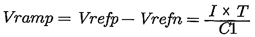
이때, T는 램프 파형 발생기의 동작구간으로, ADC(램프 신호 발생기(120), 비교기(130) 등을 포함)의 분해능(resolution)에 의하여 결정된다.
예를 들어, 10Bit ADC의 경우에 T는 하기의 [수학식 2]와 같이, 클럭의 주기에 1024를 곱한 값이 된다.
[수학식 2]
[규칙 제26조에 의한 보정 06.07.2010]
시간에 따른 램프 신호(V(t))는 하기의 [수학식 3]과 같이 수식적으로 표현될 수 있다.
[수학식 3]
[규칙 제26조에 의한 보정 06.07.2010]

지금까지 도 3을 참조하여 램프 신호 발생기(120)에 따라 발생된 램프 신호를 예를 들어 설명하였다. 이하, 도 4 및 도 5를 참조하여 램프 신호의 이득 조절 동작에 대해서 자세히 설명하기로 한다.
도 4 및 도 5는 본 발명의 일 실시예에 따른 전류 모드 이득 제어부(240) 및 전압 모드 이득 제어부(250)의 회로도이다. 도 4는 전류 미러(420)를 이용하여, 전류원(246)의 전류량을 가변함으로써 램프 신호의 기울기(이득)을 제어하는 전류 모드 이득 제어부(240)의 일 실시예이고, 도 5는 비반전 전압 증폭기(520)(Non-inverting OP-Amp)를 이용하여, 램프 신호의 기울기(이득)을 제어하는 전압 모드 이득 제어부(250)의 일 실시예이다.
일반적으로, 컬럼 병렬 방식의 CMOS형 이미지 센서는 램프 신호의 기울기를 조절하여 이득을 조절한다. 픽셀 어레이(110)에 입사된 광량이 적을 경우, 각 포토 셀들의 출력값 범위는 램프 신호의 진폭(Vramp)에 비하여 현저히 적은 값을 가질 수 있다. 이 경우, 램프 신호의 일부분만이 이용(아날로그/디지털 변환 과정)되어 결과적으로 ADC의 분해능을 낮추게 된다. 이로써, 이미지 센서는 화질이 좋지 않고 어두운 영상을 출력하게 된다.
따라서 ADC의 분해능 개선을 위해, 램프 신호 발생기(120)는 램프 신호의 기울기를 조절할 필요가 있다.
본 발명의 램프 신호 발생기(120)는 전류 모드 이득 조절, 전압 모드 이득 조절 및 전류/전압 모드의 조합을 통한 이득 조절이 모두 가능하다. 우선, 도 4를 참조하여 전류 모드 이득 조절을 설명하기로 한다.
도 4를 참조하면, 본 발명의 일 실시예에 따른 램프 신호 발생기(120)는 전류 미러(420)를 이용하여 전류원(246)의 공급 전류량을 조절함으로써 램프 신호의 이득을 조절할 수 있다.
이미 도 2의 설명에서 상술한 바와 같이, 램프 신호 발생기(120)는 용량성 소자(242)에 충전된 전하가 전류원(246)의 연결(제2 스위치(244)의 폐쇄)에 따라 방전됨으로써 램프 신호를 생성한다.
이때, 램프 신호 발생기(120)는 전류원(246)이 공급하는 전류량을 가변함으로서 램프 신호의 이득을 조절할 수 있다. 여기서, 가변 전류원(246)은 고정 전류원(410, 비가변 전류량 공급)과 복수의 트랜지스터를 이용한 전류 미러(420)(Current mirror)로 구성될 수 있다.
여기서, 복수의 트랜지스터는 소정의 제어 신호(예를 들어, 5bit의 클럭 펄스)를 인가하여 온/오프가 제어되도록 한다. 따라서 램프 신호 발생기(120)는 입력된 상기 제어 신호(클럭 펄스)로 가변 전류원(246)의 공급 전류량(I)을 설정할 수 있다.
한편, 가변 전류원(246)을 이용한 전류 모드 이득 제어 방식은 그 한계가 있다. 램프 신호의 이득을 32배로 증가시킨 경우, 전류원(246)의 전류량(I)은 1/32배로 줄어든다. 이는 하기의 [수학식 4]를 통하여 알 수 있다.
[수학식 4]
[규칙 제26조에 의한 보정 06.07.2010]
이 경우, 전류량이 감소는 신호 대 잡음비(SNR)가 나빠지는 원인이되며, 이를 해결하기 위해서는 용량성 소자(242)의 용량값(Cpacitance)를 키워야하는데, 이는 칩 면적 증가 및 생산 가격 증가로 이어진다.
따라서 본 발명은 전류 모드 이득 제어뿐만 아니라, 전압 모드 이득 제어를 추가로 제안한다.
즉, 램프 신호 발생기(120)가 32배의 전체 이득(Gt)이 필요한 경우, 전류 모드 이득 제어부(240)의 이득(Gc)을 1배로 설정하고, 전압 모드의 이득(Gv)을 32배로 설정할 수 있다. 또한, 램프 신호 발생기(120)는 전류 모드 이득 제어부(240)의 이득을 4배(Gc)로 설정하고, 전압 모드의 이득을 8(Gv)배로 설정할 수 있다. 이는 수식적으로 하기의 [수학식 5]와 같이 나타낼 수 있다.
[수학식 5]
[규칙 제26조에 의한 보정 06.07.2010]

이하, 도 5를 참조하여 전압 모득 이득 제어부의 회로도를 좀 더 자세히 설명하도록 한다.
본 발명의 일 실시예에 따른 전압 모드 이득 제어부(250)는 비반전 전압 증폭기(520)를 이용하여 램프 신호의 이득을 조절할 수 있다.
본 발명의 일 실시예인 전압 모드 이득 제어부(250)는 도 5에 도시한 바와 같이, 용량성 소자(242)로부터의 출력 전압(램프 신호)의 일정한 유지를 위한 버퍼 앰프(510, B2), 다수의 저항들 및 증폭기(OP-Amp)를 포함할 수 있다. 구체적으로, 버퍼 앰프(510)는 전압모드 이득 제어부의 동작으로 인하여 램프 신호의 파형을 변화시키지 않도록 하는 역할을 수행한다.
여기서, 전압 증폭 이득(Gv)은 하기의 [수학식 6]에 의하여 다수의 저항의 저항값에 따라 결정된다.
[수학식 6]
[규칙 제26조에 의한 보정 06.07.2010]

따라서 다수의 저항들의 저항값(Ra, Rb, Rc, Rd)을 설정(가변 저항 이용)함으로써, 램프 신호의 이득을 조절할 수 있다.
본 발명의 램프 신호 발생기(120)는 전류 모드와 전압 모드 각각을 이용하여 램프 신호의 이득을 조절하거나, 두 모드의 조합을 통하여 램프 신호의 이득을 조절할 수 있다. 이로써, 본 발명의 램프 신호 발생기(120)는 칩 면적 제한 한계를 고려한, 그리고 성능 및 가격을 고려한 사용 용도에 최적합한 램프 신호 발생기(120) 및 이미지 센서를 설계할 수 있는 장점이 있다.
한편, 본 발명의 램프 신호 발생기(120)는 다양한 형태로 발생한 잡음을 제거하기 위하여 전압 이득 제어부의 출력단에 여과부(530)를 더 포함시킬 수 있다.
여기서, 여과부(530)는 전압 이득 제어부의 출력단에 직렬로 연결되는 트랜스컨덕턴스 증폭기(532, Transconductance Amplifier, A1) 및 트랜스컨덕턴스 증폭기(532)의 출력단에 일단이 연결되는 보정 용량성 소자(534, C2)를 더 포함할 수 있다. 여과부(530)는 램프 신호에 포함된 잡음을 최종적으로 제거하고 출력하는 역할을 수행한다.
도 6은 본 발명의 일 실시예에 따른 램프 신호의 이득 제어 예시도이다. 도 6을 참조하면, 램프 신호의 기울기가 램프 신호 발생기(120)의 전체 이득에 따라 조절됨을 알 수 있다.
램프 신호 1(610), 램프 신호 2(620) 및 램프 신호 3(630) 각각은 상술한 전류 모드 이득 제어부(240) 및/또는 전압 모드 이득 제어부(250)의 동작에 따라 기울기(이득)가 조절되는 것을 나타낸다.
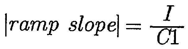
본 발명의 일 실시예에 따른 램프 신호 발생기(120)에서, 램프 신호의 기울기값(┃ramp slope┃), 용량성 소자(242)의 용량값(C1), 전류원(246)의 공급 전류값(I), 램프 신호의 진폭(Vramp), 램프 신호의 주기(T) 및 램프 파형 발생기의 이득(Gt)의 관계는 아래의 [수학식 7], [수학식 8] 및 [수학식 9]와 같다.
[수학식 7]
[규칙 제26조에 의한 보정 06.07.2010]

[수학식 8]
[규칙 제26조에 의한 보정 06.07.2010]
[수학식 9]
[규칙 제26조에 의한 보정 06.07.2010]
이상에서는 본 발명의 바람직한 실시예에 대하여 도시하고 설명하였지만, 본 발명은 상술한 특정의 실시예에 한정되지 아니하며, 청구범위에서 청구하는 본 발명의 요지를 벗어남이 없이 당해 발명이 속하는 기술 분야에서 통상의 지식을 가진 자에 의해 다양한 변형실시가 가능한 것은 물론이고, 이러한 변형실시들은 본 발명의 기술적 사상이나 전망으로부터 개별적으로 이해되어서는 안 될 것이다.
Claims (13)
- 아날로그-디지털 변환을 위한 램프 신호를 생성하는 램프 신호 발생기에 있어서,기준전원을 설정하는 기준전원 설정부; 및미리 마련된 용량성 소자를 상기 기준전원을 이용해 충전시킨 후 상기 용량성 소자를 방전시키며 상기 전하의 방전 추이를 나타내는 신호를 상기 램프 신호로서 출력하는 램프신호 발생부를 포함하는 램프 신호 발생기.
- 제1항에 있어서,상기 기준전원 설정부는기준전류를 공급하는 기준전류 공급부; 및상기 기준전류에 따른 기준전압을 상기 기준전원으로서 설정하는 기준전압 설정부를 포함하는 것을 특징으로 하는 램프 신호 발생기.
- 제2항에 있어서,상기 기준전압 설정부는상기 기준전류 공급부에 연결된 저항부; 및상기 기준전류 공급부 및 상기 저항부에 연결되어, 상기 저항부 양단에 인가된 전압이 입력되고, 입력된 전압을 상기 기준전압으로서 출력하는 버퍼를 포함하는 것을 특징으로 하는 램프 신호 발생기.
- 제3항에 있어서,상기 기준전류 공급부는 밴드갭(Bandgap) 회로이며,상기 저항부는 상기 밴드갭 회로의 PTAT(Proportional To Absolute Temperature) 회로의 저항과 동일한 공정 특성을 갖는 저항으로 설정되는 것을 특징으로 하는 램프 신호 발생기.
- 제1항에 있어서,상기 램프신호 발생부는상기 기준전원을 이용하여 충전되는 상기 용량성 소자; 및상기 용량성 소자에 충전된 전하를 방전시키는 전류원을 포함하고,상기 램프 신호는 상기 전하가 방전되는 동안의 상기 전하의 방전 추이를 나타내는 것을 특징으로 하는 램프 신호 발생기.
- 제5항에 있어서,상기 램프신호 발생부는상기 기준전원 설정부 및 상기 용량성 소자간의 단락여부를 결정하는 제1 스위치; 및상기 전하의 방전 여부를 결정하는 제2 스위치를 더 포함하는 램프 신호 발생기.
- 제5항에 있어서,상기 전류원의 공급 전류량은 가변 가능하고, 상기 전류원의 공급 전류량이 가변됨에 따라 상기 램프 신호의 기울기가 가변되는 것을 특징으로 하는 램프 신호 발생기.
- 제7항에 있어서,상기 전류원은일정한 전류량을 공급하는 고정 전류원; 및상기 고정 전류원으로부터 입력된 전류량을 가변하는 전류 미러 회로를 포함하는 것을 특징으로 하는 램프 신호 발생기.
- 제5항 또는 제7항에 있어서,입력단이 상기 용량성 소자의 일단에 연결되는 비반전 전압 증폭기(Non-inverting OP-Amp)를 이용하여, 상기 램프 신호의 시간에 대한 변화량을 제어하는 전압모드 이득 제어부를 더 포함하는 것을 특징으로 하는 램프 신호 발생기.
- 제9항에 있어서,상기 용량성 소자와 상기 전압모드 이득 제어부 사이에 위치하며, 상기 전압모드 이득 제어부의 동작이 상기 램프 신호의 파형을 변화시키지 않도록 하는 버퍼앰프(Buffer Amp)를 더 포함하는 것을 특징으로 하는 램프 신호 발생기.
- 제9항에 있어서,입력단이 상기 전압모드 이득 제어부 출력단에 연결되며, 트랜스 콘닥턴스 앰프(Transconductance Amp) 및 커패시터(Capacitor)를 이용하여 상기 램프 신호의 잡음을 제거하는 여과부를 더 포함하는 것을 특징으로 하는 램프 신호 발생기.
- 이미지 센서에 있어서,입사된 광을 전기신호로 변환하는 픽셀어레이;기준전류를 공급하는 기준전류 공급부, 상기 공급된 기준전류에 따라 기준전압이 설정되는 기준전압 설정부, 상기 기준전압 설정부에 연결되고 상기 설정된 기준전압이 양단에 인가되어 전하가 충전되는 용량성 소자 및 상기 기준전압 설정부 및 상기 용량성 소자에 병렬로 연결되고 상기 용량성 소자에 충전된 전하를 방전시켜 램프 신호가 출력되도록 하는 전류원을 포함하는 램프 신호 발생기;상기 픽셀 신호 및 상기 램프 신호를 입력받아, 입력된 두 신호를 비교하여 비교 신호를 출력하는 비교기;입력된 클럭 신호를 계수하는 카운터; 및상기 비교 신호를 입력받아, 상기 비교 신호에 따라 상기 카운터의 카운터값을 저장하여 출력하는 래치를 포함하는 이미지 센서.
- 제12항에 있어서,상기 전류원은 공급 전류량의 가변 설정이 가능하고, 상기 전류원의 공급 전류량의 가변 설정에 따라, 상기 램프 신호의 시간에 대한 변화량이 가변되는 것을 특징으로 하는 이미지 센서.
Applications Claiming Priority (2)
| Application Number | Priority Date | Filing Date | Title |
|---|---|---|---|
| KR1020090050465A KR20100131729A (ko) | 2009-06-08 | 2009-06-08 | 비스위칭 방식을 이용하는 램프 신호 발생기 및 이를 포함하는 이미지 센서 |
| KR10-2009-0050465 | 2009-06-08 |
Publications (3)
| Publication Number | Publication Date |
|---|---|
| WO2010143848A2 true WO2010143848A2 (ko) | 2010-12-16 |
| WO2010143848A3 WO2010143848A3 (ko) | 2011-03-03 |
| WO2010143848A8 WO2010143848A8 (ko) | 2011-04-28 |
Family
ID=43309340
Family Applications (1)
| Application Number | Title | Priority Date | Filing Date |
|---|---|---|---|
| PCT/KR2010/003631 Ceased WO2010143848A2 (ko) | 2009-06-08 | 2010-06-07 | 비스위칭 방식을 이용하는 램프 신호 발생기 및 이를 포함하는 이미지 센서 |
Country Status (2)
| Country | Link |
|---|---|
| KR (1) | KR20100131729A (ko) |
| WO (1) | WO2010143848A2 (ko) |
Families Citing this family (3)
| Publication number | Priority date | Publication date | Assignee | Title |
|---|---|---|---|---|
| KR20160114464A (ko) * | 2015-03-24 | 2016-10-05 | 현대아이에이치엘 주식회사 | 차량 램프의 전류 제어 장치 |
| KR102507628B1 (ko) * | 2018-04-24 | 2023-03-09 | 에스케이하이닉스 주식회사 | 램프 신호 발생 장치 및 그를 이용한 씨모스 이미지 센서 |
| KR102164755B1 (ko) * | 2019-09-17 | 2020-10-14 | 관악아날로그 주식회사 | 전류 구동 디지털 아날로그 변환기 |
Family Cites Families (5)
| Publication number | Priority date | Publication date | Assignee | Title |
|---|---|---|---|---|
| US5321404A (en) * | 1993-02-18 | 1994-06-14 | Analog Devices, Inc. | Ripsaw analog-to-digital converter and method |
| US7230561B2 (en) * | 2005-01-27 | 2007-06-12 | Micron Technology, Inc. | Programmable integrating ramp generator and method of operating the same |
| KR100901694B1 (ko) * | 2006-12-08 | 2009-06-08 | 한국전자통신연구원 | 전류모드 이중 적분형 변환장치 |
| JP4340296B2 (ja) * | 2007-01-30 | 2009-10-07 | シャープ株式会社 | A/d変換器 |
| JP2009049681A (ja) * | 2007-08-20 | 2009-03-05 | Yokogawa Electric Corp | スキュー調整回路 |
-
2009
- 2009-06-08 KR KR1020090050465A patent/KR20100131729A/ko not_active Ceased
-
2010
- 2010-06-07 WO PCT/KR2010/003631 patent/WO2010143848A2/ko not_active Ceased
Also Published As
| Publication number | Publication date |
|---|---|
| WO2010143848A3 (ko) | 2011-03-03 |
| WO2010143848A8 (ko) | 2011-04-28 |
| KR20100131729A (ko) | 2010-12-16 |
Similar Documents
| Publication | Publication Date | Title |
|---|---|---|
| US6965407B2 (en) | Image sensor ADC and CDS per column | |
| US11019293B2 (en) | Photoelectric conversion element, image reading device, image forming apparatus, and signal control method | |
| US9083906B2 (en) | A/D converter and solid-state imaging apparatus with offset voltage correction | |
| KR100619127B1 (ko) | 램프 파형 발생 회로, 아날로그/디지털 변환 회로, 촬상장치, 촬상 장치의 제어 방법 | |
| EP2071831B1 (en) | Solid state imaging device, solid state imaging device drive method, and imaging device | |
| US9769411B2 (en) | Solid-state image pickup device and method for driving the same in solid-state imaging pickup device and method for driving the same in a number of modes | |
| US7321329B2 (en) | Analog-to-digital converter and semiconductor device | |
| US8692920B2 (en) | Solid-state imaging apparatus, A/D converter, and control method thereof | |
| KR101590643B1 (ko) | 디지털-아날로그 변환 회로, 고체 촬상 소자 및 촬상 장치 | |
| US7518646B2 (en) | Image sensor ADC and CDS per column | |
| WO2013100686A1 (ko) | 유기발광다이오드 표시장치의 문턱전압 센싱 회로 | |
| US8582008B2 (en) | Fast-settling line driver design for high resolution video IR and visible images | |
| JP3798462B2 (ja) | 固体撮像装置 | |
| WO2018151498A1 (ko) | 픽셀의 구동방법 및 이를 이용하는 cmos 이미지센서 | |
| WO2010143848A2 (ko) | 비스위칭 방식을 이용하는 램프 신호 발생기 및 이를 포함하는 이미지 센서 | |
| WO2011016657A2 (ko) | 램프 신호의 보정 기능을 갖는 램프 신호 발생기 및 이를 포함하는 이미지 센서 | |
| WO2012074287A2 (ko) | 컬럼 고정 패턴 노이즈를 제거하기 위한 adc 및 이를 포함하는 cmos 이미지 센서 | |
| US7872676B2 (en) | Methods, systems, and devices for offset compensation in CMOC imagers | |
| KR101471467B1 (ko) | 노이즈를 제거할 수 있는 아날로그 디지털 변환 장치,이미지 촬상 장치, 및 이미지 촬상 장치의 신호 처리 방법 | |
| KR20090117192A (ko) | 외부로부터 유입된 노이즈 성분을 제거할 수 있는아날로그-디지털 변환 장치, 및 상기 아날로그-디지털 변환장치를 구비하는 이미지 촬상 장치 | |
| CN114845074A (zh) | 模数转换电路、图像感测装置及其操作方法 | |
| WO2013042918A1 (ko) | 복수 개의 램프 신호를 사용하는 다중 스텝 구조의 adc 및 이를 이용한 아날로그-디지털 변환 방법 | |
| US7630103B2 (en) | Image reading apparatus and image forming apparatus | |
| CN105554421B (zh) | 一种全局像元非线性补偿结构 | |
| Reynolds et al. | An integrated 12 bit analog front end for CCD based image processing applications |
Legal Events
| Date | Code | Title | Description |
|---|---|---|---|
| 121 | Ep: the epo has been informed by wipo that ep was designated in this application |
Ref document number: 10786331 Country of ref document: EP Kind code of ref document: A2 |
|
| NENP | Non-entry into the national phase |
Ref country code: DE |
|
| 122 | Ep: pct application non-entry in european phase |
Ref document number: 10786331 Country of ref document: EP Kind code of ref document: A2 |