WO2010146652A1 - Module optique - Google Patents
Module optique Download PDFInfo
- Publication number
- WO2010146652A1 WO2010146652A1 PCT/JP2009/060888 JP2009060888W WO2010146652A1 WO 2010146652 A1 WO2010146652 A1 WO 2010146652A1 JP 2009060888 W JP2009060888 W JP 2009060888W WO 2010146652 A1 WO2010146652 A1 WO 2010146652A1
- Authority
- WO
- WIPO (PCT)
- Prior art keywords
- flexible substrate
- optical module
- heat
- bottom electrode
- heat dissipation
- Prior art date
- Legal status (The legal status is an assumption and is not a legal conclusion. Google has not performed a legal analysis and makes no representation as to the accuracy of the status listed.)
- Ceased
Links
Images


Classifications
-
- G—PHYSICS
- G02—OPTICS
- G02B—OPTICAL ELEMENTS, SYSTEMS OR APPARATUS
- G02B6/00—Light guides; Structural details of arrangements comprising light guides and other optical elements, e.g. couplings
- G02B6/24—Coupling light guides
- G02B6/42—Coupling light guides with opto-electronic elements
- G02B6/4201—Packages, e.g. shape, construction, internal or external details
- G02B6/4266—Thermal aspects, temperature control or temperature monitoring
- G02B6/4268—Cooling
- G02B6/4269—Cooling with heat sinks or radiation fins
-
- H—ELECTRICITY
- H05—ELECTRIC TECHNIQUES NOT OTHERWISE PROVIDED FOR
- H05K—PRINTED CIRCUITS; CASINGS OR CONSTRUCTIONAL DETAILS OF ELECTRIC APPARATUS; MANUFACTURE OF ASSEMBLAGES OF ELECTRICAL COMPONENTS
- H05K1/00—Printed circuits
- H05K1/02—Details
- H05K1/0201—Thermal arrangements, e.g. for cooling, heating or preventing overheating
- H05K1/0203—Cooling of mounted components
- H05K1/0204—Cooling of mounted components using means for thermal conduction connection in the thickness direction of the substrate
- H05K1/0206—Cooling of mounted components using means for thermal conduction connection in the thickness direction of the substrate by printed thermal vias
-
- H—ELECTRICITY
- H05—ELECTRIC TECHNIQUES NOT OTHERWISE PROVIDED FOR
- H05K—PRINTED CIRCUITS; CASINGS OR CONSTRUCTIONAL DETAILS OF ELECTRIC APPARATUS; MANUFACTURE OF ASSEMBLAGES OF ELECTRICAL COMPONENTS
- H05K7/00—Constructional details common to different types of electric apparatus
- H05K7/20—Modifications to facilitate cooling, ventilating, or heating
- H05K7/2039—Modifications to facilitate cooling, ventilating, or heating characterised by the heat transfer by conduction from the heat generating element to a dissipating body
- H05K7/205—Heat-dissipating body thermally connected to heat generating element via thermal paths through printed circuit board [PCB]
-
- G—PHYSICS
- G02—OPTICS
- G02B—OPTICAL ELEMENTS, SYSTEMS OR APPARATUS
- G02B6/00—Light guides; Structural details of arrangements comprising light guides and other optical elements, e.g. couplings
- G02B6/24—Coupling light guides
- G02B6/42—Coupling light guides with opto-electronic elements
- G02B6/4201—Packages, e.g. shape, construction, internal or external details
- G02B6/4274—Electrical aspects
- G02B6/428—Electrical aspects containing printed circuit boards [PCB]
- G02B6/4281—Electrical aspects containing printed circuit boards [PCB] the printed circuit boards being flexible
-
- H—ELECTRICITY
- H05—ELECTRIC TECHNIQUES NOT OTHERWISE PROVIDED FOR
- H05K—PRINTED CIRCUITS; CASINGS OR CONSTRUCTIONAL DETAILS OF ELECTRIC APPARATUS; MANUFACTURE OF ASSEMBLAGES OF ELECTRICAL COMPONENTS
- H05K1/00—Printed circuits
- H05K1/18—Printed circuits structurally associated with non-printed electric components
- H05K1/189—Printed circuits structurally associated with non-printed electric components characterised by the use of flexible or folded printed circuits
-
- H—ELECTRICITY
- H05—ELECTRIC TECHNIQUES NOT OTHERWISE PROVIDED FOR
- H05K—PRINTED CIRCUITS; CASINGS OR CONSTRUCTIONAL DETAILS OF ELECTRIC APPARATUS; MANUFACTURE OF ASSEMBLAGES OF ELECTRICAL COMPONENTS
- H05K2201/00—Indexing scheme relating to printed circuits covered by H05K1/00
- H05K2201/06—Thermal details
- H05K2201/066—Heatsink mounted on the surface of the printed circuit board [PCB]
-
- H—ELECTRICITY
- H05—ELECTRIC TECHNIQUES NOT OTHERWISE PROVIDED FOR
- H05K—PRINTED CIRCUITS; CASINGS OR CONSTRUCTIONAL DETAILS OF ELECTRIC APPARATUS; MANUFACTURE OF ASSEMBLAGES OF ELECTRICAL COMPONENTS
- H05K2201/00—Indexing scheme relating to printed circuits covered by H05K1/00
- H05K2201/09—Shape and layout
- H05K2201/09009—Substrate related
- H05K2201/09054—Raised area or protrusion of metal substrate
-
- H—ELECTRICITY
- H05—ELECTRIC TECHNIQUES NOT OTHERWISE PROVIDED FOR
- H05K—PRINTED CIRCUITS; CASINGS OR CONSTRUCTIONAL DETAILS OF ELECTRIC APPARATUS; MANUFACTURE OF ASSEMBLAGES OF ELECTRICAL COMPONENTS
- H05K2201/00—Indexing scheme relating to printed circuits covered by H05K1/00
- H05K2201/10—Details of components or other objects attached to or integrated in a printed circuit board
- H05K2201/10613—Details of electrical connections of non-printed components, e.g. special leads
- H05K2201/10621—Components characterised by their electrical contacts
- H05K2201/10689—Leaded Integrated Circuit [IC] package, e.g. dual-in-line [DIL]
-
- H—ELECTRICITY
- H05—ELECTRIC TECHNIQUES NOT OTHERWISE PROVIDED FOR
- H05K—PRINTED CIRCUITS; CASINGS OR CONSTRUCTIONAL DETAILS OF ELECTRIC APPARATUS; MANUFACTURE OF ASSEMBLAGES OF ELECTRICAL COMPONENTS
- H05K3/00—Apparatus or processes for manufacturing printed circuits
- H05K3/40—Forming printed elements for providing electric connections to or between printed circuits
- H05K3/4038—Through-connections; Vertical interconnect access [VIA] connections
- H05K3/4046—Through-connections; Vertical interconnect access [VIA] connections using auxiliary conductive elements, e.g. metallic spheres, eyelets, pieces of wire
Definitions
- the present invention relates to an optical module incorporating a heat generating component.
- an optical module used for optical communication is also required to have higher speed and higher density.
- speed and density of optical modules increase, power consumption increases and the amount of heat generated in a limited narrow space increases. That is, by increasing the speed of the optical module, the power itself consumed by the optical component is greatly increased, and the amount of heat generated from the electronic component related to the optical component is remarkably increased. Since the arrangement of the internal parts is optimized by downsizing the optical module, it is not possible to secure a sufficient space for heat dissipation.
- some high-speed ICs used for controlling and driving optical modules have characteristics that are affected by ambient temperature. In such an IC, it is necessary to take measures for heat dissipation in order to maintain the characteristics stably.
- High-speed ICs may be provided with a large GND electrode (bottom electrode) on the bottom surface of the IC for the purpose of enhancing heat dissipation and grounding of the built-in chip.
- An example of such a high-speed IC is QNF.
- An electronic component having a GND electrode (bottom electrode) on the bottom surface is referred to as a bottom electrode component.
- the bottom electrode component releases heat released from the internal IC chip from the bottom electrode.
- a bottom electrode is soldered on a printed circuit board, and a GND pattern capable of sufficiently radiating heat is provided on the circuit board to radiate heat.
- a bottom electrode component package (a surface opposite to the bottom electrode) is brought into contact with a mechanical component including a surrounding casing through a silicon heat dissipation sheet.
- the demand for improvement of electromagnetic wave environmental performance (EMI / ESD) for optical modules has become stricter.
- the printed circuit board is built in the optical module mechanism parts (mainly the casing) as much as possible so that there is no gap in the casing. It corresponds by that.
- it is common to cope by separating the grounding of the housing and the substrate.
- a method has been proposed in which a bottom electrode component package (surface opposite to the bottom electrode) is brought into contact with a mechanical component including a surrounding casing through a silicon heat dissipation sheet.
- a bottom electrode component package surface opposite to the bottom electrode
- a mechanical component including a surrounding casing through a silicon heat dissipation sheet.
- ground separation, EMI characteristics, and the like are maintained.
- some bottom electrode component packages use a material with a very high thermal resistance exceeding 10 ° C / W. Even if the mechanism is brought into contact via a sheet, the heat dissipation characteristics may not be improved.
- static electricity from the casing may be discharged to the bottom electrode component, and there is a problem that the ESD characteristics deteriorate.
- the following method has been proposed as a method for promoting heat dissipation from the bottom electrode side of the bottom electrode component.
- the area where the bottom electrode component of the printed circuit board is mounted is made thinner than the surroundings, the housing is brought into contact with the mounting part of the printed circuit board from the opposite side of the bottom electrode part, and the bottom electrode part is thinned from the bottom electrode side. It has been proposed to dissipate heat to the housing via a printed circuit board (see, for example, Patent Document 1).
- the material itself is not changed simply by making the printed circuit board material thinner.
- the material of the printed circuit board is often a material having extremely low thermal conductivity such as glass epoxy, and even if the printed circuit board is thinned, the improvement of the heat dissipation efficiency is not great.
- the number of processing steps for cutting and thinning only a part of the printed circuit board increases, the cost increases.
- the thinned portion of the printed circuit board is easily broken, there is a problem that it is difficult to maintain the mounting reliability.
- a method of mounting a heat dissipation component on a flexible substrate and releasing heat from the heat dissipation component to the surroundings through the flexible substrate diffuses heat using a conductive layer in the flexible substrate. If the area is not large (that is, if the area of the conductive layer is not large), the heat radiation efficiency will not be improved. Further, since the flexible substrate is easily deformed, there is a problem that it is difficult to maintain the mounting reliability of the mounted heat dissipation component.
- the high-speed IC is preferably disposed on the substrate in the immediate vicinity of the optical input / output device. This is because if the high-speed IC is separated from the optical input / output device, the possibility of deterioration of high-frequency characteristics and noise mixing increases.
- an optical input / output device is connected to a high-speed IC through a flexible substrate.
- the terminal portion of the flexible substrate is a bending-inhibited region.
- the terminal portion is connected to the substrate by soldering, a connector or the like, and the entire bend prohibition region portion is in close contact with the substrate and supported by the substrate.
- the bend prohibited area portion is always maintained in a flat state, and bending of the flexible substrate in the bend prohibited area portion is prevented.
- the bottom electrode part such as a high-speed IC as close to the optical part as possible. If possible, it is preferable to dispose the bottom electrode component on a flexible substrate that connects the optical input / output device and the substrate, but the flexible substrate is also easily deformed or damaged by an external force. For this reason, when the bottom electrode component is mounted on the flexible substrate, the mounting reliability of the bottom electrode component may be reduced due to deformation of the flexible substrate. In particular, since the bending-prohibited region portion of the flexible substrate is vulnerable to external force, it is required to provide a reinforcing function against the external force.
- a flexible substrate having a first surface on which a component is mounted and a second surface opposite to the first surface, and a heat dissipation electrode are provided on the bottom surface of the flexible substrate.
- a bottom electrode component mounted on the first surface; and a heat dissipation member that absorbs heat from the bottom electrode component and releases the heat to the outside, wherein the heat dissipation member is a position where the bottom electrode component is mounted.
- An optical module is provided that is disposed in proximity to the second surface of the flexible substrate.
- the heat dissipating member can be disposed in the vicinity of the bottom electrode part while maintaining electrical insulation from the bottom electrode part, and the heat from the bottom electrode part can be absorbed by the heat dissipating member. Since the heat dissipating member is electrically insulated from the bottom electrode parts, the heat dissipated by connecting the heat dissipating member to a mechanical part such as a housing can be released to the outside, and the bottom electrode parts can be efficiently dissipated. Can be done.
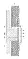
- FIG. 2 is an enlarged view of a portion surrounded by a circle in FIG. 1. It is sectional drawing of the other example of an optical transmission / reception module.
- FIG. 4 is an enlarged view of a portion surrounded by a circle in FIG. 3. It is sectional drawing of the optical transmission / reception module by 1st Embodiment.
- FIG. 6 is an enlarged view of a portion surrounded by a circle in FIG. 5.
- FIG. 6 is an enlarged plan view of a portion surrounded by a circle in FIG. 5. It is an expanded sectional view of a flexible substrate. It is sectional drawing of the optical transmission / reception module by 2nd Embodiment. It is an enlarged plan view which shows the vicinity of the part to which the flexible substrate was connected to the control board.
- Optical transceiver module 12 Housing 12a Fin 12b Heat receiving part 12c Top surface 14 Optical input / output device 16 Optical fiber 17 Optical connector 18 Control board 18a Wiring pattern 18b Heat radiation pad 18c Via 19 Through opening 20 Driver IC 20a Bottom electrode 22 Heat radiation sheet 32, 42 Flexible substrate 32a Coverlay 32b Conductive layer 32c Heat radiation pad 32d Via 34 Heat radiation adhesive
- FIG. 1 is a cross-sectional view of an optical module to which the present invention is applicable.
- FIG. 2 is an enlarged view of a portion surrounded by a circle in FIG.
- the optical module shown in FIG. An optical input / output device 14, an optical connector 17 for connecting an optical fiber 16 to the optical input / output device 14, and a control board 18 for controlling the optical input / output device 14 are provided in the housing 12 of the optical transceiver module 10. Is housed.
- the housing 12 is a mechanical component of the optical transceiver module 10 and is made of a metal material having good thermal conductivity such as an aluminum alloy, and is a metal housing.
- the control board 18 is a relatively rigid printed board (rigid board) formed of a material such as glass epoxy, and electronic components are mounted on both sides thereof.
- a driver IC which is a device for controlling or amplifying an electric signal for driving the optical input / output device 14, and an electric signal output from the optical input / output device 14
- the amplifier IC which is a device for amplifying the signal, handles a very high-speed signal, and therefore has a small signal amplitude.
- the driver IC and the amplifier IC are arranged as close to the optical input / output device 14 as possible. That is, in FIG. 1, the driver IC and the amplifier IC are arranged in a portion surrounded by a circle. In FIG. 1, it is assumed that an IC arranged in a circled portion is a driver IC 20.
- the driver IC 20 is a bottom electrode part having a bottom electrode 20a, and heat generated in the driver IC 20 is efficiently released from the bottom electrode 20a.
- a lead terminal 20 b extends from the side surface of the driver IC 20 and is soldered to the wiring pattern 18 a of the control board 18.
- the wiring pattern 18a often includes a ground pattern (GND pattern).
- the control board 18 is a multilayer printed board formed of a rigid board in which a conductive layer made of a metal such as copper and a base material made of an insulating material such as glass epoxy are laminated in multiple layers. is there.
- a heat radiating pad 18 b is formed at a portion facing the bottom electrode 20 a of the driver IC 20.
- the heat dissipation pad 18b is a solid pattern formed of the same material as the wiring pattern 18a, and is formed as a part of the wiring pattern 18a.
- a plurality of vias 18 c extend through the control board 18 to the opposite surface of the control board 18 from the heat dissipation pad 18 b.
- the driver IC 20 which is a bottom electrode component, is mounted on the control board 18 with the bottom electrode 20a facing the heat dissipating pad 18b.
- An adhesive heat radiation adhesive having a high heat transfer rate is filled between the bottom electrode 20a and the heat radiation pad 18b. Therefore, the heat generated in the driver IC 20 is transmitted from the heat dissipation pad 18b to the wiring pattern 18a as the GND pattern and released to the surroundings. At the same time, the heat generated in the driver IC 20 is transmitted from the heat radiating pad 18b to the opposite surface side of the control board 18 through the via 18c, and is released to the surroundings there.
- the heat from the driver IC 20 is transmitted to the control board 18, released from the control board 18 to the surrounding air, and the heat is transmitted to the housing 12. It is discharged to the outside of the housing 12 through the fins 12a of the housing 12 and the like. Therefore, the heat released from the driver IC 20 is first transmitted through the control board 18, then transferred to the air around the control board 18, and then transferred to the housing 12.
- the heat conductivity of air and the heat transfer coefficient between the air, the housing, and the control board are not so good, the heat dissipation efficiency can be improved if heat can be radiated without air.
- the heat receiving portion 12b which is a part of the housing 12, is connected to the opposite side of the portion of the control board 18 where the driver IC 20 is mounted via the heat dissipation sheet 22.
- the heat released from the driver IC 20 can be directly transmitted to the housing 12 without passing through air.
- the via 18c electrically connected to the bottom electrode 20a of the driver IC 20 extends to the opposite surface of the control board 18, the housing 12 and the driver IC 20 are in an electrically connected state. End up. For this reason, when static electricity of the housing 12 is discharged to the driver IC 20 through the via 18c, there is a possibility that an ESD problem may occur.
- the heat released from the driver IC 20 can be directly transmitted to the housing 12 without passing through air, and the housing 12 and the driver IC 20 are electrically insulated. I have to.
- FIG. 5 is a cross-sectional view of an optical transceiver module 30 which is an example of the optical module according to the first embodiment. 5, parts that are the same as the parts shown in FIG. 1 are given the same reference numerals, and descriptions thereof will be omitted.
- the housing 12 of the optical transmission / reception module 30 has a heat receiving part 12b as in the optical transmission / reception module 10A shown in FIG.
- the heat receiving portion 12b is not connected to the control board 18, but is connected to the flexible board 32 on which the driver IC 20 is mounted.
- the flexible board 32 is mounted on the control board 18 in a state where the driver IC 20 is mounted on the flexible board 32.
- the flexible substrate 32 only needs to be large enough to mount the driver IC 20.
- the flexible substrate has a first surface on which the driver IC is mounted and a second surface on the opposite side.
- a portion of the control board 18 where the flexible board 32 is mounted is provided with a through opening through which the heat receiving portion 12b of the housing 12 can enter. That is, the flexible substrate 32 on which the driver IC 20 is mounted is mounted so as to cover the through opening of the control substrate 18, and the second surface of the flexible substrate 32 is exposed in the through opening.
- the heat receiving portion 12b of the housing 12 can extend to the second surface of the flexible substrate 32 or the vicinity thereof by passing through the through opening. Therefore, the heat receiving portion 12b faces the driver IC 20 with the flexible substrate 32 interposed therebetween.
- FIG. 6 is an enlarged view of a portion surrounded by a circle in FIG.
- FIG. 7 is an enlarged plan view of a portion surrounded by a circle in FIG. 5 as viewed from the driver IC side.
- the flexible board 32 is mounted on the control board 18 so as to close the through opening 19 of the control board 18. Accordingly, the lead terminals of the driver IC 20 are first connected to the wiring pattern of the flexible board 32, and the wiring pattern of the flexible board 32 is connected to the wiring pattern of the control board 18 so that the driver IC 20 is mounted on the control board 18.
- a circuit equivalent to can be formed.
- the heat receiving portion 12 b of the housing 12 extends toward the flexible substrate 32 through the through opening 19 of the control substrate 18. Then, the flat top surface 12 c of the heat receiving portion 12 b is bonded to the flexible substrate 32 with a heat radiation adhesive 34.
- the heat radiation adhesive 34 is an adhesive made of a material having a high thermal conductivity, and is in close contact with the flat top surface 12c of the heat receiving portion 12b and the flexible substrate 32 so that the heat receiving portion 12ab can be easily transferred from the flexible substrate 32.
- the above-described through-opening 19 is not necessarily a through-hole provided in the control board 18, and may be a notch provided in an edge (side) of the control board 18. That is, when the mounting position of the driver IC 20 on the control board 18 is close to the edge (side) of the control board 18, not the through opening 19 but a cut cut into the inside of the control board 18 from the edge (side). It may be missing.
- the flexible substrate 32 has a structure in which a cover lay 32a and a conductive layer 32b serving as an insulating base material are laminated.
- the coverlay 32a is a polyimide layer, for example, and has electrical insulation.
- the bottom electrode 20 a of the driver IC 20 is bonded to the heat dissipation pad 32 c of the flexible substrate 32.
- a via 32 d extends from the heat dissipating pad 32 c into the flexible substrate 32.
- the via 32 d does not reach the outermost cover lay 32 a bonded by the heat radiation adhesive 34. Therefore, at least one layer of highly insulating coverlay 32 is interposed between the via 32 d electrically connected to the driver IC 20 and the heat receiving portion 12 b of the housing 12.
- the driver IC 20 and the housing 12 are electrically separated, and static electricity generated in the housing 12 is suppressed from flowing to the driver IC 20. That is, the ESD problem for the driver IC 20 is solved.
- the heat receiving portion 12b extending from the housing 12 that is the frame ground portion (FG) is connected to the control board 18 that is the signal ground portion (SG) by the cover lay 32a of the flexible substrate 32. It is electrically separated and insulated from the IC 20. Therefore, the heat from the driver IC 20 is partially absorbed by the housing 12 while the housing 12 that is the frame grounding portion (FG) and the control board 18 that is the signal grounding portion (SG) are electrically separated from each other.
- a heat dissipation structure that can be absorbed by a certain heat receiving portion 12b is realized.
- the cover lay 32a made of polyimide is extremely thin and has a thickness of about 10 ⁇ m, for example.
- the thermal conductivity of the polyimide itself is 0.2 W / mK, which is relatively small.
- the coverlay 32a is very thin, the thermal resistance can be sufficiently reduced.
- polyimide has a sufficient resistance to heat so as to be used for heat-resistant tape.
- the cover lay (polyimide layer) of the flexible substrate is used as a heat transfer path having electrical insulation rather than a simple insulator. Such a method of use has never existed before. In recent years, studies have been actively conducted on making polyimide-based materials have higher thermal conductivity, and it is expected that polyimide materials having higher thermal conductivity than those currently developed will be developed. If such a polyimide material is used as the coverlay 32a, the ESD resistance can be further improved.
- FIG. 9 is a cross-sectional view of an optical transceiver module 40 which is an example of an optical module according to the second embodiment. 9, parts that are the same as the parts shown in FIG. 1 are given the same reference numerals, and descriptions thereof will be omitted.
- FIG. 10 is an enlarged plan view showing the vicinity of a portion where the flexible board 42 in FIG. 9 is connected to the control board 18.
- a flexible board 42 is provided between the optical input / output device 14 and the control board 18, and the driver IC 20 is mounted on the flexible board 42. That is, the distance between the optical input / output device 14 and the control board 18 shown in FIG. 1 is increased, and the flexible board for electrically connecting the optical input / output device 14 and the control board 18 is extended to be a flexible board. 42. Therefore, the flexible board 32 on which the driver IC 20 is mounted is not mounted on the control board 18 as in the first embodiment, and instead, the flexible board 42 on which the driver IC 20 is mounted is connected to the control board 18. Therefore, the driver IC 20 is mounted on the upper surface of the flexible substrate 42 extending between the optical input / output device 14 and the control substrate 18.
- a heat receiving portion 12b is provided as a part of the housing 12 so as to protrude inward.
- the top surface 12c of the heat receiving portion 12b is a flat surface, and is bonded to the second surface of the flexible substrate 42 (on the opposite side of the first surface on which the driver IC 20 is mounted) by the heat radiation adhesive 34.
- the top surface 12c of the heat receiving portion 12b is larger than the driver IC 20, and is flexible so that the portion of the flexible substrate 42 on which the driver IC 20 is mounted is aligned with the portion of the flexible substrate 42 connected to the control board 18. The substrate 42 is supported.
- the portion of the flexible board 42 connected to the control board 18 is considered to be a bending prohibited area because there is a possibility that the connection is damaged when bending stress is applied, and measures are taken so that bending does not act.
- the flexible substrate 42 is maintained in a straight line (flat surface) by the top surface 12c of the heat receiving portion 12b, it is not necessary to take another measure that does not particularly cause bending.
- the heat receiving portion 12b is arranged directly below the driver IC 20. Therefore, the heat released from the bottom electrode of the driver IC 20 is directly transmitted to the housing 12 (without air) via the flexible substrate 42 and the heat radiation adhesive 34 and is released from the housing 12 to the outside.
- the heat dissipation efficiency of the driver IC 20 is improved.
- the flexible substrate 42 has the same configuration as the flexible substrate 32 shown in FIG. 8, and the driver IC 20 and the housing 12 are electrically separated by the cover lay of the flexible substrate 42. Therefore, as described in the flexible substrate 32, static electricity generated in the housing 12 is suppressed from flowing to the driver IC 20, and the ESD problem for the driver IC 20 is solved.
- the heat transfer coefficient between the flexible boards 32 and 42 and the housing 12 is obtained by bringing the flexible boards 32 and 42 into close contact with the top surface 12c of the heat receiving portion 12b with the heat radiation adhesive 34. Is increasing. In this way, since the heat transfer path can be shortened by bonding, sufficient heat dissipation can be achieved even if the thermal conductivity is relatively small, such as a silicon-based heat radiation adhesive (thermal conductivity: about 3 W / mK). Can be realized. In addition, since the mechanical strength is increased, the flexible substrate can be fixed so as not to bend.
- a heat-dissipating sheet may be sandwiched between the flexible substrates 32 and 42 and the top surface 12c of the heat receiving portion 12b.
- a graphite sheet can be used as the sheet having heat dissipation properties. Simply sandwiching the sheet may cause a gap between the sheet and the flexible substrate 32, 42 or the top surface 12c of the heat receiving portion 12b. Therefore, an adhesive may be attached to the graphite sheet, and the graphite sheet may be attached to the flexible substrates 32 and 42 and the top surface 12c of the heat receiving portion 12b. Or it is good also as using the heat dissipation sheet which itself has adhesiveness like a silicon heat dissipation sheet.
- an elastic silicon heat radiating sheet may be sandwiched between the flexible substrates 32 and 42 and the top surface 12c of the heat receiving portion 12b.
- the flexible substrates 32 and 42 are not fixed to the top surface 12c of the heat receiving portion 12b with an adhesive or an adhesive, there is an advantage that it is easy to disassemble at the time of repair or the like.
- the flexible substrates 32 and 42 are parts that must be removed when the optical module is disassembled, it is effective to use a silicon heat dissipation sheet having elasticity.
- the heat receiving portion 12b of the housing 12 is used as a heat radiating member (heat sink) to absorb heat from the driver IC 20 and release it to the outside.
- the part 12b) does not necessarily have to be part of the housing 12.
- the heat radiating member (heat receiving portion 12 b) may be created separately from the housing 12 and connected to the housing 12. Alternatively, if there is a mechanism component that easily radiates heat other than the housing 12, the heat dissipation member may be connected to the mechanism component.
- the present invention is applicable to an optical module.
Landscapes
- Engineering & Computer Science (AREA)
- Microelectronics & Electronic Packaging (AREA)
- Physics & Mathematics (AREA)
- Thermal Sciences (AREA)
- General Physics & Mathematics (AREA)
- Optics & Photonics (AREA)
- Cooling Or The Like Of Electrical Apparatus (AREA)
- Optical Couplings Of Light Guides (AREA)
Abstract
La présente invention concerne un module optique comportant un premier substrat souple présentant une première surface, sur laquelle un composant est monté, et une seconde surface sur le côté opposé à la première surface. Un composant d'électrode de surface inférieure comprenant une électrode de dissipation thermique sur la face inférieure est monté sur la première surface du substrat souple. Un élément de dissipation thermique pour l'absorption de la chaleur provenant du composant d'électrode de surface inférieure et l'évacuation de la chaleur vers l'extérieur est disposé à proximité de la seconde surface du substrat souple dans la position dans laquelle le composant d'électrode de surface inférieure est monté.
Priority Applications (4)
| Application Number | Priority Date | Filing Date | Title |
|---|---|---|---|
| JP2011519331A JP5218657B2 (ja) | 2009-06-15 | 2009-06-15 | 光モジュール |
| PCT/JP2009/060888 WO2010146652A1 (fr) | 2009-06-15 | 2009-06-15 | Module optique |
| US13/325,817 US20120082420A1 (en) | 2009-06-15 | 2011-12-14 | Optical module |
| US14/299,655 US9507108B2 (en) | 2009-06-15 | 2014-06-09 | Optical module |
Applications Claiming Priority (1)
| Application Number | Priority Date | Filing Date | Title |
|---|---|---|---|
| PCT/JP2009/060888 WO2010146652A1 (fr) | 2009-06-15 | 2009-06-15 | Module optique |
Related Child Applications (1)
| Application Number | Title | Priority Date | Filing Date |
|---|---|---|---|
| US13/325,817 Continuation US20120082420A1 (en) | 2009-06-15 | 2011-12-14 | Optical module |
Publications (1)
| Publication Number | Publication Date |
|---|---|
| WO2010146652A1 true WO2010146652A1 (fr) | 2010-12-23 |
Family
ID=43355991
Family Applications (1)
| Application Number | Title | Priority Date | Filing Date |
|---|---|---|---|
| PCT/JP2009/060888 Ceased WO2010146652A1 (fr) | 2009-06-15 | 2009-06-15 | Module optique |
Country Status (3)
| Country | Link |
|---|---|
| US (2) | US20120082420A1 (fr) |
| JP (1) | JP5218657B2 (fr) |
| WO (1) | WO2010146652A1 (fr) |
Cited By (1)
| Publication number | Priority date | Publication date | Assignee | Title |
|---|---|---|---|---|
| CN104238042A (zh) * | 2013-06-13 | 2014-12-24 | 梅兰诺克斯科技有限公司 | 用于光电互连模块的集成光冷却芯 |
Families Citing this family (13)
| Publication number | Priority date | Publication date | Assignee | Title |
|---|---|---|---|---|
| US20150003839A1 (en) * | 2012-01-13 | 2015-01-01 | Yuuji Minota | Optical transceiver |
| US9063305B2 (en) * | 2012-11-26 | 2015-06-23 | Avago Technologies General Ip (Singapore) Pte. Ltd. | Methods and systems for dissipating heat in optical communications modules |
| FR2999864A1 (fr) * | 2012-12-19 | 2014-06-20 | Valeo Systemes Thermiques | Dispositif de refroidissement pour carte de circuit imprime |
| US9170386B2 (en) * | 2013-04-08 | 2015-10-27 | Hon Hai Precision Industry Co., Ltd. | Opto-electronic device assembly |
| US9250027B2 (en) | 2013-05-01 | 2016-02-02 | Finisar Corporation | Thermal management structures for optoelectronic systems |
| US10534147B2 (en) * | 2014-06-27 | 2020-01-14 | Mitsubishi Electric Corporation | Optical transceiver |
| US20160274321A1 (en) * | 2015-03-21 | 2016-09-22 | Ii-Vi Incorporated | Flexible Structured Optical Modules |
| JP6237706B2 (ja) * | 2015-06-05 | 2017-11-29 | 富士通オプティカルコンポーネンツ株式会社 | 光モジュール及び光送受信装置 |
| FI3121630T3 (fi) * | 2015-07-21 | 2023-06-29 | Tyco Electronics Svenska Holdings Ab | Lämmönhallinnaltaan parannettu optoelektroninen moduuli |
| CN111432110B (zh) | 2015-11-23 | 2022-08-16 | 深圳市大疆创新科技有限公司 | 影像撷取模组及航拍飞行器 |
| US10993352B2 (en) * | 2019-01-08 | 2021-04-27 | Te Connectivity Corporation | Thermal transfer device for a pluggable module assembly |
| JP2022049327A (ja) * | 2020-09-16 | 2022-03-29 | キオクシア株式会社 | 半導体記憶装置 |
| CN114488423A (zh) * | 2020-10-27 | 2022-05-13 | 青岛海信宽带多媒体技术有限公司 | 一种光模块 |
Citations (5)
| Publication number | Priority date | Publication date | Assignee | Title |
|---|---|---|---|---|
| JPH09102688A (ja) * | 1995-10-06 | 1997-04-15 | Hitachi Ltd | 電子パッケージの実装構造およびそれを用いたノートブック型コンピュータ |
| JP2003115681A (ja) * | 2001-10-04 | 2003-04-18 | Denso Corp | 電子部品の実装構造 |
| JP2004140171A (ja) * | 2002-10-17 | 2004-05-13 | Denso Corp | 多層プリント基板、多層プリント基板の放熱構造および多層プリント基板の製造方法 |
| JP2005005629A (ja) * | 2003-06-16 | 2005-01-06 | Hitachi Ltd | 電子装置 |
| JP2006294754A (ja) * | 2005-04-07 | 2006-10-26 | Denso Corp | 電子装置の放熱構造 |
Family Cites Families (20)
| Publication number | Priority date | Publication date | Assignee | Title |
|---|---|---|---|---|
| JPH1140901A (ja) * | 1997-07-23 | 1999-02-12 | Sharp Corp | 回路基板 |
| JPH11345987A (ja) | 1998-06-02 | 1999-12-14 | Sony Corp | 光リンク用送受信モジュール実装方法及びそのリジッド・フレキシブル基板 |
| US6340796B1 (en) * | 1999-06-02 | 2002-01-22 | Northrop Grumman Corporation | Printed wiring board structure with integral metal matrix composite core |
| US6605778B2 (en) * | 2000-10-02 | 2003-08-12 | Siemens Aktiengesellschaft | Circuit carrier, in particular printed circuit board |
| DE60222815T2 (de) * | 2001-04-03 | 2008-07-03 | AUTONETWORKS Technologies, LTD., Yokkaichi | Optischer Stecker, Halterungsvorrichtung für optisches Element und Montageteil für einen optischen Stecker |
| US6744135B2 (en) * | 2001-05-22 | 2004-06-01 | Hitachi, Ltd. | Electronic apparatus |
| JP4015497B2 (ja) * | 2002-07-30 | 2007-11-28 | 日本オプネクスト株式会社 | 光通信器 |
| JP2004087594A (ja) | 2002-08-23 | 2004-03-18 | Alps Electric Co Ltd | 電子回路ユニットの放熱構造 |
| US7070341B2 (en) * | 2002-10-02 | 2006-07-04 | Emcore Corporation | High-density fiber-optic module with multi-fold flexible circuit |
| JP2004172459A (ja) * | 2002-11-21 | 2004-06-17 | Advics:Kk | 電子制御装置における電子部品の放熱構造 |
| JP4186732B2 (ja) * | 2003-07-24 | 2008-11-26 | 株式会社村田製作所 | 電子機器 |
| JP4037815B2 (ja) * | 2003-09-29 | 2008-01-23 | オムロンレーザーフロント株式会社 | レーザダイオードモジュール、レーザ装置、及びレーザ加工装置 |
| US7271461B2 (en) * | 2004-02-27 | 2007-09-18 | Banpil Photonics | Stackable optoelectronics chip-to-chip interconnects and method of manufacturing |
| US7033927B2 (en) * | 2004-06-22 | 2006-04-25 | International Business Machines Corporation | Apparatus and method for thermal isolation, circuit cooling and electromagnetic shielding of a wafer |
| JP4395036B2 (ja) | 2004-09-17 | 2010-01-06 | 富士通株式会社 | 光モジュール |
| JP4556174B2 (ja) * | 2004-12-15 | 2010-10-06 | 日本電気株式会社 | 携帯端末機器及び放熱方法 |
| US7764462B1 (en) * | 2006-01-13 | 2010-07-27 | Marvell International Ltd. | Thermal solution for drive systems such as hard disk drives and digital versatile discs |
| JP2007294619A (ja) | 2006-04-24 | 2007-11-08 | Nec Saitama Ltd | 放熱構造 |
| JP2008010552A (ja) * | 2006-06-28 | 2008-01-17 | Nec Electronics Corp | パワーアンプモジュール |
| US7808788B2 (en) * | 2007-06-29 | 2010-10-05 | Delphi Technologies, Inc. | Multi-layer electrically isolated thermal conduction structure for a circuit board assembly |
-
2009
- 2009-06-15 WO PCT/JP2009/060888 patent/WO2010146652A1/fr not_active Ceased
- 2009-06-15 JP JP2011519331A patent/JP5218657B2/ja not_active Expired - Fee Related
-
2011
- 2011-12-14 US US13/325,817 patent/US20120082420A1/en not_active Abandoned
-
2014
- 2014-06-09 US US14/299,655 patent/US9507108B2/en not_active Expired - Fee Related
Patent Citations (5)
| Publication number | Priority date | Publication date | Assignee | Title |
|---|---|---|---|---|
| JPH09102688A (ja) * | 1995-10-06 | 1997-04-15 | Hitachi Ltd | 電子パッケージの実装構造およびそれを用いたノートブック型コンピュータ |
| JP2003115681A (ja) * | 2001-10-04 | 2003-04-18 | Denso Corp | 電子部品の実装構造 |
| JP2004140171A (ja) * | 2002-10-17 | 2004-05-13 | Denso Corp | 多層プリント基板、多層プリント基板の放熱構造および多層プリント基板の製造方法 |
| JP2005005629A (ja) * | 2003-06-16 | 2005-01-06 | Hitachi Ltd | 電子装置 |
| JP2006294754A (ja) * | 2005-04-07 | 2006-10-26 | Denso Corp | 電子装置の放熱構造 |
Cited By (2)
| Publication number | Priority date | Publication date | Assignee | Title |
|---|---|---|---|---|
| CN104238042A (zh) * | 2013-06-13 | 2014-12-24 | 梅兰诺克斯科技有限公司 | 用于光电互连模块的集成光冷却芯 |
| CN104238042B (zh) * | 2013-06-13 | 2017-08-08 | 迈络思科技有限公司 | 用于光电互连模块的集成光冷却芯 |
Also Published As
| Publication number | Publication date |
|---|---|
| JP5218657B2 (ja) | 2013-06-26 |
| US9507108B2 (en) | 2016-11-29 |
| US20140286614A1 (en) | 2014-09-25 |
| US20120082420A1 (en) | 2012-04-05 |
| JPWO2010146652A1 (ja) | 2012-11-29 |
Similar Documents
| Publication | Publication Date | Title |
|---|---|---|
| JP5218657B2 (ja) | 光モジュール | |
| KR101044200B1 (ko) | 리지드-플렉서블 회로기판 및 그 제조방법 | |
| US7872869B2 (en) | Electronic chip module | |
| CN101958314B (zh) | 对叠式系统级封装及其制造和使用方法 | |
| JP5413971B2 (ja) | 電子部品実装装置及びその製造方法 | |
| US11984380B2 (en) | Semiconductor package, semiconductor device, semiconductor package-mounted apparatus, and semiconductor device-mounted apparatus | |
| CN116577885B (zh) | 一种光模块封装结构 | |
| JP2009016626A (ja) | 半導体モジュール装置および半導体モジュール装置の製造方法ならびにフラットパネル型表示装置,プラズマディスプレイパネル | |
| JP2011108924A (ja) | 熱伝導基板及びその電子部品実装方法 | |
| WO2017022221A1 (fr) | Structure de dissipation de chaleur et appareil électronique | |
| JPH11233904A (ja) | 放熱構造プリント基板 | |
| CN211267229U (zh) | 电子设备 | |
| US9621196B2 (en) | High-frequency module and microwave transceiver | |
| CN108293295A (zh) | 用于发热电子部件的承载和散热的电子部件载体 | |
| JP2005026263A (ja) | 混成集積回路 | |
| JP2005311230A (ja) | 回路モジュールおよびこの回路モジュールを用いた回路装置 | |
| JP2006093546A (ja) | 放熱シート、放熱筒状体およびそれらを用いた放熱構造 | |
| JP2011029504A (ja) | 実装構造体 | |
| JP2010267954A (ja) | 電子機器 | |
| KR20150076816A (ko) | 전자 부품 모듈 | |
| KR20200141321A (ko) | 방열 칩 온 필름 패키지 | |
| JP2020191316A (ja) | 回路モジュール | |
| JP2019153611A (ja) | モジュール | |
| JP2004111633A (ja) | 光通信器 | |
| WO2010131578A1 (fr) | Dispositif à semi-conducteurs doté d'un périphérique d'entrée et de sortie de signal optique incorporé et dispositif électronique équipé dudit dispositif |
Legal Events
| Date | Code | Title | Description |
|---|---|---|---|
| 121 | Ep: the epo has been informed by wipo that ep was designated in this application |
Ref document number: 09846145 Country of ref document: EP Kind code of ref document: A1 |
|
| WWE | Wipo information: entry into national phase |
Ref document number: 2011519331 Country of ref document: JP |
|
| NENP | Non-entry into the national phase |
Ref country code: DE |
|
| 122 | Ep: pct application non-entry in european phase |
Ref document number: 09846145 Country of ref document: EP Kind code of ref document: A1 |