WO2010146665A1 - Dispositif de communication optique et procédé de commande économe en énergie pour un dispositif de communication optique - Google Patents
Dispositif de communication optique et procédé de commande économe en énergie pour un dispositif de communication optique Download PDFInfo
- Publication number
- WO2010146665A1 WO2010146665A1 PCT/JP2009/060962 JP2009060962W WO2010146665A1 WO 2010146665 A1 WO2010146665 A1 WO 2010146665A1 JP 2009060962 W JP2009060962 W JP 2009060962W WO 2010146665 A1 WO2010146665 A1 WO 2010146665A1
- Authority
- WO
- WIPO (PCT)
- Prior art keywords
- packet
- unit
- power saving
- signal
- mode flag
- Prior art date
- Legal status (The legal status is an assumption and is not a legal conclusion. Google has not performed a legal analysis and makes no representation as to the accuracy of the status listed.)
- Ceased
Links
Images











Classifications
-
- H—ELECTRICITY
- H04—ELECTRIC COMMUNICATION TECHNIQUE
- H04L—TRANSMISSION OF DIGITAL INFORMATION, e.g. TELEGRAPHIC COMMUNICATION
- H04L12/00—Data switching networks
- H04L12/28—Data switching networks characterised by path configuration, e.g. LAN [Local Area Networks] or WAN [Wide Area Networks]
- H04L12/2854—Wide area networks, e.g. public data networks
- H04L12/2856—Access arrangements, e.g. Internet access
- H04L12/2869—Operational details of access network equipments
- H04L12/287—Remote access server, e.g. BRAS
-
- H—ELECTRICITY
- H04—ELECTRIC COMMUNICATION TECHNIQUE
- H04L—TRANSMISSION OF DIGITAL INFORMATION, e.g. TELEGRAPHIC COMMUNICATION
- H04L12/00—Data switching networks
- H04L12/28—Data switching networks characterised by path configuration, e.g. LAN [Local Area Networks] or WAN [Wide Area Networks]
- H04L12/2854—Wide area networks, e.g. public data networks
- H04L12/2856—Access arrangements, e.g. Internet access
- H04L12/2858—Access network architectures
- H04L12/2861—Point-to-multipoint connection from the data network to the subscribers
-
- H—ELECTRICITY
- H04—ELECTRIC COMMUNICATION TECHNIQUE
- H04L—TRANSMISSION OF DIGITAL INFORMATION, e.g. TELEGRAPHIC COMMUNICATION
- H04L12/00—Data switching networks
- H04L12/28—Data switching networks characterised by path configuration, e.g. LAN [Local Area Networks] or WAN [Wide Area Networks]
- H04L12/2854—Wide area networks, e.g. public data networks
- H04L12/2856—Access arrangements, e.g. Internet access
- H04L12/2869—Operational details of access network equipments
- H04L12/2878—Access multiplexer, e.g. DSLAM
- H04L12/2879—Access multiplexer, e.g. DSLAM characterised by the network type on the uplink side, i.e. towards the service provider network
- H04L12/2885—Arrangements interfacing with optical systems
-
- H—ELECTRICITY
- H04—ELECTRIC COMMUNICATION TECHNIQUE
- H04Q—SELECTING
- H04Q11/00—Selecting arrangements for multiplex systems
- H04Q11/0001—Selecting arrangements for multiplex systems using optical switching
- H04Q11/0062—Network aspects
- H04Q11/0067—Provisions for optical access or distribution networks, e.g. Gigabit Ethernet Passive Optical Network (GE-PON), ATM-based Passive Optical Network (A-PON), PON-Ring
-
- H—ELECTRICITY
- H04—ELECTRIC COMMUNICATION TECHNIQUE
- H04Q—SELECTING
- H04Q11/00—Selecting arrangements for multiplex systems
- H04Q11/0001—Selecting arrangements for multiplex systems using optical switching
- H04Q11/0062—Network aspects
- H04Q2011/0079—Operation or maintenance aspects
-
- H—ELECTRICITY
- H04—ELECTRIC COMMUNICATION TECHNIQUE
- H04Q—SELECTING
- H04Q11/00—Selecting arrangements for multiplex systems
- H04Q11/0001—Selecting arrangements for multiplex systems using optical switching
- H04Q11/0062—Network aspects
- H04Q2011/0088—Signalling aspects
Definitions
- the disclosed technology relates to an optical communication device and a power saving control method for the optical communication device.
- the OLT (Optical Line Terminal) device which is a terminal device for a carrier (carrier), and the ONT (Optical Network Terminal, ONU, which is a terminal device for an end user (communication business subscriber), are used.
- a branching device called a star coupler for branching one input light to many outputs in the middle of the optical fiber network including the device, and branching one optical fiber from the OLT to There is a communication system called PON (Passive Optical Network) that connects to ONT.
- PON Passive Optical Network
- PON Passive Double Star
- a termination device for example, by recognizing that it is a packet containing a control signal for turning on / off the power of its own device instead of communication from another communication device by the header portion of the received packet, There has been proposed a communication device that recognizes the control contents received by the own device by the control signal.
- a frame packet signal having a packet overhead portion corresponding to the transmission speed of the slave communication device and frame synchronization information for establishing frame synchronization is transferred from the main communication device to one packet signal length or
- a communication system in which a packet is divided into a plurality of packet time lengths and transmitted at intervals of frame periods.
- the subordinate communication device receives a frame packet signal that matches the transmission rate of its own device from one packet signal length or a plurality of frame packet signals divided within one packet time length, and receives frame synchronization information. Establish frame synchronization by reading
- the communication device in a communication network including a communication device as a termination device, the communication device must always be turned on in preparation for communication even in an idle state in which communication is not performed.
- the main communication device such as the OLT has a large power consumption because it must establish communication with a plurality of subordinate communication devices such as the ONT.
- the disclosed technology has been made to solve the above problems (issues), and from the viewpoint of energy saving, an optical communication device that suppresses power consumption during operation of a communication device, particularly a main communication device such as an OLT. And it aims at providing the power-saving control method of an optical communication apparatus.
- the disclosed technique is applied to a subscriber-side optical communication apparatus in an optical communication system that is connected to a plurality of subscriber-side optical communication apparatuses and performs bidirectional communication.
- the presence / absence of a packet transmitted from the person side optical communication device is monitored, the power saving mode flag of the own device is generated based on the presence / absence of the monitored packet, and the power saving control of the own device is performed based on the generated power saving mode flag. Is a requirement.
- the power supply of the main termination device is always turned on. Except when it is turned on and the delay time is measured, it is possible to control the power on / off of the main termination device according to the presence / absence of packet transmission / reception. Therefore, it is possible to save power, reduce the amount of heat generation, and improve the integration degree of the main termination device.
- FIG. 1 is a block diagram showing the configuration of the PON system.
- FIG. 2 is a sequence diagram showing a ranging processing procedure.
- FIG. 3 is a diagram for explaining a frame configuration and a packet configuration of an upstream signal from the ONT device to the OLT device.
- FIG. 4 is a diagram illustrating a sparsely mounted state in which a few ONT devices are operating among a plurality of ONT devices, and there are many non-operating ONT devices.
- FIG. 5A is a diagram illustrating a conventional packet configuration based on the number of branches.
- FIG. 5B is a diagram illustrating a packet configuration based on the number of branches in recent years.
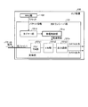
- FIG. 6 is a block diagram illustrating a configuration of the OLT device.
- FIG. 1 is a block diagram showing the configuration of the PON system.
- FIG. 2 is a sequence diagram showing a ranging processing procedure.
- FIG. 3 is a diagram for explaining a frame configuration and a packet configuration of an
- FIG. 7 is a diagram illustrating an outline in which ranging information having a fixed periodicity is included in the delay measurement window.
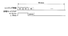
- FIG. 8 is a diagram illustrating an outline in which ranging information increases and the periodicity of the ranging information changes when end users dynamically increase.
- FIG. 9 is a diagram illustrating an outline in which ranging information decreases and the periodicity of ranging information changes when end users dynamically decrease.
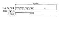
- FIG. 10 is a diagram illustrating an overview in which the periodicity of the static power saving mode flag is impaired, and the ranging information and the state of the power saving mode flag are inconsistent.
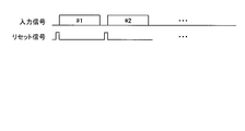
- FIG. 11 is a diagram illustrating an outline of a configuration example using a reset signal input from the MAC unit 102 to the optical transceiver unit 101.
- FIG. 12 is a diagram illustrating a configuration example in which the power is turned on / off using a timer unit having a reset signal and a timer function.
- FIG. 13 is a time chart when the timer unit turns off the power of the receiving unit.
- FIG. 14 is a block diagram illustrating the configuration of the OLT device according to the embodiment.
- FIG. 15 is a diagram illustrating a detailed configuration of the power saving mode flag generation unit.
- FIG. 16A is a diagram of a circuit example of the delay unit.
- FIG. 16B is a time chart illustrating signal states at respective points of the delay unit circuit.
- FIG. 17 is a diagram illustrating a circuit example of the latch circuit unit.
- FIG. 18 is a diagram illustrating an optical transceiver unit 101A including a packet monitoring unit.
- FIG. 19 is a diagram illustrating a circuit example of the signal disconnection detection unit.
- FIG. 20 is a diagram illustrating a circuit example of the PD / TIA unit.
- FIG. 21 is a diagram illustrating a circuit example of the LIM unit.
- FIG. 22 is a diagram illustrating a circuit example of the output unit.
- FIG. 23 is a diagram illustrating a detailed configuration of the power saving control unit.
- FIG. 24 is a block diagram illustrating a configuration of an OLT device according to an application example.
- FIG. 25 is a block diagram illustrating a detailed configuration of the light intensity detection unit according to the application example.
- FIG. 26 is a time chart illustrating the power saving control process according to the embodiment and the application example.
- FIG. 1 is a block diagram showing the configuration of the PON system.
- the OLT device 100 transmits a continuous signal in the ⁇ 1 band as a downstream signal to the ONT device 200ai via the star coupler SC.
- Each ONT device 200ai receives a continuous signal from the OLT device 100.
- each ONT device ai transmits a burst signal of ⁇ 2 band as an upstream signal to the OLT device 100 via the star coupler SC.
- Communication using a burst signal in the ⁇ 2 band varies in transmission distance and transmission path loss depending on the installation conditions of each ONT device 200ai. For this reason, the OLT device 100 performs time division multiplexing control so that burst signals output from the ONT devices 200ai do not collide with each other.
- optical communication is performed between the optical transceiver unit 101 of the OLT device 100 and the optical transceiver unit 201Ai of the ONT device 200ai.
- the optical transceiver unit 101 and the optical transceiver unit 201Ai are modules that are controlled by a MAC LSI (Media Access Control Large Scale Integration) and perform optical communication.
- MAC LSI Media Access Control Large Scale Integration
- a communication delay measurement is performed in order to communicate between the OLT and the ONT when a line is laid when an end user joins. It is carried out.
- the communication delay measurement is called “ranging” and is a function controlled by a MAC LSI generally mounted in the OLT apparatus 100.
- FIG. 2 is a sequence diagram showing a ranging processing procedure.
- the ONT device 200ai is activated.
- the ONT device 200ai transmits a frame signal to the OLT device 100 in order to achieve frame synchronization with the OLT device 100.
- step S13 the OLT device 100 that has received the frame signal from the ONT device 200ai transmits a registration request transmission permission signal to the OLT device 100 to the unregistered ONT device 200ai.
- step S ⁇ b> 14 the ONT device 200 ai transmits a registration request to the OLT device 100 so as to register itself with the OLT device 100.
- step S15 the OLT device 100 transmits the registration request transmission permission signal to the ONT device 200ai in step S13, and then receives the registration request from the ONT device 200ai in step S14.
- the distance between the devices 200ai is calculated.
- step S16 the OLT device 100 assigns an LL ID (Logical Link ID) to the ONT device 200ai that has transmitted the registration request received in step S14.
- the LL ID is an ID for uniquely identifying each ONT device 200ai in the PON system S.
- step S17 the OLT device 100 transmits a registration notification including the LL ID assigned in step S16 to the ONT device 200ai that has transmitted the registration request in step S14.
- step S18 the ONT device 200ai that has received the registration notification in step S17 transmits a registration notification confirmation indicating that the registration notification has been received to the OLT device 100.
- the OLT device 100 receives the registration notification confirmation, a series of registration processing of the ONT device 200ai is completed.
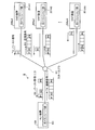
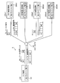
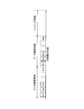
- FIG. 3 is a diagram for explaining a frame configuration and a packet configuration of an uplink signal from the ONT device 200ai to the OLT device 100.
- the frame of the uplink signal has a frame length with a transmission time of 1 [ms], for example.
- the frame of the uplink signal includes a data communication area for transmitting a packet from each end user and a ranging area used during ranging. Further, each packet having a packet length of 60 bytes included in the data communication area includes an overhead portion and a payload portion. Packets included in the data communication area are also referred to as PDS cells.
- the overhead part contains packet identification information, and the payload part contains user data.
- the overhead portion of 7 bytes in total includes “G”, “PR”, “DL”, and “DI” represented in FIG. “G” is a guard interval, which is a redundant part added for the purpose of preventing interference between packets.
- PR is a preamble, and includes a signal for causing the OLT device 100 to recognize the start of transmission of an upstream packet and giving timing for synchronization.
- DL is a delimiter and is information indicating the start position of the packet.
- DI is a data identifier and is identification information indicating the type of packet.
- the ranging area is, for example, a frame length with a transmission time of 1 [us].
- the ranging area includes one PDS-OAM (Operation Administration and Maintenance) packet called a delay measurement window for each ONT 200ai when there is a delay measurement instruction from the OLT device 100. Ranging is performed in this ranging area, and the time difference between the transmission timing of the registration request transmission permission signal transmitted from the OLT device 100 to each ONT device 200ai and the reception timing of the registration request that is a ranging packet from the ONT device 200ai is calculated. Measured as delay time.
- the ONT device 200ai can easily realize power saving by a combination of known technologies.
- the ONT devices 200ai are independent of each other, and in order to transmit a burst signal to the OLT device 100, a sleep mode (power saving mode) in which the circuit block is turned off except during transmission is obtained. It is easy to reduce power consumption.
- the OLT device 100 has a small number of ONT devices 200ai operating at the beginning of the service, and a small amount of data to be received. As shown in FIG. 4, this state is referred to as a sparsely mounted state in which a few ONT devices 200ai are operating among a plurality of ONT devices 200ai and a large number of inactive ONT devices 200ai exist.
- the number of branches by the star coupler SC is mainly 16 branches or 32 branches. For this reason, even if the sleep mode can be realized in the sparsely mounted state, the ratio of the sleep mode time to the delay measurement window in the ranging area is small. That is, even if the sleep mode time is secured, the number of delay measurement windows is small, so that the sleep mode time that can be secured in total is short. For this reason, when receiving a burst signal, the merit of shifting to the sleep mode is low.
- the packet transmission in the delay measurement window obtained from the ranging information from the MAC LSI is transmitted.
- a method of controlling the active mode (non-power saving mode) and the sleep mode of the OLT device 100 using the periodicity of the timing information is conceivable.
- FIG. 6 is a block diagram showing a configuration of the OLT device 100.
- the OLT device 100 includes an optical transceiver unit 101 and a MAC unit 102 that is a MAC LSI.
- the MAC unit 102 controls the PON system S.
- the MAC unit 102 recognizes a plurality of ONT devices 200ai, and performs packet transmission delay measurement when laying a line with each ONT device 200ai in order to communicate with the OLT device 100.
- Delay measurement is performed by a general function of the OLT device 100 called ranging as described above.
- packet transmission timing information (hereinafter also referred to as ranging information) from each ONT device 200ai can be obtained.
- the packet transmission timing information is information defining timing for transmitting a packet to the ONT device 200ai in consideration of a periodic delay time obtained by delay measurement.
- the optical transceiver unit 101 includes a power saving control unit 101a, a receiving unit 101b, and a packet information storage unit 101c.
- the packet information storage unit 101c acquires and stores periodic packet transmission timing information from the above-described packet transmission timing information. Then, a periodic power saving mode flag (a flag for identifying the active mode and the sleep mode) is generated from the stored transmission timing information, and is output to the power saving control unit 101a.
- the optical transceiver unit 101 acquires packet transmission timing information from the MAC unit 102 by low-speed serial communication of I2C (Inter-Integrated Circuit, SFP specification: 100 kbps).
- I2C Inter-Integrated Circuit, SFP specification: 100 kbps
- the power saving control unit 101a controls the power supply of the receiving unit 101b of the optical transceiver unit 101 in accordance with the periodic power saving mode flag input from the packet information storage unit 101c. Thereby, in the idling state where there is no reception packet and no transmission packet, the power of the reception unit 101b can be turned off to save power.
- the receiving unit 101b includes a PD (Photo Diode) / TIA (Trans Impedance amplifier) unit 101b1, a LIM (LIMiter amplifier) unit 101b2, and an output unit 101b3.
- the PD / TIA unit 101b1 converts a packet from an optical signal to an electrical signal by the photoelectric conversion element PD. Then, the PD / TIA unit 101b1 converts the electric signal from current to voltage by the current-voltage conversion element TIA and amplifies it.
- the PD / TIA unit 101b1 outputs the amplified voltage signal to the LIM unit 101b2.
- the LIM unit 101b2 removes over-input and amplification noise of the voltage signal input from the PD / TIA unit 101b1, and outputs it to the output unit 101b3.
- the output unit 101b3 demultiplexes a frame in which packets from a plurality of ONT devices 200ai are multiplexed into packets for each ONT device 200ai, and transmits each packet to, for example, an Ethernet (registered trademark) network.
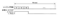
- ranging information having a fixed periodicity is included in the delay measurement window.
- This ranging information is not changed once stored in the packet information storage unit 101c. Therefore, a power saving mode flag (H: active mode, L: sleep mode) having a fixed periodicity is generated based on the fixed ranging information. That is, as long as the ranging information is not changed, the power saving of the receiving unit 101b can be controlled by a static power saving mode flag having a fixed periodicity.
- H active mode
- L sleep mode
- the power saving mode flag also needs to be changed in periodicity. That is, when the number of ONT devices 200ai increases, it is necessary to extend the period in which the power saving mode flag becomes “H” by the increment (# 7 ranging information). Further, when the ONT device 200ai decreases, the cycle in which the power saving mode flag becomes “H” must be shortened by the decrease (# 5 ranging information).
- the periodicity of the ranging information is not changed because it is fixedly stored in the packet information storage unit 101c. That is, as shown in FIG. 10, the periodicity of the static power saving mode flag is impaired, and the ranging information and the state of the power saving mode flag become inconsistent.
- the ONT device 200ai is added, the corresponding ranging information is left-justified. For example, according to FIG. 8, when # 7 ranging information is added after # 5 ranging information, # 7 is set next to # 5 without leaving # 6 ranging information area.
- periodic packet transmission timing information is not stored in the optical transceiver unit 101, but packet transmission timing information from the MAC unit 102 is used directly, that is, ranging information is updated for each packet. It is possible. However, since the I2C communication method used between the MAC unit 102 and the optical transceiver unit 101 is low speed, it is impossible to follow the increase / decrease in the ranging information in real time.
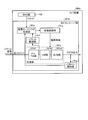
- the MAC unit 102 inputs the optical transceiver unit 101 to the optical transceiver unit 101 for the purpose of initializing the ATC (Auto Threshold Control) of the optical transceiver unit 101 immediately before the packet is input. It is conceivable to use a reset signal. For example, as shown in FIG. 12, a configuration in which the power is turned on and off using a timer unit 101d having a reset signal and a timer function is conceivable.
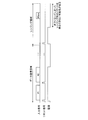
- the frame is divided into a data area and a ranging area as shown in FIG. Since the data packet is input immediately after the reset in the data communication area, there is no problem even if the receiving unit 101b is turned off when there is no reset. However, in the ranging area, it is unclear at what timing the ranging packet is transmitted, and therefore the receiving unit 101b must always be turned on. In the configuration of the OLT device 100 shown in FIG. 12, the power may be turned off during ranging, and there is a possibility that packets during ranging cannot be detected.
- the timer unit 101d measures a predetermined time from the input of the reset signal, and when there is no new reset signal input within the predetermined time, the power saving control unit 101a Turn off the power.
- the transmission timing of the ranging packet is unknown in the ranging area. For this reason, as shown in FIG. 13, when the power of the receiving unit 101b is already turned off at the timing when the “#New” ranging packet is transmitted, there is a problem that the corresponding ranging packet may not be detected. .
- the technology disclosed in the following embodiments overcomes the background and problems described above, can follow the increase / decrease in real-time packets of the ONT device 200ai, and can be applied to the power saving applicable to the PON system S unique ranging. Allows control.
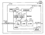
- FIG. 14 is a block diagram illustrating a configuration of the OLT device 100a according to the embodiment.
- the OLT device 100a includes an optical transceiver unit 101A and a MAC unit 102.
- the optical transceiver unit 101A includes a power saving control unit 101a, a receiving unit 101b, a power saving mode flag generating unit 101e, a packet monitoring unit 101f, and a pattern identifying unit 101g.
- the power saving control unit 101a performs power saving control of the receiving unit 101b of the OLT device 100a based on the power saving mode flag generated by the power saving mode flag generating unit 101e.
- the power saving mode flag generation unit 101e generates a power saving mode flag based on the packet transmission timing information obtained by the packet monitoring unit 101f and the reset signal output from the MAC unit 102.
- the packet monitoring unit 101f monitors packets transmitted from each ONT device 200ai.
- the pattern identification unit 101g identifies the packet in the data communication area and the packet in the ranging area, and outputs the identification result to the power saving mode flag generation unit 101e.
- the packet monitoring unit 101f monitors a packet transmitted from the ONT device 200ai, and includes a signal disconnection detection unit 101f1 as shown in FIG.
- the power saving mode flag generation unit 101e activates the power saving mode flag (non-power saving mode, power-on).
- the power saving mode flag generation unit 101e sets the power saving mode flag to sleep (power saving mode, power off) by the signal interruption detection signal obtained by the signal interruption detection unit 101f1 of the packet monitoring unit 101f.
- the power saving mode flag generation unit 101e activates the power saving mode flag and changes the sleep depending on the packet state in the packet data communication area, but always activates in the ranging area.
- the identification of the data communication area or the ranging area of the packet is performed by the pattern identification unit 101g.
- the pattern stored in a predetermined storage area not shown for reference is compared with the pattern of the packet in advance. Identify more.
- the power saving control unit 101a turns on / off the power of the receiving unit 101b based on the power saving mode flag.
- power saving is achieved by turning on / off the power of the receiving unit 101b of the optical transceiver unit 101A (not all circuit blocks but also some circuit blocks) according to the state of the packet. Is possible. Furthermore, during ranging, it is possible to perform ranging normally by always turning on the power of the receiving unit 101b regardless of the packet state.
- FIG. 15 is a diagram illustrating a detailed configuration of the power saving mode flag generation unit 101e.
- the power saving mode flag generation unit 101e includes a latch unit 101e1, an OR unit 101e2, a timer unit 101e3, a mask signal generation unit 101e4, and a delay unit 101e5.
- the latch unit 101e1 receives a reset signal from the MAC 102.
- the reset signal is one of control signals generally used in the OLT device 101a, and is a signal generated immediately before each packet based on ranging information for the purpose of threshold initialization of the optical transceiver unit 101A.
- the latch unit 101e1 has a function of detecting and latching (holding) a reset signal and resetting by a signal disconnection detection signal input from the delay unit 101e5.
- the latch unit 101e1 outputs a reset signal H (ON) or L (OFF) to the OR unit 101e2.
- the delay unit 101e5 delays the signal interruption detection signal obtained from the packet monitoring unit 101f until a predetermined condition is satisfied.
- the predetermined condition will be described later.
- the timer unit 101e3 receives a detection signal obtained by detecting the first packet signal in the data communication area within the delay measurement window identified by the pattern identification unit 101g, and receives a preset ranging area. Time.
- the timer unit 101e3 outputs a time measurement end signal to the mask signal generation unit 101e4 when the time measurement until receiving the preset ranging area is completed.
- the mask signal generation unit 101e4 generates a mask signal that is H (on) during ranging and L (off) otherwise, based on the timing end signal input from the timer unit 101e3. Then, the mask signal generation unit 101e4 outputs a mask signal to the OR unit 101e2.
- the OR unit 101e2 is a logic gate that calculates the logical sum of the reset signal input from the latch unit 101e1 and the mask signal input from the mask signal generation unit 101e4.
- the OR unit 101e2 outputs a logical sum of the reset signal and the mask signal to the power saving control unit 101a1 as a power saving mode flag.
- the signal output from the OR unit 101e2 is a power saving mode flag. In the data communication area, the power saving mode flag is changed to the active mode or the sleep mode depending on the packet state, but in the ranging area, the signal is always set to the active mode. Become.
- FIG. 16A is a diagram illustrating a circuit example of the delay unit 101e5.
- the delay unit 101e5 includes an inverting gate 101e5a, a resistor 101e5b, a diode 101e5c, a capacitor 101e5d, and an inverting gate 101e5e.
- the inverting gate 101e5a inverts the signal interruption detection signal input from the packet monitoring unit 101f and outputs the inverted signal to the resistor 101e5b.
- a grounded capacitor is connected to the signal output destination of the resistor 101e5b.
- a diode (commutator) 101e5c that inputs the signal output of the resistor 101e5b by looping back to the resistor 101e5b is connected.
- an inversion gate 101e5e that further inverts the signal output of the resistor 101e5b and outputs it to the latch unit 101e1 is connected.
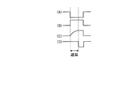
- [Time chart of delay part] 16B is a time chart illustrating signal states at (A) to (D) of the circuit of the delay unit 101e5 illustrated in FIG.
- the amount of delay can be varied by adjusting the capacitor value of the capacitor 101e5d. Further, only the falling edge of the output signal is delayed, and the rising edge is not delayed.
- the delay time is preferably about guard time (25-30 ns for GPON).
- the signal in (A) is a signal loss detection signal.
- the signal in (B) is a signal obtained by inverting the signal break detection signal.
- the signal at the point (C) is a signal in which the voltage drop due to the resistor 101e5b is gradually canceled by the charging of the capacitor 101e5d and the edge gradually rises.
- the signal at the point (D) outputs an inverted signal of the signal at the point (C) only when the signal at the point (C) becomes H (ON). Therefore, the time until the signal at point (C) becomes H (ON) after the signal interruption detection signal is input is the delay time delayed by the delay unit 101e5.
- the above-described predetermined condition that defines the time for delaying the signal interruption detection signal obtained from the packet monitoring unit 101f is that the charging of the capacitor 101e5d is completed.
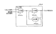
- FIG. 17 is a diagram illustrating a circuit example of the latch circuit unit 101e1.
- the latch circuit unit 101e1 detects and latches the input of the reset signal from the MAC unit 102, and resets the reset signal latch by the input of the output signal from the delay unit 105e.
- the latch circuit unit 101e1 includes an OR unit 101e1a, an OR unit 101e1b, and an AND unit 101e1c.
- the OR unit 101e1a outputs a logical sum having the input of the reset signal from the MAC unit 102 and the output signal from the delay unit 105e to the OR unit 101e1b and the AND unit 101e1c.
- the OR unit 101e1b outputs a logical sum having the outputs of the OR unit 101e1a and the AND unit 101e1c as inputs to the OR unit 101e2 of the power saving mode flag generation unit 101e and also outputs to the AND unit 101e1c.
- the AND unit 101e1c outputs a logical product having the outputs of the OR unit 101e1a and the OR unit 101e1b as inputs to the OR unit 101e1b.
- FIG. 18 is a diagram illustrating the optical transceiver unit 101A including the packet monitoring unit 101f.
- the packet monitoring unit 101f includes a signal disconnection detection unit 101f1.
- the signal disconnection detection unit 101f1 receives an input of a packet signal indicated by a voltage output from the PD / TIA unit 101b1 of the reception unit 101b. The presence or absence of packet signal input is detected and notified to the power saving mode flag generation unit 101e.
- FIG. 19 is a diagram illustrating a circuit example of the signal disconnection detection unit 101f1.
- the signal interruption detection unit 101f1 includes an AMP unit 101f1a that is a preamplifier that amplifies an input signal, a peak detection unit 101f1b that detects a peak of an output of the AMP unit 101f1a, and a bottom detection unit 101f1c that detects a bottom of an output of the AMP unit 101f1a.
- a threshold storage unit 101f1d that stores a voltage threshold for identifying H (ON) and L (OFF) of the signal, an output of the peak detection unit 101f1b and an output of the bottom detection unit 101f1c, and an output of the threshold storage unit 101f1d
- a CMP unit 101f1f that is a comparator that compares the output of the threshold value is included. Also included is an adding unit 101f1e that adds the output of the threshold value of the threshold storage unit 101f1d to the output of the bottom detection unit 101f1c.
- the CMP unit 101f1f outputs a signal with a packet when the output of the bottom detection unit 101f1c exceeds the threshold value. Further, the CMP unit 101f1f outputs a signal indicating no packet (signal disconnection detection signal) when the output of the peak detection unit 101f1v is below the threshold value.
- the output signal of the signal loss detection unit 101f1 may be an analog signal or a digital signal. Further, the output signal of the signal break detection unit 101f1 may be a serial signal or a parallel signal.
- the optical transceiver unit 101A includes a PD / TIA unit 101b1, a limiter amplifier LIM unit 101b2, and an output unit 101b3.
- FIG. 20 is a diagram illustrating a circuit example of the PD / TIA unit 101b1.
- the PD / TIA unit 101b1 is a photoelectric unit that receives an optical signal and converts it into an electrical signal.
- the TIA unit 101b amplifies the electrical signal converted by the PD unit 101b1a and converts the electrical signal into a voltage signal. including.
- FIG. 21 is a diagram illustrating a circuit example of the LIM unit 101b2.
- the LIM unit 101b2 includes a peak detection unit 101b2b that detects a peak of the electrical signal that is finally converted into a voltage signal by the PD / TIA unit 101b1, a bottom detection unit 101b2c that detects the bottom of the electrical signal, and a peak of the peak detection unit 101b2b.
- a resistor 101b2d for dropping the voltage of the output and a resistor 101b2e for dropping the voltage of the bottom output of the bottom detection unit 101b2c are included.
- the AMP unit is an amplifier that receives the voltage signal input by the PD / TIA unit 101b1, and the peak voltage signal and the bottom voltage signal that have been dropped by the resistor 101b2d and the resistor 101b2e, and amplifies and outputs both of them. 101b2a is included.
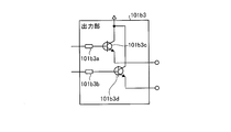
- FIG. 22 is a diagram illustrating a circuit example of the output unit 101b3.
- the output unit 101b3 includes a resistor 101b3a, a resistor 101b3b, a transistor 101b3c, and a transistor 101b3d.
- the transistor 101b3c uses a direct voltage signal output from the PD / TIA unit 101b1 and directly amplified by the LIM unit 101b2 as a base signal.
- the transistor 101b3d uses the peak voltage signal and the bottom voltage signal amplified by the LIM unit 101b2 as base signals.
- the collector terminals of the transistors 101b3c and 101b3d are connected to each other. As a result, if there is even a slight current difference between the direct voltage signal and the peak voltage signal and the bottom voltage signal, the direct voltage signal, the peak voltage signal, and the bottom voltage signal output a large current from each collector terminal. be able to.
- FIG. 23 is a diagram illustrating a detailed configuration of the power saving control unit 101a1.
- the power saving control unit 101a1 controls the power on / off of the receiving unit 101b based on the control signal (power saving mode flag) generated and output by the power saving mode flag generating unit 101e.
- the power saving control unit 101a1 includes a power supply unit 101a1a and a switch function unit 101a1b.
- the power supply unit 101a1a is a power supply that supplies power to the receiving unit 101b.
- the switch function unit 101a1b turns on / off the power supplied from the power supply unit 101a1a. Note that the power on / off target may be a specific functional block instead of the functional blocks of all receiving units.
- FIG. 24 is a block diagram illustrating a configuration of an OLT device 100a2 according to an application example of the disclosed technology.
- a light intensity detection unit 101h is provided as an alternative to the reset signal from the MAC unit 102 according to the embodiment.
- FIG. 25 is a block diagram illustrating a detailed configuration of a light intensity detection unit according to an application example of the disclosed technology.
- the light intensity detection unit 101h includes a current monitoring unit 101h1, a comparison unit 101h2, a pulse generation unit 101h3, and a threshold storage unit 101h4.
- the current monitor unit 101h1 detects an APD (Avalanche Photo Diode) current value.
- the APD current increases in current value according to the light intensity.
- the comparison unit 101h2 compares the APD current value with a preset threshold value stored in the threshold value storage unit 101h4. As a result of comparison, when the APD current value exceeds the threshold value, it is asserted (validated), and the pulse generated by the pulse generation unit 101h3 is output. The pulse becomes an input signal of the latch unit 101e1 in the power saving mode flag generation unit 101e.
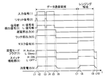
- FIG. 26 is a time chart illustrating the power saving control process according to the embodiment and the application example.
- the horizontal axis represents the time axis of one delay measurement frame.
- the delay measurement frame is divided into a data communication area and a ranging area.
- FIG. 26 (1) shows a packet signal transmitted from the ONT device 200ai to the OLT device 100.
- FIG. (2) indicates a reset signal (or APD current value). The reset signal is input immediately before each packet.
- (3) shows the output of the signal break detection unit 101f1. (3) is asserted (validated) when a preset threshold value for determining the presence or absence of a packet is exceeded based on the input signal of (1). Deassert (invalidate) when there is no packet signal.
- (6) indicates an output signal from the mask signal generation unit 101e4. Only the ranging area in the delay measurement frame is “H”, and the others are “L”. (7) shows the output signal of the power saving mode flag. This is the logical sum of the signals (5) and (6). (8) is a time chart of the output of the switch function unit 101a1b in the power saving control unit 101a1. The timing is the same as that of the power saving mode flag (7) and the signal.
- (9) indicates the power consumption of the OLT device 100a and the OLT device 100a2.
- the switch function unit 101a1b of (8) is switched off, the power of the block of the reception unit 101b is turned off, so that power consumption is reduced. That is, power consumption can be suppressed in the data communication area according to the presence or absence of a packet.
- the power saving mode flag is always “H”, the switch of the switch function unit 101a1b is always on.
- the power saving method that can follow the increase / decrease of the real-time packet accompanying the increase / decrease of the ONT device 200ai of the PON system and that can be applied at the time of ranging specific to the PON system is applied. It becomes possible. In addition, by reducing power consumption, it is possible to reduce the amount of heat generation and improve the integration degree of the OLT devices, that is, increase the number of ONT devices 200ai accommodated by the OLT device 100a and the OLT device 100a2. It becomes. That is, it becomes possible to control the power supplies of the circuit blocks of the OLT device 100a and the OLT device 100a2 in real time according to the state of the optical communication network.
- the present invention can be widely applied to an OLT device that is a main terminal device of a network.
- each component of each illustrated apparatus is functionally conceptual and does not necessarily need to be physically configured as illustrated.
- the specific form of distribution / integration of each device is not limited to that shown in the figure, and all or a part thereof may be functionally or physically distributed or arbitrarily distributed in arbitrary units according to various loads or usage conditions. Can be integrated and configured.
- Optical transceiver unit 101a 101a1 Power saving control unit 101a1a Power supply unit 101a1b Switch function unit 101b Receiver unit 101b1 PD / TIA unit 101b1a PD unit 101b2 LIM unit 101b2a AMP unit 101b2b Peak detection unit 101b2c Bottom detection unit 101b2d, 101b2e Resistance 101b3 Output unit 101b3a, 101b3b Resistance 101b3c, 101b3d Transistor 101c Packet information storage unit 101d Timer unit 101e Power saving mode flag generation unit 101e1 Latch unit 101e1 101e1b OR unit 101e1c AND unit 101e2 OR unit 101e3 Timer unit 101e4 Mask signal generation unit 101 e5 delay unit 101e5a, 101e5e inverting gate 101e5b resistor 101e5c diode 101e5d capacitor 101f packet monitoring unit 101f1 signal
Landscapes
- Engineering & Computer Science (AREA)
- Computer Networks & Wireless Communication (AREA)
- Signal Processing (AREA)
- Small-Scale Networks (AREA)
- Optical Communication System (AREA)
Abstract
L'invention concerne une unité de surveillance de paquets (101f) qui surveille des paquets émis par un dispositif ONT (200ai) et qui comprend une unité de détection d'arrêt de signal (101f1). Une unité de production de drapeau de mode d'économie d'énergie (101e) active un drapeau de mode d'économie d'énergie (mode sans économie d'énergie, entrée d'alimentation électrique) lorsqu'un signal de réinitialisation est fourni par une unité MAC (102). L'unité de production de drapeau de mode d'économie d'énergie (101e) place également le drapeau de mode d'économie d'énergie dans l'état au repos (mode d'économie d'énergie, coupure d'alimentation électrique) à l'aide d'un signal de détection d'arrêt de signal obtenu par l'unité de détection d'arrêt de signal (101f1) dans l'unité de surveillance de paquet (101f). L'unité de production de drapeau de mode d'économie d'énergie (101e) place le drapeau de mode d'économie d'énergie dans l'état actif ou dans l'état au repos en fonction de l'état du paquet dans une région de communication de données en paquets, mais place toujours le drapeau de mode d'économie d'énergie dans son état actif dans une région de mesure. Une unité de discrimination de motifs (101g) fait la différence entre la région de communication de données en paquets et la région de mesure.
Priority Applications (3)
| Application Number | Priority Date | Filing Date | Title |
|---|---|---|---|
| PCT/JP2009/060962 WO2010146665A1 (fr) | 2009-06-16 | 2009-06-16 | Dispositif de communication optique et procédé de commande économe en énergie pour un dispositif de communication optique |
| JP2011519344A JP5263394B2 (ja) | 2009-06-16 | 2009-06-16 | 光通信装置及び光通信装置の節電制御方法 |
| US13/328,666 US8559814B2 (en) | 2009-06-16 | 2011-12-16 | Optical communication device and power-saving control method of optical communication device |
Applications Claiming Priority (1)
| Application Number | Priority Date | Filing Date | Title |
|---|---|---|---|
| PCT/JP2009/060962 WO2010146665A1 (fr) | 2009-06-16 | 2009-06-16 | Dispositif de communication optique et procédé de commande économe en énergie pour un dispositif de communication optique |
Related Child Applications (1)
| Application Number | Title | Priority Date | Filing Date |
|---|---|---|---|
| US13/328,666 Continuation US8559814B2 (en) | 2009-06-16 | 2011-12-16 | Optical communication device and power-saving control method of optical communication device |
Publications (1)
| Publication Number | Publication Date |
|---|---|
| WO2010146665A1 true WO2010146665A1 (fr) | 2010-12-23 |
Family
ID=43356003
Family Applications (1)
| Application Number | Title | Priority Date | Filing Date |
|---|---|---|---|
| PCT/JP2009/060962 Ceased WO2010146665A1 (fr) | 2009-06-16 | 2009-06-16 | Dispositif de communication optique et procédé de commande économe en énergie pour un dispositif de communication optique |
Country Status (3)
| Country | Link |
|---|---|
| US (1) | US8559814B2 (fr) |
| JP (1) | JP5263394B2 (fr) |
| WO (1) | WO2010146665A1 (fr) |
Cited By (5)
| Publication number | Priority date | Publication date | Assignee | Title |
|---|---|---|---|---|
| JP2012039249A (ja) * | 2010-08-04 | 2012-02-23 | Mitsubishi Electric Corp | 光アクセスシステムの局側装置 |
| CN102546000A (zh) * | 2012-01-18 | 2012-07-04 | 索尔思光电(成都)有限公司 | 一种epon olt节能控制方法及系统 |
| JP2012138792A (ja) * | 2010-12-27 | 2012-07-19 | Nec Corp | 局側光終端装置と加入者側光終端装置及びその制御方法と制御プログラム |
| JP2013034143A (ja) * | 2011-08-03 | 2013-02-14 | Nippon Telegr & Teleph Corp <Ntt> | 光回線終端装置および鍵切替方法 |
| WO2013183628A1 (fr) * | 2012-06-04 | 2013-12-12 | 日本電信電話株式会社 | Terminal de ligne optique et procédé de transfert de trame |
Families Citing this family (11)
| Publication number | Priority date | Publication date | Assignee | Title |
|---|---|---|---|---|
| US8787751B2 (en) * | 2009-04-22 | 2014-07-22 | Futurewei Technologies, Inc. | Method for identifying the optical network unit power off reason |
| KR101287334B1 (ko) * | 2009-07-14 | 2013-07-23 | 미쓰비시덴키 가부시키가이샤 | 광 종단국 장치 및 pon 시스템 |
| US20120045202A1 (en) * | 2010-08-17 | 2012-02-23 | Xu Jiang | High Speed Bi-Directional Transceiver, Circuits and Devices Therefor, and Method(s) of Using the Same |
| KR101327554B1 (ko) * | 2010-12-23 | 2013-11-20 | 한국전자통신연구원 | 광망종단 장치 및 그것의 전력 절감 방법 |
| WO2012176894A1 (fr) * | 2011-06-24 | 2012-12-27 | 日本電信電話株式会社 | Système de communication, procédé de communication et station enfant d'un système de communication |
| CN103236882B (zh) * | 2013-04-26 | 2016-10-26 | 上海交通大学 | 一种twdm-pon系统中olt的节能方法 |
| US9766689B2 (en) * | 2013-12-24 | 2017-09-19 | Lenovo Enterprise Solutions (Singapore) Pte. Ltd. | Effective power management for pluggable transceiver receiving hardware in network switching systems |
| US9294290B2 (en) * | 2014-07-15 | 2016-03-22 | Corning Optical Communications LLC | Optical cable assemblies with low-speed data pass-through architecture and sleep mode operation |
| US9755746B1 (en) * | 2014-10-03 | 2017-09-05 | Adtran, Inc. | Systems and methods for digitally splitting an optical line terminal across multiple fibers |
| US10009673B1 (en) * | 2017-09-15 | 2018-06-26 | Futurewei Technologies, Inc. | Efficient CPRI transmission |
| US11032010B1 (en) * | 2020-03-11 | 2021-06-08 | Charter Communications Operating, Llc | Methods and apparatus for reducing power consumption in optical devices |
Citations (3)
| Publication number | Priority date | Publication date | Assignee | Title |
|---|---|---|---|---|
| JP2004104278A (ja) * | 2002-09-06 | 2004-04-02 | Fujitsu Ltd | Pon伝送システム |
| JP2007043270A (ja) * | 2005-08-01 | 2007-02-15 | Hitachi Communication Technologies Ltd | Wdm型ponシステム |
| WO2008038981A1 (fr) * | 2006-09-29 | 2008-04-03 | Electronics And Telecommunications Research Institute | Procédé de commande de puissance optique automatique pour terminal olt dans un réseau pon |
Family Cites Families (27)
| Publication number | Priority date | Publication date | Assignee | Title |
|---|---|---|---|---|
| US5504606A (en) * | 1994-06-01 | 1996-04-02 | At&T Corp. | Low power optical network unit |
| JP3425012B2 (ja) | 1995-08-29 | 2003-07-07 | 松下電器産業株式会社 | 2線式給電通信装置 |
| KR19990079584A (ko) * | 1998-04-07 | 1999-11-05 | 윤종용 | 사용자 감지 장치를 갖는 저소비 전력용 컴퓨터 시스템 및 그의전원 공급 제어 방법 |
| JP3520408B2 (ja) | 1998-11-30 | 2004-04-19 | 日本電信電話株式会社 | マルチレート伝送システムにおけるフレーム同期方法及びこれに用いる送信装置,送受信装置 |
| JP4328459B2 (ja) * | 2000-10-27 | 2009-09-09 | Necエンジニアリング株式会社 | ネットワークのサービス品質測定システム及びその方法 |
| CN100512187C (zh) * | 2001-06-29 | 2009-07-08 | 三菱电机株式会社 | 分组通信系统以及分组通信方法 |
| JP3872716B2 (ja) * | 2002-04-30 | 2007-01-24 | 富士通株式会社 | パケット出力制御装置 |
| KR100665457B1 (ko) * | 2003-04-30 | 2007-01-04 | 삼성전자주식회사 | 광대역 무선 접속 통신 시스템에서 슬립 모드 및 어웨이크 모드에서의 상태 천이 제어 시스템 및 방법 |
| FR2857530B1 (fr) * | 2003-07-11 | 2005-09-23 | Cit Alcatel | Reseau optique en anneau a protocole de remplissage de trous independant du debit |
| JP2006211480A (ja) * | 2005-01-31 | 2006-08-10 | Sanyo Electric Co Ltd | データ送信装置及びデータ収集システム |
| US7734173B2 (en) * | 2005-02-25 | 2010-06-08 | Dynamic Method Enterprises Limited | Error detection and recovery of an optical network element |
| US7441061B2 (en) * | 2005-02-25 | 2008-10-21 | Dynamic Method Enterprises Limited | Method and apparatus for inter-module communications of an optical network element |
| US7536489B2 (en) * | 2005-08-30 | 2009-05-19 | Ricoh Company Limited | Information processing system for determining payload size based on packet-to-payload size ratio |
| US8171312B2 (en) * | 2006-07-05 | 2012-05-01 | Canon Kabushiki Kaisha | Recording apparatus and method for controlling the recording apparatus |
| JP4737035B2 (ja) * | 2006-10-30 | 2011-07-27 | 日本電気株式会社 | QoSルーティング方法およびQoSルーティング装置 |
| JP5028179B2 (ja) * | 2007-08-03 | 2012-09-19 | 株式会社日立製作所 | Ponシステム |
| US8588118B2 (en) * | 2007-08-24 | 2013-11-19 | Kabushiki Kaisha Toshiba | Wireless communication device and wireless communication system |
| JP4772150B2 (ja) * | 2007-12-07 | 2011-09-14 | アライドテレシスホールディングス株式会社 | 通信装置 |
| US8000602B2 (en) * | 2008-04-17 | 2011-08-16 | Pmc-Sierra Israel Ltd. | Methods and devices for reducing power consumption in a passive optical network while maintaining service continuity |
| US8275261B2 (en) * | 2008-04-17 | 2012-09-25 | Pmc Sierra Ltd | Power saving in IEEE 802-style networks |
| US8521033B2 (en) * | 2009-06-10 | 2013-08-27 | Alcatel Lucent | System and method for energy-efficient operation of optical network units based on scheduled payload reception |
| WO2011092822A1 (fr) * | 2010-01-28 | 2011-08-04 | 三菱電機株式会社 | Procédé de commande de bande, système de communication et dispositif de communication |
| JP2011170709A (ja) * | 2010-02-19 | 2011-09-01 | Ricoh Co Ltd | ネットワーク制御装置、画像形成装置、画像形成システム、省エネ制御方法、及び省エネ制御プログラム |
| JP5463165B2 (ja) * | 2010-02-26 | 2014-04-09 | 株式会社日立製作所 | 省電力化可能なponシステムにおける、onuのスリープ状態からの復旧方法 |
| JP4812884B2 (ja) * | 2010-04-13 | 2011-11-09 | 三菱電機株式会社 | 通信システム、局側光回線終端装置、利用者側光回線終端装置、制御装置、並びに通信方法 |
| KR101746629B1 (ko) * | 2010-05-31 | 2017-06-13 | 가부시키가이샤 진-매직 | 통신 장치 및 통신 방법 |
| US8565601B2 (en) * | 2010-12-08 | 2013-10-22 | Mitsubishi Electric Corporation | Communication method for optical communication system, optical communication system, slave station apparatus, control device, and computer program |
-
2009
- 2009-06-16 WO PCT/JP2009/060962 patent/WO2010146665A1/fr not_active Ceased
- 2009-06-16 JP JP2011519344A patent/JP5263394B2/ja not_active Expired - Fee Related
-
2011
- 2011-12-16 US US13/328,666 patent/US8559814B2/en not_active Expired - Fee Related
Patent Citations (3)
| Publication number | Priority date | Publication date | Assignee | Title |
|---|---|---|---|---|
| JP2004104278A (ja) * | 2002-09-06 | 2004-04-02 | Fujitsu Ltd | Pon伝送システム |
| JP2007043270A (ja) * | 2005-08-01 | 2007-02-15 | Hitachi Communication Technologies Ltd | Wdm型ponシステム |
| WO2008038981A1 (fr) * | 2006-09-29 | 2008-04-03 | Electronics And Telecommunications Research Institute | Procédé de commande de puissance optique automatique pour terminal olt dans un réseau pon |
Cited By (6)
| Publication number | Priority date | Publication date | Assignee | Title |
|---|---|---|---|---|
| JP2012039249A (ja) * | 2010-08-04 | 2012-02-23 | Mitsubishi Electric Corp | 光アクセスシステムの局側装置 |
| JP2012138792A (ja) * | 2010-12-27 | 2012-07-19 | Nec Corp | 局側光終端装置と加入者側光終端装置及びその制御方法と制御プログラム |
| JP2013034143A (ja) * | 2011-08-03 | 2013-02-14 | Nippon Telegr & Teleph Corp <Ntt> | 光回線終端装置および鍵切替方法 |
| CN102546000A (zh) * | 2012-01-18 | 2012-07-04 | 索尔思光电(成都)有限公司 | 一种epon olt节能控制方法及系统 |
| CN102546000B (zh) * | 2012-01-18 | 2015-04-15 | 索尔思光电(成都)有限公司 | 一种epon olt节能控制方法及系统 |
| WO2013183628A1 (fr) * | 2012-06-04 | 2013-12-12 | 日本電信電話株式会社 | Terminal de ligne optique et procédé de transfert de trame |
Also Published As
| Publication number | Publication date |
|---|---|
| US8559814B2 (en) | 2013-10-15 |
| JPWO2010146665A1 (ja) | 2012-11-29 |
| US20120087652A1 (en) | 2012-04-12 |
| JP5263394B2 (ja) | 2013-08-14 |
Similar Documents
| Publication | Publication Date | Title |
|---|---|---|
| JP5263394B2 (ja) | 光通信装置及び光通信装置の節電制御方法 | |
| US9106984B2 (en) | PON system, subscriber-side terminal apparatus, station-side terminal apparatus, and power saving method | |
| US8744261B2 (en) | EPON with power-saving features | |
| US11804909B2 (en) | Power saving mechanisms for high speed passive optical network | |
| JP2021511759A (ja) | Olt、onu、ponシステム、及びponシステムにおけるメッセージ伝送方法 | |
| CN108476082B (zh) | 多信道无源光网络中信道控制方法及光线路终端和光网络单元 | |
| US8879594B2 (en) | Efficient power control for an automatic laser driver | |
| US9712254B2 (en) | Current-voltage conversion circuit, optical receiver, and optical terminator | |
| JP2010226693A (ja) | Ponシステムの局側終端装置 | |
| JP5067610B2 (ja) | Ponシステムにおける局側端局装置 | |
| KR20150042630A (ko) | 슬립모드 onu 제어 기법 | |
| KR100762605B1 (ko) | 이더넷 수동형 광 가입자망의 광 가입자 장치 및 제어 방법 | |
| JP2010004356A (ja) | 光通信システムに設置される監視装置及び監視回路 | |
| US20110076012A1 (en) | Optical network terminal and method for detecting transmission error in optical network terminal | |
| JP2012156954A (ja) | 局側装置、宅側装置および通信システム | |
| JP5084629B2 (ja) | 加入者終端装置および電源制御方法 | |
| JP5761415B1 (ja) | 加入者側装置登録方法 | |
| US8463139B2 (en) | Transmitter disabling device | |
| KR101063012B1 (ko) | 시분할 다중접속 방식의 수동 광가입자망을 구성하는 광 회선 단말 및 광 회선 단말의 연속모드 수신기 | |
| KR101385390B1 (ko) | Epon 시스템에서 단말 장치의 슬립 모드 동작 방법 및 이를 구현하는 단말 장치 | |
| JP2014086989A (ja) | 子局装置、1対n通信システム及び子局装置の消費電力制御プログラム | |
| Wu et al. | An ultra-long haul PON trunk fiber protector based on SOA | |
| JP2014072619A (ja) | 通信装置および通信システム |
Legal Events
| Date | Code | Title | Description |
|---|---|---|---|
| 121 | Ep: the epo has been informed by wipo that ep was designated in this application |
Ref document number: 09846158 Country of ref document: EP Kind code of ref document: A1 |
|
| WWE | Wipo information: entry into national phase |
Ref document number: 2011519344 Country of ref document: JP |
|
| NENP | Non-entry into the national phase |
Ref country code: DE |
|
| 122 | Ep: pct application non-entry in european phase |
Ref document number: 09846158 Country of ref document: EP Kind code of ref document: A1 |