WO2010146706A1 - Dispositif laser à guide d'ondes plan et écran utilisant le dispositif laser - Google Patents
Dispositif laser à guide d'ondes plan et écran utilisant le dispositif laser Download PDFInfo
- Publication number
- WO2010146706A1 WO2010146706A1 PCT/JP2009/061208 JP2009061208W WO2010146706A1 WO 2010146706 A1 WO2010146706 A1 WO 2010146706A1 JP 2009061208 W JP2009061208 W JP 2009061208W WO 2010146706 A1 WO2010146706 A1 WO 2010146706A1
- Authority
- WO
- WIPO (PCT)
- Prior art keywords
- laser
- light
- laser medium
- medium
- refractive index
- Prior art date
- Legal status (The legal status is an assumption and is not a legal conclusion. Google has not performed a legal analysis and makes no representation as to the accuracy of the status listed.)
- Ceased
Links
Images




Classifications
-
- H—ELECTRICITY
- H01—ELECTRIC ELEMENTS
- H01S—DEVICES USING THE PROCESS OF LIGHT AMPLIFICATION BY STIMULATED EMISSION OF RADIATION [LASER] TO AMPLIFY OR GENERATE LIGHT; DEVICES USING STIMULATED EMISSION OF ELECTROMAGNETIC RADIATION IN WAVE RANGES OTHER THAN OPTICAL
- H01S3/00—Lasers, i.e. devices using stimulated emission of electromagnetic radiation in the infrared, visible or ultraviolet wave range
- H01S3/05—Construction or shape of optical resonators; Accommodation of active medium therein; Shape of active medium
- H01S3/06—Construction or shape of active medium
- H01S3/063—Waveguide lasers, i.e. whereby the dimensions of the waveguide are of the order of the light wavelength
- H01S3/0632—Thin film lasers in which light propagates in the plane of the thin film
-
- G—PHYSICS
- G02—OPTICS
- G02F—OPTICAL DEVICES OR ARRANGEMENTS FOR THE CONTROL OF LIGHT BY MODIFICATION OF THE OPTICAL PROPERTIES OF THE MEDIA OF THE ELEMENTS INVOLVED THEREIN; NON-LINEAR OPTICS; FREQUENCY-CHANGING OF LIGHT; OPTICAL LOGIC ELEMENTS; OPTICAL ANALOGUE/DIGITAL CONVERTERS
- G02F1/00—Devices or arrangements for the control of the intensity, colour, phase, polarisation or direction of light arriving from an independent light source, e.g. switching, gating or modulating; Non-linear optics
- G02F1/35—Non-linear optics
- G02F1/355—Non-linear optics characterised by the materials used
- G02F1/3551—Crystals
-
- H—ELECTRICITY
- H01—ELECTRIC ELEMENTS
- H01S—DEVICES USING THE PROCESS OF LIGHT AMPLIFICATION BY STIMULATED EMISSION OF RADIATION [LASER] TO AMPLIFY OR GENERATE LIGHT; DEVICES USING STIMULATED EMISSION OF ELECTROMAGNETIC RADIATION IN WAVE RANGES OTHER THAN OPTICAL
- H01S3/00—Lasers, i.e. devices using stimulated emission of electromagnetic radiation in the infrared, visible or ultraviolet wave range
- H01S3/09—Processes or apparatus for excitation, e.g. pumping
- H01S3/091—Processes or apparatus for excitation, e.g. pumping using optical pumping
- H01S3/094—Processes or apparatus for excitation, e.g. pumping using optical pumping by coherent light
- H01S3/0941—Processes or apparatus for excitation, e.g. pumping using optical pumping by coherent light of a laser diode
- H01S3/09415—Processes or apparatus for excitation, e.g. pumping using optical pumping by coherent light of a laser diode the pumping beam being parallel to the lasing mode of the pumped medium, e.g. end-pumping
Definitions
- the present invention relates to a planar waveguide laser device for realizing a high-power laser device and a wavelength conversion laser device suitable for use in a light source for a printer, a laser TV, or a laser processing machine.
- printers and displays require light sources of three colors R (red), G (green), and B (blue) as light sources, and wavelength conversion lasers have been developed as such light sources. .
- the wavelength conversion laser uses second-order harmonics (SHG: Second Harmonic Generation) and third-order harmonics (THG) using nonlinear materials, using 900 nm band, 1 ⁇ m band, and 1.3 ⁇ m band laser beams as fundamental laser beams. : Wavelength conversion to higher harmonics such as Third Harmonic Generation).
- the two-dimensional waveguide laser can increase the power density of the fundamental laser beam, it is possible to achieve a high conversion efficiency to the harmonic laser beam. There is a limit to high output. Also, since there is a limit to LD (laser diode) light having a good beam quality in a two-dimensional direction that can be coupled to a two-dimensional waveguide, there is a limit to increasing the output.
- LD laser diode
- a planar waveguide laser device having a one-dimensional waveguide for example, see Non-Patent Document 1.
- laser oscillation is performed in a spatial mode in a direction perpendicular to the laser optical axis within a flat plate surface, and the beam diameter of the laser beam is expanded in this direction, or the laser beam is multiplexed.
- High output is planned.
- the LD output light that is the excitation source only needs to be coupled to the planar waveguide in a one-dimensional direction, so that a high output broad area LD can be used as a light source. High output laser light can be obtained.
- the multi-emitter LDs arranged in a one-dimensional direction can be used as the emission point of the LD output light, it is possible to obtain a larger laser output.
- the fundamental laser beam can be generated by using a planar waveguide type laser medium and generating a gain to perform laser resonance.
- the harmonics are obtained by wavelength-converting the fundamental laser beam using a planar waveguide type wavelength conversion element (nonlinear material).
- the laser medium excited by the LD output light emits spontaneously emitted light in all directions, but resonates in the laser optical axis direction to perform laser oscillation.
- the gain in the laser optical axis direction decreases and the laser output power decreases. become.
- spontaneous emission light having an angle including a component orthogonal to the laser optical axis in the flat plate surface of the planar waveguide may propagate through the waveguide at that angle and be amplified.
- a broad area type semiconductor laser having a wide width in the direction perpendicular to the laser optical axis in the flat plate surface is used as an excitation source, or a multi-emitter type semiconductor laser in which a plurality of light emitting points are arranged
- the gain received by spontaneously emitted light propagating at an angle that includes a component perpendicular to the laser optical axis within the flat plate surface increases, so that unintended parasitic oscillation and parasitic amplification occur. May occur.
- unintentional extraction of energy decreases the gain in the laser optical axis direction and a high-power laser output cannot be obtained.
- planar waveguide type laser medium has a thin flat plate shape
- a substrate may be attached to the upper part of the laser medium for the purpose of ensuring mechanical strength.
- a low refractive index cladding layer is disposed on the upper and lower surfaces of a flat plate surface in order to propagate light as a waveguide.
- bonding may be performed using a bonding agent such as an adhesive, or bonding may be performed using diffusion bonding, optical contact, or the like.
- a brazing material to which an active medium in the laser medium is not added may be used in order to match the linear expansion coefficient and mechanical characteristics with the laser medium.
- Nd neodymium
- YVO4 yttrium vanadate
- the refractive index change due to the addition of an active medium such as Nd is minute, the refractive indexes of the laser medium and the substrate are almost equal.
- the laser medium can be propagated as a waveguide.
- the propagating light direction is substantially parallel to the waveguide laser optical axis (shallow angle component), and the component having a large angle with respect to the waveguide thickness direction passes through the cladding. Leak to the board side.
- spontaneous emission light is radiated in all directions, so there is light that leaks to the substrate side through the cladding, and further, a part of the light is transmitted through the upper surface of the substrate in contact with air, Some are totally reflected.
- the substrate above the cladding has a high refractive index equivalent to that of the laser medium
- Fresnel reflection occurs due to the refractive index difference between the cladding and the substrate.
- part of the angular component light that passes through the substrate returns to the laser medium side by Fresnel reflection, and the returned light is amplified by the laser medium.
- energy is extracted and the gain in the direction of the laser optical axis is reduced, so that there is a problem that high output laser light cannot be obtained.
- the conventional planar waveguide laser device is used for increasing the output by expanding the beam diameter of the laser beam in the direction perpendicular to the laser optical axis within the flat plate surface, or by using multiple laser beams. Since the gain of the beam diameter in the diffusion direction or multi-direction increases, there is a problem that parasitic oscillation occurs and high-power laser light cannot be obtained.
- the Fresnel reflected light generated at the boundary surface of the substrate that reinforces the planar waveguide laser device returns to the laser medium, so that extraction of energy by amplification of spontaneous emission light stops and the laser light axis direction is stopped. Since the gain is reduced, there is a problem that a high-power laser beam cannot be obtained.
- the present invention has been made to solve the above-described problems, and suppresses parasitic oscillation and energy extraction due to amplification of spontaneous emission light other than the laser optical axis.
- An object of the present invention is to obtain a wavelength conversion laser device that can be obtained and capable of high-efficiency second harmonic conversion and a display device using the same.
- a flat plate-shaped laser medium extending in the horizontal direction, a semiconductor laser that is disposed close to the incident end face of the laser medium and that makes the excitation light incident on the laser medium, and is joined to the upper surface of the laser medium to be perpendicular to the laser medium.
- a first cladding that forms one waveguide, a second cladding that is bonded to the lower surface of the laser medium and forms a second waveguide in a direction perpendicular to the laser medium, and a substrate that is bonded to the upper surface of the first cladding;
- the refractive index n4 of the substrate is in the range of ⁇ 0.1 to +0.1 as compared with the refractive index n2 of the first cladding. , N2 ⁇ 0.1 ⁇ n4 ⁇ n2 + 0.1.
- Example 1 It is a side view which shows the structure of the planar waveguide type laser apparatus which concerns on Example 1 of this invention.
- Example 1 It is a top view which shows the principal part of the planar waveguide type laser apparatus concerning Example 1 of this invention.
- Example 1 It is explanatory drawing which shows the radiation
- Example 1 It is explanatory drawing which shows the radiation
- Example 2 It is explanatory drawing which shows the excitation LD emitter dependence of a general laser output.
- Example 2 It is explanatory drawing which shows the emitter position dependence of the laser output in Example 2 of this invention.
- Example 2 It is explanatory drawing which shows the radiation
- Example 3) It is explanatory drawing which shows the radiation
- Example 4 It is a block diagram which shows laser TV using the planar waveguide type laser apparatus based on Example 5 of this invention. (Example 5)
- FIG. 1 and FIG. 2 are a side view and a main part plan view showing a configuration of a planar waveguide laser device according to Embodiment 1 of the present invention.
- the planar waveguide laser device includes a semiconductor laser 1 that emits excitation light (LD output light) L, a laser medium 5 that is disposed to face the semiconductor laser 1, and a laser medium 5 that is disposed to face the laser medium 5.
- a bonding agent 21 and a substrate 22 provided on the substrate.
- the laser medium 5 is integrated with the first clad 4a, the second clad 4b, the bonding agent 3, the heat sink 2, the bonding agent 21 and the substrate 22 to constitute a solid-state laser element of a planar waveguide laser device.
- the heat sink 2 is made of a material having a relatively high thermal conductivity, and is bonded to the second clad 4 b of the laser medium 5 via the bonding agent 3.
- the bonding agent 3 is made of a metal solder, an optical adhesive, a heat conductive adhesive, or the like, and discharges heat generated from the laser medium 5 through the second clad 4 b to the heat sink 2.
- the substrate 22 is bonded to the first clad 4 a of the laser medium 5 in order to reinforce the strength of the laser medium 5.
- the bonding agent 21 may be used, or direct bonding may be performed by a technique such as diffusion bonding or optical contact.
- the laser medium 5 extends in the laser optical axis 6 (laser oscillation direction: z-axis direction), and the heat sink 2, the first cladding 4a, the second cladding 4b, and the substrate 22 are integrated with the laser medium 5. .
- the light emitting points (active layers) of the semiconductor laser 1 are arranged along the direction perpendicular to the laser optical axis 6 (x-axis direction) as shown in FIG.
- the laser medium 5 has an incident end face 5a and an emission end face 5b perpendicular to the laser optical axis 6.
- Each shape of the incident end face 5a and the outgoing end face 5b is a rectangle, and typically has a thickness of several ⁇ m to several tens of ⁇ m in the y-axis direction and a width of several hundred ⁇ m to several mm in the x-axis direction.
- a coordinate system is used in which the long side direction of the rectangle of the incident end face 5a and the outgoing end face 5b is the x axis, the short side direction is the y axis, and the direction of the laser optical axis 6 is the z axis.
- the first clad 4a and the second clad 4b have a refractive index smaller than that of the laser medium 5, and are individually joined to one surface (upper and lower surfaces parallel to the xz plane) of the laser medium 5.
- the first cladding 4a and the second cladding 4b are formed by, for example, forming a film using an optical material as a raw material by a manufacturing method such as vapor deposition or sputtering, or optically applying an optical material to the laser medium 5 by optical contact or diffusion bonding. Constructed by joining.
- the second clad 4b has one surface bonded to the laser medium 5, the other surface bonded to the bonding agent 3, and the other surface is metallized in order to increase the bonding strength with the bonding agent 3. (A metal film may be attached).
- the heat sink 2 is made of an optical material, the second clad 4b and the heat sink 2 may be directly bonded by, for example, optical contact or diffusion bonding.
- a cooling heat sink (not shown) is joined to the semiconductor laser 1 disposed close to the incident end face 5a of the laser medium 5 as necessary.
- the size of the semiconductor laser 1 in the x-axis direction is substantially equal to the size of the laser medium 5 in the x-axis direction, and the excitation light L is emitted almost uniformly in the x-axis direction.
- the semiconductor laser 1 may be a multi-emitter semiconductor laser in which a plurality of active layers that emit the excitation light L are arranged in the x-axis direction.
- a multi-emitter semiconductor laser a plurality of excitation lights L are emitted from a plurality of active layers, so that a plurality of excitation lights L arranged in the x-axis direction are obtained.
- the excitation light L emitted from the semiconductor laser 1 in the xz plane direction is incident on the laser medium 5 from the incident end face 5 a and is absorbed by the laser medium 5.
- the nonlinear material 7 is disposed close to the laser optical axis of the laser medium 5 and has a waveguide structure in the vertical direction. Specifically, the nonlinear material 7 has a cross section perpendicular to the laser optical axis 6 substantially the same shape as the laser medium 5, an incident end face 7 a perpendicular to the laser optical axis 6, and an incident end face And an emission end face 7b opposed to 7a. The incident end face 7 a of the nonlinear material 7 is disposed close to the emission end face 5 b of the laser medium 5.
- the incident end face 5a of the laser medium 5 is provided with a total reflection film that transmits the excitation light L and reflects the fundamental wave laser light L1, and the emission end face 5b of the laser medium 5 receives the fundamental laser light L1.
- An antireflective film that transmits the light is applied.
- the incident end face 7a of the nonlinear material 7 is provided with an optical film that transmits the fundamental laser light L1 and reflects the second harmonic laser light L2, and the emission end face 7b reflects the fundamental laser light L1.
- An optical film that transmits the second harmonic laser beam L2 is applied.
- the total reflection film, the partial reflection film, and the optical film of the laser medium 5 and the nonlinear material 7 are configured by laminating dielectric thin films, for example.
- the total reflection film on the incident end surface 5a transmits the excitation light L and transmits the fundamental laser light L1. It becomes a reflecting optical film.
- a general solid-state laser material can be used as the laser medium 5.
- Nd YAG, Nd: Glass
- the solid laser material may be a crystal or a ceramic material.
- nonlinear material 7 a general wavelength conversion material can be used, and for example, KTP, KN, BBO, LBO, CLBO, LiNbO3, LiTaO3, etc. are used.
- the power density of the fundamental laser light L1 incident from the laser medium 5 can be increased. Therefore, highly efficient wavelength conversion is possible.
- the nonlinear constant is large, so that more efficient wavelength conversion is possible.
- the substrate 22 a material having a refractive index lower than that of the laser medium 5 and close to the refractive index of the first cladding 4 a is used.
- the refractive index of air is n0
- the refractive index of the laser medium 5 is n1
- the refractive index of the first cladding 4a is n2
- the refractive index of the second cladding 4b is n3
- the refractive index of the substrate 22 is n4.
- the relationship between the refractive index n4 of the substrate 22 and the refractive index n2 of the first cladding 4a is expressed by the following conditional expression (1).
- the excitation light L incident from the incident end face 5 a of the laser medium 5 is absorbed by the laser medium 5 and generates a gain with respect to the fundamental laser light L ⁇ b> 1 inside the laser medium 5.
- the fundamental laser beam L 1 Due to the gain generated with respect to the fundamental laser beam L 1 inside the laser medium 5, the fundamental laser beam L 1 has an incident end face 5 a perpendicular to the laser optical axis 6 of the laser medium 5 and an exit end face 7 b of the nonlinear material 7. Laser oscillation between.
- the crystal axis angle, the temperature, or the period of the periodic inversion polarization is optimized so as to be converted into the second harmonic laser beam L2 by the nonlinear effect. Has been.
- the fundamental laser beam L1 oscillated between the incident end face 5a of the laser medium 5 and the exit end face 7b of the nonlinear material is incident on the nonlinear material 7, a part of the fundamental laser beam L1 is second harmonic.
- the laser beam L2 is converted and emitted from the emission end face 7b of the nonlinear material 7 to the outside.
- the nonlinear material 7 reaches the emission end face 7b, the fundamental wave laser light L1 remaining without being converted into the second harmonic laser light L2 is totally reflected by the emission end face 7b of the nonlinear material 7, and again, The light passes through the nonlinear material 7 in the direction opposite to the direction of the laser optical axis 6 and is converted into the second harmonic laser light L2.
- the second harmonic laser beam L2 generated by converting a part of the remaining fundamental laser beam L1 again is totally reflected by the incident end surface 7a of the nonlinear material 7 and is emitted from the emission end surface 7b of the nonlinear material 7. It will be emitted to the outside.
- the thickness of the laser medium 5 in the y-axis direction is set to several times to several tens of times the wavelength, and the first cladding 4a having the refractive indexes n2 and n3 smaller than the refractive index n1 of the laser medium 5 is set. Since it is sandwiched between the second cladding 4b (and air having a refractive index n0), it operates as a waveguide of the fundamental laser beam L1. Therefore, the fundamental laser beam L1 is confined in the laser medium 5 having a high refractive index n1, and selectively oscillates in the waveguide mode.
- the waveguide mode can be arbitrarily set by adjusting the refractive indexes n2 and n3 of the first cladding 4a and the second cladding 4b and the thickness of the laser medium 5 in the y-axis direction. High-intensity oscillation can be realized by guiding only one mode.
- the refractive index distribution is also generated in the y-axis direction due to the heat distribution generated by the exhaust heat through the heat sink 2, but the refractive indexes n2 and n3 of the first cladding 4a and the second cladding 4b and the laser medium 5
- the difference “n1 ⁇ n2 (n3)” from the refractive index n1 (and the difference “n1 ⁇ n0” between the refractive index n0 of air and the refractive index n1 of the laser medium 5) is compared with the change in refractive index due to heat distribution. If it is sufficiently large, the waveguide mode becomes dominant, so that the influence of heat can be ignored.
- the nonlinear material 7 is sandwiched between the upper and lower surfaces in the direction perpendicular to the y-axis with air or with a clad (not shown) having a smaller refractive index than the nonlinear material 7 and has a thickness of Is set to several times to several tens of times the wavelength, so that, similarly to the laser medium 5, it operates as a waveguide in the y-axis direction.
- a heat sink (not shown) is joined to the lower surface of the nonlinear material 7 (or a clad joined to the nonlinear material 7) to exhaust heat. May be.
- an optical material having a refractive index smaller than that of the nonlinear material 7 is used as the material of the heat sink, or a refractive index smaller than that of the nonlinear material 7 is used. It is desirable to use the y-axis direction of the nonlinear material 7 as a waveguide by using a bonding agent (for example, an optical adhesive).
- Laser oscillation in the y-axis direction in the laser resonator is selectively performed in the waveguide mode of the laser medium 5 or the nonlinear material 7.
- the waveguide mode of the laser medium 5 and the waveguide mode of the nonlinear material 7 can be set arbitrarily depending on the thickness of the material, the refractive index difference between the upper and lower surfaces, and the lower-order mode or High luminance oscillation can be realized by guiding only a single mode.
- the waveguide mode of the laser medium 5 and the waveguide mode of the nonlinear material 7 may be configured to be the same waveguide mode, but it is not always necessary to match.
- the laser oscillation mode is limited to the lowest order mode. It is possible to oscillate.
- the widths of the laser medium 5 and the nonlinear material 7 are sufficiently larger than the wavelengths of the fundamental laser beam L1 and the second harmonic laser beam L2,
- the mode is not selected by the waveguide, and operates as a spatial resonator.
- the nonlinear material 7 is used. Instead of the nonlinear material 7, an output mirror (not shown) that partially reflects the laser oscillation fundamental wave laser light L1 is provided on the laser optical axis 6. Therefore, the fundamental laser beam L1 can be emitted.
- a partial reflection film that reflects a part of the fundamental laser beam L1 may be used, whereby the fundamental laser beam L1 can be emitted.
- laser oscillation occurs in the waveguide mode of the laser medium 5 or the nonlinear material 7 in the vertical direction, and the spatial type in the horizontal direction. It oscillates in the resonator mode.
- the semiconductor laser 1 As the semiconductor laser 1, a broad area type LD in which the width of the excitation light L is expanded in the horizontal direction or a multi-emitter LD in which a plurality of light emitting points are arranged is used, and a plurality of laser resonators in the horizontal direction are used. By providing a plurality of laser beams, it is possible to achieve high output. Further, in order to form a plurality of spatial modes, the shape of the joint surface of the heat sink 2 may be a comb shape along the direction of the laser optical axis 6 to form a thermal lens.
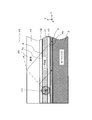
- FIG. 3 is an explanatory diagram showing the emission and scattering states of spontaneously emitted light Ln in Embodiment 1 of the present invention, and shows an enlarged cross-sectional view taken along the line AA ′ in FIG.
- FIG. 3 the radiation state of spontaneous emission light Ln at one excited point is shown. Actually, however, the same spontaneous emission light Ln is emitted at all locations in the excited laser medium 5. Occurs.
- the component in the direction of the laser beam axis 6 (z-axis direction) of the spontaneous emission light Ln radiated in the laser medium 5 becomes the seed beam of laser oscillation, which is amplified by the laser resonator and laser oscillation light. Is obtained.
- part of the component (two-dot chain arrow) having an angle in the y-axis direction in the spontaneous emission light Ln is totally reflected by the first cladding 4a, but passes through the second cladding 4b.
- a component having an angle in the y-axis direction passes through the first cladding 4a, further passes through the substrate 22, and leaks outside the solid-state laser element of the planar waveguide laser device.
- the refractive index n4 of the substrate 22 is higher than the refractive index n2 of the first cladding 4a. Therefore, a part of the transmitted light (dotted arrow) is reflected by Fresnel reflection.
- the laser medium 5 is Nd: YVO4
- the substrate 22 is YVO4 from which the active medium Nd is removed
- the refractive index n4 is 2.17 with respect to the c-axis direction.
- SiO2 is used for the first cladding 4a
- the refractive index n2 is 1.45. Therefore, 7% Fresnel reflection occurs between the first cladding 4a and the substrate 22 in the case of normal incidence. . At this time, the Fresnel reflection at the interface between the upper surface of the substrate 22 and the air is 13.4%.
- the incident angle when the incident angle is not vertical, there are a polarization direction in which the reflectivity increases and a polarization direction in which the reflectivity decreases according to the polarization direction with respect to the reflection surface.
- the light (dotted arrow) reflected at the boundary between the first clad 4 a and the substrate 22 passes through the second clad 4 b and is scattered or absorbed by the bonding agent 3 or the heat sink 2.
- part (dotted arrow) is also reflected between the substrate 22 and the air layer by Fresnel reflection, and the reflected light passes through the first cladding 4a, the laser medium 5 and the second cladding 4b, Scattered or absorbed by the bonding agent 3 or the heat sink 2.
- the light passing through the laser medium 5 and the light scattered by the bonding agent 3 or the heat sink 2 are amplified by passing through the laser medium 5 again, and the stored energy is extracted.
- the laser gain of the laser beam decreases, resulting in a low-efficiency and low-power laser output.
- the refractive indexes n2 and n4 of the first cladding 4a and the substrate 22 are set as in the above-described conditional expression (1). And Fresnel reflection at the boundary surface between the upper surface of the substrate 22 and air can be suppressed.
- the laser medium 5 is Nd: YVO4 and the first cladding 4a is SiO2
- a glass material that satisfies the conditional expression (1) can be used as the substrate 22.
- Fresnel reflection can be reduced to about 1% when perpendicular incidence occurs at the boundary surface between the first cladding 4a and the substrate 22.
- the Fresnel reflection component at the interface between the substrate 22 and air is reduced to about 4%.
- the relationship between the refractive index n2 of the first cladding 4a and the refractive index n4 of the substrate 22 may be set as in the following conditional expression (2).
- the refractive index n3 of the second cladding 4b is desirably set to a value lower than the refractive index n2 of the first cladding 4a.
- the refractive index of Ta2O5 is about 2.08, which is lower than the extraordinary refractive index of 2.16 of Nd: YVO4, and Nd: YVO4. Therefore, linearly polarized light in the direction in which the extraordinary refractive index can be obtained is obtained.
- laser oscillation can be performed at various wavelengths at which gain is generated in the laser medium 5.
- laser oscillation in 1 ⁇ m band, 0.9 ⁇ m band, and 1.3 ⁇ m band is possible.
- the dielectric multilayer film on the end face is designed to reflect or transmit a desired wavelength.
- the ratio of the spontaneous emission light Ln coupled to the waveguide can be reduced.
- a wave laser beam L1 is obtained.
- the nonlinear material 7 by converting the wavelength of the fundamental laser beam L1 into the second harmonic laser beam L2, a blue laser of 0.4 ⁇ m band can be obtained.
- Example 2 Although not particularly mentioned in the first embodiment (FIGS. 1 to 3), as shown in FIG. 4, the direction perpendicular to the x-axis (substantially parallel to the laser optical axis 6 (z-axis direction)).
- the configurations of the conditional expressions (1) and (2) may be applied.
- FIG. 4 is an explanatory diagram showing the emission and scattering states of spontaneous emission light Ln in Embodiment 2 of the present invention, where conditional expressions (1) and (2) are applied to a solid-state laser element on which a roughened surface 16 is formed. Is shown.
- the laser beam diameter is expanded in the direction perpendicular to the laser optical axis 6 (z-axis direction) (x-axis direction) within the flat plate surface, or the semiconductor laser 1 It is known that high output can be realized by using a multi-emitter LD in which a plurality of light emitting points are arranged.
- the component (broken line arrow) of the spontaneous emission light Ln generated in the laser medium 5 and traveling in the x-axis direction becomes scattered light (one-dot chain arrow) when irradiated on the rough surface 16.
- the spontaneously emitted light Ln (one-dot chain arrow) scattered by the rough surface 16 has various angle components, and a part of the components having an angle in the y-axis direction (dotted arrow) is the first cladding 4a. Is totally reflected, but passes through the second cladding 4b.
- the component having an angle in the y-axis direction passes through the first cladding 4a, further passes through the substrate 22, and leaks outside the solid-state laser element of the planar waveguide laser device.
- the refractive index n4 of the substrate 22 is higher than the refractive index n2 of the first cladding 4a. Therefore, a part of the transmitted light (dotted arrow) is reflected by Fresnel reflection. Similarly, part (dotted arrow) is also reflected between the substrate 22 and the air layer by Fresnel reflection.
- the stored energy is extracted by the parasitic amplification caused by the spontaneous emission light Ln passing through the laser medium 5 again, so that the laser gain in the direction of the laser optical axis 6 is reduced, and the laser with low efficiency and low output is obtained.
- the gain of the laser medium 5 in the vicinity of the roughened surface 16 may be reduced by parasitic amplification caused by the scattered light (one-dot chain line) on the roughened surface 16.
- FIG. 5 is an explanatory diagram showing the general dependence of the laser output on the excitation LD emitter.
- the excitation LD when 15 emitters are arrayed in the x-axis direction. It shows emitter dependency.
- the gain of the laser medium 5 near the roughening surface 16 decreases, so that the laser output is low at the emitter close to the roughening surface 16.
- the refractive indexes n2 and n4 of the first cladding 4a and the substrate 22 are set as in the conditional expressions (1) and (2) described above, the first cladding 4a Fresnel reflection at the boundary surface between 4a and the substrate 22 and the boundary surface between the upper surface of the substrate 22 and air can be suppressed.
- FIG. 6 is an explanatory diagram showing the emitter position dependence of the laser output in the second embodiment of the present invention, and shows the emitter position dependence when 15 emitter LD excitations are performed.
- the spontaneous emission light Ln passing through the laser medium 5 again is reduced as described above.
- the gain in the direction of the laser optical axis 6 is improved, and there is an effect that high-efficiency and high-power laser light can be obtained.
- Example 3 In the second embodiment (FIG. 4), the case where the present invention is applied to a solid-state laser element having a rough surface 16 perpendicular to the side end face is shown. However, as shown in FIG. 7, an inclined rough surface (rough inclined surface) is used. You may apply the structure of said conditional expression (1), (2) to the solid-state laser element which has 16A.
- FIG. 7 is an explanatory view showing the emission and scattering states of spontaneous emission light Ln in Embodiment 3 of the present invention, and conditional expressions (1) and (2) are applied to the solid-state laser element on which the rough inclined surface 16A is formed. Shows the case.
- FIG. 7 the same components as those described above (see FIG. 4) are denoted by the same reference numerals as those described above, and detailed description thereof is omitted.
- the overall configuration of the planar waveguide laser device according to Embodiment 3 of the present invention is as shown in FIGS.
- the gain in the x-axis direction is increased. Increases and parasitic oscillation and parasitic amplification easily occur. Therefore, it is desirable to form a rough inclined surface 16A having an angle of about 45 ° on the side end surface of the solid-state laser element that is substantially parallel to the laser optical axis 6, as shown in FIG.
- the main axis (solid arrow) of the scattered light (one-dot chain arrow) of the naturally radiated light Ln (broken arrow) on the rough inclined surface 16A is applied to the substrate 22. It can be directed in the vertical direction (y-axis direction).
- the reflected light of the waveguide component that can be reflected by the first cladding 4a or the second cladding 4b can be reduced, and the main component of the scattered light (dashed line arrow) can be released to the substrate 22 side.
- Parasitic amplification using light scattered by the rough inclined surface 16A as a seed light source can be suppressed.
- the refractive indexes n2 and n4 of the first cladding 4a and the substrate 22 are set as in the conditional expressions (1) and (2) described above, the first cladding 4a Fresnel reflection at the boundary surface between 4a and the substrate 22 and the boundary surface between the upper surface of the substrate 22 and air can be suppressed.
- the spontaneously emitted light Ln passing through the laser medium 5 again is similar to the above. Since the parasitic amplification is reduced and unintended parasitic amplification is suppressed, the gain in the direction of the laser optical axis 6 is improved, and there is an effect that high-efficiency and high-power laser light can be obtained.
- Example 4 In the third embodiment (FIG. 7), the case where the present invention is applied to a solid-state laser element having a rough and inclined surface 16A on the side end face is shown, but as shown in FIG. 8, it has an inclined mirror surface (inclined mirror surface) 16B. You may apply the structure of said conditional expression (1), (2) to a solid-state laser element.
- FIG. 8 is an explanatory diagram showing the emission and reflection state of spontaneously emitted light Ln in Embodiment 4 of the present invention, where conditional expressions (1) and (2) are applied to a solid-state laser element on which the inclined mirror surface 16B is formed. Is shown.
- FIG. 8 the same components as those described above (see FIG. 7) are denoted by the same reference numerals as those described above, and detailed description thereof is omitted.
- the overall configuration of the planar waveguide laser device according to Embodiment 4 of the present invention is as shown in FIGS.
- an inclined mirror surface 16B is formed on the side end face of the solid-state laser element that is substantially parallel to the laser optical axis 6. As shown in FIG. 8, by forming the inclined mirror surface 16B on the side end surface, no scattered light is generated on the inclined mirror surface 16B, and only the reflected light of the laser optical axis component (solid arrow) reflected to the substrate 22 side is reflected. Will occur.
- the refractive indexes n2 and n4 of the first cladding 4a and the substrate 22 are set as in the conditional expressions (1) and (2) described above, the first cladding 4a Fresnel reflection at the boundary surface between 4a and the substrate 22 and the boundary surface between the upper surface of the substrate 22 and air can be suppressed.
- the spontaneous emission light Ln passing through the laser medium 5 again is reduced as described above.
- the gain in the direction of the laser optical axis 6 is improved, and there is an effect that high-efficiency and high-power laser light can be obtained.
- parasitic amplification due to Fresnel reflection can be reduced, and since scattering due to reflection at the inclined mirror surface 16B does not occur, components that recombine directly with the waveguide due to scattering components deviated from the main axis of reflection are removed. Therefore, the ratio of spontaneous emission light recombined with the waveguide can be greatly reduced, unintended parasitic amplification is further suppressed, and laser light with higher efficiency and higher output can be obtained.
- Example 5 In Examples 1 to 4 (FIGS. 1 to 8), the specific use of the planar waveguide laser device was not mentioned. For example, as shown in FIG. 9, a laser that functions as a display device is used. You may apply to TV (television) 25. FIG. 9
- FIG. 9 is a block diagram showing a laser TV 25 using a planar waveguide laser device according to Embodiment 5 of the present invention. As a representative example, the configuration of a laser TV using a wavelength conversion laser as a light source is shown.
- a laser TV 25 can be used for a rear projection TV, a front projection TV, a backlight of a liquid crystal TV, or another TV.
- a red light source 26, a green light source 27, a blue light source 28, and a light propagation A means 29, an optical system 30, and a screen 31 are included.
- Each of the red light source 26, the green light source 27, and the blue light source 28 is configured by the planar waveguide laser device according to the first to fourth embodiments.
- the laser beams emitted from the red light source 26, the green light source 27, and the blue light source 28 are combined via the light propagation means 29, then emitted to the optical system 30, and projected from the optical system 30 onto the screen 31.
- planar waveguide laser device as each of the light sources 26 to 28 of the laser TV 25, a display device having excellent color reproducibility, high luminance, high definition, high color gamut, and low power consumption is realized. be able to.
Landscapes
- Physics & Mathematics (AREA)
- Electromagnetism (AREA)
- Engineering & Computer Science (AREA)
- Plasma & Fusion (AREA)
- Optics & Photonics (AREA)
- Lasers (AREA)
Abstract
La présente invention a trait à un dispositif laser à transformation de longueur d'onde, qui peut acquérir un faisceau laser d'onde fondamentale à rendement élevé et permettant d'effectuer une conversion harmonique secondaire de grande efficacité en supprimant une oscillation parasite et une extraction d'énergie par l'amplification d'une lumière émise naturellement vers un axe autre qu'un axe optique laser, et à un écran utilisant le dispositif laser à transformation de longueur d'onde. L'écran comprend un support laser plan (5) s'étendant dans une direction horizontale, une diode laser (1) disposée à proximité une surface d'extrémité incidente (5a), permettant de recevoir une lumière an excitée (L), un premier revêtement (4a) articulé sur la surface supérieure du support laser (5), un second revêtement (4b) revêtement la surface inférieure du support laser (5), et un substrat (22) articulé sur la surface supérieure du premier revêtement (4a). Le substrat (22) a un indice de réfraction (n4) défini en fonction de l'indice de réfraction (n2) du premier revêtement (4a) de sorte que l'indice de réfraction (n4) puisse satisfaire les relations suivantes : n2 – 0,1 < n4 < n2 + 0,1 de manière à être compris entre -0,1 et +0,1.
Priority Applications (2)
| Application Number | Priority Date | Filing Date | Title |
|---|---|---|---|
| PCT/JP2009/061208 WO2010146706A1 (fr) | 2009-06-19 | 2009-06-19 | Dispositif laser à guide d'ondes plan et écran utilisant le dispositif laser |
| JP2011519383A JP5389169B2 (ja) | 2009-06-19 | 2009-06-19 | 平面導波路型レーザ装置およびそれを用いたディスプレイ装置 |
Applications Claiming Priority (1)
| Application Number | Priority Date | Filing Date | Title |
|---|---|---|---|
| PCT/JP2009/061208 WO2010146706A1 (fr) | 2009-06-19 | 2009-06-19 | Dispositif laser à guide d'ondes plan et écran utilisant le dispositif laser |
Publications (1)
| Publication Number | Publication Date |
|---|---|
| WO2010146706A1 true WO2010146706A1 (fr) | 2010-12-23 |
Family
ID=43356044
Family Applications (1)
| Application Number | Title | Priority Date | Filing Date |
|---|---|---|---|
| PCT/JP2009/061208 Ceased WO2010146706A1 (fr) | 2009-06-19 | 2009-06-19 | Dispositif laser à guide d'ondes plan et écran utilisant le dispositif laser |
Country Status (2)
| Country | Link |
|---|---|
| JP (1) | JP5389169B2 (fr) |
| WO (1) | WO2010146706A1 (fr) |
Cited By (6)
| Publication number | Priority date | Publication date | Assignee | Title |
|---|---|---|---|---|
| JP2012146902A (ja) * | 2011-01-14 | 2012-08-02 | Mitsubishi Electric Corp | 平面導波路型レーザ装置およびその製造方法 |
| JP2012248609A (ja) * | 2011-05-26 | 2012-12-13 | Mitsubishi Electric Corp | 平面導波路型レーザ装置 |
| JP2013038096A (ja) * | 2011-08-03 | 2013-02-21 | Mitsubishi Electric Corp | 平面導波路型レーザ装置 |
| WO2014087468A1 (fr) * | 2012-12-03 | 2014-06-12 | 三菱電機株式会社 | Module d'excitation laser à guide d'ondes plan et dispositif laser de conversion de longueur d'onde à guide d'ondes plan |
| EP2782196A4 (fr) * | 2011-11-16 | 2015-09-02 | Mitsubishi Electric Corp | Laser à l'état solide à excitation de laser à semi-conducteur |
| JP2020141144A (ja) * | 2016-02-11 | 2020-09-03 | レイセオン カンパニー | 高出力レーザシステム用の強化された支持及び/又は冷却機構を備えた平面導波路 |
Citations (2)
| Publication number | Priority date | Publication date | Assignee | Title |
|---|---|---|---|---|
| JPH0968619A (ja) * | 1995-06-19 | 1997-03-11 | Nippon Telegr & Teleph Corp <Ntt> | 光導波路 |
| WO2009028078A1 (fr) * | 2007-08-30 | 2009-03-05 | Mitsubishi Electric Corporation | Élément laser solide |
-
2009
- 2009-06-19 WO PCT/JP2009/061208 patent/WO2010146706A1/fr not_active Ceased
- 2009-06-19 JP JP2011519383A patent/JP5389169B2/ja not_active Expired - Fee Related
Patent Citations (2)
| Publication number | Priority date | Publication date | Assignee | Title |
|---|---|---|---|---|
| JPH0968619A (ja) * | 1995-06-19 | 1997-03-11 | Nippon Telegr & Teleph Corp <Ntt> | 光導波路 |
| WO2009028078A1 (fr) * | 2007-08-30 | 2009-03-05 | Mitsubishi Electric Corporation | Élément laser solide |
Non-Patent Citations (1)
| Title |
|---|
| MACKENZIE, J.I. ET AL.: "Multi-watt, high efficiency, diffraction-limited Nd:YAG planar waveguide laser", IEEE JOURNAL OF QUANTUM ELECTRONICS, vol. 39, no. ISS.3, March 2003 (2003-03-01), pages 493 - 500, XP001175584, DOI: doi:10.1109/JQE.2002.808158 * |
Cited By (9)
| Publication number | Priority date | Publication date | Assignee | Title |
|---|---|---|---|---|
| JP2012146902A (ja) * | 2011-01-14 | 2012-08-02 | Mitsubishi Electric Corp | 平面導波路型レーザ装置およびその製造方法 |
| JP2012248609A (ja) * | 2011-05-26 | 2012-12-13 | Mitsubishi Electric Corp | 平面導波路型レーザ装置 |
| JP2013038096A (ja) * | 2011-08-03 | 2013-02-21 | Mitsubishi Electric Corp | 平面導波路型レーザ装置 |
| EP2782196A4 (fr) * | 2011-11-16 | 2015-09-02 | Mitsubishi Electric Corp | Laser à l'état solide à excitation de laser à semi-conducteur |
| WO2014087468A1 (fr) * | 2012-12-03 | 2014-06-12 | 三菱電機株式会社 | Module d'excitation laser à guide d'ondes plan et dispositif laser de conversion de longueur d'onde à guide d'ondes plan |
| US9312655B2 (en) | 2012-12-03 | 2016-04-12 | Mitsubishi Electric Corporation | Planar waveguide laser pumping module and planar waveguide wavelength conversion laser device |
| JPWO2014087468A1 (ja) * | 2012-12-03 | 2017-01-05 | 三菱電機株式会社 | 平面導波路型レーザ励起モジュールおよび平面導波路型波長変換レーザ装置 |
| JP2020141144A (ja) * | 2016-02-11 | 2020-09-03 | レイセオン カンパニー | 高出力レーザシステム用の強化された支持及び/又は冷却機構を備えた平面導波路 |
| JP6999740B2 (ja) | 2016-02-11 | 2022-01-19 | レイセオン カンパニー | 高出力レーザシステム用の強化された支持及び/又は冷却機構を備えた平面導波路 |
Also Published As
| Publication number | Publication date |
|---|---|
| JP5389169B2 (ja) | 2014-01-15 |
| JPWO2010146706A1 (ja) | 2012-11-29 |
Similar Documents
| Publication | Publication Date | Title |
|---|---|---|
| JP4392024B2 (ja) | モード制御導波路型レーザ装置 | |
| JP5389055B2 (ja) | 平面導波路型レーザおよびディスプレイ装置 | |
| US8068525B2 (en) | Solid-state laser element | |
| JP5389169B2 (ja) | 平面導波路型レーザ装置およびそれを用いたディスプレイ装置 | |
| JP5208118B2 (ja) | 固体レーザ素子 | |
| US9312655B2 (en) | Planar waveguide laser pumping module and planar waveguide wavelength conversion laser device | |
| WO2011027471A1 (fr) | Module d'excitation de laser solide pour laser à guide d'ondes plat | |
| JP5645753B2 (ja) | 平面導波路型レーザ装置 | |
| JP5247795B2 (ja) | 光モジュール | |
| US7769060B1 (en) | Laser light source, and display device using the same | |
| WO2011027579A1 (fr) | Appareil laser à guide d'ondes plan | |
| CN107112723B (zh) | 阵列型波长转换激光装置 | |
| CN107851953B (zh) | 平面波导型激光装置 | |
| CN104205528B (zh) | 激光器装置 | |
| US20080020083A1 (en) | Method for joining optical members, structure for integrating optical members and laser oscillation device |
Legal Events
| Date | Code | Title | Description |
|---|---|---|---|
| 121 | Ep: the epo has been informed by wipo that ep was designated in this application |
Ref document number: 09846199 Country of ref document: EP Kind code of ref document: A1 |
|
| ENP | Entry into the national phase |
Ref document number: 2011519383 Country of ref document: JP Kind code of ref document: A |
|
| NENP | Non-entry into the national phase |
Ref country code: DE |
|
| 122 | Ep: pct application non-entry in european phase |
Ref document number: 09846199 Country of ref document: EP Kind code of ref document: A1 |