WO2011027471A1 - Module d'excitation de laser solide pour laser à guide d'ondes plat - Google Patents
Module d'excitation de laser solide pour laser à guide d'ondes plat Download PDFInfo
- Publication number
- WO2011027471A1 WO2011027471A1 PCT/JP2009/065577 JP2009065577W WO2011027471A1 WO 2011027471 A1 WO2011027471 A1 WO 2011027471A1 JP 2009065577 W JP2009065577 W JP 2009065577W WO 2011027471 A1 WO2011027471 A1 WO 2011027471A1
- Authority
- WO
- WIPO (PCT)
- Prior art keywords
- laser
- light
- pair
- solid
- medium
- Prior art date
- Legal status (The legal status is an assumption and is not a legal conclusion. Google has not performed a legal analysis and makes no representation as to the accuracy of the status listed.)
- Ceased
Links
Images









Classifications
-
- H—ELECTRICITY
- H01—ELECTRIC ELEMENTS
- H01S—DEVICES USING THE PROCESS OF LIGHT AMPLIFICATION BY STIMULATED EMISSION OF RADIATION [LASER] TO AMPLIFY OR GENERATE LIGHT; DEVICES USING STIMULATED EMISSION OF ELECTROMAGNETIC RADIATION IN WAVE RANGES OTHER THAN OPTICAL
- H01S3/00—Lasers, i.e. devices using stimulated emission of electromagnetic radiation in the infrared, visible or ultraviolet wave range
- H01S3/09—Processes or apparatus for excitation, e.g. pumping
- H01S3/091—Processes or apparatus for excitation, e.g. pumping using optical pumping
- H01S3/094—Processes or apparatus for excitation, e.g. pumping using optical pumping by coherent light
- H01S3/0941—Processes or apparatus for excitation, e.g. pumping using optical pumping by coherent light of a laser diode
-
- H—ELECTRICITY
- H01—ELECTRIC ELEMENTS
- H01S—DEVICES USING THE PROCESS OF LIGHT AMPLIFICATION BY STIMULATED EMISSION OF RADIATION [LASER] TO AMPLIFY OR GENERATE LIGHT; DEVICES USING STIMULATED EMISSION OF ELECTROMAGNETIC RADIATION IN WAVE RANGES OTHER THAN OPTICAL
- H01S3/00—Lasers, i.e. devices using stimulated emission of electromagnetic radiation in the infrared, visible or ultraviolet wave range
- H01S3/05—Construction or shape of optical resonators; Accommodation of active medium therein; Shape of active medium
- H01S3/06—Construction or shape of active medium
- H01S3/0602—Crystal lasers or glass lasers
- H01S3/0606—Crystal lasers or glass lasers with polygonal cross-section, e.g. slab, prism
-
- H—ELECTRICITY
- H01—ELECTRIC ELEMENTS
- H01S—DEVICES USING THE PROCESS OF LIGHT AMPLIFICATION BY STIMULATED EMISSION OF RADIATION [LASER] TO AMPLIFY OR GENERATE LIGHT; DEVICES USING STIMULATED EMISSION OF ELECTROMAGNETIC RADIATION IN WAVE RANGES OTHER THAN OPTICAL
- H01S3/00—Lasers, i.e. devices using stimulated emission of electromagnetic radiation in the infrared, visible or ultraviolet wave range
- H01S3/05—Construction or shape of optical resonators; Accommodation of active medium therein; Shape of active medium
- H01S3/06—Construction or shape of active medium
- H01S3/0602—Crystal lasers or glass lasers
- H01S3/0612—Non-homogeneous structure
-
- H—ELECTRICITY
- H01—ELECTRIC ELEMENTS
- H01S—DEVICES USING THE PROCESS OF LIGHT AMPLIFICATION BY STIMULATED EMISSION OF RADIATION [LASER] TO AMPLIFY OR GENERATE LIGHT; DEVICES USING STIMULATED EMISSION OF ELECTROMAGNETIC RADIATION IN WAVE RANGES OTHER THAN OPTICAL
- H01S3/00—Lasers, i.e. devices using stimulated emission of electromagnetic radiation in the infrared, visible or ultraviolet wave range
- H01S3/05—Construction or shape of optical resonators; Accommodation of active medium therein; Shape of active medium
- H01S3/06—Construction or shape of active medium
- H01S3/0619—Coatings, e.g. AR, HR, passivation layer
- H01S3/0621—Coatings on the end-faces, e.g. input/output surfaces of the laser light
- H01S3/0623—Antireflective [AR]
-
- H—ELECTRICITY
- H01—ELECTRIC ELEMENTS
- H01S—DEVICES USING THE PROCESS OF LIGHT AMPLIFICATION BY STIMULATED EMISSION OF RADIATION [LASER] TO AMPLIFY OR GENERATE LIGHT; DEVICES USING STIMULATED EMISSION OF ELECTROMAGNETIC RADIATION IN WAVE RANGES OTHER THAN OPTICAL
- H01S3/00—Lasers, i.e. devices using stimulated emission of electromagnetic radiation in the infrared, visible or ultraviolet wave range
- H01S3/05—Construction or shape of optical resonators; Accommodation of active medium therein; Shape of active medium
- H01S3/06—Construction or shape of active medium
- H01S3/0619—Coatings, e.g. AR, HR, passivation layer
- H01S3/0625—Coatings on surfaces other than the end-faces
-
- H—ELECTRICITY
- H01—ELECTRIC ELEMENTS
- H01S—DEVICES USING THE PROCESS OF LIGHT AMPLIFICATION BY STIMULATED EMISSION OF RADIATION [LASER] TO AMPLIFY OR GENERATE LIGHT; DEVICES USING STIMULATED EMISSION OF ELECTROMAGNETIC RADIATION IN WAVE RANGES OTHER THAN OPTICAL
- H01S3/00—Lasers, i.e. devices using stimulated emission of electromagnetic radiation in the infrared, visible or ultraviolet wave range
- H01S3/02—Constructional details
- H01S3/04—Arrangements for thermal management
- H01S3/0407—Liquid cooling, e.g. by water
-
- H—ELECTRICITY
- H01—ELECTRIC ELEMENTS
- H01S—DEVICES USING THE PROCESS OF LIGHT AMPLIFICATION BY STIMULATED EMISSION OF RADIATION [LASER] TO AMPLIFY OR GENERATE LIGHT; DEVICES USING STIMULATED EMISSION OF ELECTROMAGNETIC RADIATION IN WAVE RANGES OTHER THAN OPTICAL
- H01S3/00—Lasers, i.e. devices using stimulated emission of electromagnetic radiation in the infrared, visible or ultraviolet wave range
- H01S3/02—Constructional details
- H01S3/04—Arrangements for thermal management
- H01S3/042—Arrangements for thermal management for solid state lasers
-
- H—ELECTRICITY
- H01—ELECTRIC ELEMENTS
- H01S—DEVICES USING THE PROCESS OF LIGHT AMPLIFICATION BY STIMULATED EMISSION OF RADIATION [LASER] TO AMPLIFY OR GENERATE LIGHT; DEVICES USING STIMULATED EMISSION OF ELECTROMAGNETIC RADIATION IN WAVE RANGES OTHER THAN OPTICAL
- H01S3/00—Lasers, i.e. devices using stimulated emission of electromagnetic radiation in the infrared, visible or ultraviolet wave range
- H01S3/05—Construction or shape of optical resonators; Accommodation of active medium therein; Shape of active medium
- H01S3/06—Construction or shape of active medium
- H01S3/0602—Crystal lasers or glass lasers
- H01S3/0615—Shape of end-face
-
- H—ELECTRICITY
- H01—ELECTRIC ELEMENTS
- H01S—DEVICES USING THE PROCESS OF LIGHT AMPLIFICATION BY STIMULATED EMISSION OF RADIATION [LASER] TO AMPLIFY OR GENERATE LIGHT; DEVICES USING STIMULATED EMISSION OF ELECTROMAGNETIC RADIATION IN WAVE RANGES OTHER THAN OPTICAL
- H01S3/00—Lasers, i.e. devices using stimulated emission of electromagnetic radiation in the infrared, visible or ultraviolet wave range
- H01S3/05—Construction or shape of optical resonators; Accommodation of active medium therein; Shape of active medium
- H01S3/06—Construction or shape of active medium
- H01S3/063—Waveguide lasers, i.e. whereby the dimensions of the waveguide are of the order of the light wavelength
- H01S3/0632—Thin film lasers in which light propagates in the plane of the thin film
-
- H—ELECTRICITY
- H01—ELECTRIC ELEMENTS
- H01S—DEVICES USING THE PROCESS OF LIGHT AMPLIFICATION BY STIMULATED EMISSION OF RADIATION [LASER] TO AMPLIFY OR GENERATE LIGHT; DEVICES USING STIMULATED EMISSION OF ELECTROMAGNETIC RADIATION IN WAVE RANGES OTHER THAN OPTICAL
- H01S3/00—Lasers, i.e. devices using stimulated emission of electromagnetic radiation in the infrared, visible or ultraviolet wave range
- H01S3/05—Construction or shape of optical resonators; Accommodation of active medium therein; Shape of active medium
- H01S3/08—Construction or shape of optical resonators or components thereof
- H01S3/08072—Thermal lensing or thermally induced birefringence; Compensation thereof
-
- H—ELECTRICITY
- H01—ELECTRIC ELEMENTS
- H01S—DEVICES USING THE PROCESS OF LIGHT AMPLIFICATION BY STIMULATED EMISSION OF RADIATION [LASER] TO AMPLIFY OR GENERATE LIGHT; DEVICES USING STIMULATED EMISSION OF ELECTROMAGNETIC RADIATION IN WAVE RANGES OTHER THAN OPTICAL
- H01S3/00—Lasers, i.e. devices using stimulated emission of electromagnetic radiation in the infrared, visible or ultraviolet wave range
- H01S3/09—Processes or apparatus for excitation, e.g. pumping
- H01S3/091—Processes or apparatus for excitation, e.g. pumping using optical pumping
- H01S3/094—Processes or apparatus for excitation, e.g. pumping using optical pumping by coherent light
- H01S3/094049—Guiding of the pump light
Definitions
- planar waveguide type laser apparatus containing the solid-state laser excitation module by Embodiment 5 of this invention. It is a top view of the planar waveguide type laser apparatus containing the solid-state laser excitation module by Embodiment 6 of this invention. It is an enlarged view of the area
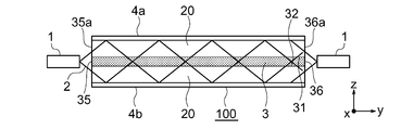
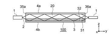
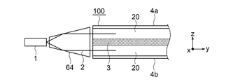
- the clads 4a and 4b shown in FIG. 2 have a refractive index smaller than that of the laser medium 3, and are respectively joined to main surfaces 31 and 32 parallel to the xy plane of the laser medium 3.
- the claddings 4a and 4b are configured by, for example, depositing a film made of an optical material as a raw material or optically bonding the optical material to the laser medium 3 by optical contact or diffusion bonding.
- the clads 4a and 4b may be bonded to a substrate (not shown). Further, the substrate may be bonded to a heat sink (not shown). The substrate and the heat sink may be on one side of the xy plane of the laser medium 3 or may be bonded to both sides of the two opposing surfaces.
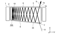
- the semiconductor lasers 1 on both sides are arranged close to the end faces 35 and 36 of the laser medium 3, and although not shown, a cooling heat sink is joined as necessary.
- the size of the semiconductor laser 1 in the x-axis direction is substantially equal to the size of the laser medium 3 in the x-axis direction, and pumping light is output substantially uniformly in the x-axis direction.
- the semiconductor laser 1 outputs excitation light 2.
- the semiconductor laser 1 that outputs the excitation light 2 may be a multi-emitter semiconductor laser in which a plurality of active layers are arranged in the x-axis direction.
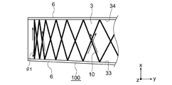
- the inclination angle ⁇ 1 between the side surfaces 33 and 34 depends on the length in the y direction in the xy plane of the laser medium 3, the width in the x direction, the beam width w of the laser light, the width of the antireflection film 7, and the like.
- the wrap efficiency is set to be high and the number of reflections is increased.
- such an angle is mainly set to an inclination angle ⁇ 1 ⁇ 2 degrees between the side surfaces 33 and 34.
- the present invention may be applied to a configuration in which the first clad 20 is disposed on the main surfaces 31 and 32 of the laser medium 3. Furthermore, you may arrange
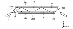
- the end surfaces 35a and 36a are inclined in the yz plane, the two end surfaces 35a and 36a facing each other and the laser medium 3, or between the end surfaces 35a and 36a and the first cladding 20, or the end surface 35a. , 36a and the second clad 4a, 4b can be eliminated by a parasitic oscillation path confined by total reflection.
- the end faces 35a and 36a are inclined, there is no parasitic oscillation in the yz plane and the parasitic amplification path length can be shortened. Therefore, energy extraction by parasitic oscillation and parasitic amplification can be performed during high output excitation. Since it is small and gain reduction is small, a high-power laser beam can be obtained.
- the laser medium 3 that reflects the excitation light 2 and the end face of the first cladding 20 are configured to be inclined in the yz plane. ing.
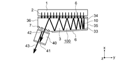
- the semiconductor laser 1 is disposed so as to introduce the excitation light 2 from the xy plane of the second cladding 4a (the outermost surface of the solid-state laser excitation module 100).
- the excitation light 2 introduced from the xy plane of the first cladding 4a is reflected by the inclined end surface.
- the reflected excitation light 2 propagates through the laser medium 3 and the second cladding 4a and is absorbed when passing through the laser medium 3 while propagating.
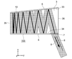
- FIG. 7 is a top view of a planar waveguide laser device including a solid-state laser excitation module according to Embodiment 6 of the present invention.
- FIG. 8 is an enlarged view of a region C indicated by a broken line in FIG. 7, and the scale in the y-axis direction is enlarged.
- the position of the side surface 33 attached with the inclination angle ⁇ 1 and the side surface 34 extending along the predetermined direction (y-axis direction) is interchanged as compared with the module 100 of FIG.
- An antireflection film 7 is provided on a part of the side on the 33 side where the side surface interval is wide.
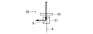
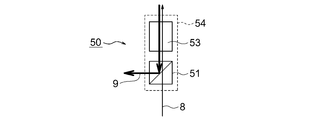
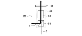
- the optical paths of the laser incident light 8 and the laser output light 9 are not the same. For this reason, since the laser incident light 8 and the laser output light 9 are spatially easily separated, it is not necessary to use a polarization separation means. For this reason, it is possible to reduce the number of components, particularly in a laser amplifier, and the reliability is also improved.
- the low-concentration laser medium 3 has a small number of active media that generate gain, the gain for the laser light is small.
- the laser light is reciprocally propagated between the side surfaces having the inclined side surfaces. Long propagation length. For this reason, even when the gain of the laser medium 3 per unit length is small, high-efficiency and high-power laser light can be obtained.
- FIG. 12 is a top view of a planar waveguide laser device including a solid-state laser excitation module according to Embodiment 10 of the present invention.
- the laser medium 3 is not rectangular, and the side surface 33 is angled in the xy plane with respect to the portion where the antireflection film 7 is provided and the portion where the total reflection film 6 is provided. Is (tilted).
- the portion provided with the antireflection film 7 on the side surface 33 is at an angle such that the laser incident light and the laser output light of the laser reflected light 10 having substantially the same optical path in the reciprocating optical path are perpendicular to the antireflection film 7. Is attached.
Landscapes
- Physics & Mathematics (AREA)
- Electromagnetism (AREA)
- Engineering & Computer Science (AREA)
- Plasma & Fusion (AREA)
- Optics & Photonics (AREA)
- Chemical & Material Sciences (AREA)
- Crystallography & Structural Chemistry (AREA)
- Lasers (AREA)
Abstract
L'invention concerne un module d'excitation de laser solide pour un dispositif laser à guide d'ondes plat, comprenant un milieu laser plat destiné à amplifier une lumière laser introduite tout en propageant celle-ci dans une direction suivant une paire de faces latérales (33 et 34) et en réfléchissant celle-ci entre les faces latérales. Une des faces (33) de la paire de faces latérales est inclinée selon un angle prédéterminé par rapport à une direction prédéterminée, si bien que son écartement par rapport à l'autre face (34) peut augmenter dans la direction prédéterminée. La lumière laser introduite dans le milieu laser à partir d'une partie prédéterminée de la paire de faces latérales, sur le côté où l'écartement entre les faces latérales est le plus grand, se propage dans le milieu laser tout en étant réfléchie par les faces latérales. Le faisceau laser fait demi-tour dans le milieu laser sur le côté où l'écartement entre les faces latérales est le plus petit, se propage à nouveau vers le côté où l'écartement entre les faces latérales est le plus grand, puis est délivré.
Priority Applications (3)
| Application Number | Priority Date | Filing Date | Title |
|---|---|---|---|
| PCT/JP2009/065577 WO2011027471A1 (fr) | 2009-09-07 | 2009-09-07 | Module d'excitation de laser solide pour laser à guide d'ondes plat |
| PCT/JP2010/050698 WO2011027579A1 (fr) | 2009-09-07 | 2010-01-21 | Appareil laser à guide d'ondes plan |
| PCT/JP2010/064703 WO2011027731A1 (fr) | 2009-09-07 | 2010-08-30 | Dispositif laser à guide d'ondes plan |
Applications Claiming Priority (1)
| Application Number | Priority Date | Filing Date | Title |
|---|---|---|---|
| PCT/JP2009/065577 WO2011027471A1 (fr) | 2009-09-07 | 2009-09-07 | Module d'excitation de laser solide pour laser à guide d'ondes plat |
Publications (1)
| Publication Number | Publication Date |
|---|---|
| WO2011027471A1 true WO2011027471A1 (fr) | 2011-03-10 |
Family
ID=43649033
Family Applications (1)
| Application Number | Title | Priority Date | Filing Date |
|---|---|---|---|
| PCT/JP2009/065577 Ceased WO2011027471A1 (fr) | 2009-09-07 | 2009-09-07 | Module d'excitation de laser solide pour laser à guide d'ondes plat |
Country Status (1)
| Country | Link |
|---|---|
| WO (1) | WO2011027471A1 (fr) |
Cited By (8)
| Publication number | Priority date | Publication date | Assignee | Title |
|---|---|---|---|---|
| JP2013219137A (ja) * | 2012-04-06 | 2013-10-24 | Mitsubishi Electric Corp | 平面導波路型レーザ装置 |
| JP2014096510A (ja) * | 2012-11-12 | 2014-05-22 | Mitsubishi Electric Corp | 光増幅器 |
| CN107167250A (zh) * | 2017-05-10 | 2017-09-15 | 太原理工大学 | 一种压电陶瓷微位移光干涉检测控制装置 |
| JP2018538688A (ja) * | 2015-11-25 | 2018-12-27 | レイセオン カンパニー | 高出力レーザシステム用の一体化ポンプ光ホモジナイザ及び信号インジェクタ |
| JP6811898B1 (ja) * | 2019-12-18 | 2021-01-13 | 三菱電機株式会社 | 平面導波路型増幅器およびレーザレーダ装置 |
| US11431145B2 (en) * | 2016-05-09 | 2022-08-30 | Deutsches Zentrum Fuer Luft- Und Raumfahrt E.V. | Solid-state laser gain medium with inclined reflective planes for pump and seed radiation confinement |
| CN116722435A (zh) * | 2023-07-07 | 2023-09-08 | 北京应用物理与计算数学研究所 | 多光束布里渊放大器件以及激光放大方法 |
| CN117317780A (zh) * | 2023-09-26 | 2023-12-29 | 中国科学院理化技术研究所 | 板条激光放大装置 |
Citations (7)
| Publication number | Priority date | Publication date | Assignee | Title |
|---|---|---|---|---|
| US3665335A (en) * | 1970-01-26 | 1972-05-23 | Gen Electric | Coolable slab laser |
| JP2002528900A (ja) * | 1998-10-16 | 2002-09-03 | コミツサリア タ レネルジー アトミーク | 光ポンピングされる平面導波路を備えた光増幅器および該光増幅器を用いたパワーレーザ |
| US20030063884A1 (en) * | 2001-01-04 | 2003-04-03 | Smith Duane D. | Power scalable optical systems for generating, transporting, and delivering high power, high quality, laser beams |
| WO2004114476A1 (fr) * | 2003-06-20 | 2004-12-29 | Mitsubishi Denki Kabushiki Kaisha | Module d'excitation a laser solide |
| WO2006001063A1 (fr) * | 2004-06-28 | 2006-01-05 | Mitsubishi Denki Kabushiki Kaisha | Module d’excitation d’un laser à solide |
| JP2006516817A (ja) * | 2003-01-28 | 2006-07-06 | ハイ キュー レーザー プロダクション ゲゼルシャフト ミット ベシュレンクテル ハフツング | レーザービームガイド用折返し装置 |
| JP2008522409A (ja) * | 2004-11-26 | 2008-06-26 | ジェフリー, ジー マンニ, | 高利得ダイオード励起レーザ増幅器 |
-
2009
- 2009-09-07 WO PCT/JP2009/065577 patent/WO2011027471A1/fr not_active Ceased
Patent Citations (7)
| Publication number | Priority date | Publication date | Assignee | Title |
|---|---|---|---|---|
| US3665335A (en) * | 1970-01-26 | 1972-05-23 | Gen Electric | Coolable slab laser |
| JP2002528900A (ja) * | 1998-10-16 | 2002-09-03 | コミツサリア タ レネルジー アトミーク | 光ポンピングされる平面導波路を備えた光増幅器および該光増幅器を用いたパワーレーザ |
| US20030063884A1 (en) * | 2001-01-04 | 2003-04-03 | Smith Duane D. | Power scalable optical systems for generating, transporting, and delivering high power, high quality, laser beams |
| JP2006516817A (ja) * | 2003-01-28 | 2006-07-06 | ハイ キュー レーザー プロダクション ゲゼルシャフト ミット ベシュレンクテル ハフツング | レーザービームガイド用折返し装置 |
| WO2004114476A1 (fr) * | 2003-06-20 | 2004-12-29 | Mitsubishi Denki Kabushiki Kaisha | Module d'excitation a laser solide |
| WO2006001063A1 (fr) * | 2004-06-28 | 2006-01-05 | Mitsubishi Denki Kabushiki Kaisha | Module d’excitation d’un laser à solide |
| JP2008522409A (ja) * | 2004-11-26 | 2008-06-26 | ジェフリー, ジー マンニ, | 高利得ダイオード励起レーザ増幅器 |
Cited By (10)
| Publication number | Priority date | Publication date | Assignee | Title |
|---|---|---|---|---|
| JP2013219137A (ja) * | 2012-04-06 | 2013-10-24 | Mitsubishi Electric Corp | 平面導波路型レーザ装置 |
| JP2014096510A (ja) * | 2012-11-12 | 2014-05-22 | Mitsubishi Electric Corp | 光増幅器 |
| JP2018538688A (ja) * | 2015-11-25 | 2018-12-27 | レイセオン カンパニー | 高出力レーザシステム用の一体化ポンプ光ホモジナイザ及び信号インジェクタ |
| US11431145B2 (en) * | 2016-05-09 | 2022-08-30 | Deutsches Zentrum Fuer Luft- Und Raumfahrt E.V. | Solid-state laser gain medium with inclined reflective planes for pump and seed radiation confinement |
| CN107167250A (zh) * | 2017-05-10 | 2017-09-15 | 太原理工大学 | 一种压电陶瓷微位移光干涉检测控制装置 |
| JP6811898B1 (ja) * | 2019-12-18 | 2021-01-13 | 三菱電機株式会社 | 平面導波路型増幅器およびレーザレーダ装置 |
| WO2021124471A1 (fr) * | 2019-12-18 | 2021-06-24 | 三菱電機株式会社 | Amplificateur à guide d'ondes planaire et dispositif radar laser |
| EP4064467A4 (fr) * | 2019-12-18 | 2022-11-23 | Mitsubishi Electric Corporation | Amplificateur à guide d'ondes planaire et dispositif radar laser |
| CN116722435A (zh) * | 2023-07-07 | 2023-09-08 | 北京应用物理与计算数学研究所 | 多光束布里渊放大器件以及激光放大方法 |
| CN117317780A (zh) * | 2023-09-26 | 2023-12-29 | 中国科学院理化技术研究所 | 板条激光放大装置 |
Similar Documents
| Publication | Publication Date | Title |
|---|---|---|
| US6785304B2 (en) | Waveguide device with mode control and pump light confinement and method of using same | |
| WO2011027731A1 (fr) | Dispositif laser à guide d'ondes plan | |
| JP4392024B2 (ja) | モード制御導波路型レーザ装置 | |
| JP4754020B2 (ja) | 平面導波路型レーザ装置 | |
| EP2475054A1 (fr) | Milieu actif à disques minces multiples à pompage colinéaire et son système de pompage | |
| US9312655B2 (en) | Planar waveguide laser pumping module and planar waveguide wavelength conversion laser device | |
| JP2000244042A (ja) | 光導波路並びにその光導波路を用いたレーザ発振器およびレーザ増幅器 | |
| US8705586B2 (en) | Solid-state laser element | |
| WO2010013546A1 (fr) | Dispositif laser à semi-conducteurs | |
| US20220294170A1 (en) | Planar waveguide amplifier and laser radar device | |
| JP4883503B2 (ja) | 多重光路の固体スラブレーザロッドまたは非線形光学結晶を用いたレーザ装置 | |
| US20110064112A1 (en) | Solid-state laser with waveguide pump path (z pump) | |
| WO2011027579A1 (fr) | Appareil laser à guide d'ondes plan | |
| US20080025362A1 (en) | Solid-State-Laser Pumping Module | |
| JP5389169B2 (ja) | 平面導波路型レーザ装置およびそれを用いたディスプレイ装置 | |
| JP5645753B2 (ja) | 平面導波路型レーザ装置 | |
| JP6124683B2 (ja) | 平面導波路型レーザ装置 | |
| JP4101838B2 (ja) | 固体レーザ励起モジュール及びレーザ発振器 | |
| JP2007110039A (ja) | 固体レーザ励起モジュール | |
| JP4402048B2 (ja) | 固体レーザ励起モジュール及びレーザ発振器 | |
| CN107851953B (zh) | 平面波导型激光装置 | |
| JP2000077750A (ja) | 固体レーザ装置 | |
| JP5987193B2 (ja) | 光増幅器 | |
| WO2016111361A1 (fr) | Dispositif laser à conversion de longueur d'onde du type à réseau | |
| JP2009182053A (ja) | レーザー装置 |
Legal Events
| Date | Code | Title | Description |
|---|---|---|---|
| 121 | Ep: the epo has been informed by wipo that ep was designated in this application |
Ref document number: 09849001 Country of ref document: EP Kind code of ref document: A1 |
|
| NENP | Non-entry into the national phase |
Ref country code: DE |
|
| 122 | Ep: pct application non-entry in european phase |
Ref document number: 09849001 Country of ref document: EP Kind code of ref document: A1 |
|
| NENP | Non-entry into the national phase |
Ref country code: JP |