WO2010150909A1 - 3相整流器 - Google Patents
3相整流器 Download PDFInfo
- Publication number
- WO2010150909A1 WO2010150909A1 PCT/JP2010/060976 JP2010060976W WO2010150909A1 WO 2010150909 A1 WO2010150909 A1 WO 2010150909A1 JP 2010060976 W JP2010060976 W JP 2010060976W WO 2010150909 A1 WO2010150909 A1 WO 2010150909A1
- Authority
- WO
- WIPO (PCT)
- Prior art keywords
- phase
- voltage
- circuit
- switching
- input
- Prior art date
- Legal status (The legal status is an assumption and is not a legal conclusion. Google has not performed a legal analysis and makes no representation as to the accuracy of the status listed.)
- Ceased
Links
Images











Classifications
-
- H—ELECTRICITY
- H02—GENERATION; CONVERSION OR DISTRIBUTION OF ELECTRIC POWER
- H02M—APPARATUS FOR CONVERSION BETWEEN AC AND AC, BETWEEN AC AND DC, OR BETWEEN DC AND DC, AND FOR USE WITH MAINS OR SIMILAR POWER SUPPLY SYSTEMS; CONVERSION OF DC OR AC INPUT POWER INTO SURGE OUTPUT POWER; CONTROL OR REGULATION THEREOF
- H02M7/00—Conversion of AC power input into DC power output; Conversion of DC power input into AC power output
- H02M7/02—Conversion of AC power input into DC power output without possibility of reversal
- H02M7/04—Conversion of AC power input into DC power output without possibility of reversal by static converters
- H02M7/12—Conversion of AC power input into DC power output without possibility of reversal by static converters using discharge tubes with control electrode or semiconductor devices with control electrode
- H02M7/21—Conversion of AC power input into DC power output without possibility of reversal by static converters using discharge tubes with control electrode or semiconductor devices with control electrode using devices of a triode or transistor type requiring continuous application of a control signal
- H02M7/217—Conversion of AC power input into DC power output without possibility of reversal by static converters using discharge tubes with control electrode or semiconductor devices with control electrode using devices of a triode or transistor type requiring continuous application of a control signal using semiconductor devices only
- H02M7/219—Conversion of AC power input into DC power output without possibility of reversal by static converters using discharge tubes with control electrode or semiconductor devices with control electrode using devices of a triode or transistor type requiring continuous application of a control signal using semiconductor devices only in a bridge configuration
-
- H—ELECTRICITY
- H02—GENERATION; CONVERSION OR DISTRIBUTION OF ELECTRIC POWER
- H02M—APPARATUS FOR CONVERSION BETWEEN AC AND AC, BETWEEN AC AND DC, OR BETWEEN DC AND DC, AND FOR USE WITH MAINS OR SIMILAR POWER SUPPLY SYSTEMS; CONVERSION OF DC OR AC INPUT POWER INTO SURGE OUTPUT POWER; CONTROL OR REGULATION THEREOF
- H02M1/00—Details of apparatus for conversion
- H02M1/42—Circuits or arrangements for compensating for or adjusting power factor in converters or inverters
- H02M1/4208—Arrangements for improving power factor of AC input
- H02M1/4216—Arrangements for improving power factor of AC input operating from a three-phase input voltage
-
- H—ELECTRICITY
- H02—GENERATION; CONVERSION OR DISTRIBUTION OF ELECTRIC POWER
- H02M—APPARATUS FOR CONVERSION BETWEEN AC AND AC, BETWEEN AC AND DC, OR BETWEEN DC AND DC, AND FOR USE WITH MAINS OR SIMILAR POWER SUPPLY SYSTEMS; CONVERSION OF DC OR AC INPUT POWER INTO SURGE OUTPUT POWER; CONTROL OR REGULATION THEREOF
- H02M7/00—Conversion of AC power input into DC power output; Conversion of DC power input into AC power output
- H02M7/02—Conversion of AC power input into DC power output without possibility of reversal
- H02M7/04—Conversion of AC power input into DC power output without possibility of reversal by static converters
- H02M7/06—Conversion of AC power input into DC power output without possibility of reversal by static converters using discharge tubes without control electrode or semiconductor devices without control electrode
-
- H—ELECTRICITY
- H02—GENERATION; CONVERSION OR DISTRIBUTION OF ELECTRIC POWER
- H02M—APPARATUS FOR CONVERSION BETWEEN AC AND AC, BETWEEN AC AND DC, OR BETWEEN DC AND DC, AND FOR USE WITH MAINS OR SIMILAR POWER SUPPLY SYSTEMS; CONVERSION OF DC OR AC INPUT POWER INTO SURGE OUTPUT POWER; CONTROL OR REGULATION THEREOF
- H02M1/00—Details of apparatus for conversion
- H02M1/0083—Converters characterised by their input or output configuration
- H02M1/0085—Partially controlled bridges
-
- Y—GENERAL TAGGING OF NEW TECHNOLOGICAL DEVELOPMENTS; GENERAL TAGGING OF CROSS-SECTIONAL TECHNOLOGIES SPANNING OVER SEVERAL SECTIONS OF THE IPC; TECHNICAL SUBJECTS COVERED BY FORMER USPC CROSS-REFERENCE ART COLLECTIONS [XRACs] AND DIGESTS
- Y02—TECHNOLOGIES OR APPLICATIONS FOR MITIGATION OR ADAPTATION AGAINST CLIMATE CHANGE
- Y02B—CLIMATE CHANGE MITIGATION TECHNOLOGIES RELATED TO BUILDINGS, e.g. HOUSING, HOUSE APPLIANCES OR RELATED END-USER APPLICATIONS
- Y02B70/00—Technologies for an efficient end-user side electric power management and consumption
- Y02B70/10—Technologies improving the efficiency by using switched-mode power supplies [SMPS], i.e. efficient power electronics conversion e.g. power factor correction or reduction of losses in power supplies or efficient standby modes
Definitions
- the present invention relates to a three-phase rectifier that converts three-phase AC power into DC power.
- a three-phase full-wave rectification method is generally used as a method for converting three-phase AC power to DC power.
- the potential of each phase may be an intermediate potential between the potentials of the other two phases in one cycle, and is twice in a 60 ° section width. Since it is a non-conducting section that does not flow, the input current has a waveform including a harmonic current. Further, the DC voltage has a pulsating waveform because the maximum voltage of the input line voltage is traced.
- a so-called passive method is a method of reducing the input non-conduction section and reducing the harmonic current.
- the so-called passive method is to connect a large-capacity reactor to the input, accumulate power, and discharge to the non-conduction section.
- a method is used to reduce.
- a so-called active method is a method in which a PFC circuit or a PWM rectifier circuit is configured using a semiconductor and the input non-conduction period is compensated with a small-capacity reactor. Is used.
- both passive and active methods are performed by connecting a large-capacitance capacitor to the DC side.
- the passive method requires power storage.
- a large-capacity reactor and capacitor are required for storing electric power, and therefore there is a problem that the circuit scale is increased in price and cost.
- Patent Documents 1 and 2 are known as current-type three-phase step-down rectifiers used for active systems other than the above.
- a current-type step-down converter is configured by a self-extinguishing switching element, and a DC voltage is smoothed and a high-frequency current is inserted by inserting a section in which a DC voltage is zero by all pulse OFF or a short-circuit pulse into a rectifier output.
- Patent Document 2 proposes reducing the size of this type of DC reactor.
- the reactor that absorbs the power supply frequency component and the capacitance of the capacitor have a power supply frequency (for example, There is a problem that a certain size corresponding to 50 Hz) is required.
- the present invention has been made in view of the above, and is a step-down three-phase rectifier capable of reducing DC voltage pulsation and input current harmonics even when a small-capacitance capacitor or reactor is used.
- the purpose is to provide.
- the present invention provides a three-phase rectifier that converts three-phase AC power supplied from a three-phase AC power source into DC power, and converts the three-phase AC power into DC power.
- the switching pattern of each phase has a predetermined switching cycle
- the control means is a maximum potential phase, an intermediate potential of the voltage of each phase of the three-phase power source. Detecting the phase and the minimum potential phase, and in the case of the maximum potential phase and the minimum potential phase, generates a switching pattern in which the time is proportional to the respective potentials, and at least one is ON in the switching cycle, In the case of an intermediate potential phase, it is desirable to generate a switching pattern that is always ON.
- control means divides into a plurality of modes according to the magnitude relationship of the voltages of each phase, generates a different switching pattern for each phase in each mode, and It is desirable that the same phase in all modes has the same regular pattern.
- the switching pattern of each phase has a predetermined switching period
- the control means introduces a period during which at least two phases are OFF within each switching period. It is desirable to do.
- control means insert a zero voltage into a one-phase switching pattern.
- a full-wave rectifier circuit that rectifies the three-phase AC power into DC power
- a bi-directional switch circuit for turning on / off the input of each phase from the three-phase AC power source to the full-wave rectifier circuit, and detecting a voltage of each phase of the three-phase AC power source to obtain a detected voltage of each phase
- a control means for generating a switching pattern of each phase for turning the bidirectional switch circuit on and off based on the generated switching pattern and controlling the switching of the bidirectional switch circuit based on the generated switching pattern.
- FIG. 1 is a diagram illustrating a configuration example of a power conversion device to which a step-down three-phase rectifier according to the present embodiment is applied.
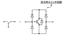
- FIG. 2 is a circuit diagram showing a configuration example of one phase switch of the bidirectional switch circuit.
- FIG. 3 is a block diagram illustrating a configuration example of the switching pattern generator.
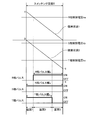
- FIG. 4 is a diagram showing waveform examples of sawtooth waves 1 and 2 used when a switching pattern is generated by a switching pattern generator.
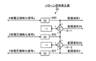
- FIG. 5 is a circuit diagram showing a configuration example of the pattern signal generator of FIG.
- FIG. 6 is a diagram illustrating a configuration example of the phase voltage discriminator of FIG.
- FIG. 7 is a diagram for explaining each section of the R-phase voltage, the S-phase voltage, and the T-phase voltage.
- FIG. 8 is a diagram illustrating an example of R, S, and T phase control voltages ka, kb, and kc, sawtooth waves 1 and 2, and R, S, and T phase pulses.
- FIG. 9 is a diagram showing simulation results of the DC voltage and DC current of the circuit of FIG.
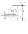
- FIG. 10 is a circuit diagram showing another configuration example of the bidirectional switch circuit.
- FIG. 11A is an example of R, S, and T phase control voltages ka, kb, and kc, sawtooth waves 1 and 2, and R, S, and T phase pulses in the first embodiment in modes I and II.
- FIG. 11-2 is an example of R, S, T phase control voltages ka, kb, kc, sawtooth waves 1, 2 and R, S, T phase pulses in the first embodiment in modes III and IV.
- FIG. FIG. 11C is an example of R, S, T phase control voltages ka, kb, kc, sawtooth waves 1 and 2, and R, S, T phase pulses in the first embodiment in modes V and VI.
- FIG. FIG. 12 is a block diagram illustrating an example of a switching pattern generator according to the second embodiment.
- FIG. 13 is a diagram illustrating waveform examples of the sawtooth waves 1 and 2 generated by the sawtooth wave generator.
- FIG. 14 is a diagram illustrating a configuration example of a phase voltage discriminator.
- FIG. 15 is a diagram illustrating a configuration example of the pattern signal generator.
- FIG. 16 is a diagram illustrating an example of a modulation waveform, a sawtooth wave, and R, S, and T phase pulses in modes II and V.
- FIG. 17 is a diagram illustrating an example of a modulation waveform, a sawtooth wave, and R, S, and T phase pulses in modes I and IV.
- FIG. 18 is a diagram illustrating an example of a modulation waveform, a sawtooth wave, and R, S, and T phase pulses in modes III and VI.
- FIG. 22 is a circuit diagram showing another configuration example of the bidirectional switch circuit.
- FIG. 1 is a diagram illustrating a configuration example of a power conversion device to which the step-down three-phase rectifier according to the first embodiment is applied.
- the power converter according to the present embodiment includes a three-phase AC power source 1 that generates R, S, and T-phase voltages, and a three-phase reactor 8 that is connected to the output side of the three-phase AC power source 1.
- an input capacitor 9 a full-wave rectifier circuit 4 having six diodes for rectifying the three-phase voltage to a DC voltage, and a bidirectional switch circuit 3 for turning on / off the input of each phase of the full-wave rectifier circuit 4
- a switching pattern generator 5 that detects a three-phase phase voltage and generates a switching pattern of the bidirectional switch circuit 3, and based on the switching pattern generated by the switching pattern generator 5,
- a drive circuit 6 for switching control of the switching element, a DC reactor 2 and a capacitor 10 connected to the output side of the full-wave rectifier circuit 4, and a capacitor 10 connected in parallel.
- a load 7 which DC power is supplied.
- the switching pattern generator 5 and the drive circuit 6 detect the voltage of each phase of the three-phase AC power supply 3 and turn the bidirectional switch circuit 3 on / off based on the detected voltage of each phase.
- the switching function of each phase is generated, and based on the generated switching pattern, the bidirectional switch circuit 3 functions as control means for switching control.
- FIG. 2 is a circuit diagram showing a configuration example of one phase switch of the bidirectional switch circuit 3. Since the bidirectional switch circuit 3 shown in the figure is a known circuit composed of a diode and a switching element such as an IGBT, detailed description thereof is omitted.
- FIG. 3 is a block diagram showing an example of the switching pattern generator 5.
- FIG. 4 is a diagram showing waveform examples of sawtooth waves 1 and 2 used when the switching pattern generator 5 generates a switching pattern.
- FIG. 5 is a circuit diagram showing a configuration example of the pattern signal generator 11 of the switching pattern generator 5.
- FIG. 6 is a diagram illustrating a configuration example of the phase voltage discriminator 13 of the switching pattern generator 5.
- the switching pattern generator 5 generates the switching pattern (R, S, T phase pulse) of the phase bidirectional switch circuit 3 as described below in order to suppress the pulsation of the DC voltage and the harmonics of the input current. To do.
- the switching pattern generator 5 detects the maximum potential phase, the intermediate potential phase, and the minimum potential phase of the voltage of each phase of the three-phase AC power source 1 at a predetermined timing such as the rise of the switching cycle, respectively.
- a switching pattern is generated in which the time is proportional to each potential, and at least one of them is ON within the switching cycle T.
- the switching is always ON.
- the switching pattern generator 5 includes a pattern signal generator 11, a voltage setter 12, a phase voltage discriminator 13, comparators 14R to T, comparators 15R to T, and AND circuits 16R to 16R. T, AND circuits 17R-T, AND circuits 18R-T, and OR circuits 19R-T are provided.
- the pattern signal generator 11 normalizes the R, S, and T phase voltages a, b, and c to ⁇ 1 to +1, respectively, and then inputs a DC voltage setting gain k (0.5 to 1) input from the voltage setting unit 12. ) And output as R-phase, S-phase, and T-phase control voltages ka, kb, kc.
- the phase voltage discriminator 13 compares the R, S, and T phase voltages a, b, and c to determine which phase voltage is maximum, minimum, and intermediate, and determines the maximum determination signal (R, S, T phase) “1” for maximum, “0” for non-maximum), minimum determination signal (“1” for minimum, “0” for non-minimum), intermediate determination signal (“1” for intermediate, “0” for non-intermediate) )))
- R, S, T phase the maximum determination signal for maximum, “0” for non-maximum
- minimum determination signal (“1” for minimum, “0” for non-minimum
- intermediate determination signal (“1” for intermediate, “0” for non-intermediate)
- the comparators 14R to 14T respectively compare the R-phase, S-phase, and T-phase control voltages ka, kb, and kc with the sawtooth wave 1 (see FIG. 4), and output a comparison signal.
- the comparators 15R to 15T respectively compare the R-phase, S-phase, and T-phase control voltages ka, kb, and kc with the sawtooth wave 2 (see FIG. 4), and output a comparison signal.
- the AND circuits 16R to 16T perform AND operations on the comparison signals of the comparators 14R to 14T and the R, S, and T phase maximum determination signals, respectively.
- the AND circuits 17R to 17T perform AND operations on the comparison signals of the comparators 15R to 15T and the R, S, and T phase minimum determination signals, respectively.
- the AND circuits 18R to 18T perform AND operations on the fixed value “1” and the R, S, and T phase intermediate determination signals, respectively.
- the OR circuits 19R to 19T perform an OR operation on the outputs of the AND circuits 16R to 18R, the outputs of the AND circuits 16S to 18S, and the outputs of the AND circuits 16T to 18T, respectively, as final R, S, and T phase pulses (switching patterns). Output to the drive circuit 6.
- the comparator 14R compares the R-phase control voltage ka input from the pattern signal generator 11 with the sawtooth wave 1, and compares the comparison signal (“1” when the R-phase control voltage ka> sawtooth wave 1), When the control voltage ka ⁇ the sawtooth wave 1, “0”) is output to the AND circuit 16R.
- the AND circuit 16R performs an AND operation on the comparison signal input from the comparator 14R and the R-phase maximum determination signal, and outputs the result to the OR circuit 19R.
- the comparator 15R compares the sawtooth wave 2 with the R phase control voltage ka input from the pattern signal generator 11, and compares the comparison signal (“1” when the sawtooth wave 2> R phase control voltage ka, sawtooth When the wave 2 ⁇ R phase control voltage ka, “0”) is output to the AND circuit 17R.
- the AND circuit 17R performs an AND operation on the comparison signal input from the comparator 15R and the R-phase minimum determination signal, and outputs the result to the OR circuit 19R.
- the AND circuit 18R performs an AND operation on the fixed signal “1” and the R-phase intermediate determination signal and outputs the result to the OR circuit 19R.
- the OR circuit 19R performs an OR operation on the outputs of the AND circuits 16R to 18R and outputs the result as the final R-phase pulse.
- the comparator 14S compares the S phase control voltage kb input from the pattern signal generator 11 with the sawtooth wave 1 and compares the comparison signal (“1” when the S phase control voltage kb> sawtooth wave 1), When the control voltage ka ⁇ sawtooth wave 1, “0”) is output to the AND circuit 16 ⁇ / b> S.
- the AND circuit 16S performs an AND operation on the comparison signal input from the comparator 14S and the S-phase maximum determination signal, and outputs the result to the OR circuit 19S.
- the comparator 15S compares the sawtooth wave 2 with the S phase control voltage kb input from the pattern signal generator 11, and compares the comparison signal (“1” when the sawtooth wave 2> S phase control voltage kb, sawtooth When wave 2 ⁇ S phase control voltage kb, “0”) is output to AND circuit 17S.
- the AND circuit 17S performs an AND operation on the comparison signal input from the comparator 15S and the S-phase minimum determination signal, and outputs the result to the OR circuit 19S.
- the AND circuit 18S performs an AND operation on the fixed signal “1” and the S-phase intermediate determination signal and outputs the result to the OR circuit 19S.
- the OR circuit 19S performs an OR operation on the outputs of the AND circuits 16S to 18S and outputs the result as the final S-phase pulse.
- the comparator 14T compares the T-phase control voltage kc input from the pattern signal generator 11 with the sawtooth wave 1 and compares the comparison signal (“1” when T-phase control voltage kc> sawtooth wave 1), When the control voltage kc ⁇ sawtooth wave 1, “0”) is output to the AND circuit 16T.
- the AND circuit 16T performs an AND operation on the comparison signal input from the comparator 14T and the T-phase maximum determination signal, and outputs the result to the OR circuit 19T.
- the comparator 15T compares the sawtooth wave 2 with the T-phase control voltage kc input from the pattern signal generator 11, and compares the comparison signal (“1” when the sawtooth wave 2> the S-phase control voltage kc. When the wave 2 ⁇ T phase control voltage kc, “0”) is output to the AND circuit 17T.
- the AND circuit 17T performs an AND operation on the comparison signal input from the comparator 15T and the T-phase minimum determination signal, and outputs the result to the OR circuit 19T.
- the AND circuit 18T performs an AND operation on the fixed signal “1” and the T-phase intermediate determination signal and outputs the result to the OR circuit 19T.
- the OR circuit 19T performs an OR operation on the outputs of the AND circuits 16T to 18T and outputs the result as the final T-phase pulse.
- the pattern signal generator 11 multiplies the R, S, and T phase voltages a, b, and c by the DC voltage control gain k output from the voltage setter 12, respectively.
- Multipliers 30R, 30S, and 30T that respectively output S-phase and T-phase control patterns ka, kb, and kc are provided.
- the phase voltage discriminator 13 includes comparators 40R, 40S, and 40T, AND circuits 41R, 41S, and 41T, AND circuits 42R, 42S, and 42T, and NOR circuits 43R, 43S, and 43T. ing.
- the comparator 40R compares the R-phase voltage a and the S-phase voltage b and compares the comparison signal (“1” when R-phase voltage a> S-phase voltage b, and R-phase voltage a ⁇ S-phase voltage b. "0") is output to the AND circuits 41R, 42S, 41T, and 42T.
- the comparator 40S compares the S-phase voltage b and the T-phase voltage c, and compares the comparison signal (“1” when S-phase voltage b> T-phase voltage c, and R-phase voltage a ⁇ T-phase voltage c. "0") is output to the AND circuits 41R, 42R, 41S, and 42T.
- the comparator 40T compares the T-phase voltage c with the R-phase voltage a and compares the comparison signal (“1” when T-phase voltage c> R-phase voltage a, and T-phase voltage c ⁇ R-phase voltage a. "0") is output to the AND circuits 42R, 41S, 42S, 41T.
- the AND circuit 41R outputs an AND operation result of the comparison signal of the comparator 40R and the comparison signal of the comparator 40S as the R-phase maximum determination signal.
- the AND circuit 42R outputs an AND operation result of the comparison signal of the comparator 40S and the comparison signal of the comparator 40T as an R-phase minimum determination signal.
- the AND circuit 41S outputs an AND operation result of the comparison signal of the comparator 40S and the comparison signal of the comparator 40T as an S-phase maximum determination signal.
- the AND circuit 42S outputs an AND operation result of the comparison signal of the comparator 40T and the comparison signal of the comparator 40R as an S-phase minimum determination signal.
- the AND circuit 41T outputs an AND operation result of the comparison signal of the comparator 40T and the comparison signal of the comparator 40R as a T-phase maximum determination signal.
- the AND circuit 42T outputs an AND operation result of the comparison signal of the comparator 40R and the comparison signal of the comparator 40S as a T-phase minimum determination signal.
- the NOR circuit 43R outputs the NOR calculation result of the R-phase maximum determination signal and the R-phase minimum determination signal as the R-phase intermediate determination signal.
- the NOR circuit 43S outputs the NOR calculation result of the S-phase maximum determination signal and the S-phase minimum determination signal as an S-phase intermediate determination signal.
- the NOR circuit 43T outputs the NOR calculation result of the T-phase maximum determination signal and the T-phase minimum determination signal as a T-phase intermediate determination signal.
- FIG. 7 is a diagram for explaining each section of the R-phase voltage, the S-phase voltage, and the T-phase voltage.
- FIG. 8 is a diagram illustrating an example of R, S, and T phase control voltages ka, kb, and kc, sawtooth waves 1 and 2, and R, S, and T phase pulses (switching patterns).
- the three-phase AC voltage is divided into six modes (sections) I to VI according to the magnitude relationship among the R-phase voltage, the S-phase voltage, and the T-phase voltage.
- R> T> S is mode I
- R> S> T is mode II
- S> R> T is mode III
- S> T> R is mode IV
- T> S> R is mode V
- the DC voltage setting gain k is a gain determined according to the DC voltage setting value in the voltage setting unit 12 as described above, and is a constant between 0.5 and 1.
- the DC voltage setting gain k is multiplied by the R-phase voltage a, S-phase voltage b, and T-phase voltage c in the pattern signal generator 11, and the multiplied R-phase control voltage ka, S-phase control voltage kb, and T-phase control are multiplied.
- the voltage kc has a waveform that cuts between the sawtooth waves 1 and 2 (see FIG. 8).
- T represents a switching period
- x represents an R-phase pulse width
- y represents an S-phase pulse width
- z represents a T-phase pulse width.
- the width of section 1 is T ⁇ x
- the width of section 3 is T ⁇ z.
- the average of the DC voltage in the switching period T can be expressed as follows by integrating the DC voltage for each section, adding each, and dividing by the switching period T.
- K (a 2 + b 2 + c 2 ) K (a 2 + b 2 + c 2 )
- the average of the voltage of the said switching period T is represented based on the phase voltage.
- the average value of the DC voltage switching interval is constant and becomes DC voltage setting gain k ⁇ 3/2, which is proportional to the DC voltage setting gain k to be compared with the sawtooth waves 1 and 2. For this reason, by selecting the DC voltage setting gain k, the magnitude of the DC voltage obtained by stepping down can be controlled.
- the minimum value of the DC voltage setting gain k is 0.5
- the R-phase control voltage ka the S-phase control voltage kb
- the maximum value of the DC voltage setting gain k is 1. Therefore, the settable range of k is in the range of 0.5 to 1.
- the input current As the R-phase input current, a positive current proportional to the time of the R-phase control voltage ka flows. As the T-phase input current, a negative current proportional to the absolute value
- the DC voltage and input current by this switching are summarized as follows. (1) The average value of the DC voltage in the switching period T becomes a constant voltage value that is stepped down. (2) The average value of the input current in the switching period T is distributed to the input voltage ratio.
- the input current becomes a sine wave.
- the R-phase voltage of the three-phase AC voltage is Vsin ( ⁇ t)
- the S-phase voltage is Vsin ( ⁇ t + 120)
- the T-phase voltage is Vsin ( ⁇ t + 240).
- the input current is generally R (phase) current I (t) sin ( ⁇ t), S phase current I (t) sin ( ⁇ t + 120), and T phase current I (t) sin ( ⁇ t + 240).
- I (t) is the amplitude of the input current.
- the input power P at this time can be expressed as follows.
- P V ⁇ I (t) ⁇ 3/2
- I (t) P / V ⁇ 2/3
- I (t) P / V ⁇ 2/3
- the switching pattern generator 5 and the drive circuit 6 perform the above switching, and the DC reactor 2 that removes the fluctuation of the DC voltage within the switching period T is connected to the output side of the full-wave rectifier 4.
- the DC voltage is constant from the above (1).
- the load can be regarded as constant power for a short time (about 100 msec).
- FIG. 9 shows the simulation results of the DC voltage and DC current of the circuit of FIG.
- DC input voltage 3 phase 200 V (line voltage)
- load resistance 20 ⁇ as load 7
- input 3 phase reactor 8 taking into account system reactance 100 ⁇ H
- input capacitor 9 3 ⁇ F / phase
- DC reactor 2 2 mH
- the DC voltage is constant at about DC 220 V and is theoretical, and is stepped down.
- the DC current is also constant, and the input current is also sine although there is a variation due to switching. It is wavy.
- the simulation is based on the line voltage, and the DC voltage and the DC current are the voltage at both ends of the load 10 and the current flowing into the load 10, respectively.
- the input current is made a sine wave with reduced harmonics, and the DC voltage is made constant.
- the input capacitor 9 and the DC reactor 2 are for the purpose of removing ripple current / voltage within the switching period T, the capacity can be made extremely small, and the capacity can be further reduced as the switching frequency T is increased. It becomes possible.
- the DC reactor 2 in FIG. 1 can be omitted.
- a capacitor 10 for removing the ripple may be mounted.
- the three-phase reactor 8 may be connected to the input side. Therefore, in the present embodiment, the three-phase reactor 8 and the capacitor 10 are optional components. That is, these capacitors and reactors are irrelevant to the smoothing of the ripple depending on the power supply frequency which has been conventionally required.
- the full-wave rectifier circuit 4 that rectifies three-phase AC power into DC power and the input of each phase from the three-phase AC power supply 1 to the full-wave rectifier circuit 4 are turned on.
- the switching pattern of each phase for detecting the voltage of each phase of the bidirectional switch circuit 3 to be turned off / off and the three-phase AC power source and turning the bidirectional switch circuit 3 on / off based on the detected voltage of each phase
- a control means switching pattern generator 5 and drive circuit 6) for controlling the switching of the bidirectional switch circuit 3 based on the generated switching pattern, so that a capacitor or a reactor having a small capacity is used. Even in this case, it is possible to provide a three-phase rectifier capable of reducing DC voltage pulsation and input current harmonics.
- the switching pattern of each phase has a predetermined switching cycle
- the control means has the maximum potential phase, the intermediate potential phase, and the minimum potential of each phase voltage of the three-phase power source.
- the potential phase is detected, and in the case of the maximum potential phase and the minimum potential phase, a switching pattern is generated in which the time is proportional to the respective potentials, and at least one of them is ON within the switching cycle.
- a switching pattern that is always ON is generated, a sine wave in which the harmonics of the input current are reduced is used, and the DC voltage can be made constant.
- a large-capacity reactor for example, several + mH
- a capacitor for example, several hundred ⁇ F
- a switching frequency for example, 100 kHz
- the capacity of the reactor and the capacitor depends only on the switching frequency and does not depend on the input frequency component, so that the capacity can be made extremely small.
- the PFC and PWM converter it is necessary to detect the DC voltage and control the input current, but this can be made unnecessary.
- the PFC and PWM converter have only a boost function. In the 400 V input system, the DC intermediate circuit voltage is high and the load withstand voltage needs to be increased, but according to the present embodiment, the voltage is step-down. For this reason, it is possible to use inexpensive parts with low withstand voltage.
- the present invention is not limited to the above-described embodiment, and as the bidirectional switch circuit 3, the circuit shown in FIG. 10 can be made to function in the same manner by connecting it to FIGS. is there.
- the present invention is not limited to this, and satisfies the restrictions on the maximum voltage phase and the minimum voltage phase.
- a carrier waveform such as a triangular wave may be used.
- Embodiment 2 A three-phase rectifier according to Embodiment 2 will be described with reference to FIGS.
- the three-phase rectifier of the first embodiment it is possible to reduce the pulsation of the DC voltage and the harmonics of the input current even when a capacitor or a reactor having a small capacity is used.
- the applicant of the present application has examined the improvement of the first embodiment in order to reduce the pulsation of the DC voltage and the harmonics of the input current even when a capacitor or reactor having a smaller capacity is used.
- an intermediate potential phase hereinafter referred to as “intermediate phase”
- a maximum potential phase hereinafter referred to as “maximum phase”.
- the conduction time of the intermediate phase and the minimum potential phase hereinafter referred to as“ minimum phase ”
- the gain k is set to a small value, a spike-like waveform appears in the input current around the mode switching point in FIG. 7, and the harmonic current may increase.
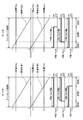
- 11-1 to 11-3 show the R, S, T phase control voltages ka, kb, kc, sawtooth waves 1 and 2 in the first embodiment in the modes I to VI of FIG. It is a figure which shows an example of a R, S, T phase pulse.
- the order of the R, S, and T pulses of the section voltage in modes I to VI is irregular.
- the section 1 voltage is a voltage between STs in mode II, but is a voltage between RTs in mode III. If the pulse order is irregular, charging / discharging of the input capacitor becomes unbalanced, causing a spike-like current waveform as shown in FIG.
- Step-down is performed by turning off the bidirectional switch circuit in at least two phases (R phase, T phase, S phase) and providing a switching section in which no current flows in all phases (intermediate phase) The voltage is dropped without widening the conduction width.
- Step-down is performed by turning off the bidirectional switch circuit in at least two phases (R phase, T phase, S phase) and providing a switching section in which no current flows in all phases (intermediate phase) The voltage is dropped without widening the conduction width.
- (2) Regularly charge and discharge the input capacitor by making the pulse order of the interval voltages in all modes I to VI regular (the same phase in all modes has the same regular switching pattern). .
- the DC voltage can be dropped without increasing the conduction width of the intermediate phase, so that the voltage fluctuation of the input capacitor of the intermediate phase cannot be increased.
- charging / discharging of the input capacitor of each phase can be balanced by making the pulse order of the interval voltage in each mode I to VI regular. As a result, it is possible to prevent spike-like current waveforms during charging / discharging of the input capacitor without increasing the switching frequency.
- the voltage fluctuation of the intermediate phase input capacitor does not increase, it is possible to use an input capacitor having a small capacity.
- the overall configuration of the power conversion apparatus to which the step-down three-phase rectifier according to the second embodiment is applied is the same as that shown in FIG.
- FIG. 12 is a block diagram showing an example of the switching pattern generator 5 of FIG.
- FIG. 13 is a diagram showing a waveform example of sawtooth waves 1 and 2 used when the switching pattern generator 5 generates a switching pattern.
- FIG. 14 is a diagram illustrating a configuration example of the phase voltage discriminator 52 of the switching pattern generator 5.
- FIG. 15 is a circuit diagram showing a configuration example of the pattern signal generator 51 of the switching pattern generator 5.
- the switching pattern generator 5 of the present embodiment generates switching patterns (R, S, T phase pulses) as shown in FIGS. 16 to 18 based on the above guidelines.
- the switching pattern generator 5 detects which phase of the three-phase AC power source 1 is an intermediate potential phase at a predetermined timing such as a rising edge of a switching cycle, and performs switching using a modulation waveform and a sawtooth wave generated according to the detection result.
- a switching pattern is generated by obtaining ON / OFF timing of the pattern.
- the switching pattern generator 5 includes a pattern signal generator 51, a phase voltage discriminator 52, a DC voltage setting unit 53, a sawtooth wave generator 54, and comparators 55-1 to 55-.
- NOT circuits 56-1 and 56-2 OR circuits 57-1 and 57-2, NOT circuits 58-1 and 58-2, AND circuits 59-1 and 59-2, and AND circuit 60R.
- 60T an OR circuit 60S, NAND circuits 61R to 61T, AND circuits 62R to 62T, OR circuits 63R to 63T, and an AND circuit 64.
- the pattern signal generator 51 uses the R-phase voltage normalized signals a and S-phase in which the peak value of the input phase voltage is normalized to “1” in order to regularize the pulse order of the interval voltages in all modes I to VI.
- the voltage standardized signal b and the T-phase voltage standardized signal c are calculated, and a modulation waveform 1, a modulation waveform 2A, a modulation waveform 2B, and a modulation waveform 3 are output.
- the DC voltage setting unit 53 sets a DC voltage setting gain k (where k ⁇ 1) in the sawtooth generator 54.
- the sawtooth wave generator 54 outputs the sawtooth wave 1 and the sawtooth wave 2.
- the phase voltage discriminator 52 compares the potentials of the input R-phase voltage normalized signal a, S-phase voltage normalized signal b, and T-phase voltage normalized signal c, and R-phase middle, S-phase middle, T-phase An intermediate determination signal (“1” for intermediate, “0” for non-intermediate) is output, respectively. Specifically, in the middle of the S phase, modulation waveforms 1 and 3 are output, and sawtooth waves 1 and 2 are output (see FIG. 16).
- the switching pattern generator 5 In the middle of the T phase, the modulation waveforms 1 and 2A are output, and the sawtooth wave 1 is output (see FIG. 17). In the middle of the R phase, the modulation waveforms 3 and 2B are output, and the sawtooth wave 2 is output (see FIG. 18).
- the switching pattern generator 5 the switching pattern generation method is changed according to which phase the intermediate phase is. Thereby, the same regularity is given to the switching pattern of the same phase in all modes.
- the comparison signal obtained by comparing the modulated waveform 1 and the sawtooth wave 1 by the comparator 55-1 and the output obtained by performing NOT operation on the R-phase intermediate signal by the NOT circuit 58-1 are ANDed by the AND circuit 60R, and R Output as a non-intermediate phase pulse.
- the comparison signal obtained by comparing the modulated waveform 2B and the sawtooth wave 2 by the comparator 55-3 and the output obtained by performing NOT operation on the T-phase intermediate signal by the NOT circuit 58-2 are ANDed by the AND circuit 60T. Output as a non-intermediate phase pulse.
- the comparison signal obtained by comparing the modulation waveform 2A and the sawtooth wave 1 by the comparator 55-2A and the output obtained by performing NOT operation on the comparison signal of the comparator 55-1 by the NOT circuit 56-1 are ORed by the OR circuit 57-1. Calculated.
- the comparison signal obtained by comparing the modulation waveform 2B and the sawtooth wave 2 by the comparator 55-2B and the output obtained by performing the NOT operation on the comparison output of the comparator 55-3 by the NOT circuit 56-2 are ORed by the OR circuit 57-2.
- the AND circuit 59-1 performs an AND operation on the OR circuit 57-1 and the T-phase intermediate signal
- the OR circuit 57-2 performs an OR operation on the R-phase intermediate signal. 2 is ANDed by the OR circuit 60S, and an S-phase non-intermediate pulse 27 is output.
- the NAND circuit 61R performs an NAND operation on the S-phase non-intermediate pulse and the T-phase non-intermediate pulse, and the R-phase intermediate signal is AND-operated by the AND circuit 62R to output an R-phase intermediate pulse.
- the NAND circuit 61S performs an NAND operation on the R-phase non-intermediate pulse and the T-phase non-intermediate pulse, and the S-phase intermediate signal is AND-processed by the AND circuit 62S and is output as an S-phase intermediate pulse.
- the NAND circuit 61T performs an NAND operation on the R-phase non-intermediate pulse and the S-phase non-intermediate pulse and the T-phase intermediate signal, and the AND circuit 62T performs an AND operation and outputs the T-phase intermediate pulse.
- the comparator 65 compares the sawtooth wave 1 with the “0” input, and outputs a comparison signal as a 0 voltage insertion signal.
- the OR circuit 63R performs an OR operation on the R-phase non-intermediate pulse and the R-phase intermediate pulse and the 0 voltage insertion signal is AND-processed by the AND circuit 64 and is output as an R-phase pulse. Thereby, a switching pattern (section 4) for turning off the bidirectional switch is introduced into the R-phase pulse.
- the T-phase non-intermediate time pulse and the T-phase intermediate time pulse are ORed and output as a T-phase pulse. Since the output of the OR circuit 63T is “0” during the zero voltage insertion signal period, the T phase pulse is not calculated with the zero voltage insertion signal.
- the S-phase non-intermediate pulse and the S-phase intermediate pulse are ORed to output an S-phase pulse.
- the R-phase pulse and the T-phase pulse are “0” during the zero voltage insertion signal period, and no DC voltage is generated even when the S-phase pulse is ON. For the purpose of not increasing the number of times of T-phase switching, the calculation with the zero voltage insertion signal is not performed.
- the saw-tooth wave generator 54 has a time T based on the DC voltage setting gain k of the DC voltage generator 53, and (time axis kT, gain axis 0) and (time axis 0, A sawtooth wave 1 is output as a straight line connecting the gain axes 1).
- the sawtooth wave generator 54 outputs the sawtooth wave 2 as a straight line connecting (time axis 0, gain axis 0) and (time axis kT, gain axis 1) based on the DC voltage setting gain k.
- the phase voltage discriminator 52 includes comparators 70R, 70S, and 70T, AND circuits 71R, 71S, and 71T, AND circuits 72R, 72S, and 72T, and NOR circuits 73R, 73S, and 73T. ing.
- the comparator 70R compares the R-phase voltage normalized signal a and the S-phase voltage normalized signal b, and compares the comparison signal (“1” when R-phase voltage normalized signal a> S-phase voltage normalized signal b, When the R-phase voltage standardized signal a ⁇ the S-phase voltage standardized signal b, “0”) is output to the AND circuits 71R, 72S, 71T, and 72T.
- the comparator 70S compares the S-phase voltage normalized signal b and the T-phase voltage normalized signal c, and compares the comparison signal (“1” when S-phase voltage normalized signal b> T-phase voltage normalized signal c; When the S-phase voltage normalized signal b ⁇ T-phase voltage normalized signal c, “0”) is output to the AND circuits 71R, 72R, 71S, and 72T.
- the comparator 70T compares the T-phase voltage normalized signal c and the R-phase voltage normalized signal a, and compares the comparison signal (“1” when T-phase voltage normalized signal c> R-phase voltage normalized signal a; When the T-phase voltage normalized signal c ⁇ the R-phase voltage normalized signal a, “0”) is output to the AND circuits 72R, 71S, 72S, 71T.
- the AND circuit 71R outputs an AND operation result of the comparison signal of the comparator 70R and the comparison signal of the comparator 70S.
- the AND circuit 72R outputs an AND operation result of the comparison signal of the comparator 70S and the comparison signal of the comparator 70T.
- the AND circuit 71S outputs an AND operation result of the comparison signal of the comparator 70S and the comparison signal of the comparator 70T.
- the AND circuit 72S outputs an AND operation result of the comparison signal of the comparator 70T and the comparison signal of the comparator 70R.
- the AND circuit 71T outputs an AND operation result of the comparison signal of the comparator 70T and the comparison signal of the comparator 70R.
- the AND circuit 72T outputs an AND operation result of the comparison signal of the comparator 70R and the comparison signal of the comparator 70S.
- the NOR circuit 73R outputs a NOR operation result (“1” when intermediate, “0” when not intermediate) between the output of the AND circuit 71R and the output of the AND circuit 72R as an R-phase intermediate signal.
- the NOR circuit 73S outputs a NOR operation result (“1” when intermediate, “0” when not intermediate) between the output of the AND circuit 71S and the output of the AND circuit 72S as an S-phase intermediate signal.
- the NOR circuit 73T outputs a NOR operation result (“1” when intermediate, “0” when not intermediate) between the output of the AND circuit 71T and the output of the AND circuit 72T as a T-phase intermediate signal.
- the pattern signal generator 51 that forms each modulation waveform includes absolute value circuits 80R, 80S, and 80T, and 3-input adders 81-1 and 81-2.
- the absolute value circuit 80R calculates the absolute value
- the absolute value circuit 80S calculates and outputs the absolute value
- the absolute value circuit 80T calculates the absolute value
- the 3-input adder 81-1 adds the modulation waveform 1, the output of the absolute value circuit 80S, and the constant ⁇ 1, and outputs a modulation waveform 2A.
- the 3-input adder 81-2 adds the modulation wavelength 3, the output of the absolute value circuit 80S, and the constant ⁇ 1, and outputs a modulation waveform 2B.
- FIG. 16 is a diagram illustrating an example of a modulation waveform, a sawtooth wave, and R, S, and T phase pulses in modes II and V.
- FIG. 17 is a diagram illustrating an example of a modulation waveform, a sawtooth wave, and R, S, and T phase pulses in modes I and IV.
- FIG. 18 is a diagram illustrating an example of a modulation waveform, a sawtooth wave, and R, S, and T phase pulses in modes III and VI.
- the R-phase pulse is OFF ⁇ ON ⁇ OFF
- the S-phase pulse is ON ⁇ OFF ⁇ ON
- the T-phase pulse is ON ⁇ OFF.
- the same phase in all modes I to VI has the same regularity pattern in which the ON and OFF changes are regular.
- the R-phase pulse has a period (section 4) in which the zero voltage insertion signal is inserted.
- the period in which the zero voltage insertion signal is inserted is A switching pattern for turning off the direction switch circuit is inserted. Accordingly, in section 4, two of the three phases (R phase and T phase) are turned off, so that no current flows in all phases.
- the timing (section 1) when the R-phase pulse is turned on is obtained from the intersection of the R-phase voltage
- the timing (section 1 + section 2) when the T-phase pulse is turned off is obtained from the intersection of the T-phase voltage
- the intermediate phase pulse is turned ON when either the maximum phase pulse or the minimum phase pulse is OFF.
- the S-phase pulse is obtained from the intersection between the R-phase voltage
- the widths of the sections 1, 2, 3, 4 are kT ⁇ (1 ⁇
- the average of the DC voltage in the switching period T can be expressed as follows by integrating the DC voltage for each section, adding each, and dividing by the switching period T.
- the input current As the R-phase input current, a positive current proportional to the time of the R-phase voltage a flows. As the T-phase input current, a negative current proportional to the magnitude of the T-phase voltage
- flows. As for the S-phase input current, a positive current flows in section 1 and a negative current flows in section 3. Therefore, the flowing current is kT ⁇ (1 ⁇ a) ⁇ kT ⁇ (1 + c) ⁇ kT ( ⁇ ac) kTb, and the interval 4 in which the 0 voltage insertion signal is inserted in the switching period T is excluded. When divided by the period kT, the S-phase voltage b is obtained. Therefore, a current proportional to the R-phase voltage a, the S-phase voltage b, and the T-phase voltage c flows through the R phase, S phase, and T phase, resulting in a sine wave current.
- the widths of the sections 1, 2, 3, and 4 are kT ⁇ (1 ⁇
- the average of the DC voltage in the switching period T can be expressed as follows.
- a positive current proportional to the time of the R-phase voltage a flows in the maximum R-phase.
- a negative current proportional to the time of the S phase voltage b flows in the S phase of the minimum phase.
- a negative current flows in section 1 and a positive current flows in section 2.
- each phase pulse will be described.
- the S phase is the maximum phase
- the T phase is the minimum phase
- the R phase is the intermediate phase.
- the modulation waveform 3, 2B and the sawtooth wave 2 are used to obtain the ON / OFF timing of each phase pulse shown in FIG.
- the widths of the sections 1, 2, 3, and 4 are kT ⁇ (
- the average of the DC voltage in the switching period T can be expressed as follows.
- the DC voltage can be controlled to a voltage proportional to k in all modes, and the input current can be a sine wave.
- the voltage is stepped down by introducing the section where the current does not flow in all phases of the switching pattern within each switching cycle.
- the DC voltage can be lowered without increasing the width, and the voltage fluctuation of the intermediate phase input capacitor can be reduced.
- an input capacitor having a very small capacity can be used.
- the mode is divided into a plurality of modes according to the magnitude relation of the voltage of each phase, and a different switching pattern is generated for each phase in each mode.
- the switching pattern is the same phase in all modes. Since the patterns have the same regularity, charging / discharging of the input capacitors of each phase can be balanced. Thereby, a spike-like current waveform at the time of charging / discharging of the input capacitor can be prevented without increasing the switching frequency.
- the present invention is not limited to the second embodiment, and as the bidirectional switch circuit 3, the circuit shown in FIG. 22 can be made to function in the same manner by connecting it to FIGS. is there.
- the circuit of FIG. 22 is obtained by connecting a free-wheeling current diode D1 when 0 voltage is inserted to the output side of the circuit of FIG.
- a carrier waveform such as a triangular wave may be used. .
- the three-phase rectifier according to the present invention can be widely used in various devices, and in particular, air conditioners, refrigerators, washing machines, cleaners, ventilation fans, and motor drive devices and motor drive inverter controls used for these. Useful for devices and the like.
Landscapes
- Engineering & Computer Science (AREA)
- Power Engineering (AREA)
- Rectifiers (AREA)
- Inverter Devices (AREA)
Abstract
Description
2 直流リアクトル
3 双方向スイッチ回路
4 全波整流回路
5 スイッチングパターン発生器
6 駆動回路
7 負荷
8 3相リアクトル
9 入力コンデンサ
11 パターン信号発生器
12 電圧設定器
13 相電圧判別器
14R~14T、15R~15T コンパレータ
16R~16T、17R~17T、18R~18T AND回路
19R~19T OR回路
51 パターン信号発生器
52 相電圧判別器
53 直流電圧設定器
54 鋸歯状波発生器
55-1~55-3 コンパレータ
56-1,56-2 NOT回路
57-1,57-2 OR回路 57-1,57-2と、OR回路57-1,57-2
58-1,58-2 NOT回路
59-1,59-2 AND回路
60R~60T AND回路
60S~60T OR回路
61~61T NAND回路
62R~62T AND回路
63R~63T R回路
61 AND回路
[3相整流器の構成例]
図1は、実施の形態1にかかる降圧型の3相整流器を適用した電力変換装置の一構成例を示す図である。本実施の形態の電力変換装置は、図1に示すように、R,S,T相電圧を発生させる3相交流電源1と、3相交流電源1の出力側に接続された3相リアクトル8および入力コンデンサ9と、3相電圧を直流電圧に整流する、6つのダイオードを備えた全波整流回路4と、全波整流回路4の各相の入力をON/OFFする双方向スイッチ回路3と、3相の相電圧を検出して、双方向スイッチ回路3のスイッチングパターンを生成するスイッチングパターン発生器5と、スイッチングパターン発生器5で生成されたスイッチングパターンに基づいて、双方向スイッチ回路3のスイッチング素子をスイッチング制御する駆動回路6と、全波整流回路4の出力側に接続された直流リアクトル2およびコンデンサ10と、コンデンサ10に並列に接続され、直流電力が供給される負荷7とを備えている。
図3は、スイッチングパターン発生器5の一例を示すブロック図である。図4は、スイッチングパターン発生器5でスイッチングパターンを生成する場合に使用される鋸歯状波1、2の波形例を示す図である。図5は、スイッチングパターン発生器5のパターン信号発生器11の構成例を示す回路図である。図6は、スイッチングパターン発生器5の相電圧判別器13の構成例を示す図である。
つぎに、本実施の形態での直流電圧の脈動と入力電流の高調波を低減する原理を説明する。本実施の形態では、スイッチングパターン発生器5および駆動回路6によって、双方向スイッチ回路3を以下のようにスイッチングすることで、直流電圧の脈動と入力電流の高調波を低減している。図7は、R相電圧、S相電圧、T相電圧の各区間を説明するための図である。図8は、R,S,T相制御電圧ka、kb、kcと、鋸歯状波1、2と、R,S,T相パルス(スイッチングパターン)の一例を示す図である。
スイッチング周期Tの電圧の平均={(b-c)×T×(1-ka)+(a-c)×T×(ka-kc-1)+(a-b)×T×(1+kc)}/T
=k(a2+c2)-kb(a+c)
ここで、a+b+c=0(3相条件)を考慮すると、
=k(a2+b2+c2)
さらに、交流理論から、a2+b2+c2=3/2より
=k×3/2
なお、上記スイッチング周期Tの電圧の平均は、相電圧に基づいて表されている。
(1)スイッチング周期Tにおける直流電圧の平均値は、降圧された一定の電圧値となる。
(2)スイッチング周期Tにおける入力電流の平均値は、入力の電圧比に分配される。
P=Vsin(ωt)×I(t)sin(ωt)+Vsin(ωt+120)×I(t)sin(ωt+120)Vsin(ωt+240)+I(t)sin(ωt+240) =V×I(t)sin2(ωt)+V×I(t)sin2(ωt+120)+V×I(t)sin2(ωt+240)
=V×I(t){sin2(ωt)+sin2(ωt+120)+sin2(ωt+240)}
{ }内を計算すると、{ }内は、定数3/2であるので、
P=V×I(t)×3/2を変形して、I(t)=P/V×2/3
ここで、Pが一定の場合、Vは一定であるので、I(t)は、時間に依存しない一定値となる。即ち、入力電流は、正弦波である。
(3)上記(2)の条件の下で、電力が一定である場合、入力電流は正弦波となる。
図9を参照して、本実施の形態による直流電圧および直流電流のシミュレーション結果について説明する。図9は、上記図1の回路の直流電圧および直流電流のシミュレーション結果を示している。図1の回路において、直流入力電圧3相=200V(線間電圧)、負荷7として負荷抵抗=20Ω、入力の3相リアクトル8として系統のリアクタンスを考慮して100μH、入力コンデンサ9=3μF/相、コンデンサ10=2μF、直流リアクトル2=2mH、スイッチング周波数50kHz、直流電圧設定ゲインk=0.9の条件でシミュレーションを行った。3相電圧の全波整流のリップルの下限の電圧(直流電圧として取り出せる最大の電圧)は200×21/2×(31/2/2)=245Vであるのに対し、図9に示すように、本実施の形態では、直流電圧は、約DC220Vで一定で理論通りであり、降圧されており、また、直流電流も一定となっており、入力電流もスイッチングに伴う変動はあるものの正弦波状になっている。なお、上記シミュレーションは、線間電圧に基づいており、直流電圧と直流電流はそれぞれ負荷10の両端の電圧と負荷10に流入する電流である。
リップルの平滑には無関係である。
図11-1~図22を参照して、実施の形態2に係る三相整流器について説明する。上記実施の形態1の3相整流器によれば、容量の小さいコンデンサやリアクトルを使用した場合でも、直流電圧の脈動や入力電流の高調波を低減することが可能となる。本願出願人は、より容量の小さいコンデンサやリアクトルを使用した場合でも、直流電圧の脈動や入力電流の高調波を低減するために、上記実施の形態1の改善点を検討した。
(1)全相(R相、T相、S相)の少なくとも2つの相で双方向スイッチ回路をOFFにして、全相で電流が流れないスイッチング区間を設けることによって、降圧を行う(中間相の導通幅を広げずに電圧を降下する)。
(2)全モードI~VIでの区間電圧のパルス順序を規則的(全モードで同一の相は、同一の規則性のあるスイッチングパターン)とすることによって、入力コンデンサを規則的に充放電させる。
図12は、図1のスイッチングパターン発生器5の一例を示すブロック図である。図13は、スイッチングパターン発生器5でスイッチングパターンを生成する場合に使用される鋸歯状波1、2の波形例を示す図である。図14は、スイッチングパターン発生器5の相電圧判別器52の構成例を示す図である。図15は、スイッチングパターン発生器5のパターン信号発生器51の構成例を示す回路図である。
図16~図18を参照して、上記図7の各モードI~VIでのスイッチング動作による直流電圧・各相の電流を説明する。モードIとモードIVでは共にT相が中間相となり、モードIIとモードVでは共にS相が中間相となり、モードIIIとモードVIでは共にR相が中間相となるので、以下、モードI、II、IIIについて説明する。図16は、モードII、Vにおける、変調波形と、鋸歯状波と、R,S,T相パルスの一例を示す図である。図17は、モードI、IVにおける、変調波形と、鋸歯状波と、R,S,T相パルスの一例を示す図である。図18は、モードIII、VIにおける、変調波形と、鋸歯状波と、R,S,T相パルスの一例を示す図である。
まず、直流電圧について説明する。図16において、区間1、2、3、4の直流電圧は、それぞれST間電圧=b-c、RT間電圧=a-c、RS間電圧=a-b、整流器出力短絡電圧=0となる。次に、各相パルスについて説明する。モードIIでは、R相が最大相、T相が最小相、S相が中間相となる。実施の形態1(図8)と同様に、最大相と最小相では、パルスはそれぞれの電位に比例する時間ONとなる。したがって、R相のパルス幅x=kT|a|、T相のパルス幅z=kT|c|となる。ここで、R相パルスがONとなるタイミング(区間1)は、R相電圧|a|と鋸歯状波1との交点から求められる。また、R相パルスがOFFとなるタイミング(区間1+区間2+区間3)は、鋸歯状波1とゲイン軸0との交点から求められる。これにより、R相パルスが得られる。一方、T相パルスがOFFとなるタイミング(区間1+区間2)は、T相電圧|c|と鋸歯状波2との交点から求められる。これにより、T相パルスが得られる。中間相パルスは、最大相又は最小相のパルスのどちらかがOFFのときにONする。したがって、S相パルスは、R相電圧|a|と鋸歯状波1との交点、およびT相電圧|c|と鋸歯状波2との交点から求められる。また、区間1、2、3、4の幅は、それぞれkT×(1-|a|)、kT×(|a|+|c|-1)、kT×(1-|c|)、T×(1-k)となる。スイッチング周期Tの直流電圧の平均は、それぞれの区間ごとに直流電圧を積算しそれぞれを加算してスイッチング周期Tで除して、以下のように表すことができる。スイッチング周期Tの直流電圧の平均={(b-c)×kT×(1-a)+(a-c)×kT×(a-c-1)+(a-b)×kT×(1+c)+0×T×(1-k)}/T
=k{a2+c2-b(a+c)}
ここで、a+b+c=0(3相条件)を考慮すると、
=k(a2+b2+c2)
さらに、交流理論から、a2+b2+c2=3/2より、
=k×3/2
このように、kに比例する一定電圧となる。
図17において、区間1、2、3、4の直流電圧は、それぞれST間電圧=c-b、RT間電圧=a-c、RS間電圧=a-b、整流器出力短絡電圧=0となる。次に各相のパルスについて説明する。モードIでは、R相が最大相、S相が最小相、T相が中間相となる。R,S,T相のパルスのON、OFF順序を変えずに、最大相と最小相でそれぞれの電位に比例する時間ONとするため、モードIでは、変調波形1,2Aと鋸波状波1を用いて、図17に示す各パルスのON,OFFタイミングを得る。また、区間1、2、3、4の幅は、それぞれkT×(1-|a|)、kT(1-|b|)、kT×(|a|-|b|-1)、T×(1-k)となる。スイッチング周期Tの直流電圧の平均は、以下のように表すことができる。
=k{a2+b2-c(a+b)}
ここで、a+b+c=0(3相条件)を考慮すると、
=k(a2+b2+c2)
さらに、交流理論から、a2+b2+c2=3/2より
、
=k×3/2
このように、kに比例する一定電圧となる。
図18において、区間1、2、3、4の直流電圧は、それぞれST間電圧=b-c、RT間電圧=a-c、RS間電圧=b-a、整流器出力短絡電圧=0となる。次に、各相のパルスについて説明する。モードIIIでは、S相が最大相、T相が最小相、R相が中間相となる。モードIと同じく、R,S,T相のパルスのON,OFF順序を変えずに、最大相と最小相でそれぞれの電位に比例する時間をONとするため、モードIIIでは、変調波形3、2Bと鋸歯状波2を用いて、図18に示す各相パルスのON,OFFタイミングを得る。また、区間1、2、3、4の幅は、それぞれ、kT×(|b|+|c|-1)、kT×(1-|b|)、kT×(1-|c|)、T×(1-k)となる。スイッチング周期Tの直流電圧の平均は、以下のように表すことができる。
=k{b2+c2-a(b+c)}
ここで、a+b+c=0(3相条件)を考慮すると、
=k(a2+b2+c2)
さらに、交流理論から、a2+b2+c2=3/2より
、
=k×3/2
このように、kに比例する一定電圧となる。
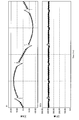
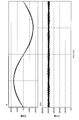
図19~図21を参照して、本実施の形態による直流電圧および直流電流(R相電流)のシミュレーション結果について説明する。入力コンデンサの容量およびスイッチング周波数以外は、上記実施の形態1のシミュレーションの条件と同じ条件でシミュレーションを行った。
Claims (7)
- 3相交流電源から供給される3相交流電力を直流電力に変換する3相整流器において、
前記3相交流電力を直流電力に整流する全波整流回路と、
前記3相交流電源から前記全波整流回路への各相の入力をON/OFFする双方向スイッチ回路と、
前記3相交流電源の各相の電圧を検出して、各相の検出電圧に基づいて、前記双方向スイッチ回路をON/OFFさせるための各相のスイッチングパターンを生成し、生成したスイッチングパターンに基づいて、前記双方向スイッチ回路をスイッチング制御する制御手段と、
を備えたことを特徴とする3相整流器。 - 前記各相のスイッチングパターンは、所定のスイッチング周期を有しており、
前記制御手段は、前記3相電源の各相の電圧の最大電位相、中間電位相、および最小電位相を検出し、最大電位相および最小電位相の場合は、それぞれの電位に比例する時間ONとなり、かつ、前記スイッチング周期内で少なくとも一方はONとなるスイッチングパターンを生成し、また、中間電位相の場合は、常にONとなるスイッチングパターンを生成することを特徴とする請求項1に記載の3相整流器。 - 前記3相交流電源と前記双方向スイッチ回路との間にコンデンサを接続したことを特徴とする請求項1に記載の3相整流器。
- 前記全波整流回路と負荷との間に、直流リアクトルを接続したことを特徴とする請求項1に記載の3相整流器。
- 前記制御手段は、各相の電圧の大小関係により、複数のモードに区分し、各モードで各相毎に、異なるスイッチングパターンを生成し、
前記スイッチングパターンは、全モードで同一の相は、同一の規則性のあるパターンであることを特徴とする請求項1に記載の3相整流器。 - 前記各相のスイッチングパターンは、所定のスイッチング周期を有しており、
前記制御手段は、各スイッチング周期内で、少なくとも2つの相がOFFする期間を導入したことを特徴とする請求項5に記載の3相整流器。 - 前記制御手段は、1相のスイッチングパターンに0電圧を挿入することを特徴とする請求項6に記載の3相整流器。
Priority Applications (4)
| Application Number | Priority Date | Filing Date | Title |
|---|---|---|---|
| US13/380,363 US8817505B2 (en) | 2009-06-26 | 2010-06-28 | Three-phase rectifier with bidirectional switches |
| EP10792226.2A EP2448101B1 (en) | 2009-06-26 | 2010-06-28 | Three-phase rectifier |
| AU2010263537A AU2010263537B2 (en) | 2009-06-26 | 2010-06-28 | Three-phase rectifier |
| CN201080028301.5A CN102598497B (zh) | 2009-06-26 | 2010-06-28 | 三相整流器 |
Applications Claiming Priority (4)
| Application Number | Priority Date | Filing Date | Title |
|---|---|---|---|
| JP2009-152770 | 2009-06-26 | ||
| JP2009152770 | 2009-06-26 | ||
| JP2010110435A JP4687824B2 (ja) | 2009-06-26 | 2010-05-12 | 3相整流器 |
| JP2010-110435 | 2010-05-12 |
Publications (1)
| Publication Number | Publication Date |
|---|---|
| WO2010150909A1 true WO2010150909A1 (ja) | 2010-12-29 |
Family
ID=43386676
Family Applications (1)
| Application Number | Title | Priority Date | Filing Date |
|---|---|---|---|
| PCT/JP2010/060976 Ceased WO2010150909A1 (ja) | 2009-06-26 | 2010-06-28 | 3相整流器 |
Country Status (6)
| Country | Link |
|---|---|
| US (1) | US8817505B2 (ja) |
| EP (1) | EP2448101B1 (ja) |
| JP (1) | JP4687824B2 (ja) |
| CN (1) | CN102598497B (ja) |
| AU (1) | AU2010263537B2 (ja) |
| WO (1) | WO2010150909A1 (ja) |
Cited By (2)
| Publication number | Priority date | Publication date | Assignee | Title |
|---|---|---|---|---|
| JP2015195654A (ja) * | 2014-03-31 | 2015-11-05 | 株式会社富士通ゼネラル | 整流器 |
| US20150372610A1 (en) * | 2013-01-23 | 2015-12-24 | Fujitsu General Limited | Matrix converter |
Families Citing this family (16)
| Publication number | Priority date | Publication date | Assignee | Title |
|---|---|---|---|---|
| FR2973181B1 (fr) * | 2011-03-21 | 2014-05-16 | Hispano Suiza Sa | Procede de commande simplifie d'un convertisseur de tension alternative triphasee en tension continue |
| JP5938988B2 (ja) * | 2012-03-29 | 2016-06-22 | 株式会社富士通ゼネラル | パワーモジュール |
| JP5994334B2 (ja) * | 2012-03-29 | 2016-09-21 | 株式会社富士通ゼネラル | 3相スイッチ整流器 |
| DE102012218512A1 (de) * | 2012-10-11 | 2014-04-17 | Robert Bosch Gmbh | Vorrichtung und Verfahren zum Laden eines elektrischen Energiespeichers aus einer dreiphasigen Wechselspannungsquelle |
| JP6146054B2 (ja) * | 2013-02-28 | 2017-06-14 | 株式会社富士通ゼネラル | 3相整流器 |
| JP6201371B2 (ja) * | 2013-03-28 | 2017-09-27 | 株式会社富士通ゼネラル | 3相整流器 |
| US20150102671A1 (en) * | 2013-10-15 | 2015-04-16 | General Electric Company | Direct current power transmission system |
| JP2016046957A (ja) * | 2014-08-25 | 2016-04-04 | 株式会社安川電機 | マトリクスコンバータ、マトリクスコンバータの制御装置およびマトリクスコンバータの制御方法 |
| US10177572B2 (en) | 2015-03-31 | 2019-01-08 | Fujitsu General Limited | DC/AC system interconnection device and AC/AC system interconnection device |
| US10027244B2 (en) * | 2016-06-21 | 2018-07-17 | General Electric Company | Active voltage regulator systems and methods |
| AT524638A1 (de) * | 2017-01-05 | 2022-07-15 | Int Power Electronics Consulting Ipec Gmbh | Dreiphasen-Hoch-Tiefsetz-Gleichrichtersystem mit sinusförmigem Eingangsstrom und geregelter gleichtaktfreier Ausgangsspannung |
| JP7259450B2 (ja) * | 2019-03-20 | 2023-04-18 | 株式会社富士通ゼネラル | 三相整流器及び三相整流器の制御方法 |
| CN111674275A (zh) * | 2020-06-18 | 2020-09-18 | 薛洛良 | 采用变压器输出1250伏电压的电动车直流充电系统 |
| EP4138289A1 (en) | 2021-08-19 | 2023-02-22 | Carrier Corporation | Dual mode converter for air conditioning system |
| JPWO2024013889A1 (ja) * | 2022-07-13 | 2024-01-18 | ||
| CN115864873B (zh) * | 2022-12-01 | 2025-07-11 | 东南大学 | 一种电压控制型逆变器的幅相模型建立及控制方法 |
Citations (6)
| Publication number | Priority date | Publication date | Assignee | Title |
|---|---|---|---|---|
| JPS59139868A (ja) | 1983-01-28 | 1984-08-10 | Hitachi Ltd | パルス幅変調式コンバ−タの制御装置 |
| JPH0265667A (ja) * | 1988-08-27 | 1990-03-06 | Hitachi Ltd | コンバータの制御装置 |
| GB2294165A (en) | 1994-10-11 | 1996-04-17 | Lumonics Ltd | Power supply for providing a dc supply from a multiphase ac source |
| JPH09275685A (ja) * | 1996-02-06 | 1997-10-21 | Mitsubishi Electric Corp | 電源高調波抑制装置 |
| JP2004343975A (ja) * | 2003-05-19 | 2004-12-02 | Sanken Electric Co Ltd | 三相スイッチング整流装置 |
| JP2005143212A (ja) | 2003-11-06 | 2005-06-02 | Fuji Electric Holdings Co Ltd | 三相降圧形整流器 |
Family Cites Families (8)
| Publication number | Priority date | Publication date | Assignee | Title |
|---|---|---|---|---|
| AT406434B (de) * | 1993-12-23 | 2000-05-25 | Ixys Semiconductor Gmbh | Vorrichtung zur umformung eines dreiphasigen spannungssystems in eine vorgebbare, einen verbraucher speisende gleichspannung |
| JP2865194B2 (ja) * | 1994-07-29 | 1999-03-08 | 株式会社アイ・ヒッツ研究所 | 単相入力3相全波整流回路及び単相入力疑似4相全波整流回路 |
| CN1134101C (zh) * | 2000-07-28 | 2004-01-07 | 上海新源变频电器有限公司 | 整流电源装置 |
| JP4858937B2 (ja) * | 2004-11-12 | 2012-01-18 | 富士電機株式会社 | 発電電力の系統連系装置 |
| KR100949639B1 (ko) * | 2005-04-27 | 2010-03-26 | 가부시키가이샤 야스카와덴키 | 전력 변환 장치와 전력 변환 방법 |
| JP4808221B2 (ja) * | 2005-12-12 | 2011-11-02 | 株式会社千代田 | 高周波変復調多相整流装置 |
| US8223517B2 (en) * | 2006-04-25 | 2012-07-17 | Mitsubishi Electric Corporation | Power converting apparatus with main converter and sub-converter |
| US8576593B2 (en) * | 2009-01-13 | 2013-11-05 | Mitsubishi Electric Corporation | AC-DC power converting apparatus having sub-converters connected in series between main converter and AC power supply |
-
2010
- 2010-05-12 JP JP2010110435A patent/JP4687824B2/ja active Active
- 2010-06-28 EP EP10792226.2A patent/EP2448101B1/en active Active
- 2010-06-28 AU AU2010263537A patent/AU2010263537B2/en active Active
- 2010-06-28 WO PCT/JP2010/060976 patent/WO2010150909A1/ja not_active Ceased
- 2010-06-28 CN CN201080028301.5A patent/CN102598497B/zh active Active
- 2010-06-28 US US13/380,363 patent/US8817505B2/en active Active
Patent Citations (6)
| Publication number | Priority date | Publication date | Assignee | Title |
|---|---|---|---|---|
| JPS59139868A (ja) | 1983-01-28 | 1984-08-10 | Hitachi Ltd | パルス幅変調式コンバ−タの制御装置 |
| JPH0265667A (ja) * | 1988-08-27 | 1990-03-06 | Hitachi Ltd | コンバータの制御装置 |
| GB2294165A (en) | 1994-10-11 | 1996-04-17 | Lumonics Ltd | Power supply for providing a dc supply from a multiphase ac source |
| JPH09275685A (ja) * | 1996-02-06 | 1997-10-21 | Mitsubishi Electric Corp | 電源高調波抑制装置 |
| JP2004343975A (ja) * | 2003-05-19 | 2004-12-02 | Sanken Electric Co Ltd | 三相スイッチング整流装置 |
| JP2005143212A (ja) | 2003-11-06 | 2005-06-02 | Fuji Electric Holdings Co Ltd | 三相降圧形整流器 |
Non-Patent Citations (5)
Cited By (3)
| Publication number | Priority date | Publication date | Assignee | Title |
|---|---|---|---|---|
| US20150372610A1 (en) * | 2013-01-23 | 2015-12-24 | Fujitsu General Limited | Matrix converter |
| US9979311B2 (en) * | 2013-01-23 | 2018-05-22 | Fujitsu General Limited | Matrix converter |
| JP2015195654A (ja) * | 2014-03-31 | 2015-11-05 | 株式会社富士通ゼネラル | 整流器 |
Also Published As
| Publication number | Publication date |
|---|---|
| US8817505B2 (en) | 2014-08-26 |
| EP2448101A4 (en) | 2017-09-13 |
| EP2448101A1 (en) | 2012-05-02 |
| JP2011030409A (ja) | 2011-02-10 |
| AU2010263537A1 (en) | 2012-01-19 |
| JP4687824B2 (ja) | 2011-05-25 |
| CN102598497A (zh) | 2012-07-18 |
| AU2010263537B2 (en) | 2014-06-26 |
| US20120106213A1 (en) | 2012-05-03 |
| CN102598497B (zh) | 2015-08-19 |
| EP2448101B1 (en) | 2021-05-26 |
Similar Documents
| Publication | Publication Date | Title |
|---|---|---|
| JP4687824B2 (ja) | 3相整流器 | |
| JP3422218B2 (ja) | コンバータ | |
| US7613018B2 (en) | Apparatus and method for supplying DC power source | |
| US7532491B2 (en) | Apparatus and method for supplying DC power source | |
| US20140098584A1 (en) | Passive power factor correction incorporating ac/dc conversion | |
| JP4340843B2 (ja) | 交流直流複合電源装置 | |
| Lin et al. | Single-phase power-factor-correction AC/DC converters with three PWM control schemes | |
| JPH09275685A (ja) | 電源高調波抑制装置 | |
| Tang et al. | An improved burst-mode control for VIENNA rectifiers to mitigate DC voltage ripples at light load | |
| JP6361539B2 (ja) | 変換装置 | |
| JP2001016798A (ja) | 電池または電気二重層キャパシタの充放電装置 | |
| Burlaka et al. | Development of single-phase high-power factor inverter welding sources | |
| KR101228451B1 (ko) | 공조기의 직류전원 공급 장치 및 방법 | |
| JPH1198847A (ja) | 整流回路 | |
| JP2016111764A (ja) | 不平衡補正装置、不平衡補正方法及びプログラム | |
| JP2858520B2 (ja) | 力率改善平滑回路 | |
| JPH09252578A (ja) | 高調波電流低減回路 | |
| CN111585433B (zh) | 一种通用接口、控制方法及储能系统 | |
| JP2024143604A (ja) | ブリッジレス力率改善コンバータ及び制御方法 | |
| JPH0765987A (ja) | インバータ式x線高電圧装置 | |
| Maheshwari et al. | Performance Evaluation of Small DC-Link Capacitor Based Drive Under Grid Disturbance Conditions | |
| JP2017085768A (ja) | Dc−acインバータ装置 | |
| JP2024143603A (ja) | ブリッジレス力率改善コンバータ及び制御方法 | |
| JPH0487592A (ja) | 巻線形誘導電動機の速度制御装置 | |
| JP5994334B2 (ja) | 3相スイッチ整流器 |
Legal Events
| Date | Code | Title | Description |
|---|---|---|---|
| WWE | Wipo information: entry into national phase |
Ref document number: 201080028301.5 Country of ref document: CN |
|
| 121 | Ep: the epo has been informed by wipo that ep was designated in this application |
Ref document number: 10792226 Country of ref document: EP Kind code of ref document: A1 |
|
| WWE | Wipo information: entry into national phase |
Ref document number: 2010263537 Country of ref document: AU |
|
| WWE | Wipo information: entry into national phase |
Ref document number: 13380363 Country of ref document: US Ref document number: 2010792226 Country of ref document: EP |
|
| NENP | Non-entry into the national phase |
Ref country code: DE |
|
| ENP | Entry into the national phase |
Ref document number: 2010263537 Country of ref document: AU Date of ref document: 20100628 Kind code of ref document: A |