WO2011102017A1 - アンテナ及び無線通信装置 - Google Patents
アンテナ及び無線通信装置 Download PDFInfo
- Publication number
- WO2011102017A1 WO2011102017A1 PCT/JP2010/068887 JP2010068887W WO2011102017A1 WO 2011102017 A1 WO2011102017 A1 WO 2011102017A1 JP 2010068887 W JP2010068887 W JP 2010068887W WO 2011102017 A1 WO2011102017 A1 WO 2011102017A1
- Authority
- WO
- WIPO (PCT)
- Prior art keywords
- electrode
- antenna
- radiation electrode
- dielectric substrate
- branch
- Prior art date
- Legal status (The legal status is an assumption and is not a legal conclusion. Google has not performed a legal analysis and makes no representation as to the accuracy of the status listed.)
- Ceased
Links
Images


Classifications
-
- H—ELECTRICITY
- H01—ELECTRIC ELEMENTS
- H01Q—ANTENNAS, i.e. RADIO AERIALS
- H01Q1/00—Details of, or arrangements associated with, antennas
- H01Q1/36—Structural form of radiating elements, e.g. cone, spiral, umbrella; Particular materials used therewith
- H01Q1/38—Structural form of radiating elements, e.g. cone, spiral, umbrella; Particular materials used therewith formed by a conductive layer on an insulating support
-
- H—ELECTRICITY
- H01—ELECTRIC ELEMENTS
- H01Q—ANTENNAS, i.e. RADIO AERIALS
- H01Q1/00—Details of, or arrangements associated with, antennas
- H01Q1/12—Supports; Mounting means
- H01Q1/22—Supports; Mounting means by structural association with other equipment or articles
- H01Q1/2283—Supports; Mounting means by structural association with other equipment or articles mounted in or on the surface of a semiconductor substrate as a chip-type antenna or integrated with other components into an IC package
-
- H—ELECTRICITY
- H01—ELECTRIC ELEMENTS
- H01Q—ANTENNAS, i.e. RADIO AERIALS
- H01Q5/00—Arrangements for simultaneous operation of antennas on two or more different wavebands, e.g. dual-band or multi-band arrangements
- H01Q5/30—Arrangements for providing operation on different wavebands
- H01Q5/307—Individual or coupled radiating elements, each element being fed in an unspecified way
- H01Q5/342—Individual or coupled radiating elements, each element being fed in an unspecified way for different propagation modes
- H01Q5/357—Individual or coupled radiating elements, each element being fed in an unspecified way for different propagation modes using a single feed point
- H01Q5/364—Creating multiple current paths
- H01Q5/371—Branching current paths
-
- H—ELECTRICITY
- H01—ELECTRIC ELEMENTS
- H01Q—ANTENNAS, i.e. RADIO AERIALS
- H01Q5/00—Arrangements for simultaneous operation of antennas on two or more different wavebands, e.g. dual-band or multi-band arrangements
- H01Q5/30—Arrangements for providing operation on different wavebands
- H01Q5/378—Combination of fed elements with parasitic elements
-
- H—ELECTRICITY
- H01—ELECTRIC ELEMENTS
- H01Q—ANTENNAS, i.e. RADIO AERIALS
- H01Q9/00—Electrically-short antennas having dimensions not more than twice the operating wavelength and consisting of conductive active radiating elements
- H01Q9/04—Resonant antennas
- H01Q9/30—Resonant antennas with feed to end of elongated active element, e.g. unipole
- H01Q9/42—Resonant antennas with feed to end of elongated active element, e.g. unipole with folded element, the folded parts being spaced apart a small fraction of the operating wavelength
Definitions
- the present invention relates to an antenna used in a plurality of frequency bands, and more particularly to a surface-mount antenna having a radiation electrode formed on a dielectric substrate and a wireless communication apparatus including the same.
- Patent Document 1 discloses an antenna in which a radiation electrode is formed on the surface of a dielectric substrate so as to be used in a plurality of frequency bands.
- FIG. 1 is a perspective view of an antenna disclosed in Patent Document 1.
- the surface-mounted antenna 1 includes a rectangular parallelepiped dielectric base 2, a loop-shaped radiation electrode 3 and a feeding electrode 4 formed on the dielectric base 2.
- the power supply electrode 4 is formed from the bottom surface 2c to the side surface 2b of the dielectric substrate 2, and is formed toward the upper surface 2a through the lateral edge region of the side surface 2b.
- the radiation electrode 3 is formed in a loop shape along each side in the vicinity of each side of the rectangular upper surface 2 a from the power supply electrode 4.
- the open end 3a of the loop-shaped radiation electrode 3 is disposed opposite to the protruding electrode portion 18 on the power supply end side with a predetermined interval, and a capacitance is generated between the open end 3a and the extended electrode on the power supply end portion side. It is configured as follows.
- a capacitance forming portion is provided by making the open end of the radiation electrode face the feeding end, and the higher-order mode frequency is independently controlled by the capacitance value. For this reason, in order to control the resonance frequency of the higher-order mode, the interval and length of the capacitance forming portion must be changed. Therefore, when controlling the higher-order mode frequency, the resonance frequency of the fundamental mode also changes, and the independence of frequency control is low.
- the open end of the radiation electrode is opposed to the power supply end, there is no degree of freedom regarding the arrangement of the open end. Furthermore, since the radiation characteristics are greatly influenced by the position of the open end of the radiation electrode, forming a capacitor for higher-order mode control results in sacrificing the radiation characteristics of both the fundamental mode and the higher-order mode. There is.
- An object of the present invention is to provide an antenna capable of controlling the higher order mode while maintaining good radiation characteristics of the fundamental mode and the higher order mode, and a radio equipped with the antenna. It is to provide a communication device.
- a radiation electrode is formed on a dielectric substrate, the first end of the radiation electrode is a feeding end, and the second end is open, and the maximum of the higher-order modes of the radiation electrode is A branch electrode branched from a branch point near the feeding end of the radiation electrode toward the vicinity where the voltage is generated is formed on the dielectric substrate.
- a part of the branch electrode and the vicinity of the open end of the radiation electrode are close to each other in parallel.
- the dielectric substrate has, for example, a rectangular parallelepiped shape
- the radiation electrode is formed so as to go around the side (periphery) of the upper surface via the side surface of the dielectric substrate
- the branch electrode is formed of the dielectric substrate. It is formed on the upper surface.
- the direction from the branch point to the tip of the branch electrode and the direction from the feeding end to the tip of the radiation electrode are opposite to each other at a (parallel) proximity portion of the branch electrode and the radiation electrode. is there.
- the dielectric substrate may be formed with a parasitic electrode that is coupled to the radiation electrode.
- the wireless communication device of the present invention is characterized by including the antenna having the above structure, a circuit board on which the antenna is mounted, and a housing for housing the circuit board.
- the branch electrode constitutes a capacitor for higher-order mode control
- the higher-order mode can be controlled independently, and the independence of control between the basic mode and the higher-order mode is improved.
- the open end of the radiation electrode can be arbitrarily arranged, and a radiation electrode having high radiation characteristics can be configured in both the fundamental mode and the higher order mode.
- FIG. It is a perspective view of the antenna shown by patent document 1.
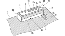
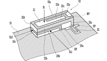
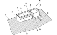
- FIG. It is a perspective view which shows the antenna 41 which concerns on 1st Embodiment, and its mounting state. It is a perspective view which shows the antenna 42 which concerns on 2nd Embodiment, and its mounting state. It is a perspective view which shows the antenna 43 which concerns on 3rd Embodiment, and its mounting state. It is a perspective view which shows the antenna 44 which concerns on 4th Embodiment, and its mounting state.
- FIG. 2 is a perspective view showing the antenna according to the first embodiment and its mounting state.
- the antenna 41 has a predetermined pattern of electrodes formed on the surface of the dielectric substrate 21.
- the dielectric substrate 21 is obtained by molding a dielectric ceramic material or a composite material of a dielectric ceramic powder and an organic material into a rectangular parallelepiped shape.
- One of the electrodes having the predetermined pattern is a radiation electrode.
- This radiation electrode is composed of a plurality of radiation electrode portions as described below.
- a radiation electrode portion 22a extending upward from the power supply end FP and a radiation electrode portion 22b connected to the radiation electrode portion 22a and extending along the upper side of the dielectric substrate 21 are respectively provided. Is formed.
- a radiation electrode portion 22c that is conductive (continuous) with the radiation electrode 22b at one edge of the dielectric substrate 21, and the upper surface of the dielectric substrate 21 continues from the radiation electrode portion 22c.
- the radiation electrode portions 22d and 22e are formed so as to circulate around the sides (peripheries).
- the radiation electrode is configured by an electrode pattern extending from the power supply end FP along the path of the radiation electrode portions 22a, (22b + 22c), 22d, and 22e.
- This radiation electrode acts as a radiation electrode with one end fed by the feed end FP and the other end open.
- the whole radiation electrode composed of the radiation electrode portions 22a, 22b, 22c, 22d, and 22e is hereinafter referred to as “radiation electrode 22”.
- the other electrode of the predetermined pattern is a branch electrode.
- the branch electrode is composed of a plurality of branch electrode portions as described below.
- a branch electrode portion 23a branched in an orthogonal direction from a branch point BP near the feeding end of the radiation electrode portion 22c, and adjacent to the branch electrode portion 23a in parallel with the radiation electrode portion 22e.
- a branch electrode portion 23b is formed.
- the entire branch electrode composed of the branch electrode portions 23a and 23b is hereinafter referred to as “branch electrode 23”.
- branch electrode 23 branched from the branch point BP near the feeding end of the radiation electrode 22 is in parallel with the vicinity of the open end of the radiation electrode 22.
- the branch electrode 23 is branched toward the point (position) where the maximum voltage of the higher mode occurs in the radiation electrode 22.
- the direction from the branch point BP of the branch electrode 23 to the tip of the branch electrode 23 and the direction from the power feed end FP of the radiation electrode 22 to the tip of the radiation electrode 22 are parallel proximity portions of the branch electrode 23 and the radiation electrode 22. Are opposite to each other. In other words, they are parallel to each other. With this structure, it is easy to obtain a capacity in the parallel proximity portion. In addition, by making the direction reverse, the direction of the current flowing through the capacitor portion becomes the same, and the current distribution on the electrode tends to be good for both the fundamental mode and the higher order mode.
- a ground electrode is formed on the circuit board 31, and an antenna 41 is mounted near the end of the circuit board 31.
- the circuit board 31 is provided with a power feeding circuit.
- the feed line 32 is a part of the feed circuit.
- the feed end of the antenna 41 is connected to the feed line 32.
- the antenna 41 is mounted on the ground electrode.
- a ground electrode non-formation region may be provided on the circuit board 31, and the antenna 41 may be mounted on the region.
- the fundamental mode is a mode in which the radiation electrode 22 resonates at a quarter wavelength.
- a voltage having a maximum voltage amplitude is distributed at the tip of the radiation electrode 22.
- the higher order mode is a mode in which the radiation electrode 22 resonates, for example, by 3/4 wavelength.
- the voltage amplitude becomes maximum at the tip of the radiation electrode 22, another point (antinode) having the maximum voltage amplitude is generated at a position near the feeding end, and the voltage amplitude is minimum between the two points having the maximum voltage amplitude.
- the voltage is distributed so that there are points (nodes).
- the voltage amplitude maximum point (antinode) near the power supply end of the higher order mode is small (at least smaller than the voltage amplitude near the open end), the voltage amplitude maximum near the power supply end of this higher order mode is the largest.
- the frequency of the higher-order mode can be set to a predetermined value with little influence on the fundamental mode.
- the higher order mode can be controlled independently of the fundamental mode by the capacity loading position with respect to the radiation electrode 22. That is, by loading a capacitor at or near the point where the maximum voltage of the higher-order mode to be used is generated, the resonance frequency of the higher-order mode can be controlled (set) in a decreasing direction.
- the resonance frequency of the fundamental mode is hardly affected. In this way, the independence of higher-order mode control is improved.
- the position of the open end of the radiation electrode 22 affects the radiation characteristics in both the fundamental mode and the higher order mode.
- the open end of the radiation electrode 22 is not particularly used for controlling the higher order mode.
- the 22 open ends can be arbitrarily arranged. Therefore, a radiation electrode having high radiation characteristics can be configured for both the fundamental mode and the higher order mode.
- the radiation electrode 22 is formed so as to circulate around the side (periphery) of the upper surface of the dielectric substrate 21, and the branch electrode 23 is formed on the upper surface of the dielectric substrate 21. 23 are formed on the same surface, and the pattern forming accuracy of both can be kept high. As a result, variations in radiation characteristics between the fundamental mode and the higher order mode can be suppressed.
- the circuit board 31 includes a wireless communication circuit, and the antenna 41 is connected to the wireless communication circuit.
- the wireless communication circuit is, for example, a high-frequency circuit unit of a mobile phone terminal.
- the circuit board 31 is accommodated in the housing of the wireless communication device.
- FIG. 3 is a perspective view showing the antenna 42 according to the second embodiment and a mounted state thereof. What is different from the antenna 41 shown in FIG. 2 in the first embodiment is the shape of the radiation electrode 22.
- radiation electrode portions 22a and 22b formed on the side surface Ss1 of the dielectric substrate 21, and radiation electrode portions 22c, 22d, 22e, and 22f formed on the upper surface St of the dielectric substrate 21;
- the radiation electrode 22 is configured.
- the open end of the radiation electrode 22 is disposed at a position further extending from the radiation electrode portion 22e parallel to the branch electrode portion 23b.
- the open end of the radiation electrode 22 can be freely arranged regardless of the position of the power supply end FP.
- FIG. 4 is a perspective view showing an antenna 43 according to the third embodiment and a mounted state thereof.
- the first embodiment is different from the antenna 41 shown in FIG. 2 in that a parasitic electrode is further provided on the dielectric substrate 21.
- the parasitic electrode portion 24a extending upward from the ground end GP on the side surface Ss1 of the dielectric substrate 21, and the parasitic electrode portion connected to the parasitic electrode portion 24a and parallel to the radiation electrode portion 22b. 24b are formed.
- the side surface Ss2 of the dielectric substrate 21 is formed with a parasitic electrode portion 24c having one end connected to the parasitic electrode portion 24b and the other end opened.
- the entirety of the parasitic electrode composed of the parasitic electrode portions 24a, 24b, and 24c is hereinafter referred to as “parasitic electrode 24”.
- the parasitic electrode 24 is coupled at a portion where the radiation electrode portion 22b and the parasitic electrode portion 24b are parallel to each other, and acts as a (another) radiation electrode different from the radiation electrode 22. Therefore, gain can be obtained in a predetermined frequency band different from the two frequency bands of the fundamental mode and the higher order mode of the radiation electrode 22.
- FIG. 5 is a perspective view showing the antenna 44 and its mounting state according to the fourth embodiment.
- a difference from the antenna 41 shown in FIG. 2 in the first embodiment is the shape of the branch electrode 23.
- the branch electrode 23 branched in the orthogonal direction from the branch point BP near the feeding end of the radiation electrode portion 22 c is formed on the upper surface St of the dielectric substrate 21. Capacitance is generated between the tip of the branch electrode 23 and a point (position) where the maximum voltage of the higher-order mode occurs in the radiation electrode 22.
- the branch electrode 23 may be opposed to a predetermined position (radiation electrode portion 22e) of the radiation electrode 22 only at the tip portion thereof.
Landscapes
- Engineering & Computer Science (AREA)
- Microelectronics & Electronic Packaging (AREA)
- Details Of Aerials (AREA)
- Support Of Aerials (AREA)
Abstract
Description
図1は特許文献1に示されているアンテナの斜視図である。図1に示すように、表面実装型のアンテナ1は、直方体状の誘電体基体2と、その誘電体基体2に形成されたループ状の放射電極3及び給電電極4とを有している。給電電極4は誘電体基体2の底面2cから側面2bに形成され、その側面2bの横側端縁領域を通って上面2aに向けて形成されている。放射電極3は、給電電極4から長方形状の上面2aの各辺の近傍領域を各辺に沿ってループ状に形成されている。このループ状の放射電極3の開放端3aは給電端部側の張り出し電極部18に所定の間隔を介して対向配置され、開放端3aと給電端部側の張り出し電極との間に容量が生じるように構成されている。
さらに、放射電極の開放端の位置により放射特性が大きな影響を受けるので、高次モード制御用の容量を形成することが、結果的に基本モード及び高次モード双方の放射特性を犠牲にする場合がある。
また、分岐電極により高次モードを制御するため、放射電極の開放端を任意に配置でき、基本モード・高次モード共に放射特性の高い放射電極を構成できる。
図2は第1の実施形態に係るアンテナ及びその実装状態を示す斜視図である。アンテナ41は、誘電体基体21の表面に所定パターンの電極が形成されたものである。誘電体基体21は、誘電体セラミックス材料、又は誘電体セラミックス粉と有機材料とのコンポジット材料が直方体形状に成形されたものである。
なお、この例ではグランド電極上にアンテナ41を実装したが、回路基板31にグランド電極非形成領域を設けて、その領域にアンテナ41を実装するようにしてもよい。
例えば基本モードは放射電極22が1/4波長共振するモードであり、この基本モードでは放射電極22の先端で電圧振幅最大となる電圧が分布する。高次モードは放射電極22が例えば3/4波長共振するモードである。この高次モードでは放射電極22の先端で電圧振幅最大となり、給電端寄りの位置にもう一つの電圧振幅最大の点(腹)が生じ、二つの電圧振幅最大の点の間に電圧振幅が最小の点(節)があるように電圧が分布する。
また、放射電極22の開放端の位置は基本モード・高次モードともに放射特性に影響を与えるが、本発明では、放射電極22の開放端を高次モードの制御に特に用いないので、放射電極22の開放端を任意に配置できる。そのため、基本モード・高次モード共に放射特性の高い放射電極を構成できる。
図3は第2の実施形態に係るアンテナ42及びその実装状態を示す斜視図である。第1の実施形態で図2に示したアンテナ41と異なるのは、放射電極22の形状である。図3に示す例では、誘電体基体21の側面Ss1に形成されている放射電極部22a,22bと、誘電体基体21の上面Stに形成されている放射電極部22c,22d,22e,22fとで放射電極22が構成されている。
このように、放射電極22の開放端は給電端FPの位置に依らずに自由に配置できる。
図4は第3の実施形態に係るアンテナ43及びその実装状態を示す斜視図である。第1の実施形態で図2に示したアンテナ41と異なるのは、誘電体基体21に無給電電極を更に設けた点である。
図5は第4の実施形態に係るアンテナ44及びその実装状態を示す斜視図である。第1の実施形態で図2に示したアンテナ41と異なるのは、分岐電極23の形状である。図5に示す例では、放射電極部22cの給電端付近の分岐点BPから直交方向に分岐した分岐電極23が誘電体基体21の上面Stに形成されている。この分岐電極23の先端と、放射電極22のうち高次モードの最大電圧が生じる点(位置)との間に容量を生じさせている。
FP…給電端
GP…接地端
Ss1,Ss2…側面
St…上面
21…誘電体基体
22…放射電極
22a,22b,22c,22d,22e,22f…放射電極部
23…分岐電極
23a…分岐電極部
23b…分岐電極部
24a,24b,24c…無給電電極部
31…回路基板
32…給電線路
41~44…アンテナ
Claims (6)
- 誘電体基体に放射電極が形成されたアンテナにおいて、
前記放射電極の第1の端部は給電端であり第2の端部は開放されていて、
前記放射電極の高次モードの最大電圧が生じる付近へ向かって前記放射電極の給電端付近の分岐点から分岐した分岐電極が前記誘電体基体に形成された、アンテナ。 - 前記分岐電極の一部と前記放射電極の開放端付近とが並行して近接した、請求項1に記載のアンテナ。
- 前記誘電体基体は直方体形状をなし、前記放射電極は、前記誘電体基体の側面を経由し、上面の辺を周回するように形成され、前記分岐電極は、前記誘電体基体の上面に形成された、請求項1又は2に記載のアンテナ。
- 前記分岐電極の前記分岐点から先端へ向かう方向と、前記放射電極の前記給電端から先端へ向かう方向とは、前記分岐電極と前記放射電極との近接部分で互いに逆向きである、請求項1乃至3の何れかに記載のアンテナ。
- 前記誘電体基体に、前記放射電極と結合する無給電電極を設けた、請求項1乃至4の何れかに記載のアンテナ。
- 請求項1乃至5の何れかに記載のアンテナと、前記アンテナが実装される回路基板と、前記回路基板を収容する筐体とを備えた無線通信装置。
Priority Applications (3)
| Application Number | Priority Date | Filing Date | Title |
|---|---|---|---|
| CN201080064041.7A CN102763276B (zh) | 2010-02-16 | 2010-10-26 | 天线及无线通信装置 |
| JP2012500450A JP5516716B2 (ja) | 2010-02-16 | 2010-10-26 | アンテナ及び無線通信装置 |
| US13/584,601 US9780441B2 (en) | 2010-02-16 | 2012-08-13 | Antenna and wireless communication device |
Applications Claiming Priority (2)
| Application Number | Priority Date | Filing Date | Title |
|---|---|---|---|
| JP2010-031249 | 2010-02-16 | ||
| JP2010031249 | 2010-02-16 |
Related Child Applications (1)
| Application Number | Title | Priority Date | Filing Date |
|---|---|---|---|
| US13/584,601 Continuation US9780441B2 (en) | 2010-02-16 | 2012-08-13 | Antenna and wireless communication device |
Publications (1)
| Publication Number | Publication Date |
|---|---|
| WO2011102017A1 true WO2011102017A1 (ja) | 2011-08-25 |
Family
ID=44482630
Family Applications (1)
| Application Number | Title | Priority Date | Filing Date |
|---|---|---|---|
| PCT/JP2010/068887 Ceased WO2011102017A1 (ja) | 2010-02-16 | 2010-10-26 | アンテナ及び無線通信装置 |
Country Status (4)
| Country | Link |
|---|---|
| US (1) | US9780441B2 (ja) |
| JP (1) | JP5516716B2 (ja) |
| CN (1) | CN102763276B (ja) |
| WO (1) | WO2011102017A1 (ja) |
Cited By (3)
| Publication number | Priority date | Publication date | Assignee | Title |
|---|---|---|---|---|
| WO2013183451A1 (ja) * | 2012-06-07 | 2013-12-12 | 株式会社村田製作所 | アンテナ装置および無線通信装置 |
| JP2015530809A (ja) * | 2013-07-31 | 2015-10-15 | ▲華▼▲為▼▲終▼端有限公司 | プリントアンテナおよび端末デバイス |
| JP2016519525A (ja) * | 2013-04-22 | 2016-06-30 | ノキア テクノロジーズ オーユー | 無線通信装置及び方法 |
Families Citing this family (5)
| Publication number | Priority date | Publication date | Assignee | Title |
|---|---|---|---|---|
| USD684564S1 (en) * | 2012-10-12 | 2013-06-18 | Avery Dennison Corporation | RFID antenna |
| USD708171S1 (en) * | 2013-03-09 | 2014-07-01 | Avery Dennison Corporation | Antenna |
| JP6478510B2 (ja) | 2013-08-20 | 2019-03-06 | キヤノン株式会社 | アンテナ |
| AU356492S (en) * | 2014-05-08 | 2014-07-15 | A passive EM antenna for an electronic device | |
| EP3503293B1 (en) * | 2017-12-19 | 2024-12-11 | Institut Mines Telecom - IMT Atlantique - Bretagne - Pays de la Loire | Configurable multiband wire antenna arrangement and design method thereof |
Citations (4)
| Publication number | Priority date | Publication date | Assignee | Title |
|---|---|---|---|---|
| JP2002158529A (ja) * | 2000-11-20 | 2002-05-31 | Murata Mfg Co Ltd | 表面実装型アンテナ構造およびそれを備えた通信機 |
| JP2004128660A (ja) * | 2002-09-30 | 2004-04-22 | Matsushita Electric Ind Co Ltd | アンテナ装置 |
| JP2004166242A (ja) * | 2002-10-23 | 2004-06-10 | Murata Mfg Co Ltd | 表面実装型アンテナおよびそれを用いたアンテナ装置および通信装置 |
| JP2007036338A (ja) * | 2005-07-22 | 2007-02-08 | Anten Corp | アンテナ |
Family Cites Families (6)
| Publication number | Priority date | Publication date | Assignee | Title |
|---|---|---|---|---|
| JP2003188637A (ja) * | 2001-12-20 | 2003-07-04 | Hitachi Cable Ltd | 平板多重アンテナおよび携帯端末 |
| AU2003281402A1 (en) * | 2002-07-05 | 2004-01-23 | Taiyo Yuden Co., Ldt. | Dielectric antenna, antenna-mounted substrate, and mobile communication machine having them therein |
| US20080266189A1 (en) * | 2007-04-24 | 2008-10-30 | Cameo Communications, Inc. | Symmetrical dual-band uni-planar antenna and wireless network device having the same |
| KR101383465B1 (ko) * | 2007-06-11 | 2014-04-10 | 삼성전자주식회사 | 휴대 단말기에 적용되는 다중대역 안테나 |
| CN101587986B (zh) * | 2008-05-19 | 2013-07-31 | 鸿富锦精密工业(深圳)有限公司 | 多频天线 |
| CN101783440B (zh) * | 2009-01-16 | 2013-03-20 | 鸿富锦精密工业(深圳)有限公司 | 多频天线 |
-
2010
- 2010-10-26 JP JP2012500450A patent/JP5516716B2/ja active Active
- 2010-10-26 CN CN201080064041.7A patent/CN102763276B/zh not_active Expired - Fee Related
- 2010-10-26 WO PCT/JP2010/068887 patent/WO2011102017A1/ja not_active Ceased
-
2012
- 2012-08-13 US US13/584,601 patent/US9780441B2/en not_active Expired - Fee Related
Patent Citations (4)
| Publication number | Priority date | Publication date | Assignee | Title |
|---|---|---|---|---|
| JP2002158529A (ja) * | 2000-11-20 | 2002-05-31 | Murata Mfg Co Ltd | 表面実装型アンテナ構造およびそれを備えた通信機 |
| JP2004128660A (ja) * | 2002-09-30 | 2004-04-22 | Matsushita Electric Ind Co Ltd | アンテナ装置 |
| JP2004166242A (ja) * | 2002-10-23 | 2004-06-10 | Murata Mfg Co Ltd | 表面実装型アンテナおよびそれを用いたアンテナ装置および通信装置 |
| JP2007036338A (ja) * | 2005-07-22 | 2007-02-08 | Anten Corp | アンテナ |
Cited By (4)
| Publication number | Priority date | Publication date | Assignee | Title |
|---|---|---|---|---|
| WO2013183451A1 (ja) * | 2012-06-07 | 2013-12-12 | 株式会社村田製作所 | アンテナ装置および無線通信装置 |
| JP2016519525A (ja) * | 2013-04-22 | 2016-06-30 | ノキア テクノロジーズ オーユー | 無線通信装置及び方法 |
| JP2015530809A (ja) * | 2013-07-31 | 2015-10-15 | ▲華▼▲為▼▲終▼端有限公司 | プリントアンテナおよび端末デバイス |
| US9847580B2 (en) | 2013-07-31 | 2017-12-19 | Huawei Device Co., Ltd. | Printed antenna and terminal device |
Also Published As
| Publication number | Publication date |
|---|---|
| CN102763276A (zh) | 2012-10-31 |
| JP5516716B2 (ja) | 2014-06-11 |
| US20120306703A1 (en) | 2012-12-06 |
| US9780441B2 (en) | 2017-10-03 |
| JPWO2011102017A1 (ja) | 2013-06-17 |
| CN102763276B (zh) | 2017-07-21 |
Similar Documents
| Publication | Publication Date | Title |
|---|---|---|
| JP5516716B2 (ja) | アンテナ及び無線通信装置 | |
| JP4632176B2 (ja) | アンテナ及び無線通信機 | |
| JP4158832B2 (ja) | アンテナ構造およびそれを備えた無線通信機 | |
| JP6351760B2 (ja) | 切り替え可能なπ字形アンテナ | |
| WO2008035526A1 (fr) | Structure d'antenne et dispositif de communication sans fil l'employant | |
| JP2005295493A (ja) | アンテナ装置 | |
| JP2010232820A (ja) | アンテナ装置 | |
| JP5440603B2 (ja) | アンテナ及び無線通信装置 | |
| JP5422587B2 (ja) | アンテナ装置 | |
| KR101043994B1 (ko) | 유전체 공진기 안테나 | |
| JP5644397B2 (ja) | 無線装置及びアンテナ装置 | |
| WO2012032975A1 (ja) | アンテナおよび移動体通信装置 | |
| JP2013211797A (ja) | 通信端末 | |
| TWI536666B (zh) | 天線 | |
| JP5626483B2 (ja) | アンテナおよび無線通信装置 | |
| JP2019016838A (ja) | アンテナ装置 | |
| JP2006060384A (ja) | 周波数可変型アンテナ及び無線通信機 | |
| JP2010130100A (ja) | マルチバンドアンテナ装置 | |
| JP2018152694A (ja) | アンテナ装置及びアンテナ装置を備えた電子機器 | |
| JP2012235422A (ja) | アンテナ装置及びこれを用いた無線モジュール並びに無線通信機器 | |
| WO2014181564A1 (ja) | アンテナ装置 | |
| WO2014188747A1 (ja) | アンテナおよび無線通信装置 | |
| JP5494310B2 (ja) | アンテナ装置 | |
| JP2010258815A (ja) | アンテナ装置 | |
| JP2009267656A (ja) | アンテナ装置及びそれを備えた無線通信装置 |
Legal Events
| Date | Code | Title | Description |
|---|---|---|---|
| WWE | Wipo information: entry into national phase |
Ref document number: 201080064041.7 Country of ref document: CN |
|
| 121 | Ep: the epo has been informed by wipo that ep was designated in this application |
Ref document number: 10846149 Country of ref document: EP Kind code of ref document: A1 |
|
| WWE | Wipo information: entry into national phase |
Ref document number: 2012500450 Country of ref document: JP |
|
| NENP | Non-entry into the national phase |
Ref country code: DE |
|
| 122 | Ep: pct application non-entry in european phase |
Ref document number: 10846149 Country of ref document: EP Kind code of ref document: A1 |