WO2011105538A1 - Procédé de fabrication d'une cellule solaire utilisant une poudre de silicium - Google Patents
Procédé de fabrication d'une cellule solaire utilisant une poudre de silicium Download PDFInfo
- Publication number
- WO2011105538A1 WO2011105538A1 PCT/JP2011/054255 JP2011054255W WO2011105538A1 WO 2011105538 A1 WO2011105538 A1 WO 2011105538A1 JP 2011054255 W JP2011054255 W JP 2011054255W WO 2011105538 A1 WO2011105538 A1 WO 2011105538A1
- Authority
- WO
- WIPO (PCT)
- Prior art keywords
- layer
- powder
- silicon
- type silicon
- conductivity type
- Prior art date
- Legal status (The legal status is an assumption and is not a legal conclusion. Google has not performed a legal analysis and makes no representation as to the accuracy of the status listed.)
- Ceased
Links
Images

Classifications
-
- H—ELECTRICITY
- H10—SEMICONDUCTOR DEVICES; ELECTRIC SOLID-STATE DEVICES NOT OTHERWISE PROVIDED FOR
- H10F—INORGANIC SEMICONDUCTOR DEVICES SENSITIVE TO INFRARED RADIATION, LIGHT, ELECTROMAGNETIC RADIATION OF SHORTER WAVELENGTH OR CORPUSCULAR RADIATION
- H10F71/00—Manufacture or treatment of devices covered by this subclass
- H10F71/121—The active layers comprising only Group IV materials
-
- C—CHEMISTRY; METALLURGY
- C23—COATING METALLIC MATERIAL; COATING MATERIAL WITH METALLIC MATERIAL; CHEMICAL SURFACE TREATMENT; DIFFUSION TREATMENT OF METALLIC MATERIAL; COATING BY VACUUM EVAPORATION, BY SPUTTERING, BY ION IMPLANTATION OR BY CHEMICAL VAPOUR DEPOSITION, IN GENERAL; INHIBITING CORROSION OF METALLIC MATERIAL OR INCRUSTATION IN GENERAL
- C23C—COATING METALLIC MATERIAL; COATING MATERIAL WITH METALLIC MATERIAL; SURFACE TREATMENT OF METALLIC MATERIAL BY DIFFUSION INTO THE SURFACE, BY CHEMICAL CONVERSION OR SUBSTITUTION; COATING BY VACUUM EVAPORATION, BY SPUTTERING, BY ION IMPLANTATION OR BY CHEMICAL VAPOUR DEPOSITION, IN GENERAL
- C23C24/00—Coating starting from inorganic powder
- C23C24/08—Coating starting from inorganic powder by application of heat or pressure and heat
- C23C24/10—Coating starting from inorganic powder by application of heat or pressure and heat with intermediate formation of a liquid phase in the layer
-
- H—ELECTRICITY
- H10—SEMICONDUCTOR DEVICES; ELECTRIC SOLID-STATE DEVICES NOT OTHERWISE PROVIDED FOR
- H10F—INORGANIC SEMICONDUCTOR DEVICES SENSITIVE TO INFRARED RADIATION, LIGHT, ELECTROMAGNETIC RADIATION OF SHORTER WAVELENGTH OR CORPUSCULAR RADIATION
- H10F10/00—Individual photovoltaic cells, e.g. solar cells
- H10F10/10—Individual photovoltaic cells, e.g. solar cells having potential barriers
- H10F10/14—Photovoltaic cells having only PN homojunction potential barriers
-
- Y—GENERAL TAGGING OF NEW TECHNOLOGICAL DEVELOPMENTS; GENERAL TAGGING OF CROSS-SECTIONAL TECHNOLOGIES SPANNING OVER SEVERAL SECTIONS OF THE IPC; TECHNICAL SUBJECTS COVERED BY FORMER USPC CROSS-REFERENCE ART COLLECTIONS [XRACs] AND DIGESTS
- Y02—TECHNOLOGIES OR APPLICATIONS FOR MITIGATION OR ADAPTATION AGAINST CLIMATE CHANGE
- Y02E—REDUCTION OF GREENHOUSE GAS [GHG] EMISSIONS, RELATED TO ENERGY GENERATION, TRANSMISSION OR DISTRIBUTION
- Y02E10/00—Energy generation through renewable energy sources
- Y02E10/50—Photovoltaic [PV] energy
- Y02E10/547—Monocrystalline silicon PV cells
-
- Y—GENERAL TAGGING OF NEW TECHNOLOGICAL DEVELOPMENTS; GENERAL TAGGING OF CROSS-SECTIONAL TECHNOLOGIES SPANNING OVER SEVERAL SECTIONS OF THE IPC; TECHNICAL SUBJECTS COVERED BY FORMER USPC CROSS-REFERENCE ART COLLECTIONS [XRACs] AND DIGESTS
- Y02—TECHNOLOGIES OR APPLICATIONS FOR MITIGATION OR ADAPTATION AGAINST CLIMATE CHANGE
- Y02P—CLIMATE CHANGE MITIGATION TECHNOLOGIES IN THE PRODUCTION OR PROCESSING OF GOODS
- Y02P70/00—Climate change mitigation technologies in the production process for final industrial or consumer products
- Y02P70/50—Manufacturing or production processes characterised by the final manufactured product
Definitions
- the present invention relates to a method for producing a silicon solar battery cell using silicon powder as a raw material.
- a single crystal silicon type, a polycrystalline silicon type, a microcrystalline silicon type, an amorphous silicon type, and the like are known as types of silicon solar cells.
- a high-purity silicon wafer is used as a semiconductor substrate, or a silicon film is formed on an insulating or conductive substrate using a CVD method or a vapor deposition method to form a PN junction or a PIN junction.
- An object of the present invention is to provide a method of manufacturing a solar battery cell capable of mass-producing solar battery cells by a simple process and at a low cost.
- the method for producing a solar battery cell of the present invention provides a silicon powder of a first conductivity type, arranges the powder in a layer form to form a silicon powder layer, and heats the powder layer above the melting point of silicon.
- the first conductivity type silicon layer is formed by melting and cooling, a second conductivity type silicon powder is prepared, and the powder is arranged in layers on the first conductivity type silicon layer.
- a two-conductivity type silicon powder layer is formed and heated to a temperature equal to or higher than the melting point of silicon, whereby the powder layer is melted and cooled to form a second-conductivity type silicon layer.
- the method for manufacturing a photovoltaic cell prepares a first silicon powder, arranges the powder in layers, forms a silicon powder layer, and compresses the powder layer by applying heat and pressure. Then, firing is performed to form a first conductivity type silicon layer, a second silicon powder is prepared, and the powder is arranged on the first conductivity type silicon layer to form a second silicon powder layer. Then, by applying heat and pressure, the powder layer is fired while being compressed to form a second conductivity type silicon layer.
- solar cells can be manufactured from silicon powder.
- a first conductive type silicon powder layer is formed, and heat is applied to melt and cool the powder layer, thereby forming a first conductive type silicon layer, and a second conductive type silicon layer is formed on the silicon layer.
- the powder layer is melted and cooled to form a second conductivity type silicon layer. Therefore, solar cells with a PN junction can be easily and continuously formed.
- the powder layer may be fired while being compressed by applying heat and pressure.
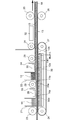
- FIG. 1 is a cross-sectional view of a solar cell manufacturing apparatus according to a first embodiment of the present invention.
- FIG. 4 is a cross-sectional view of a solar cell manufacturing apparatus according to a second embodiment of the present invention.
- P-type silicon powder 11 and N-type silicon powder 12 are prepared.
- the silicon particles of these powders 11 and 12 are substantially spherical, have a particle size of about 0.1-10 ⁇ m, and have a solar cell grade (7 nine level) purity.
- These powders 11 and 12 can be mass-produced by a method for producing high-purity silicon using a rotating crucible of the present inventors (Japanese Patent Application No. 2010-35714).
- the P-type silicon powder 11 is accommodated in the storage unit 21, and the N-type silicon powder 12 is stored in the storage unit 22.
- a transparent insulating foil 13 and a transparent electrode foil 14 bonded thereto are fixed on the plate 35 by rollers 23, 24, 25, 26 and a heat-resistant metal belt 27 at a constant speed below the reservoirs 21 and 22. Sent in the direction. Openings 21 a and 22 a are provided below the storage portions 21 and 22, and the layers are disposed in layers on the transparent electrode foil 14 in which the P-type silicon powder 11 is bonded onto the transparent insulating foil 13 from the opening 21 a.
- the P-type silicon powder layer 11a arranged in layers on the transparent electrode foil 14 is sent in the direction of the arrow in the figure, and heat is applied directly under the heater 28, which is lower than the melting point of silicon (1412 ° C.) 600-1350. Heated to ° C. Then, pressure is applied by the rolling roller 29, and the P-type silicon powder layer 11a in a heated state is fired while being pressed. Thus, by applying heat and pressure, the P-type silicon powder layer 11a is baked while being compressed, and the P-type silicon powder layer 11a becomes a P-type silicon layer 11b which is pressure-sintered.
- silicon particles having a particle size of about 0.1-10 ⁇ m are bonded to each other by diffusion bonding, and a strong bonded state is formed both electrically and mechanically.
- the N-type silicon powder 12 When the P-type silicon layer 11b moves below the reservoir 22, the N-type silicon powder 12 is disposed on the P-type silicon layer 11b, and when the P-type silicon layer 11b passes through the opening 22a, the N-type silicon powder layer 12a becomes the P-type silicon layer 11b. Formed in layers on top. Then, heat is applied directly under the heater 30, heated to 600 to 1350 ° C., and pressure is applied by the rolling roller 31. As a result, the N-type silicon powder layer 12a is baked while being compressed to become a pressure-sintered N-type silicon layer 12b, and the silicon particles are bonded to each other by diffusion bonding. At the same time, the silicon particles of the P-type silicon layer 11b are also bonded by diffusion bonding, and a PN junction is formed at the interface between both layers.
- An electrode foil (aluminum foil or copper foil or the like) 15 is disposed on the upper surface side of the N-type silicon layer 12b, and is joined to the upper surface of the N-type silicon layer 12b by heating with a heater 32. As a result, a PN junction is formed between the P-type silicon layer 11b and the N-type silicon layer 12b, and both the layers 11b and 12b are sandwiched between the two electrode foils 13 and 15, and are formed on the transparent insulating foil 13. Fixed solar cells are continuously formed.
- the manufacturing process of the solar cell is preferably performed in an inert gas atmosphere such as vacuum or Ar.
- the said Example uses the P-type silicon powder 11 and the N-type silicon powder 12 which were doped beforehand as a raw material.
- non-doped silicon powder may be used as a raw material
- a dopant may be added from the dopant inlets 33 and 34
- the P-type or N-type may be doped in the process of pressure firing.
- an I-type silicon layer obtained by pressure-sintering non-doped silicon powder may be provided between the P-type silicon layer 11b and the N-type silicon layer 12b to form a PIN-type junction.
- a P-type silicon powder 11 and an N-type silicon powder 12 are prepared, and a transparent insulating foil 13 and a transparent electrode foil 14 bonded to the rollers 23 and 22 are stored at a constant speed below the storage portions 21 and 22 containing these. It is the same as in the first embodiment that 24, 25, 26 and the belt 27 are sent on the plate 35 in the direction of the arrow in the figure. Accordingly, the P-type silicon powder layer 11a is formed in layers on the transparent electrode foil 14 bonded on the transparent insulating foil 13 from the opening 21a, and the N-type silicon powder layer 12a is formed in layers on the P-type silicon layer 11b from the opening 22a. It is formed.
- the powder layer 11a When the P-type silicon powder layer 11a enters under the heater 41, the powder layer 11a is preheated to 1300 to 1400 ° C., and is heated to 1500 ° C., which is equal to or higher than the melting point (1420 ° C.) of silicon. It is heated above. As a result, the temperature of the powder layer 11a gradually rises due to preheating, bubbles and the like are removed, and the powder layer 11a is melted to exceed the melting point by laser irradiation to be in a liquid state. And it cools with the liquid nitrogen or the water cooling roll 43, and becomes the solid-phase P-type silicon layer 11b. In the P-type silicon layer 11b, silicon is monocrystalline, polycrystalline, or amorphous.
- an N-type silicon powder layer 12a is formed in a layered manner on the P-type silicon layer 11b in the reservoir 22 of the N-type silicon powder 12. Then, in the same manner as described above, preheating is performed by the heater 44, melting is performed by laser irradiation of the laser irradiation device 45, and the liquid phase state is obtained. The cooling roll 46 cools the solid phase N-type silicon layer 12b. At the same time, a PN junction is formed at the interface between the P-type silicon layer 12a and the N-type silicon layer 12b.
- the plate 35 includes a water cooling pipe 35a and a vacuum suction pipe 35b.
- the insulating foil 13 and the electrode foil 14 are cooled by cooling water in the water cooling pipe 35a while adsorbing the insulating foil 13 and the electrode foil 14 by the vacuum suction pipe 35b. Cool down. Therefore, even if the silicon powder layers 11a and 12a are formed on the electrode foil 14 bonded to the insulating foil 13, and the silicon powder layers 11a and 12a are heated at a temperature of 1500 ° C. or more by laser irradiation, the insulating foil 13 and the electrode The temperature of the foil 14 is kept at the temperature of the cooling water and they are not damaged.
- the electrode foil 15 can be tightly fixed to the N-type silicon layer 12b by placing the electrode foil 15 on the upper portion after the formation of the N-type silicon layer 12b and heating it with the heater 32.
- a solar battery cell having P-type and N-type silicon layers 11b and 12b between 15 can be formed by a simple process.
- the present invention enables the production of solar cells from silicon powder. Thereby, a photovoltaic cell can be mass-produced with a simple process and low cost.
Landscapes
- Chemical & Material Sciences (AREA)
- Chemical Kinetics & Catalysis (AREA)
- Engineering & Computer Science (AREA)
- Materials Engineering (AREA)
- Mechanical Engineering (AREA)
- Metallurgy (AREA)
- Organic Chemistry (AREA)
- Photovoltaic Devices (AREA)
- Silicon Compounds (AREA)
Abstract
L'invention concerne un procédé de fabrication d'une cellule solaire qui permet la production de masse, simple et bon marché de cellules solaires. Une poudre de silicium d'un premier type de conductivité (11) est préparée, une couche de poudre de silicium (11a) est formée en déposant la poudre sous la forme d'une couche, la couche de poudre est fondue en la chauffant jusqu'au point de fusion du silicium ou plus, et une couche de silicium d'un premier type de conductivité (11b) est formée en refroidissant la couche fondue. Une poudre de silicium d'un deuxième type de conductivité (12) est préparée, une couche de poudre de silicium d'un deuxième type de conductivité (12a) est formée en déposant la poudre sous la forme d'une couche sur la couche de silicium d'un premier type de conductivité (11b), la couche de poudre est fondue en la chauffant jusqu'au point de fusion du silicium ou plus, et une couche de silicium d'un deuxième type de conductivité (12b) est formée en refroidissant la couche fondue.
Priority Applications (4)
| Application Number | Priority Date | Filing Date | Title |
|---|---|---|---|
| CN201180010870.1A CN102834926B (zh) | 2010-02-25 | 2011-02-25 | 使用了硅粉末的太阳能电池单体的制造方法 |
| EP11747494.0A EP2541616B1 (fr) | 2010-02-25 | 2011-02-25 | Procédé de fabrication d'une cellule solaire utilisant une poudre de silicium |
| JP2012501876A JP5761172B2 (ja) | 2010-02-25 | 2011-02-25 | シリコン粉末を用いた太陽電池セルの製造方法 |
| US13/591,628 US8603850B2 (en) | 2010-02-25 | 2012-08-22 | Method for manufacturing solar cell using silicon powder |
Applications Claiming Priority (2)
| Application Number | Priority Date | Filing Date | Title |
|---|---|---|---|
| JP2010-039497 | 2010-02-25 | ||
| JP2010039497 | 2010-02-25 |
Related Child Applications (1)
| Application Number | Title | Priority Date | Filing Date |
|---|---|---|---|
| US13/591,628 Continuation US8603850B2 (en) | 2010-02-25 | 2012-08-22 | Method for manufacturing solar cell using silicon powder |
Publications (1)
| Publication Number | Publication Date |
|---|---|
| WO2011105538A1 true WO2011105538A1 (fr) | 2011-09-01 |
Family
ID=44506935
Family Applications (1)
| Application Number | Title | Priority Date | Filing Date |
|---|---|---|---|
| PCT/JP2011/054255 Ceased WO2011105538A1 (fr) | 2010-02-25 | 2011-02-25 | Procédé de fabrication d'une cellule solaire utilisant une poudre de silicium |
Country Status (5)
| Country | Link |
|---|---|
| US (1) | US8603850B2 (fr) |
| EP (1) | EP2541616B1 (fr) |
| JP (1) | JP5761172B2 (fr) |
| CN (1) | CN102834926B (fr) |
| WO (1) | WO2011105538A1 (fr) |
Families Citing this family (3)
| Publication number | Priority date | Publication date | Assignee | Title |
|---|---|---|---|---|
| TWI901741B (zh) * | 2020-08-28 | 2025-10-21 | 日商東京威力科創股份有限公司 | 電漿耐受部件的製造方法 |
| US11764315B2 (en) * | 2020-09-16 | 2023-09-19 | Maxeon Solar Pte. Ltd. | Solar cell separation with edge coating |
| CN115224238B (zh) * | 2022-09-20 | 2022-11-29 | 河南锂动电源有限公司 | 一种锂离子电池负极极片及其制作方法和激光碳化装置 |
Citations (3)
| Publication number | Priority date | Publication date | Assignee | Title |
|---|---|---|---|---|
| JP2002151713A (ja) * | 2000-08-29 | 2002-05-24 | Kyocera Corp | 太陽電池素子基板及びその製造方法 |
| JP2009246041A (ja) * | 2008-03-28 | 2009-10-22 | Mitsubishi Electric Corp | 太陽電池およびその製造方法 |
| JP2010035714A (ja) | 2008-08-01 | 2010-02-18 | Canon Inc | X線画像診断装置および制御方法 |
Family Cites Families (17)
| Publication number | Priority date | Publication date | Assignee | Title |
|---|---|---|---|---|
| DE3035563C2 (de) * | 1980-09-20 | 1984-10-11 | Licentia Patent-Verwaltungs-Gmbh, 6000 Frankfurt | Verfahren zum Herstellen einer polykristallinen Silizium-Solarzelle |
| DE3536743C2 (de) * | 1985-10-15 | 1994-11-10 | Siemens Ag | Verfahren zum Herstellung von großflächigen Siliziumkristallkörpern für Solarzellen |
| JPH06268242A (ja) * | 1993-03-17 | 1994-09-22 | Matsushita Electric Ind Co Ltd | シリコン基板の製造方法および結晶質シリコン太陽電池 |
| AU676330B2 (en) * | 1993-06-11 | 1997-03-06 | Isovolta Osterreichische Isolierstoffwerke Aktiengesellschaft | Process and device for manufacturing photovoltaic modules |
| DE19652818A1 (de) * | 1996-12-18 | 1998-07-02 | Priesemuth W | Verfahren zum Herstellen einer Solarzelle sowie Solarzelle |
| EP0978146A4 (fr) * | 1997-03-04 | 2000-08-09 | Astropower Inc | Substrat polycristallin a grain columnaire pour cellule photovoltaique et perfectionnement du procede de fabrication |
| JP2001250967A (ja) * | 2000-03-03 | 2001-09-14 | Canon Inc | 光起電力素子及び光起電力素子の製造方法 |
| JP4140247B2 (ja) * | 2002-03-04 | 2008-08-27 | 独立行政法人産業技術総合研究所 | シート型β−FeSi2素子 |
| DE10239845C1 (de) * | 2002-08-29 | 2003-12-24 | Day4 Energy Inc | Elektrode für fotovoltaische Zellen, fotovoltaische Zelle und fotovoltaischer Modul |
| US8192648B2 (en) * | 2003-04-14 | 2012-06-05 | S'tile | Method for forming a sintered semiconductor material |
| US8405183B2 (en) * | 2003-04-14 | 2013-03-26 | S'Tile Pole des Eco-Industries | Semiconductor structure |
| WO2008137738A2 (fr) * | 2007-05-03 | 2008-11-13 | Innovalight, Inc. | Procédé de fabrication de jonctions de semi-conducteur du groupe iv en utilisant un traitement au laser |
| JP4990738B2 (ja) * | 2007-11-09 | 2012-08-01 | 株式会社ブリヂストン | 太陽電池の製造方法 |
| US20090208770A1 (en) * | 2008-02-14 | 2009-08-20 | Ralf Jonczyk | Semiconductor sheets and methods for fabricating the same |
| US20090280336A1 (en) * | 2008-05-08 | 2009-11-12 | Ralf Jonczyk | Semiconductor sheets and methods of fabricating the same |
| JP2010206161A (ja) * | 2009-02-04 | 2010-09-16 | Sony Corp | 成膜方法および半導体装置の製造方法 |
| JP2011116616A (ja) | 2009-10-29 | 2011-06-16 | Sanki Dengyo Kk | 回転ルツボ装置を用いた高純度シリコンの製造方法 |
-
2011
- 2011-02-25 EP EP11747494.0A patent/EP2541616B1/fr not_active Not-in-force
- 2011-02-25 CN CN201180010870.1A patent/CN102834926B/zh not_active Expired - Fee Related
- 2011-02-25 WO PCT/JP2011/054255 patent/WO2011105538A1/fr not_active Ceased
- 2011-02-25 JP JP2012501876A patent/JP5761172B2/ja not_active Expired - Fee Related
-
2012
- 2012-08-22 US US13/591,628 patent/US8603850B2/en not_active Expired - Fee Related
Patent Citations (3)
| Publication number | Priority date | Publication date | Assignee | Title |
|---|---|---|---|---|
| JP2002151713A (ja) * | 2000-08-29 | 2002-05-24 | Kyocera Corp | 太陽電池素子基板及びその製造方法 |
| JP2009246041A (ja) * | 2008-03-28 | 2009-10-22 | Mitsubishi Electric Corp | 太陽電池およびその製造方法 |
| JP2010035714A (ja) | 2008-08-01 | 2010-02-18 | Canon Inc | X線画像診断装置および制御方法 |
Non-Patent Citations (1)
| Title |
|---|
| See also references of EP2541616A4 |
Also Published As
| Publication number | Publication date |
|---|---|
| EP2541616B1 (fr) | 2016-05-04 |
| JP5761172B2 (ja) | 2015-08-12 |
| EP2541616A4 (fr) | 2014-01-29 |
| US20130045559A1 (en) | 2013-02-21 |
| EP2541616A1 (fr) | 2013-01-02 |
| JPWO2011105538A1 (ja) | 2013-06-20 |
| US8603850B2 (en) | 2013-12-10 |
| CN102834926A (zh) | 2012-12-19 |
| CN102834926B (zh) | 2015-07-22 |
Similar Documents
| Publication | Publication Date | Title |
|---|---|---|
| JP4869061B2 (ja) | 焼結された半導体材料 | |
| CN102893408B (zh) | 光伏器件导电层 | |
| US9493358B2 (en) | Photovoltaic module including integrated photovoltaic cells | |
| CN121442831A (zh) | 一种单太阳能电池和电池组件 | |
| JPWO2011048797A1 (ja) | 結晶型太陽電池パネルの製造方法 | |
| JP5761172B2 (ja) | シリコン粉末を用いた太陽電池セルの製造方法 | |
| US8420515B2 (en) | Method of producing a solar cell | |
| US11152556B2 (en) | Flexible and conformable thermoelectric compositions | |
| TW202143514A (zh) | 熱電變換體、熱電變換模組、及熱電變換體之製造方法 | |
| US4602422A (en) | Flash compression process for making photovoltaic cells | |
| TWI905277B (zh) | 熱電轉換材料層 | |
| TWI506807B (zh) | 太陽能電池製造方法 | |
| JP4869196B2 (ja) | 回転式拡散装置および光電変換装置の製造方法 | |
| JP2013177264A (ja) | Si微細粒子による薄膜層の形成方法、半導体装置および半導体装置の製造方法、並びに太陽電池および太陽電池の製造方法。 | |
| JP2006156584A (ja) | 結晶シリコン粒子への不純物の拡散方法および光電変換装置ならびに光発電装置 | |
| JP4869195B2 (ja) | 光電変換装置の製造方法 | |
| US9741881B2 (en) | Photovoltaic module including integrated photovoltaic cells | |
| Shengrong et al. | Progress in Preparation and Performance Optimization of 3D/2D Halide Perovskite Heterojunction | |
| JP2025154931A (ja) | 熱電ウェハ | |
| WO2015063689A1 (fr) | Substrat composite a base de silicium presentant des zones actives separees par des zones d'isolation electrique comportant un feuillard en carbure de silicium | |
| WO2019155019A1 (fr) | Couche de silicium sur couche d'aluminium riche en silicium | |
| JP2007173425A (ja) | 光電変換装置の製造方法および光発電装置 | |
| JPS5946110B2 (ja) | シリコンタイヨウデンチノセイゾウホウホウ | |
| JP2012017234A (ja) | 半導体粒子の製造方法 | |
| JP2008300511A (ja) | 光電変換装置 |
Legal Events
| Date | Code | Title | Description |
|---|---|---|---|
| WWE | Wipo information: entry into national phase |
Ref document number: 201180010870.1 Country of ref document: CN |
|
| 121 | Ep: the epo has been informed by wipo that ep was designated in this application |
Ref document number: 11747494 Country of ref document: EP Kind code of ref document: A1 |
|
| WWE | Wipo information: entry into national phase |
Ref document number: 2012501876 Country of ref document: JP |
|
| NENP | Non-entry into the national phase |
Ref country code: DE |
|
| WWE | Wipo information: entry into national phase |
Ref document number: 2011747494 Country of ref document: EP |