WO2011121845A1 - Appareil d'éclairage et appareil de culture de plantes - Google Patents
Appareil d'éclairage et appareil de culture de plantes Download PDFInfo
- Publication number
- WO2011121845A1 WO2011121845A1 PCT/JP2010/071276 JP2010071276W WO2011121845A1 WO 2011121845 A1 WO2011121845 A1 WO 2011121845A1 JP 2010071276 W JP2010071276 W JP 2010071276W WO 2011121845 A1 WO2011121845 A1 WO 2011121845A1
- Authority
- WO
- WIPO (PCT)
- Prior art keywords
- light
- lens
- fixing plate
- plant
- led
- Prior art date
- Legal status (The legal status is an assumption and is not a legal conclusion. Google has not performed a legal analysis and makes no representation as to the accuracy of the status listed.)
- Ceased
Links
Images




Classifications
-
- F—MECHANICAL ENGINEERING; LIGHTING; HEATING; WEAPONS; BLASTING
- F21—LIGHTING
- F21V—FUNCTIONAL FEATURES OR DETAILS OF LIGHTING DEVICES OR SYSTEMS THEREOF; STRUCTURAL COMBINATIONS OF LIGHTING DEVICES WITH OTHER ARTICLES, NOT OTHERWISE PROVIDED FOR
- F21V5/00—Refractors for light sources
- F21V5/007—Array of lenses or refractors for a cluster of light sources, e.g. for arrangement of multiple light sources in one plane
-
- A—HUMAN NECESSITIES
- A01—AGRICULTURE; FORESTRY; ANIMAL HUSBANDRY; HUNTING; TRAPPING; FISHING
- A01G—HORTICULTURE; CULTIVATION OF VEGETABLES, FLOWERS, RICE, FRUIT, VINES, HOPS OR SEAWEED; FORESTRY; WATERING
- A01G7/00—Botany in general
- A01G7/04—Electric or magnetic or acoustic treatment of plants for promoting growth
- A01G7/045—Electric or magnetic or acoustic treatment of plants for promoting growth with electric lighting
-
- A—HUMAN NECESSITIES
- A01—AGRICULTURE; FORESTRY; ANIMAL HUSBANDRY; HUNTING; TRAPPING; FISHING
- A01G—HORTICULTURE; CULTIVATION OF VEGETABLES, FLOWERS, RICE, FRUIT, VINES, HOPS OR SEAWEED; FORESTRY; WATERING
- A01G9/00—Cultivation in receptacles, forcing-frames or greenhouses; Edging for beds, lawn or the like
- A01G9/24—Devices or systems for heating, ventilating, regulating temperature, illuminating, or watering, in greenhouses, forcing-frames, or the like
- A01G9/249—Lighting means
-
- F—MECHANICAL ENGINEERING; LIGHTING; HEATING; WEAPONS; BLASTING
- F21—LIGHTING
- F21V—FUNCTIONAL FEATURES OR DETAILS OF LIGHTING DEVICES OR SYSTEMS THEREOF; STRUCTURAL COMBINATIONS OF LIGHTING DEVICES WITH OTHER ARTICLES, NOT OTHERWISE PROVIDED FOR
- F21V17/00—Fastening of component parts of lighting devices, e.g. shades, globes, refractors, reflectors, filters, screens, grids or protective cages
- F21V17/002—Fastening of component parts of lighting devices, e.g. shades, globes, refractors, reflectors, filters, screens, grids or protective cages with provision for interchangeability, i.e. component parts being especially adapted to be replaced by another part with the same or a different function
-
- F—MECHANICAL ENGINEERING; LIGHTING; HEATING; WEAPONS; BLASTING
- F21—LIGHTING
- F21V—FUNCTIONAL FEATURES OR DETAILS OF LIGHTING DEVICES OR SYSTEMS THEREOF; STRUCTURAL COMBINATIONS OF LIGHTING DEVICES WITH OTHER ARTICLES, NOT OTHERWISE PROVIDED FOR
- F21V17/00—Fastening of component parts of lighting devices, e.g. shades, globes, refractors, reflectors, filters, screens, grids or protective cages
- F21V17/10—Fastening of component parts of lighting devices, e.g. shades, globes, refractors, reflectors, filters, screens, grids or protective cages characterised by specific fastening means or way of fastening
- F21V17/12—Fastening of component parts of lighting devices, e.g. shades, globes, refractors, reflectors, filters, screens, grids or protective cages characterised by specific fastening means or way of fastening by screwing
-
- F—MECHANICAL ENGINEERING; LIGHTING; HEATING; WEAPONS; BLASTING
- F21—LIGHTING
- F21Y—INDEXING SCHEME ASSOCIATED WITH SUBCLASSES F21K, F21L, F21S and F21V, RELATING TO THE FORM OR THE KIND OF THE LIGHT SOURCES OR OF THE COLOUR OF THE LIGHT EMITTED
- F21Y2105/00—Planar light sources
- F21Y2105/10—Planar light sources comprising a two-dimensional [2D] array of point-like light-generating elements
-
- F—MECHANICAL ENGINEERING; LIGHTING; HEATING; WEAPONS; BLASTING
- F21—LIGHTING
- F21Y—INDEXING SCHEME ASSOCIATED WITH SUBCLASSES F21K, F21L, F21S and F21V, RELATING TO THE FORM OR THE KIND OF THE LIGHT SOURCES OR OF THE COLOUR OF THE LIGHT EMITTED
- F21Y2115/00—Light-generating elements of semiconductor light sources
- F21Y2115/10—Light-emitting diodes [LED]
-
- Y—GENERAL TAGGING OF NEW TECHNOLOGICAL DEVELOPMENTS; GENERAL TAGGING OF CROSS-SECTIONAL TECHNOLOGIES SPANNING OVER SEVERAL SECTIONS OF THE IPC; TECHNICAL SUBJECTS COVERED BY FORMER USPC CROSS-REFERENCE ART COLLECTIONS [XRACs] AND DIGESTS
- Y02—TECHNOLOGIES OR APPLICATIONS FOR MITIGATION OR ADAPTATION AGAINST CLIMATE CHANGE
- Y02A—TECHNOLOGIES FOR ADAPTATION TO CLIMATE CHANGE
- Y02A40/00—Adaptation technologies in agriculture, forestry, livestock or agroalimentary production
- Y02A40/10—Adaptation technologies in agriculture, forestry, livestock or agroalimentary production in agriculture
- Y02A40/25—Greenhouse technology, e.g. cooling systems therefor
-
- Y—GENERAL TAGGING OF NEW TECHNOLOGICAL DEVELOPMENTS; GENERAL TAGGING OF CROSS-SECTIONAL TECHNOLOGIES SPANNING OVER SEVERAL SECTIONS OF THE IPC; TECHNICAL SUBJECTS COVERED BY FORMER USPC CROSS-REFERENCE ART COLLECTIONS [XRACs] AND DIGESTS
- Y02—TECHNOLOGIES OR APPLICATIONS FOR MITIGATION OR ADAPTATION AGAINST CLIMATE CHANGE
- Y02P—CLIMATE CHANGE MITIGATION TECHNOLOGIES IN THE PRODUCTION OR PROCESSING OF GOODS
- Y02P60/00—Technologies relating to agriculture, livestock or agroalimentary industries
- Y02P60/14—Measures for saving energy, e.g. in green houses
Definitions
- the present invention relates to a lighting device for plant cultivation and a plant cultivation device equipped with the same.
- Lighting devices using light emitting diodes (LEDs) as light sources have recently been used in various fields. As an example, it has been proposed to use an LED lighting device as an artificial light source for a plant factory or a plant cultivation apparatus for cultivating plants such as vegetables indoors.
- LEDs light emitting diodes
- the LED is not only efficient as an illumination light source for plants in that only light having a wavelength necessary for plants can be freely selected, but also conventional lamps such as incandescent lamps, fluorescent lamps, metal halide lamps, and high-pressure sodium lamps. It is very advantageous as a light source for plant cultivation because it does not contain infrared rays and heat rays contained in a large amount in the light source. In other words, in the conventional light source, direct illumination from the vicinity of the cultivated plant is impossible in order to avoid troubles such as leaf burning by heat rays (that is, an expensive and large space heat removal device is required), and the light utilization efficiency Was disadvantageous.
- Patent Documents 1 to 3 propose a technique of using an illumination device using LEDs as a light source for plant cultivation.
- the LED light source does not generate heat rays unlike the conventional light source, but a part of the input electric power is not converted into light, leading to a temperature rise (that is, heat generation) of the LED element itself. .
- Such heat generation of the LED may reach about 40 ° C. to 80 ° C. at the surface temperature of the LED package, which is not preferable for plant cultivation.
- the temperature rise of the LED element is not preferable because it leads to deterioration of performance for the LED element itself. Therefore, it is desired to take some measures to dissipate heat from the LED element and the LED substrate.
- Patent Document 1 proposes a plant cultivation apparatus that includes a panel-shaped LED light source and a cooling device for cooling the LED.
- power consumption can be suppressed by using the LED as a light source, and a temperature rise of the LED itself is suppressed by providing a cooling device.
- Japanese Patent Publication “JP 9-98665 A (published on April 15, 1997)” Japanese Patent Publication “JP 2005-185823 (July 14, 2005)” Japanese Patent Publication “Japanese Patent Laid-Open No. 2008-142030 (published on June 26, 2008)”
- a conventional lighting device using an LED as a light source does not have a configuration in which the intensity distribution in each direction of light emitted from the LED (these are referred to as “light distribution” of the LED) can be adjusted.
- the present invention has been made in view of the above problems, and an object of the present invention is to provide an illuminating device for plant cultivation that has been improved from the viewpoints of heat generation control of LED and light distribution adjustment of LED.
- an illumination device that irradiates light to a plant, and includes a light-emitting diode as a light source, a substrate on which the light-emitting diodes are arranged, and the substrate. And an optical member that changes the optical path of the irradiation light from the light-emitting diode, and the optical member is attached to the apparatus in a state where it can be attached and detached. It is characterized by being.
- an optical member that can change the optical path of light from the light emitting diode is attached to the device in a detachable state.
- “changing the optical path” means changing the irradiation range and irradiation direction of light from the state emitted from the light source.
- the expression “changing the light path of the light emitting diode” can be rephrased as “adjusting the light distribution of the light emitting diode”.
- the irradiation range and irradiation direction of the light irradiated from the light emitting diode can be changed by replacing optical members having different characteristics according to the purpose. Therefore, according to the illuminating device of the present invention, it is possible to perform efficient light irradiation according to the type of plant to be irradiated and the growth state.
- an optical member is provided between the plant and the substrate on which the light emitting diodes are arranged.
- it can be set as the structure where the heat which generate
- the optical member absorbs heat generated from the surface of the light emitting diode and the substrate, and can be efficiently radiated. Therefore, the cooling effect of the light emitting diode can be further enhanced as compared with the conventional configuration in which only the cooling plate is provided on the back surface of the substrate.
- the optical member is provided between the plant and the light emitting diode installation substrate, the area in contact with the outside air on the substrate on which the light emitting diode is mounted is reduced. For this reason, even if a temperature difference occurs between the space where the plant is placed and the light emitting diode, and the condensation occurs, the substrate is not easily cooled by the outside air, and the light emitting diode is less likely to cause the condensation. it can. Therefore, the light emitting diode is not damaged by condensation, and the reliability of the light emitting diode can be improved and the life of the light emitting diode can be extended.
- the plant cultivation apparatus according to the present invention includes any one of the above-described lighting apparatuses.
- the plant cultivation apparatus of the present invention can change the irradiation range and irradiation direction of the light emitted from the light emitting diode according to the purpose. Moreover, in the plant cultivation apparatus of this invention, it can be set as the structure where the heat
- the optical member is provided between the plant and the light emitting diode installation substrate, so that a temperature difference occurs between the space where the plant is disposed and the light emitting diode, thereby causing dew condensation. Even when this occurs, the light-emitting diode can have a structure in which condensation does not easily occur. Therefore, the light emitting diode is not damaged by condensation, and the reliability of the light emitting diode can be improved and the life of the light emitting diode can be extended.
- the light distribution adjustment of the light emitting diode can be easily performed by replacing the optical member according to the application. Further, by providing an optical member between the light emitting die auto and the plant, it is possible to realize a structure in which the plant is not easily affected by the heat generated by the light emitting diode and a structure in which condensation is unlikely to occur in the light emitting diode.
- FIG. (A)-(d) is sectional drawing which shows the specific example of the structure of the lens with which the illuminating device concerning one embodiment of this invention was equipped.
- FIG. 11B is a plan view of a lens fixing plate and a heat conductive sheet provided in the lighting device shown in FIG. 10.
- C is sectional drawing which expands and shows a part of illuminating device shown to (a) further.
- FIGS. 1 to 9 An embodiment of the present invention will be described with reference to FIGS. 1 to 9 as follows. However, the dimensions, materials, shapes, relative arrangements, and the like of the components described in this embodiment are not intended to limit the scope of the present invention only to those unless otherwise specified. This is just an example.
- the plant cultivation device 10 is configured by a rectangular parallelepiped case 11, and an illumination device 12 is provided on the upper surface of the case 11.
- the plant 31 is placed on the bottom surface of the case 11, and light is irradiated from the lighting device 12 provided on the top surface.
- the shape of the case 11 is not limited to a rectangular parallelepiped shape as shown in FIG. Examples of other shapes include a shape like a shelf composed of a plurality of stages, a cylindrical shelf, a doll bed, and the like.
- the arrangement position of the lighting device 12 is not necessarily limited to the upper surface, and it is only necessary that the plant placed in the case 11 can be irradiated with light.
- FIG. 1 the perspective view of the illuminating device 12 is shown.
- the illuminating device 12 is shown in a state that is upside down from the state provided in the plant cultivation device 10.
- FIG. 3 the respective constituent members constituting the lighting device 12 are disassembled and shown.
- FIG. 4 one lens part of the illuminating device 12 is expanded and shown.
- an LED substrate 22 (substrate) and a lens fixing plate 24 (fixing plate, optical member) are sequentially stacked on a cooling plate 21.
- the cooling plate 21 is provided on the back side of the LED substrate 22 (the side opposite to the side on which the plant is placed), and can absorb the heat generated from the LED chip 23 (light emitting diode) during light irradiation.
- the structure similar to the cooling plate used for the conventional illuminating device for plant cultivation is employable.
- any heat can be used as long as heat from the LED is transmitted to the cooling plate through the substrate and heat can be dissipated by heat transfer by heat conduction.
- the cooling plate include an aluminum plate and a copper plate. Further, not only a plate but also an air cooling device, a water cooling device, or the like formed of a plate made of aluminum, copper or the like can be used instead of the cooling plate.
- the LED substrate 22 has a configuration in which a plurality of LED chips 23 (LED packages) are arranged on a substrate 22a (for example, an insulating substrate).
- the LED chip 23 can employ the same configuration as the LED chip used in a conventional lighting device for plant cultivation. That is, the LED chip 23 can use a general-purpose product. Note that some normal LED chips (LED packages) have a lens. However, in the present invention, since a lens is separately attached as described later, a package without a lens is used. It is preferable to use it.
- each LED chip may emit light of the same color, or may be composed of a plurality of types of LED chips that emit light of different wavelengths.
- FIG. 5 shows an example of a method for arranging a plurality of LED chips 23 on the LED substrate 22.
- two LEDs of the same type constitute one unit 23d, and this unit is repeatedly arranged vertically and horizontally.
- the lens fixing plate 24 is provided with holes 24 a in accordance with the LED chips 23 arranged on the LED substrate 22. Thereby, as shown in FIG. 4, when the lens fixing plate 24 and the LED substrate 22 are overlapped, each LED chip 23 is disposed in each hole 24a.
- a metal having high thermal conductivity and reflectivity is used as the material for the lens fixing plate 24. More specifically, aluminum, copper, or the like can be used.
- a lens 25 optical path changing unit, optical member for adjusting the optical path of the irradiation light from the LED is fitted.
- the lens 25 is for adjusting the traveling direction and irradiation range (that is, LED light distribution) of the light emitted from the LED chip 23.
- the light distribution of this LED can be adjusted by appropriately changing the shape of the lens 25 in accordance with Snell's law. Specifically, by changing the curvature of the curved surface of the projection of the lens 25 having a convex shape, the light path of the light emitted from the LED chip 23 is changed to the light of the LED substrate 22 as shown by the arrow A in FIG. It can be bent in a direction perpendicular to the exit surface.
- the above-mentioned “adjust by changing the shape of the lens 25 according to Snell's law” means that, for example, in the case of a convex lens, the light that meets the total reflection condition of light on the convex surface is gathered inward. On the other hand, in the case of a concave lens, this means that light that meets the conditions for total reflection of light on the concave surface is emitted in a direction that spreads outward.
- the light distribution of the LED can be adjusted by utilizing such characteristics of the lens.
- Examples of the material of the lens 25 include transparent resins such as (meth) acrylic resin, COP (cycloolefin polymer), COC (cycloolefin copolymer), and polycarbonate.
- Specific examples of the (meth) acrylic resin include PMMA (methyl methacrylate resin).
- Specific examples of COP (cycloolefin polymer) include “ZEONOR” (registered trademark, manufactured by Nippon Zeon Co., Ltd.).
- the plant to be irradiated with light with respect to the illumination device 12 having such a configuration is placed on the LED substrate 22 on the side where the lens fixing plate 24 is disposed. That is, the lens fixing plate 24 is provided on the light emitting surface side of the LED substrate 22, and the cooling plate 21 is provided on the back surface side of the light emitting surface.
- the lens fixing plate 24 formed of a material having high thermal conductivity is the LED substrate 22.
- the plant 31 to be irradiated with light is absorbed by the lens fixing plate 24 and can be efficiently radiated. Therefore, the cooling effect of the LED chip can be further enhanced as compared with the configuration of only the cooling plate 21.
- the lens 25 and the lens fixing plate 24 are separate constituent members, and each lens 25 is attached to and detached from the hole 24a formed in the lens fixing plate 24. Is configured to be fitted in a possible state. Thereby, it becomes possible to replace
- a separate lens 25 can be attached to each individual LED chip 23. In the case of such a configuration, the light distribution of each LED chip 23 can be individually controlled.
- a lens fixing plate 24 and a lens 25 are provided between the LED chip 23 and the plant 31.
- the LED chip 23 is covered with the lens 25 and the lens fixing plate 24, and is not contacting the space where the plant 31 is arrange
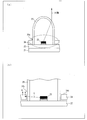
- FIG. 6A shows a cross-sectional configuration of one lens 25 portion of the illuminating device 12, and FIG. 6B further shows an enlarged portion surrounded by a broken line in FIG.
- a metal having a high reflectance is used as the material of the lens fixing plate 24. Therefore, the surface of the lens fixing plate 24 functions as a reflecting plate, and as shown in FIG. 6B, the light emitted from the LED chip 23 in the lateral direction (direction along the light irradiation surface of the illumination device 12) is The light is reflected at the side surface 24b of the hole 24a formed in the lens fixing plate 24 (see arrow B in FIG. 6B). Thereby, the light leak of the LED chip 23 to the said horizontal direction can be reduced, and the light from an LED chip can be irradiated to a plant more efficiently.
- a reflection sheet having a higher reflectance may be attached to the side surface 24b of the hole 24a formed in the lens fixing plate 24 (that is, the contact surface 24b with the lens 25). it can.
- the light leakage of the LED chip 23 in the lateral direction can be reduced, the light emission from each LED chip 23 becomes independent. Therefore, if a lighting method that partially controls the amount of light emission, such as local dimming that is used in backlights of liquid crystal display devices, is applied to the lighting device of the present invention, different characteristics (light quantity, wavelength) Etc.) can be selectively irradiated.
- the cooling plate 21 is abbreviate
- the lens fixing plate 24 and the LED substrate 22 are arranged very close to each other (substantially in contact), but in the structure shown in FIG. 7, the lens fixing plate 24 and the LED substrate are arranged. 22 are arranged at a predetermined distance from each other.
- FIG. 7A is an example of a configuration in which one lens 25a is provided for one LED chip 23.
- the lens 25a shown in this figure has a peripheral diameter of its bottom surface portion (contact portion with the LED substrate 22) larger than other portions.
- each LED chip 23 on the LED substrate 22 is covered with the lens 25a, and then the lens fixing plate 24 is covered, and the lens 25a is fixed by pressing the bottom surface of each lens 25a.
- FIG. 7B is a single member in which a plurality of lens protrusions 26 are connected. Also in this configuration, substantially like FIG. 7A, after placing each LED chip 23 on the LED substrate 22 so as to cover each protrusion 26 of the lens 25b, the lens fixing plate 24 is covered, The lens 25b is fixed by pressing the connecting portion between the protrusions 26.
- the peripheral diameter of the bottom surface portion (portion inserted into the hole 24a) is smaller than other portions.
- the lens 25c is individually fixed by inserting the bottom surface portion of the lens 25c into the hole 24a of the lens fixing plate 24.
- the lens 25d shown in (d) of FIG. 7 is a single member formed by connecting a plurality of lens protrusions 26, similarly to the lens 25b shown in (b) of FIG.
- this lens 25d as shown in FIG. 7D, after the lens fixing plate 24 is placed on the LED substrate 22, the bottom surface portion of each protrusion 26 of the lens 25d is fitted into each hole 24a. Then, screws 27 are inserted so as to penetrate the lens 25 d and the lens fixing plate 24, and the lens 25 d is fixed to the LED substrate 22.
- the lens 25 can be exchanged with respect to the LED substrate 22, and can be changed to a lens 25 having a different shape depending on the use of the plant cultivation apparatus 10.
- one lens (optical member) formed by connecting a plurality of lens protrusions 26 is provided on the entire surface of one LED substrate 22.
- the structure which is provided may be sufficient and one LED board 22 may be provided with two or more structures. In a configuration in which one lens is provided for one LED substrate 22, the lenses on the entire substrate can be exchanged at one time.
- the lens fixing plate is also divided according to each lens.
- the light irradiation surface of the illuminating device can be divided into a plurality of regions to which different lenses are attached, and the lenses can be individually exchanged for each region.
- FIG. 8A and 8B show an example in which the lens 25 is exchanged according to the growth of the plant 31.
- FIG. FIG. 8A shows an example of the illumination device 12 when the plant 31 is just germinated in the plant cultivation device 10.
- FIG.8 (b) an example of the illuminating device 12 after the plant 31 shown to (a) of FIG. 8 grew is shown.
- the cooling plate 21 is omitted.
- the lens 25e has a deeper bottom than the lens 25f.
- the light L1 from the LED light source irradiated through the deep lens 25e has a relatively narrow irradiation range and a relatively high light intensity. That is, light with high intensity is emitted toward the direction directly below the LED chip 23. Thereby, light can be efficiently irradiated to the small plant 31 that has just germinated.
- the lens 25f attached to the illumination device 12 after the plant has grown has a shallower shape than the lens 25e.
- the light L2 from the LED light source irradiated through the shallow lens 25f at the bottom is irradiated over a wider range than the light L2. Thereby, it is possible to irradiate light uniformly to the plant 31 that has grown greatly.
- the shape of the lens 25 can be changed according to the growth state of the plant.
- the light environment more suitable for the growth degree of the plant 31 can be created.
- the lens 25e is used when cultivating the plant 31 that has just germinated, although it is preferable to use the lens 25f at the time of cultivation of the plant 31 after growing, the present invention is not limited to this. That is, the lens used in the plant cultivation apparatus of the present invention may be selected from lenses that can create an optimal light environment according to the type and growth state of the plant.
- the structure that one lens 25g is provided with respect to several LED chip 23 is also possible.
- a lens 25g is used, for example, as shown in FIG. 8C, the irradiation light L3 from the three LED chips 23 can be condensed near the center thereof. Therefore, it is possible to concentrate and irradiate light on the place where the plant 31 is growing.
- the lens fixing plate 24 also needs to be replaced according to the shape of the lens.
- lens fixing plate 24 provided in the illumination device 12 described above is formed of a metal material
- the present invention is not limited to this.
- the material of the lens fixing plate for example, the same material as that of the light guide plate used for the backlight of the liquid crystal display panel can be used.
- FIG. 9A shows a cross-sectional configuration of one lens 25 portion of the illuminating device 12 when the lens fixing plate 34 is formed of a light guide plate, and FIG. The portion surrounded by the broken line is further enlarged and shown.
- the material for the lens fixing plate 34 in this case include transparent resins such as (meth) acrylic resin, COP (cycloolefin polymer), COC (cycloolefin copolymer), and polycarbonate. These transparent resins are the same as the materials suitable for the lens 25 described above. However, the present invention is not limited to this, and any material that can transmit light while propagating may be used.
- the light guide plate When the light guide plate is used as the material of the lens fixing plate 34 as described above, the light is emitted from the LED chip 23 in the lateral direction (the direction along the light irradiation surface of the illumination device 12) as shown in FIG.
- the emitted light propagates through the lens fixing plate 34 (see arrow C in FIG. 9B) and is emitted from the surface 34b (light irradiation surface) of the lens fixing plate 34 (see FIG. 9B).
- Arrow D Thereby, since light can be emitted also from a region where the LED chip 23 is not arranged, unevenness in light and darkness of the entire illumination device 12 can be reduced. Moreover, even if the number of LED chips 23 is reduced, relatively uniform light can be irradiated, so that the cost can be reduced.
- the LED chip 23 is covered with the lens 25 and the lens fixing plate 34, and thus is in contact with the space in which the plant 31 is disposed. Absent. Therefore, as in the case where the lens fixing plate is made of metal, the LED chip 23 is not damaged by condensation, and the reliability of the LED chip 23 can be improved and the life of the LED chip 23 can be increased. Can be extended. However, since the light guide plate has a lower thermal conductivity than a metal, the cooling effect is less than that of the lens fixing plate 24 formed of a metal material.
- the material for the lens fixing plate may be a high thermal conductive resin.
- the high thermal conductive resin a commercially available “high thermal conductive resin” can be used.
- Specific examples of the high thermal conductive resin include high thermal conductive PPS (polyphenylene sulfide resin).
- a sheet obtained by blending and designing a polymer such as acrylic or silicon and a heat conductive filler can be used as a lens fixing plate made of a high heat conductive resin.
- the lens fixing plate 24 absorbs heat generated from the LED chip and can efficiently dissipate heat. Therefore, the cooling effect of the LED chip can be enhanced.
- the LED chip in the horizontal direction can be obtained by attaching a reflective sheet having a higher reflectance to the side surface of the hole 34a formed in the lens fixing plate 34 (that is, the contact surface with the lens 25). 23 light leakage can be reduced, and the light from the LED chip can be irradiated to the plant more efficiently.
- the reflection sheet may be provided on a surface of the lens fixing plate 34 opposite to the light irradiation surface 34b. Thereby, light can be more efficiently emitted to the light irradiation surface 34b side.
- a configuration in which a reflection portion having a predetermined shape (for example, dot shape) is partially printed on the surface can be employed. .
- the external appearance of the plant cultivation apparatus 10 according to the present embodiment is as shown in FIG.
- the plant cultivation apparatus 10 is provided with the illumination device 42 according to the present embodiment.
- FIG. 10 the perspective view of the illuminating device 42 is shown.
- the illuminating device 42 is shown in a state that is upside down from the state provided in the plant cultivation device 10.
- FIG. 11 each structural member which comprises the illuminating device 42 is decomposed
- FIG. 12A one lens portion of the illumination device 42 is shown enlarged.
- the LED substrate 52 (substrate), the heat conductive sheet 56, and the lens fixing plate 54 (fixing plate, optical member) are arranged in this order on the cooling plate 51. It is piled up.
- the cooling plate 51 is provided on the back side of the LED substrate 52 and can absorb the heat generated from the LED chip 53 during light irradiation.
- the LED substrate 52 has a configuration in which a plurality of LED chips 53 (LED packages) are arranged on a substrate 52a (for example, an insulating substrate).
- the LED chip 53 (light emitting diode) can adopt the same configuration as the LED chip 23 of the first embodiment.
- each LED chip may emit light in the same color, or may be composed of a plurality of types of LED chips that emit light of different wavelengths.
- the lens fixing plate 54 has holes 54 a formed in accordance with the LED chips 53 arranged on the LED substrate 52. Accordingly, as shown in FIG. 12A, when the lens fixing plate 54 and the LED substrate 52 are overlapped, the LED chips 53 are arranged in the portions of the holes 54a.
- the lens fixing plate 54 is formed of a resin having a light guide property (light propagation property). That is, like the lens fixing plate 34 shown in FIG. 9, it is formed of a light guide plate. More specifically, the lens fixing plate 54 can be formed of a transparent resin such as (meth) acrylic resin, COP (cycloolefin polymer), COC (cycloolefin copolymer), or polycarbonate.
- a heat conductive sheet 56 is provided between the LED substrate 52 and the lens fixing plate 54 in addition to the above-described plates.
- holes 56 a are formed in the heat conductive sheet 56 according to the LED chips 53 arranged on the LED substrate 52.
- each LED chip 53 will be arrange
- the material of the heat conductive sheet 56 include a heat conductive olefin compound. Specific examples include thermal conductive sheets manufactured by Furukawa Electric Co., Ltd. or Electrochemical Industry Co., Ltd., but are not limited thereto.
- FIG. 12B shows the planar configuration of a part of the lens fixing plate 54 and the heat conductive sheet 56, respectively, and the cross-sectional configuration of the XX ′ line portion shown in FIG. This is shown in FIG.
- the lens 55 in each hole 54a and 56a formed in the lens fixing plate 54 and the heat conductive sheet 56, the lens 55 (in order to adjust the optical path of the irradiation light from LED) An optical path changing unit and an optical member) are fitted. That is, the lens 55 is disposed on the LED substrate 52 through the lens fixing plate 54 and the heat conductive sheet 56. The lens 55 is for adjusting the intensity distribution in each direction of the light emitted from the LED chip 53 (that is, the light distribution of the LED).
- the light distribution of this LED can be adjusted by appropriately changing the shape of the lens 55 in accordance with Snell's law. Specifically, the curvature of the curved surface of the projection of the lens 55 having a convex shape is changed, and the optical path of light emitted from the LED chip 53 is changed to an LED as indicated by an arrow A in FIG.
- the substrate 52 can be bent in a direction perpendicular to the light exit surface.
- the same material as the lens 25 of the first embodiment can be applied.
- FIG. 12 is a cross-sectional view showing a part of the illumination device shown in (a) of FIG. Note that a part of the lighting device illustrated in FIG. 12C is a portion surrounded by a broken line in FIG. This portion corresponds to the cross section of the X-X ′ line portion in the lens fixing plate 54 and the heat conductive sheet 56 shown in FIG.
- the illumination device 42 of the present embodiment is provided with a lens fixing plate 54 formed of a material having light propagation performance on the outermost surface of a laminated structure composed of a plurality of plates. It has been. Therefore, the light emitted from the LED chip 53 in the lateral direction (the direction along the light irradiation surface of the illumination device 42) propagates through the lens fixing plate 54 (see arrow B in FIG. 12C), and the lens. The light is emitted from the surface 54b of the fixed plate 54 (arrow C in FIG. 12C). Thereby, since light can be emitted also from the region where the LED chip 53 is not disposed, the brightness unevenness of the entire illumination device 42 can be reduced. Further, even if the number of LED chips 53 is reduced, relatively uniform light can be irradiated, so that the cost can be reduced.
- the heat conductive sheet 56 formed of a material having high heat conductivity includes the LED substrate 52 and the light. It arrange
- the lens 55 and the lens fixing plate 54 are separate constituent members, and each lens 55 is attached to and detached from a hole 54a formed in the lens fixing plate 54. It is configured to be fitted in a possible state. Thereby, it becomes possible to replace
- a lens fixing plate 54 and a lens 55 are provided between the LED chip 53 and the plant 31.
- the LED chip 53 is covered with the lens 55 and the lens fixing plate 54, and is not contacting the space where the plant 31 is arrange
- an illumination device that irradiates light to a plant, and includes a light-emitting diode as a light source, a substrate on which the light-emitting diodes are arranged, and the substrate. And an optical member that changes the optical path of the irradiation light from the light-emitting diode, and the optical member is attached to the apparatus in a state where it can be attached and detached. It is characterized by being.
- an optical member that can change the optical path of light from the light emitting diode is attached to the device in a detachable state.
- “changing the optical path” means changing the irradiation range and irradiation direction of light from the state emitted from the light source.
- the expression “changing the light path of the light emitting diode” can be rephrased as “adjusting the light distribution of the light emitting diode”.
- the irradiation range and irradiation direction of the light irradiated from the light emitting diode can be changed by replacing optical members having different characteristics according to the purpose. Therefore, according to the illuminating device of the present invention, it is possible to perform efficient light irradiation according to the type of plant to be irradiated and the growth state.
- an optical member is provided between the plant and the substrate on which the light emitting diodes are arranged.
- it can be set as the structure where the heat which generate
- the optical member absorbs heat generated from the surface of the light emitting diode and the substrate, and can be efficiently radiated. Therefore, the cooling effect of the light emitting diode can be further enhanced as compared with the conventional configuration in which only the cooling plate is provided on the back surface of the substrate.
- the optical member is provided between the plant and the light emitting diode installation substrate, the area in contact with the outside air on the substrate on which the light emitting diode is mounted is reduced. For this reason, even if a temperature difference occurs between the space where the plant is placed and the light emitting diode, and the condensation occurs, the substrate is less likely to be cooled by the outside air and the light emitting diode is less likely to cause the condensation. it can. Therefore, the light emitting diode is not damaged by condensation, and the reliability of the light emitting diode can be improved and the life of the light emitting diode can be extended.
- the optical member includes an optical path changing unit and a fixing plate for fixing the optical path changing unit, and the fixing plate is disposed on the substrate. And the optical path changing portion may be attached to the hole.
- the optical path changing unit it is possible to change only the optical path changing unit to a different type with the fixed plate attached to the apparatus. Therefore, it is possible to easily adjust the irradiation light from the light emitting diode to a desired light distribution state according to the growth state of the plant, the kind of the plant, and the like.
- the light-emitting diode provided on the substrate is cut off from the space where the plant is arranged by fitting the optical path changing unit such as a lens into the hole formed in the fixed plate. Will be. For this reason, even if condensation occurs due to a temperature difference between the space where the plant is placed and the light emitting diode, the surface of the fixed plate and the optical path changing unit (the boundary with the space where the plant is placed) In the light emitting diode, no condensation occurs. Therefore, the light emitting diode is not damaged by condensation, and the reliability of the light emitting diode can be improved and the life of the light emitting diode can be extended.
- one or a plurality of light emitting diodes may be used as one unit, and one optical path changing unit may be provided for each unit.
- the optical path changing unit can be changed for each unit composed of one or a plurality of light emitting diodes. Therefore, the optical path of the irradiation light from a light emitting diode can be varied according to the position where the light emitting diode is provided. Within the same lighting device, the characteristics of irradiation light (irradiation range, irradiation direction, etc.) can be adjusted for each region in accordance with the state of the plant to be irradiated.
- the optical member is composed of a plurality of members, and may be attached to the device in a state in which attachment and removal are possible for each constituent member.
- the light irradiation surface of the lighting device can be divided into a plurality of regions to which different components are attached, and the optical member can be individually replaced for each region.
- the fixing plate may be formed of a metal material.
- the fixing plate provided between the plant and the substrate on which the light emitting diode is installed is formed of the metal material having high thermal conductivity, so that the heat generated from the light emitting diode is heated.
- the conductive sheet absorbs and can efficiently dissipate heat. Therefore, the cooling effect of the light emitting diode can be further enhanced.
- the fixing plate may be formed of a resin having a light guide property.
- the light emitted from the light emitting diode can be efficiently emitted to the side on which the plant is placed while propagating through the resin having a light guide property.
- light having a relatively high intensity can be emitted from a region on the substrate where the light emitting diodes are not arranged. Therefore, even when the number of light emitting diodes is reduced, light having a uniform or wide irradiation range can be obtained.
- An illumination device that can irradiate can be realized.
- the fixing plate may have a configuration in which a reflective sheet is further attached to the light-guiding resin.
- the light emitted from the light emitting diode is propagated through the resin having light guide property, and the light is efficiently emitted to the side on which the plant is placed by the reflection action of the reflection sheet. Can be made. Thereby, even when the number of light emitting diodes is reduced, it is possible to realize an illumination device that can irradiate light with a uniform or wide irradiation range.
- a heat conductive sheet may be further provided between the substrate and the fixed plate.
- the heat conductive sheet absorbs the heat generated from the light emitting diode, and can be efficiently dissipated. Therefore, the cooling effect of the light emitting diode can be further enhanced.
- the fixing plate may be formed of a high thermal conductive resin.
- the fixing plate formed of the high thermal conductive resin emitted from the light emitting diode can absorb and efficiently dissipate heat. Therefore, the cooling effect of the light emitting diode can be further enhanced.
- the optical path changing unit may be a lens.
- the characteristics (irradiation range, irradiation direction, etc.) of light irradiated from the light emitting diode can be easily changed by using lenses having different shapes.
- a cooling plate may be further provided on the back surface of the substrate.
- the plant cultivation apparatus according to the present invention includes any one of the above-described lighting apparatuses.
- the plant cultivation apparatus of the present invention can change the irradiation range and irradiation direction of the light emitted from the light emitting diode according to the purpose. Moreover, in the plant cultivation apparatus of this invention, it can be set as the structure where the heat
- the optical member is provided between the plant and the light emitting diode installation substrate, so that a temperature difference occurs between the space where the plant is disposed and the light emitting diode, thereby causing dew condensation. Even when this occurs, the light-emitting diode can have a structure in which condensation does not easily occur. Therefore, the light emitting diode is not damaged by condensation, and the reliability of the light emitting diode can be improved and the life of the light emitting diode can be extended.
- the present invention can be applied to an artificial light source of a plant factory or a plant cultivation apparatus for cultivating plants such as vegetables indoors.
- Cooling plate 22 LED board (board
Landscapes
- Life Sciences & Earth Sciences (AREA)
- Engineering & Computer Science (AREA)
- General Engineering & Computer Science (AREA)
- Environmental Sciences (AREA)
- Biodiversity & Conservation Biology (AREA)
- Botany (AREA)
- Ecology (AREA)
- Forests & Forestry (AREA)
- Cultivation Of Plants (AREA)
- Planar Illumination Modules (AREA)
Abstract
L'invention porte sur un appareil d'éclairage (12) pour rayonner de la lumière sur des plantes. L'appareil d'éclairage (12) comporte des diodes électroluminescentes (23) constituant des sources de lumière ; un substrat de diodes électroluminescentes (22) qui comporte les diodes électroluminescentes (23) disposées sur celui-ci, côte-à-côte ; des lentilles (25) (élément optique) qui sont formées entre le substrat de diodes électroluminescentes (22) et la plante devant être soumise à un rayonnement, et qui changent les trajets de lumière rayonnée par les diodes électroluminescentes (23) ; et une plaque de support de lentilles (24) (élément optique) pour supporter les lentilles (25) en place. Les lentilles (25) sont montées sur l'appareil dans un état pouvant être fixées/pouvant être détachées. Par conséquent, il est procuré un appareil d'éclairage pour la culture de plantes, dans lequel des améliorations ont été apportées du point de vue de la commande de génération de chaleur et du réglage de distribution de lumière des diodes électroluminescentes.
Priority Applications (1)
| Application Number | Priority Date | Filing Date | Title |
|---|---|---|---|
| US13/637,906 US20130021797A1 (en) | 2010-03-31 | 2010-11-29 | Illumination apparatus and plant cultivation apparatus |
Applications Claiming Priority (2)
| Application Number | Priority Date | Filing Date | Title |
|---|---|---|---|
| JP2010-083350 | 2010-03-31 | ||
| JP2010083350 | 2010-03-31 |
Publications (1)
| Publication Number | Publication Date |
|---|---|
| WO2011121845A1 true WO2011121845A1 (fr) | 2011-10-06 |
Family
ID=44711618
Family Applications (1)
| Application Number | Title | Priority Date | Filing Date |
|---|---|---|---|
| PCT/JP2010/071276 Ceased WO2011121845A1 (fr) | 2010-03-31 | 2010-11-29 | Appareil d'éclairage et appareil de culture de plantes |
Country Status (2)
| Country | Link |
|---|---|
| US (1) | US20130021797A1 (fr) |
| WO (1) | WO2011121845A1 (fr) |
Cited By (3)
| Publication number | Priority date | Publication date | Assignee | Title |
|---|---|---|---|---|
| JP2013158317A (ja) * | 2012-02-07 | 2013-08-19 | Kyoto Univ | 完全制御型植物工場における植物栽培装置及び植物栽培方法 |
| BE1020512A3 (fr) * | 2012-03-02 | 2013-12-03 | Colasse S A | Systeme d'eclairage led. |
| JP2019193616A (ja) * | 2018-04-30 | 2019-11-07 | モンディ・プロダクツ・リミテッドMondi Products Ltd. | 光を用いた植物栽培器 |
Families Citing this family (27)
| Publication number | Priority date | Publication date | Assignee | Title |
|---|---|---|---|---|
| US8666247B2 (en) * | 2010-08-25 | 2014-03-04 | Ciena Corporation | Bandwidth defragmentation systems and methods in optical networks |
| US8714774B2 (en) * | 2011-09-08 | 2014-05-06 | GE Lighting Solutions, LLC | Light emitting diode (LED) light fixture for a greenhouse and a greenhouse incorporating a LED light fixture |
| JP6032775B2 (ja) * | 2012-07-11 | 2016-11-30 | フィリップス ライティング ホールディング ビー ヴィ | 植物育成光を提供可能な照明装置及び植物育成照明方法 |
| US9976710B2 (en) | 2013-10-30 | 2018-05-22 | Lilibrand Llc | Flexible strip lighting apparatus and methods |
| JP5732157B1 (ja) * | 2014-03-07 | 2015-06-10 | 株式会社環境フォトニクス | 光照射装置 |
| US20170080117A1 (en) * | 2014-07-16 | 2017-03-23 | LiteProducts LLC | System and method for inactivating pathogens using visible light and/or uv light |
| EP3175170B8 (fr) * | 2014-07-30 | 2018-07-04 | Philips Lighting Holding B.V. | Procédés et appareil de conception de support de système optique |
| US20160157439A1 (en) * | 2014-12-09 | 2016-06-09 | The Plastics Group, Inc. | Plant and garden growing system |
| TW201625128A (zh) * | 2015-01-05 | 2016-07-16 | 金寶生物科技股份有限公司 | 植物光照設備 |
| USD767806S1 (en) | 2015-05-27 | 2016-09-27 | Marcelo L. Colacilli | LED cinema light |
| US20200232623A1 (en) * | 2015-09-29 | 2020-07-23 | Osram Sylvania Inc. | Formed cellular lighting elements and lighting devices including the same |
| DE102016103370A1 (de) * | 2016-02-25 | 2017-08-31 | Trilux Gmbh & Co. Kg | Invertierte LED-Leiterkarte |
| US10132476B2 (en) | 2016-03-08 | 2018-11-20 | Lilibrand Llc | Lighting system with lens assembly |
| WO2018039920A1 (fr) * | 2016-08-30 | 2018-03-08 | 广东森维绿联科技有限公司 | Structure de matrice de led interactive pour dispositif de plantation intelligent |
| US12388056B1 (en) | 2017-01-27 | 2025-08-12 | Korrus, Inc. | Linear lighting systems and processes |
| CN110998880A (zh) | 2017-01-27 | 2020-04-10 | 莉莉布兰德有限责任公司 | 具有高显色指数和均匀平面照明的照明系统 |
| US20180328552A1 (en) | 2017-03-09 | 2018-11-15 | Lilibrand Llc | Fixtures and lighting accessories for lighting devices |
| US10314243B2 (en) * | 2017-09-21 | 2019-06-11 | Osram Sylvania Inc. | Horticultural light module assembly |
| US10749395B2 (en) | 2018-04-19 | 2020-08-18 | Siemens Energy, Inc. | Assembly and method for preventing axial migration of springs in generator rotors |
| US11041609B2 (en) * | 2018-05-01 | 2021-06-22 | Ecosense Lighting Inc. | Lighting systems and devices with central silicone module |
| IT201800010622A1 (it) * | 2018-11-27 | 2020-05-27 | Lux Ledlighting S R L | Dispositivo di illuminazione a led per una superficie coltivata |
| CN114364913B (zh) | 2018-12-17 | 2025-10-28 | 克鲁斯有限公司 | 符合ac驱动功率的条带照明系统 |
| JP2022519745A (ja) * | 2019-02-08 | 2022-03-24 | ダブリュ.エル.ゴア アンド アソシエイツ,インコーポレイティド | 農業環境のための光拡散反射性カーテン |
| CA3150287A1 (fr) * | 2019-08-20 | 2021-02-25 | GrowOp World Ltd. | Systeme compact pour espace ferme pour l'eclairage, le conditionnement d'air et la purification de l'air |
| FR3121308B1 (fr) | 2021-03-23 | 2023-12-22 | Appleton Grp Llc | Moteur de lumière à LED classé ZONE IEC 1 utilisant une optique pré-moulée |
| KR102789319B1 (ko) * | 2022-03-22 | 2025-04-03 | (주)이그린글로벌 | 감자 조직배양용 배양장치 |
| FR3135511B1 (fr) * | 2022-05-16 | 2024-07-19 | Appleton Grp Llc | Moteur de lumière à DEL certifié IEC ZONE utilisant une couche d’encapsulation pré-moulée et une feuille de métal |
Citations (3)
| Publication number | Priority date | Publication date | Assignee | Title |
|---|---|---|---|---|
| JP2005318821A (ja) * | 2004-05-07 | 2005-11-17 | Palcom Corp | 照光装置 |
| JP2006331817A (ja) * | 2005-05-25 | 2006-12-07 | Matsushita Electric Works Ltd | 発光装置及びそれを用いた照明器具 |
| JP2007115424A (ja) * | 2005-10-18 | 2007-05-10 | Enplas Corp | 照明装置及び照明ユニット |
Family Cites Families (2)
| Publication number | Priority date | Publication date | Assignee | Title |
|---|---|---|---|---|
| US5632551A (en) * | 1994-07-18 | 1997-05-27 | Grote Industries, Inc. | LED vehicle lamp assembly |
| US6819303B1 (en) * | 1998-08-17 | 2004-11-16 | Daktronics, Inc. | Control system for an electronic sign (video display system) |
-
2010
- 2010-11-29 US US13/637,906 patent/US20130021797A1/en not_active Abandoned
- 2010-11-29 WO PCT/JP2010/071276 patent/WO2011121845A1/fr not_active Ceased
Patent Citations (3)
| Publication number | Priority date | Publication date | Assignee | Title |
|---|---|---|---|---|
| JP2005318821A (ja) * | 2004-05-07 | 2005-11-17 | Palcom Corp | 照光装置 |
| JP2006331817A (ja) * | 2005-05-25 | 2006-12-07 | Matsushita Electric Works Ltd | 発光装置及びそれを用いた照明器具 |
| JP2007115424A (ja) * | 2005-10-18 | 2007-05-10 | Enplas Corp | 照明装置及び照明ユニット |
Cited By (5)
| Publication number | Priority date | Publication date | Assignee | Title |
|---|---|---|---|---|
| JP2013158317A (ja) * | 2012-02-07 | 2013-08-19 | Kyoto Univ | 完全制御型植物工場における植物栽培装置及び植物栽培方法 |
| BE1020512A3 (fr) * | 2012-03-02 | 2013-12-03 | Colasse S A | Systeme d'eclairage led. |
| JP2019193616A (ja) * | 2018-04-30 | 2019-11-07 | モンディ・プロダクツ・リミテッドMondi Products Ltd. | 光を用いた植物栽培器 |
| US11166417B2 (en) | 2018-04-30 | 2021-11-09 | Mondi Products Ltd. | Plant cultivator with light |
| US11910766B2 (en) | 2018-04-30 | 2024-02-27 | Mondi Products Ltd. | Plant cultivator with light |
Also Published As
| Publication number | Publication date |
|---|---|
| US20130021797A1 (en) | 2013-01-24 |
Similar Documents
| Publication | Publication Date | Title |
|---|---|---|
| WO2011121845A1 (fr) | Appareil d'éclairage et appareil de culture de plantes | |
| US20100002444A1 (en) | Bulb-shaped led lamp and compact led lamp | |
| US20120127756A1 (en) | Lighting module | |
| JP2006286638A (ja) | 複数の隣り合って重なり合う導光板を有する発光装置 | |
| JP2006286639A (ja) | 光を放射するための凹部を形成する複数の重なり合うパネルを有する発光装置 | |
| CN101135810A (zh) | 背光单元以及使用其的液晶显示设备 | |
| JP2011014535A (ja) | 照明装置 | |
| US9395063B2 (en) | LED lighting engine adopting an icicle type diffusion unit | |
| TW201105898A (en) | Luminous module and lighting apparatus | |
| CN103165590B (zh) | 发光二极管与直下式背光源 | |
| WO2012063917A1 (fr) | Dispositif d'éclairage et dispositif d'affichage à cristaux liquides le comprenant | |
| US11125931B2 (en) | Display apparatus | |
| US8511885B2 (en) | Light emitting device assembly, backlight unit and display device having the same | |
| JP5133439B2 (ja) | 照明装置、及びそれを備えた照明機器 | |
| WO2012144393A1 (fr) | Dispositif d'éclairage et appareil d'éclairage le comportant | |
| WO2012144310A1 (fr) | Dispositif de source de lumière et dispositif électronique le comportant | |
| KR20120009558A (ko) | 백라이트 유닛 및 이를 포함하는 표시장치 | |
| US20130215600A1 (en) | Light source package and backlight unit including the light source package | |
| WO2012035898A1 (fr) | Dispositif d'éclairage et dispositif d'affichage à cristaux liquides pourvu de celui-ci | |
| KR101700791B1 (ko) | 표시장치 | |
| JP2012226965A (ja) | 照明装置、及びそれを備えた照明機器 | |
| CN101725901A (zh) | 光源模组 | |
| TW200847460A (en) | A structure of LED lighting device | |
| KR20060128551A (ko) | 직하형 백라이트 유닛 | |
| JP2012226967A (ja) | 照明装置、及びそれを備えた照明機器 |
Legal Events
| Date | Code | Title | Description |
|---|---|---|---|
| 121 | Ep: the epo has been informed by wipo that ep was designated in this application |
Ref document number: 10849016 Country of ref document: EP Kind code of ref document: A1 |
|
| WWE | Wipo information: entry into national phase |
Ref document number: 13637906 Country of ref document: US |
|
| NENP | Non-entry into the national phase |
Ref country code: DE |
|
| 122 | Ep: pct application non-entry in european phase |
Ref document number: 10849016 Country of ref document: EP Kind code of ref document: A1 |
|
| NENP | Non-entry into the national phase |
Ref country code: JP |