WO2011122190A1 - Substrat de module d'élément électroluminescent, module d'élément électroluminescent et dispositif d'éclairage - Google Patents
Substrat de module d'élément électroluminescent, module d'élément électroluminescent et dispositif d'éclairage Download PDFInfo
- Publication number
- WO2011122190A1 WO2011122190A1 PCT/JP2011/054321 JP2011054321W WO2011122190A1 WO 2011122190 A1 WO2011122190 A1 WO 2011122190A1 JP 2011054321 W JP2011054321 W JP 2011054321W WO 2011122190 A1 WO2011122190 A1 WO 2011122190A1
- Authority
- WO
- WIPO (PCT)
- Prior art keywords
- light emitting
- emitting element
- layer
- element module
- module substrate
- Prior art date
- Legal status (The legal status is an assumption and is not a legal conclusion. Google has not performed a legal analysis and makes no representation as to the accuracy of the status listed.)
- Ceased
Links
Images






Classifications
-
- H—ELECTRICITY
- H10—SEMICONDUCTOR DEVICES; ELECTRIC SOLID-STATE DEVICES NOT OTHERWISE PROVIDED FOR
- H10H—INORGANIC LIGHT-EMITTING SEMICONDUCTOR DEVICES HAVING POTENTIAL BARRIERS
- H10H20/00—Individual inorganic light-emitting semiconductor devices having potential barriers, e.g. light-emitting diodes [LED]
- H10H20/80—Constructional details
- H10H20/83—Electrodes
- H10H20/832—Electrodes characterised by their material
- H10H20/835—Reflective materials
-
- H—ELECTRICITY
- H05—ELECTRIC TECHNIQUES NOT OTHERWISE PROVIDED FOR
- H05K—PRINTED CIRCUITS; CASINGS OR CONSTRUCTIONAL DETAILS OF ELECTRIC APPARATUS; MANUFACTURE OF ASSEMBLAGES OF ELECTRICAL COMPONENTS
- H05K3/00—Apparatus or processes for manufacturing printed circuits
- H05K3/22—Secondary treatment of printed circuits
- H05K3/24—Reinforcing of the conductive pattern
- H05K3/241—Reinforcing of the conductive pattern characterised by the electroplating method; means therefor, e.g. baths or apparatus
- H05K3/242—Reinforcing of the conductive pattern characterised by the electroplating method; means therefor, e.g. baths or apparatus characterised by using temporary conductors on the printed circuit for electrically connecting areas which are to be electroplated
-
- H—ELECTRICITY
- H10—SEMICONDUCTOR DEVICES; ELECTRIC SOLID-STATE DEVICES NOT OTHERWISE PROVIDED FOR
- H10H—INORGANIC LIGHT-EMITTING SEMICONDUCTOR DEVICES HAVING POTENTIAL BARRIERS
- H10H20/00—Individual inorganic light-emitting semiconductor devices having potential barriers, e.g. light-emitting diodes [LED]
- H10H20/80—Constructional details
- H10H20/85—Packages
- H10H20/857—Interconnections, e.g. lead-frames, bond wires or solder balls
-
- H—ELECTRICITY
- H10—SEMICONDUCTOR DEVICES; ELECTRIC SOLID-STATE DEVICES NOT OTHERWISE PROVIDED FOR
- H10W—GENERIC PACKAGES, INTERCONNECTIONS, CONNECTORS OR OTHER CONSTRUCTIONAL DETAILS OF DEVICES COVERED BY CLASS H10
- H10W90/00—Package configurations
-
- F—MECHANICAL ENGINEERING; LIGHTING; HEATING; WEAPONS; BLASTING
- F21—LIGHTING
- F21K—NON-ELECTRIC LIGHT SOURCES USING LUMINESCENCE; LIGHT SOURCES USING ELECTROCHEMILUMINESCENCE; LIGHT SOURCES USING CHARGES OF COMBUSTIBLE MATERIAL; LIGHT SOURCES USING SEMICONDUCTOR DEVICES AS LIGHT-GENERATING ELEMENTS; LIGHT SOURCES NOT OTHERWISE PROVIDED FOR
- F21K9/00—Light sources using semiconductor devices as light-generating elements, e.g. using light-emitting diodes [LED] or lasers
- F21K9/20—Light sources comprising attachment means
- F21K9/23—Retrofit light sources for lighting devices with a single fitting for each light source, e.g. for substitution of incandescent lamps with bayonet or threaded fittings
- F21K9/232—Retrofit light sources for lighting devices with a single fitting for each light source, e.g. for substitution of incandescent lamps with bayonet or threaded fittings specially adapted for generating an essentially omnidirectional light distribution, e.g. with a glass bulb
-
- F—MECHANICAL ENGINEERING; LIGHTING; HEATING; WEAPONS; BLASTING
- F21—LIGHTING
- F21Y—INDEXING SCHEME ASSOCIATED WITH SUBCLASSES F21K, F21L, F21S and F21V, RELATING TO THE FORM OR THE KIND OF THE LIGHT SOURCES OR OF THE COLOUR OF THE LIGHT EMITTED
- F21Y2115/00—Light-generating elements of semiconductor light sources
- F21Y2115/10—Light-emitting diodes [LED]
-
- H—ELECTRICITY
- H05—ELECTRIC TECHNIQUES NOT OTHERWISE PROVIDED FOR
- H05K—PRINTED CIRCUITS; CASINGS OR CONSTRUCTIONAL DETAILS OF ELECTRIC APPARATUS; MANUFACTURE OF ASSEMBLAGES OF ELECTRICAL COMPONENTS
- H05K1/00—Printed circuits
- H05K1/02—Details
- H05K1/03—Use of materials for the substrate
- H05K1/05—Insulated conductive substrates, e.g. insulated metal substrate
- H05K1/056—Insulated conductive substrates, e.g. insulated metal substrate the metal substrate being covered by an organic insulating layer
-
- H—ELECTRICITY
- H05—ELECTRIC TECHNIQUES NOT OTHERWISE PROVIDED FOR
- H05K—PRINTED CIRCUITS; CASINGS OR CONSTRUCTIONAL DETAILS OF ELECTRIC APPARATUS; MANUFACTURE OF ASSEMBLAGES OF ELECTRICAL COMPONENTS
- H05K2201/00—Indexing scheme relating to printed circuits covered by H05K1/00
- H05K2201/10—Details of components or other objects attached to or integrated in a printed circuit board
- H05K2201/10007—Types of components
- H05K2201/10106—Light emitting diode [LED]
-
- H—ELECTRICITY
- H05—ELECTRIC TECHNIQUES NOT OTHERWISE PROVIDED FOR
- H05K—PRINTED CIRCUITS; CASINGS OR CONSTRUCTIONAL DETAILS OF ELECTRIC APPARATUS; MANUFACTURE OF ASSEMBLAGES OF ELECTRICAL COMPONENTS
- H05K2201/00—Indexing scheme relating to printed circuits covered by H05K1/00
- H05K2201/20—Details of printed circuits not provided for in H05K2201/01 - H05K2201/10
- H05K2201/2054—Light-reflecting surface, e.g. conductors, substrates, coatings, dielectrics
-
- H—ELECTRICITY
- H05—ELECTRIC TECHNIQUES NOT OTHERWISE PROVIDED FOR
- H05K—PRINTED CIRCUITS; CASINGS OR CONSTRUCTIONAL DETAILS OF ELECTRIC APPARATUS; MANUFACTURE OF ASSEMBLAGES OF ELECTRICAL COMPONENTS
- H05K3/00—Apparatus or processes for manufacturing printed circuits
- H05K3/0097—Processing two or more printed circuits simultaneously, e.g. made from a common substrate, or temporarily stacked circuit boards
-
- H—ELECTRICITY
- H10—SEMICONDUCTOR DEVICES; ELECTRIC SOLID-STATE DEVICES NOT OTHERWISE PROVIDED FOR
- H10H—INORGANIC LIGHT-EMITTING SEMICONDUCTOR DEVICES HAVING POTENTIAL BARRIERS
- H10H20/00—Individual inorganic light-emitting semiconductor devices having potential barriers, e.g. light-emitting diodes [LED]
- H10H20/80—Constructional details
- H10H20/85—Packages
- H10H20/855—Optical field-shaping means, e.g. lenses
- H10H20/856—Reflecting means
-
- H—ELECTRICITY
- H10—SEMICONDUCTOR DEVICES; ELECTRIC SOLID-STATE DEVICES NOT OTHERWISE PROVIDED FOR
- H10W—GENERIC PACKAGES, INTERCONNECTIONS, CONNECTORS OR OTHER CONSTRUCTIONAL DETAILS OF DEVICES COVERED BY CLASS H10
- H10W72/00—Interconnections or connectors in packages
- H10W72/071—Connecting or disconnecting
- H10W72/075—Connecting or disconnecting of bond wires
- H10W72/07551—Connecting or disconnecting of bond wires characterised by changes in properties of the bond wires during the connecting
- H10W72/07554—Connecting or disconnecting of bond wires characterised by changes in properties of the bond wires during the connecting changes in dispositions
-
- H—ELECTRICITY
- H10—SEMICONDUCTOR DEVICES; ELECTRIC SOLID-STATE DEVICES NOT OTHERWISE PROVIDED FOR
- H10W—GENERIC PACKAGES, INTERCONNECTIONS, CONNECTORS OR OTHER CONSTRUCTIONAL DETAILS OF DEVICES COVERED BY CLASS H10
- H10W72/00—Interconnections or connectors in packages
- H10W72/50—Bond wires
- H10W72/541—Dispositions of bond wires
- H10W72/547—Dispositions of multiple bond wires
-
- H—ELECTRICITY
- H10—SEMICONDUCTOR DEVICES; ELECTRIC SOLID-STATE DEVICES NOT OTHERWISE PROVIDED FOR
- H10W—GENERIC PACKAGES, INTERCONNECTIONS, CONNECTORS OR OTHER CONSTRUCTIONAL DETAILS OF DEVICES COVERED BY CLASS H10
- H10W90/00—Package configurations
- H10W90/701—Package configurations characterised by the relative positions of pads or connectors relative to package parts
- H10W90/751—Package configurations characterised by the relative positions of pads or connectors relative to package parts of bond wires
- H10W90/753—Package configurations characterised by the relative positions of pads or connectors relative to package parts of bond wires between laterally-adjacent chips
Definitions
- the present invention relates to a light emitting element module substrate, a light emitting element module, and a lighting device.
- Patent Document 1 discloses a light emitting device including a substrate, a plurality of light emitting elements arranged on the substrate, and a phosphor layer.
- Luminescence efficiency of light emitting elements decreases at high temperatures.
- a laminated plate of a metal plate and an insulating layer provided thereon is used as a substrate.
- the thickness of the insulating layer is set to a certain value or less in order to increase the thermal conductivity between the LED element and the metal plate.
- a metal layer having a mounting portion on which the LED element is mounted and a bonding portion for electrical connection of the LED element is provided on the insulating layer of the laminate. This metal layer is required to have high bonding properties as well as high reflectivity.
- the insulating layer is thin, so that the insulating properties of the metal plate of the laminate plate and the metal layer deteriorate at the end portion of the substrate, The desired operation cannot be obtained.
- the mounting portion and the bonding portion using the metal layer are required to have high reflectivity and high bonding property, and at the same time, be electrically insulated from the end portion of the substrate.
- the present invention provides a light-emitting element module substrate, a light-emitting element module, and a lighting device having a mounting portion and a bonding portion that have high reflectivity, high bonding properties, and excellent electrical insulation with an end portion.
- a light emitting element module substrate provided with a laminate and a metal layer.
- the laminated plate includes a base metal plate and an insulating layer provided on the base metal plate.
- the metal layer is provided on the insulating layer.
- the metal layer includes a mounting portion on which a light emitting element is mounted and a bonding portion to which a wiring electrically connected to the light emitting element is bonded.
- the metal layer is a top layer of at least one of the mounting part and the bonding part, and includes a silver layer formed by electrolytic plating. The mounting portion and the bonding portion are electrically cut off from the peripheral edge of the laminated plate.
- a light emitting element module substrate provided with a laminate and a metal layer.
- the laminated plate includes a base metal plate and an insulating layer provided on the base metal plate.
- the metal layer is provided on the insulating layer.
- the metal layer includes a mounting portion on which a light emitting element is mounted and a bonding portion to which a wiring electrically connected to the light emitting element is bonded.
- the metal layer is an uppermost layer of at least one of the mounting portion and the bonding portion, and includes a silver layer having a thickness of 1 micrometer or more.
- the mounting portion and the bonding portion are electrically cut off from the peripheral edge of the laminated plate.
- any one of the light emitting element module substrates described above, a light emitting element mounted on the mounting portion of the light emitting element module substrate, and the light emitting element and the bonding portion are electrically connected.
- an illuminating device including the light emitting element module described above and a heat radiating member thermally connected to the base metal plate.
- a light emitting element module substrate having a mounting portion and a bonding portion that have high reflectivity, high bonding properties, and excellent electrical insulation with an end portion.
- FIG. 1A and FIG. 1B are schematic views illustrating the configuration of the light emitting element module substrate according to the first embodiment.
- FIG. 2A and FIG. 2B are schematic views illustrating the usage state of the light emitting element module substrate according to the first embodiment.
- FIG. 3A and FIG. 3B are schematic views in order of the processes illustrating the method for manufacturing the light emitting element module substrate according to the first embodiment.
- 4A and 4B are schematic views in order of the processes, illustrating the method for manufacturing the light emitting element module substrate according to the first embodiment.
- FIG. 5A and FIG. 5B are schematic views in order of the processes, illustrating the method for manufacturing the light emitting element module substrate according to the first embodiment.
- FIG. 8A and FIG. 8B are diagrams illustrating characteristics of the light emitting element module substrate according to the first embodiment.
- FIG. 9A to FIG. 9D are schematic plan views illustrating the configuration of another light emitting element module substrate according to the first embodiment. It is a typical sectional view which illustrates the composition of another light emitting element module substrate concerning a 1st embodiment. It is a circuit diagram which illustrates the composition of the light emitting element module concerning a 2nd embodiment. It is typical sectional drawing which illustrates the structure of the illuminating device which concerns on 3rd Embodiment.
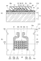
- FIG. 1A and FIG. 1B are schematic views illustrating the configuration of the light emitting element module substrate according to the first embodiment. That is, FIG. 1B is a schematic plan view illustrating the configuration of the light emitting element module substrate 110 according to this embodiment.
- FIG. 1A is a schematic cross-sectional view illustrating the configuration of the light-emitting element module substrate 110, and is a cross-sectional view taken along line 1A1-1A2 of FIG.
- the light emitting element module substrate 110 includes a laminated plate 10 and a metal layer 20.
- the laminated plate 10 includes a base metal plate 11 and an insulating layer 12 provided on the base metal plate 11.
- the base metal plate 11 is made of, for example, aluminum, copper, iron, or an alloy containing two or more thereof. That is, a metal having high thermal conductivity is used for the base metal plate 11 in order to improve the heat dissipation of the light emitting element module substrate 110.
- the thickness of the base metal plate 11 can be about 0.5 mm or more and about 2 mm or less, for example.
- the thickness of the base metal plate 11 is desirably about 1 mm or more and about 1.5 mm or less, for example. In addition, this embodiment is not restricted to this, The thickness of the base metal plate 11 is arbitrary.
- a resin such as epoxy, phenol, cyanate, or polyimide can be used.
- a thermosetting resin made of bismaleimide triazine resin or the like can be used.
- a glass cloth impregnated with these resins may be used for the insulating layer 12.
- the insulating layer 12 may be, for example, a material obtained by adding a filler to these resins.
- the thermal resistance of the insulating layer 12 is set low.
- techniques such as making the insulating layer 12 thin and increasing the thermal conductivity of the insulating layer 12 are applied.
- the thickness of the insulating layer 12 is set to, for example, 150 micrometers ( ⁇ m) or less in order to obtain good thermal conductivity.
- the metal layer 20 is provided on the insulating layer 12.
- the metal layer 20 includes a mounting portion 25 on which the light emitting element is mounted, and a bonding portion 26 to which a wiring electrically connected to the light emitting element is bonded.
- the bonding part 26 can include, for example, an n-side bonding part 26n and a p-side bonding part 26p.
- one mounting portion 25 is provided, one n-side bonding portion 26n is provided, and one p-side bonding portion 26p is provided.
- the mounting portion 25 and the bonding portion 26 are provided.
- the number of (for example, the n-side bonding part 26n and the p-side bonding part 26p) is arbitrary.
- the pattern shape of the mounting portion 25 and the pattern shape of the bonding portion 26 (n-side bonding portion 26n and p-side bonding portion 26p) are arbitrary. Further, the n-side bonding part 26n and the p-side bonding part 26p can be interchanged with each other.
- the light emitting element for example, a semiconductor light emitting element such as an LED element is used.
- the metal layer 20 includes a silver layer 23 that is the uppermost layer of at least one of the mounting portion 25 and the bonding portion 26.
- the silver layer 23 is the uppermost layer of both the mounting portion 25 and the bonding portion 26.
- the metal layer 20 further includes a base layer 21 provided between the silver layer 23 and the insulating layer 12.
- the metal layer 20 can further include an intermediate layer 22 provided between the base layer 21 and the silver layer 23. That is, in this specific example, the metal layer 20 has a laminated structure of a base layer 21, an intermediate layer 22 provided thereon, and a silver layer 23 provided thereon and serving as the uppermost layer of the metal layer 20. Have.
- the underlayer 21 can contain, for example, copper (Cu). That is, a Cu layer can be used for the base layer 21.
- Cu copper
- the present embodiment is not limited to this, and the material used for the base layer 21 is arbitrary.
- the intermediate layer 22 can include at least one of nickel (Ni) and palladium (Pd). That is, the intermediate layer 22 can be any one of a Ni layer, a Pd layer, and a layer containing Ni and Pd. However, this embodiment is not limited to this, and the material used for the intermediate layer 22 is arbitrary.
- the silver layer 23 is formed by, for example, electrolytic plating. That is, the foundation layer 21 is used as an electrode layer in electrolytic plating.
- the intermediate layer 22 functions as a barrier layer.
- a component for example, Cu
- middle layer 22 is provided as needed and can be abbreviate
- the intermediate layer 22 can be a Ni layer formed by electrolytic plating.
- the main component of the intermediate layer 22 is Ni, and the intermediate layer 22 does not substantially contain phosphorus (P).
- the intermediate layer 22 contains phosphorus in addition to Ni.
- the phosphorus ratio in the intermediate layer 22 is about 8% to 10% (Ni ratio is about 90% to 82%). This is because when a Ni layer is formed by electroless plating, a plating film deposition phenomenon due to the reduction action of hypophosphorous acid is used.
- the thickness of the silver layer 23 is, for example, 1 ⁇ m or more. Thereby, as will be described later, the silver layer 23 can have a high reflectance and a high bonding property. That is, in the present embodiment, the metal layer 20 can have a high reflectance and a high bonding property.
- the mounting part 25 and the bonding part 26 are electrically cut off from the peripheral edge 10e of the laminated plate 10. Specifically, the mounting part 25 and the bonding part 26 are separated from the peripheral edge 10e of the laminated board 10, and the distance between the mounting part 25 and the bonding part 26 and the peripheral edge 10e of the laminated board 10 is electrically It is set at a sufficient distance to be blocked.
- a solder resist layer 40 is provided on a portion of the upper surface of the insulating layer 12 where the metal layer 20 is not provided.
- a white material is used for the solder resist layer 40.
- FIG. 2A and FIG. 2B are schematic views illustrating the usage state of the light emitting element module substrate according to the first embodiment. That is, these drawings illustrate a state where the LED element is mounted on the light emitting element module substrate 110 and the light emitting element module 210 is formed. That is, FIG. 2B is a schematic plan view illustrating the configuration of the light emitting element module 210.
- FIG. 2A is a schematic cross-sectional view illustrating the configuration of the light-emitting element module 210, and is a cross-sectional view taken along line 2A1-2A2 of FIG.
- the light emitting element module 210 includes a light emitting element module substrate 110 according to this embodiment and a light emitting element mounted on the mounting portion 25 of the light emitting element module substrate 110. 50 and bonding wiring 51 (wiring) for electrically connecting the light emitting element 50 and the bonding portion 26.
- an LED element is used as the light emitting element 50.
- a plurality of light emitting elements 50 are used, but the number of light emitting elements 50 is arbitrary.
- Each of the light emitting elements 50 has, for example, a p-side electrode and an n-side electrode (not shown).
- the n-side electrode is electrically connected to the n-side bonding part 26n or the p-side electrode of another light emitting element 50 by the bonding wiring 51, for example.
- the p-side electrode is electrically connected to the p-side bonding part 26p or the n-side electrode of another light emitting element 50 by the bonding wiring 51, for example.
- the metal layer 20 is further provided with a power supply unit 26 c that is electrically connected to the bonding unit 26.
- a power supply unit 26 c that is electrically connected to the bonding unit 26.
- an external connector is attached to the power supply unit 26c, and an external power supply wiring is connected to the power supply unit 26c by, for example, a method such as soldering. Then, power is supplied to the light emitting element 50 to cause the light emitting element 50 to emit light.
- the light emitting element module substrate 110 is provided with an attachment portion 13.
- the light emitting element module substrate 110 is attached to the heat radiating member of the illuminating device to be described later by the attaching portion 13 by a technique such as screwing.
- the light emitting element module 210 may further include a wavelength conversion layer 60 that covers at least a part of the light emitting element 50.
- the wavelength conversion layer 60 absorbs the emitted light emitted from the light emitting element 50 and emits light having a wavelength different from the wavelength of the emitted light.
- a phosphor layer can be used for the wavelength conversion layer 60.
- Part of the emitted light emitted from the light emitting element 50 travels to the upper surface side (the side opposite to the laminated plate 10) of the light emitting element 50, passes through the wavelength conversion layer 60, and is converted in wavelength. It is taken out of the module 210.
- Another part of the emitted light emitted from the light emitting element 50 proceeds to the lower surface side (the laminated plate 10 side) of the light emitting element 50, is reflected by the metal layer 20, and proceeds toward the wavelength conversion layer 60.
- the wavelength is converted through the wavelength conversion layer 60 and is taken out of the light emitting element module 210.
- the silver layer 23 is provided as the uppermost layer of the metal layer 20, the emitted light emitted from the light emitting element 50 is efficiently reflected by the metal layer 20, and the light emission efficiency is high.
- the silver layer 23 is used as the uppermost layer of the metal layer 20, the bonding property between the bonding portion 26 and the bonding wiring 51 is good.
- the mounting portion 25 and the bonding portion 26 are electrically disconnected from the peripheral edge 10e of the laminated plate 10. For this reason, the mounting part 25 and the bonding part 26 are electrically insulated sufficiently from the end part.
- the light emitting element module substrate 110 it is possible to provide a light emitting element module substrate having a mounting portion and a bonding portion that have high reflectivity, high bonding properties, and excellent electrical insulation from the end portions.
- FIG. 3A, FIG. 3B, FIG. 4A, FIG. 4B, FIG. 5A, and FIG. 5B show the manufacture of the light-emitting element module substrate according to the first embodiment.
- 3B is a schematic plan view illustrating one process of the method for manufacturing the light emitting element module substrate 110
- FIG. 3A is a cross-sectional view taken along line 3A1-3A2 of FIG. 3B.
- FIG. 4B is a schematic plan view illustrating a step after the steps illustrated in FIGS. 3A and 3B.
- FIG. 4A is a schematic plan view of FIG.
- FIG. 4 is a sectional view taken along line 4A1-4A2.
- FIG. 5B is a schematic plan view illustrating a step after the steps illustrated in FIGS. 4A and 4B.
- FIG. 5A is a schematic plan view illustrating the step after FIG.
- FIG. 5 is a sectional view taken along line 5A1-5A2.
- the silver layer 23 is formed by electrolytic plating.
- the solder resist layer 40 is omitted.
- the base layer 21 having a predetermined shape is formed on the insulating layer 12 of the laminated plate 10.
- the underlayer 21 has a portion 25 a corresponding to the mounting portion 25 and a portion 26 a corresponding to the bonding portion 26.
- the base layer 21 is for mounting portion plating wiring portion 27 for performing electrolytic plating on the portion 25 a corresponding to the mounting portion 25 and for bonding portion plating for performing electrolytic plating on the portion 26 a corresponding to the bonding portion 26.
- a wiring portion 28 is provided in FIGS. 3A and 3B.
- a metal layer is formed in a pattern in which a plurality of final light emitting element module substrates 110 are arranged on a large area laminate, and then the metal layer and the laminate are divided to produce a plurality of light emission.
- the element module substrates 110 are manufactured in a lump.
- the present embodiment is not limited to this, and a method of separately forming the light emitting element module substrates 110 one by one may be adopted.
- the intermediate layer 22 is formed on the base layer 21 by electrolytic plating, and the silver layer 23 is electrolyzed on the intermediate layer 22. It is formed by plating. Thereby, the mounting part 25 and the bonding part 26 of the metal layer 20 are formed.
- middle layer 22 may be abbreviate
- the intermediate layer 22 is formed so as to cover the upper surface and the side surface of the base layer 21. Further, a silver layer 23 is formed so as to cover the upper surface and side surfaces of the intermediate layer 22.
- middle layer 22 may be abbreviate
- the intermediate layer 22 and the silver layer 23 are also formed on the mounting portion plating wiring portion 27 and the bonding portion plating wiring portion 28 of the base layer 21.
- the intermediate layer 22 may be omitted in some cases.
- a silver layer is formed on the mounting portion plating wiring portion 27 and the bonding portion plating wiring portion 28 of the base layer 21. 23 is formed.
- the mounting portion plating wiring portion 27 and the bonding portion plating wiring portion 28 are removed by, for example, etching using a mask. That is, the base layer 21, the intermediate layer 22 and the silver layer 23 corresponding to the mounting part plating wiring part 27 are removed, and the base layer 21, the intermediate layer 22 and the silver layer 23 corresponding to the bonding part plating wiring part 28 are removed. To do.
- the base layer 21 and the intermediate layer 22 are exposed on the end face (end portion 26e) of the metal layer 20 in the portion connected to the removed mounting portion plating wiring portion 27 and bonding portion plating wiring portion 28. To do.
- the base layer 21 is exposed on at least a part of the side surface of the metal layer 20 (the end portion 26e in this example).
- the intermediate layer 22 is provided, the base layer 21 and the intermediate layer 22 are exposed on at least a part of the side surface of the metal layer 20.
- the laminated plate 10 is cut into a predetermined size, and further, the attachment portion 13 is formed as necessary, whereby the light emitting element module substrate 110 is manufactured.
- the silver layer 23 that is the uppermost layer of the metal layer 20 is formed by electrolytic plating, and is used for electrolytic plating of the metal layer 20. At least a part of the plating wiring part (mounting part plating wiring part 27 and bonding part plating wiring part 28) is removed. Thereby, the mounting part 25 and the bonding part 26 are electrically cut off from the peripheral edge 10e of the laminated plate 10.
- the characteristics of the light emitting element module substrate 110 according to the present embodiment will be described. That is, the characteristics of the metal layer 20, particularly the silver layer 23, will be described.
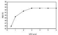
- FIG. 6 is a graph illustrating characteristics of the light emitting element module substrate according to the first embodiment. That is, this figure illustrates the measurement result of the relationship between the thickness t23 of the silver layer 23 and the reflectance R23.
- the horizontal axis is the thickness t23 of the silver layer 23, and the vertical axis is the reflectance R23 of the silver layer 23 when the wavelength is 460 nanometers (nm).
- a Ni plating layer having a thickness of 5 ⁇ m is provided under the silver layer 23.
- the reflectance R23 is 86% and the reflectance R23 is low.
- the reflectance R23 increases.
- the reflectance R23 is as high as 89.5%.
- the thickness t23 is 2 ⁇ m, the reflectance R23 is further increased to 91.6%.
- the thickness t23 increases, and when the thickness is about 3 ⁇ m or more, the reflectance R23 is constant at about 93%.
- the thickness t23 of the silver layer 23 is thicker.
- the thickness t23 of the silver layer 23 is desirably 1 ⁇ m or more. Thereby, high reflectance R23 is obtained.
- the thickness t23 of the silver layer 23 is desirably 2 ⁇ m or more. Thereby, higher reflectance R23 is obtained.
- the thickness t23 of the silver layer 23 is preferably 3 ⁇ m or more. As a result, a higher and more stable reflectance R23 can be obtained.
- the method using electroless plating is also considered as a formation method of the silver layer 23
- the thickness t23 of the silver layer 23 by electroless plating is less than 1 micrometer, for example, is about 0.5 micrometer or less.
- an electrolytic plating method is employed in forming the silver layer 23.
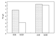
- FIG. 7 is a graph illustrating characteristics of the light emitting element module substrate according to the first embodiment. That is, this figure illustrates the measurement results of the bonding characteristics when the thickness t23 of the silver layer 23 is 0.5 ⁇ m and 2.0 ⁇ m.
- the vertical axis represents the wire pull strength PS (gf).
- the state h119 after heat treatment at 180 ° C. for 60 minutes
- the initial state i110 when the thickness t23 of the silver layer 23 is 2 ⁇ m.
- the wire pull strength PS in the state h110 after heat treatment at 180 ° C. for 60 minutes is illustrated.
- the case where the thickness t23 of the silver layer 23 is 0.5 ⁇ m corresponds to a comparative example, and the case where the thickness t23 of the silver layer 23 is 2 ⁇ m corresponds to an example of this embodiment.
- a Ni plating layer having a thickness of 5 ⁇ m is provided under the silver layer 23.
- the wire pull strength PS is about 6.5 gf, which is small. In the state h119 after the heat treatment, the wire pull strength PS is about 3 gf, which is greatly reduced.
- the wire pull strength PS is about 8.2 gf, which is higher than when the thickness t23 is 0.5 ⁇ m.
- the wire pull strength PS is about 8.0 gf, which is almost the same as that in the initial state i110. Very small compared to the example.
- the wire pull strength PS is small and is significantly reduced by heat treatment, whereas the thickness t23 of the silver layer 23 is 2 ⁇ m.
- the wire pull strength PS is very large, and the decrease due to heat treatment is also suppressed.
- the thickness t23 of the silver layer 23 when the thickness t23 of the silver layer 23 is large, the wire pull strength PS is increased, and the bondability is improved. For this reason, it is desirable for the thickness t23 of the silver layer 23 to be 1 ⁇ m or more, whereby high bonding properties can be obtained. Furthermore, the thickness t23 of the silver layer 23 is desirably 2 ⁇ m or more. Thereby, higher bondability can be obtained.
- FIG. 8A and FIG. 8B are diagrams illustrating characteristics of the light emitting element module substrate according to the first embodiment. That is, FIG. 8A illustrates the result of measuring the withstand voltage when the distance between the conductive layer 20 a provided on the insulating layer 12 of the laminated plate 10 and the end of the laminated plate 10 is changed. FIG. 8B is a schematic cross-sectional view illustrating the above measurement conditions.
- a base metal plate 11 and an insulating layer 12 laminated thereon are provided in the laminated plate 10.
- the thickness of the base metal plate 11 is 1 mm
- the thickness of the insulating layer 12 is 80 ⁇ m.
- a conductive layer 20 a is provided on the insulating layer 12.
- the conductive layer 20 a corresponds to the metal layer 20.
- a copper layer having a thickness of 35 ⁇ m is used for the conductive layer 20a.
- the withstand voltage BV was measured by changing the distance d20a between the conductive layer 20a and the end (periphery 10e) of the laminated plate 10.
- the withstand voltage BV is a withstand voltage related to alternating current.
- FIG. 8A is a graph illustrating the measurement result of the withstand voltage BV, and the horizontal axis is the distance d20a between the conductive layer 20a and the end (periphery 10e) of the laminated plate 10, and the vertical axis The axis is the withstand voltage BV.
- the withstand voltage BV increases as the distance d20a between the conductive layer 20a and the end (periphery 10e) of the laminated plate 10 increases.
- the withstand voltage BV is about 1.4 kilovolts (kV).
- the withstand voltage BV is about 2.5 kV and when the distance d20a is 3 mm.
- the withstand voltage BV is about 3.2 kV.
- the withstand voltage BV also depends on the thickness of the insulating layer 12, for example. In general, the withstand voltage BV increases as the thickness of the insulating layer 12 increases. However, generally, when the thickness of the insulating layer 12 is increased, the thermal conductivity of the laminated plate 10 is lowered and the heat dissipation is lowered. For this reason, the thickness of the insulating layer 12 is set to an appropriate value in consideration of heat dissipation.
- the insulating layer 12 may be made of a resin added with a filler in order to increase the heat dissipation of the light emitting element module substrate 110. Since the thermal conductivity of the resin is generally about 0.2 W / mK, the insulating layer 12 may be obtained by adding a filler with high thermal conductivity such as alumina or BN to the resin. it can. Thereby, for example, a thermal conductivity of about 1 W / mK or more and 6 W / mK or less can be obtained.
- the thermal resistance of the insulating layer 12 decreases, but the withstand voltage of the light emitting element module substrate 110 tends to decrease accordingly. Therefore, in order to obtain the withstand voltage performance required when applied to a lighting device, the specification of the insulating layer 12 is appropriately set in consideration of the withstand voltage performance and the heat dissipation performance.
- the distance d20a is appropriately set so as to obtain a necessary withstand voltage BV while conforming to the set thickness of the insulating layer 12.
- the mounting portion 25 and the bonding portion 26 are electrically cut off from the peripheral edge 10e of the laminated plate 10. That is, the mounting part 25 and the bonding part 26 are separated from the peripheral edge 10e. Then, the end of the conductive layer electrically connected to the mounting portion 25 and the bonding portion 26 on the side of the peripheral edge 10e of the laminated plate 10 is separated from the peripheral edge 10e.
- the distance between the edge of the conductive layer on the peripheral edge 10e side and the peripheral edge 10e is set based on, for example, the relationship between the distance d20a illustrated in FIG. 8A and the withstand voltage BV.
- the silver layer 23 of the metal layer 20 is set to a thickness of 1 ⁇ m or more (preferably 2 ⁇ m or more), so that a high reflectance and a high reflectivity are achieved. Bondability can be obtained.
- a thick silver layer 23 can be formed by an electrolytic plating method, and the plating wiring portion (mounting portion plating wiring portion 27 and bonding portion plating wiring portion 28) used for the electrolytic plating is used. By removing at least a part, the mounting portion 25 and the bonding portion 26 are sufficiently electrically disconnected from the end portion (periphery 10e) of the laminated plate 10.
- the withstand voltage BV of 1 kV or more can be obtained by electrically interrupting the mounting part 25 and the bonding part 26 from the end part (periphery 10e) of the laminated board 10, for example.
- the pattern shape of the metal layer 20 is arbitrary as long as the mounting portion 25 and the bonding portion 26 are electrically cut off from the peripheral edge 10e of the laminated plate 10.
- FIG. 9A to FIG. 9D are schematic plan views illustrating the configuration of another light emitting element module substrate according to the first embodiment.
- the plating wiring portion (mounting portion plating wiring) used for the electrolytic plating is used. At least a part of the portion 27 and the bonding portion plating wiring portion 28) is removed.
- the portion on the peripheral edge 10e side of the plating wiring portion is removed. And the part inside the wiring part for plating remains. Other than this, since it is the same as the light emitting element module substrate 110, the description is omitted.
- the end portion 28e) of the wiring portion 28 for use is sufficiently separated from the peripheral edge 10e.
- the mounting part 25 and the bonding part 26 are electrically cut off from the peripheral edge 10e of the laminated plate 10.
- the inner part of the plating wiring part far from the peripheral edge 10e is removed, and the plating wiring part is divided in the middle. And the part of the outer side (edge 10e side) of the wiring part for plating remains. Other than this, since it is the same as the light emitting element module substrate 110, the description is omitted.
- the plating wiring part is divided, and the plating wiring part, the mounting part 25, and the bonding part 26 are electrically disconnected, so that the mounting part 25 and the bonding part 26 are The laminate 10 is electrically cut off from the peripheral edge 10e.
- the inner portion of the mounting portion plating wiring portion 27 far from the peripheral edge 10e is removed, and the plating wiring portion is divided in the middle. Further, in the bonding portion plating wiring portion 28 connected to the n-side bonding portion 26n, the portion on the peripheral edge 10e side is removed. Further, in the bonding part plating wiring part 28 connected to the p-side bonding part 26p, the intermediate part between the peripheral edge 10e and the inner part is removed.
- the plating wiring part is divided, and the plating wiring part, the mounting part 25, and the bonding part 26 are electrically disconnected, so that the mounting part 25 and the bonding part 26 are The laminate 10 is electrically cut off from the peripheral edge 10e.
- the portion of the metal layer 20 where the wiring portion for plating used for electrolytic plating is removed is arbitrary.
- the portion 27f connected to the mounting portion plating wiring portion 27 is removed from the mounting portion 25, and the mounting portion plating wiring portion 27 and the mounting portion are removed. 25 is divided. Further, in the n-side bonding portion 26n, the portion 28nf connected to the bonding portion plating wiring portion 28 is removed, and the bonding portion plating wiring portion 28 and the n-side bonding portion 26n are separated. Further, the bonding portion plating wiring portion 28 connected to the p-side bonding portion 26p is removed, and further, the portion 28pf connected to the bonding portion plating wiring portion 28 is removed from the p-side bonding portion 26p. ing. Thus, the part connected to the wiring part for plating at least one of the mounting part 25 and the bonding part 26 may be removed.
- the plating wiring part, the mounting part 25, and the bonding part 26 are separated from each other, and the plating wiring part, the mounting part 25, and the bonding part 26 are electrically cut off.
- the mounting portion 25 and the bonding portion 26 are electrically disconnected from the peripheral edge 10e of the laminated plate 10.
- the part to be removed of the plating wiring part used for the electrolytic plating is arbitrary.
- the position and shape of the part which was connected to the wiring part for plating of the mounting part 25 and the bonding part 26, and is removed are arbitrary.
- a light emitting element module substrate having the mounting portion 25 and the bonding portion 26 that have high reflectivity, high bonding properties, and excellent electrical insulation from the end portions can be obtained.
- FIG. 10 is a schematic cross-sectional view illustrating the configuration of another light emitting element module substrate according to the first embodiment. That is, FIG. 10 is a cross-sectional view taken along line 10A1-10A2 of FIG.
- the portion on the peripheral edge 10e side of the plating wiring portion (for example, the bonding portion plating wiring portion 28) is removed, and the plating wiring portion (for example, bonding) The inner part of the partial plating wiring part 28) remains.
- the underlying layer 21 is exposed at the end of the remaining part of the plating wiring part on the side of the peripheral edge 10e of the laminate 10 (for example, the end part 28e of the bonding part plating wiring part 28).
- the intermediate layer 22 is provided, and the end of the remaining plating wiring portion on the side of the peripheral edge 10e of the laminated plate 10 (for example, the end of the bonding portion plating wiring portion 28). In 28e), the underlayer 21 and the intermediate layer 22 are exposed.
- the formation 21 is exposed.
- the base layer 21 and the intermediate layer 22 are exposed.
- the base layer 21 is exposed on at least a part of the side surface of the metal layer 20.
- the base layer 21 is exposed on at least a part of the side surface of the metal layer 20.
- the silver layer 23 is formed by electrolytic plating, and at least a part of the wiring portion for plating used for electrolytic plating in the metal layer 20 is removed after electrolytic plating. Therefore, the base layer 21 is exposed on at least a part of the side surface of the metal layer 20.
- the wiring portion for plating is not provided, so that the upper surface and side surfaces of the base layer 21 are covered with the intermediate layer 22, and the upper surface of the intermediate layer 22 and The side surface is covered with a silver layer 23. For this reason, the base layer 21 is not exposed on the side surface of the metal layer 20.
- the second embodiment is a light emitting element module 210 using the light emitting element module substrate 110 according to the embodiment.
- the configuration of the light emitting element module 210 according to the present embodiment is as already described with reference to FIGS. 2 (a) and 2 (b). That is, the light emitting element module 210 includes any one of the light emitting element module substrates according to the embodiment (for example, at least one of the light emitting element module substrates 110 and 110a to 110d).
- the case where the light emitting element module substrate 110 is used will be described.
- the light emitting element module 210 includes the light emitting element 50 mounted on the mounting portion 25 of the light emitting element module substrate 110, the light emitting element 50, and the bonding portion 26. And a bonding wiring 51 that is electrically connected.
- the light emitting element 50 for example, an LED element using a nitride semiconductor is used.
- the bonding wiring 51 any one of gold, silver, aluminum, and copper, and an alloy including two or more thereof are used.
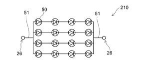
- FIG. 11 is a circuit diagram illustrating the configuration of the light emitting element module according to the second embodiment.
- a plurality of light emitting elements 50 are connected in series and in parallel by bonding wires 51.
- 16 light emitting elements 50 are used, and 4 series and 4 parallel circuit configurations are applied.
- the present embodiment is not limited to this, and the number of light emitting elements 50 and the applied circuit configuration are arbitrary.
- the light emitting element module 210 may further include a wavelength conversion layer 60 that covers at least a part of the light emitting element 50.
- the wavelength conversion layer 60 absorbs the emitted light emitted from the light emitting element 50 and emits light having a wavelength different from the wavelength of the emitted light.
- the wavelength conversion layer 60 is formed by a method such as coating. Thereby, for example, white light is obtained.
- the present embodiment is not limited to this, and the wavelength conversion layer 60 may be provided as necessary and may be omitted.
- LED elements for example, three types of light emitting elements 50 (for example, LED elements) that emit blue, green, and red light respectively are used. This method may be applied to the light emitting element module 210.
- a method of obtaining white light emission for example, there is a method of combining a light emitting element 50 (for example, an LED element) that emits blue light and a phosphor that emits at least one of yellow and orange light. You may apply to 210.
- a light emitting element 50 for example, an LED element
- a phosphor that emits at least one of yellow and orange light. You may apply to 210.
- a method of obtaining white light emission for example, there is a method of combining a light emitting element 50 (LED element) that emits ultraviolet light and, for example, three types of phosphors that emit blue, green, and red, respectively. May be applied to the light emitting element module 210. As described above, when the phosphor is used, the wavelength conversion layer 60 is provided.
- LED element light emitting element 50
- three types of phosphors that emit blue, green, and red, respectively.
- a plurality of LED elements are mounted on, for example, a light emitting element module substrate according to a required light flux.
- the method of mounting the LED element on the light emitting element module substrate includes, for example, a method of mounting a package including the LED element on the light emitting element module substrate by soldering, and a wire bonding of the LED element chip directly to the light emitting element module substrate. For example, there is a method of mounting (COB configuration).
- the wavelength conversion layer 60 is provided by applying a resin mixed with a phosphor on the plurality of light emitting elements 50 (LED elements) mounted on the light emitting element module substrate 110.
- illumination with a desired color temperature can be realized.
- not only white but light of arbitrary colors can be obtained.
- the LED element In the LED element, a part of the input electric energy is changed to light energy, and the other part is consumed as heat. For this reason, the temperature of the LED element rises during operation. When the LED element reaches a high temperature, for example, the deterioration of the LED element progresses and the life is shortened. Furthermore, as already described, the LED element has high luminous efficiency at low temperatures and low luminous efficiency at high temperatures. For this reason, in the illuminating device using an LED element, heat countermeasures are important, and the light emitting element module substrate 110 is required to have sufficiently high heat dissipation.
- the base metal plate 11 for the laminated plate 10 on which the light emitting element 50 is mounted by using the base metal plate 11 for the laminated plate 10 on which the light emitting element 50 is mounted, high heat dissipation can be realized, and high Luminous efficiency and good lifetime can be realized.
- the light emitting element module 210 is required to have sufficient performance regarding basic insulation from the viewpoint of preventing the destruction of the LED element due to a voltage such as a surge and the safety of the product.
- a withstand voltage is applied to the lighting circuit that is a charging unit and the appliance main body that is a non-charging unit.
- the performance with respect to basic insulation is evaluated depending on whether it can sufficiently withstand. Note that the value of the withstand voltage varies depending on the input voltage of the lighting device, and the higher the input voltage, the more basic insulation with respect to the higher withstand voltage is required. For example, in a lighting device using the light emitting element module 210, a withstand voltage of 1 kV or more is generally required.
- the mounting portion 25 and the bonding portion 26 are electrically disconnected from the peripheral edge 10e of the laminated plate 10, a withstand voltage of 1 kV or more can be realized.
- FIG. 12 is a schematic cross-sectional view illustrating the configuration of the illumination device according to the third embodiment.
- the illumination device 310 according to the present embodiment is thermally connected to the light emitting element module 210 according to the embodiment and the base metal plate 11 of the light emitting element module substrate 110 included in the light emitting element module 210.
- the heat radiating member 321 is provided.
- a metal material such as aluminum die cast is used.
- the attachment of the base metal plate 11 (laminated plate 10) to the heat radiating member 321 for example, a method such as screwing using the attachment portion 13 can be employed.
- this embodiment is not limited to this, and the attachment method is arbitrary.
- heat generated by the light emitting element 50 is efficiently transmitted to the heat dissipation member 321 via the base metal plate 11 by thermally connecting the heat dissipation member 321 and the base metal plate 11. High heat dissipation.
- the lighting device of this specific example is a light bulb type lighting device, but the form of the lighting device is arbitrary, and for example, a downlight type or a mini-krypton type can be adopted, and for example, a backlight. It can also be applied to lighting devices such as lamps and headlamps.
- the illuminating device 310 employs the light emitting element module 210 using the light emitting element module substrate 110 according to the embodiment, so that it has high reflectivity and high bonding properties and is excellent in electrical insulation from the end. Therefore, a lighting device having high efficiency, low power consumption, high reliability, and high operational stability can be realized.
- a light-emitting element included in a light-emitting element module such as a laminated plate, a base metal plate, an insulating layer, a metal layer, a silver layer, an underlayer, an intermediate layer, a plating wiring portion, and a solder resist layer
- a person skilled in the art has made various changes regarding the shape, size, material, arrangement relationship, etc. of the specific configuration of each element such as the wiring and wavelength conversion layer and the heat dissipation member included in the lighting device.
- the present invention is also included in the scope of the present invention as long as the present invention can be carried out in the same manner and the same effects can be obtained by appropriately selecting from a known range. Moreover, what combined any two or more elements of each specific example in the technically possible range is also included in the scope of the present invention as long as the gist of the present invention is included.
Landscapes
- Engineering & Computer Science (AREA)
- Manufacturing & Machinery (AREA)
- Microelectronics & Electronic Packaging (AREA)
- Led Device Packages (AREA)
- Led Devices (AREA)
- Arrangement Of Elements, Cooling, Sealing, Or The Like Of Lighting Devices (AREA)
- Non-Portable Lighting Devices Or Systems Thereof (AREA)
Abstract
La présente invention se rapporte à un substrat de module d'élément électroluminescent qui est pourvu d'une carte stratifiée et d'une couche métallique. La carte stratifiée comprend une plaque métallique de base et une couche isolante disposée sur la plaque métallique de base. La couche métallique est disposée sur la couche isolante. La couche métallique présente une section de montage sur laquelle est monté un élément électroluminescent, et une section de liaison à laquelle est relié un câblage raccordé électriquement à l'élément électroluminescent. La couche métallique est la couche supérieure de la section de montage et/ou de la section de liaison, et comprend une couche d'argent formée par placage électrolytique. La section de montage et la section de liaison sont protégées électriquement de la périphérie de la carte stratifiée.
Priority Applications (4)
| Application Number | Priority Date | Filing Date | Title |
|---|---|---|---|
| EP11762430A EP2555264A1 (fr) | 2010-03-31 | 2011-02-25 | Substrat de module d'élément électroluminescent, module d'élément électroluminescent et dispositif d'éclairage |
| US13/635,993 US20130037834A1 (en) | 2010-03-31 | 2011-02-25 | Light emitting element module substrate, light emitting element module, and illuminating device |
| CN2011900000410U CN202905785U (zh) | 2010-03-31 | 2011-02-25 | 发光元件模块基板、发光元件模块及照明装置 |
| US14/329,212 US20140322841A1 (en) | 2010-03-31 | 2014-07-11 | Light emitting element module substrate, light emitting element module, and illuminating device |
Applications Claiming Priority (2)
| Application Number | Priority Date | Filing Date | Title |
|---|---|---|---|
| JP2010-081911 | 2010-03-31 | ||
| JP2010081911A JP2011216588A (ja) | 2010-03-31 | 2010-03-31 | 発光素子モジュール基板、発光素子モジュール及び照明装置 |
Related Child Applications (2)
| Application Number | Title | Priority Date | Filing Date |
|---|---|---|---|
| US13/635,993 A-371-Of-International US20130037834A1 (en) | 2010-03-31 | 2011-02-25 | Light emitting element module substrate, light emitting element module, and illuminating device |
| US14/329,212 Continuation US20140322841A1 (en) | 2010-03-31 | 2014-07-11 | Light emitting element module substrate, light emitting element module, and illuminating device |
Publications (1)
| Publication Number | Publication Date |
|---|---|
| WO2011122190A1 true WO2011122190A1 (fr) | 2011-10-06 |
Family
ID=44711922
Family Applications (1)
| Application Number | Title | Priority Date | Filing Date |
|---|---|---|---|
| PCT/JP2011/054321 Ceased WO2011122190A1 (fr) | 2010-03-31 | 2011-02-25 | Substrat de module d'élément électroluminescent, module d'élément électroluminescent et dispositif d'éclairage |
Country Status (6)
| Country | Link |
|---|---|
| US (2) | US20130037834A1 (fr) |
| EP (1) | EP2555264A1 (fr) |
| JP (1) | JP2011216588A (fr) |
| CN (1) | CN202905785U (fr) |
| TW (1) | TWI479705B (fr) |
| WO (1) | WO2011122190A1 (fr) |
Cited By (1)
| Publication number | Priority date | Publication date | Assignee | Title |
|---|---|---|---|---|
| TWI469405B (zh) * | 2012-08-17 | 2015-01-11 | 復盛精密工業股份有限公司 | 熱固型發光二極體的支架結構製作方法 |
Families Citing this family (8)
| Publication number | Priority date | Publication date | Assignee | Title |
|---|---|---|---|---|
| JP5984199B2 (ja) * | 2011-12-26 | 2016-09-06 | シチズン電子株式会社 | 発光装置 |
| WO2014038169A1 (fr) * | 2012-09-06 | 2014-03-13 | シャープ株式会社 | Substrat d'élément électroluminescent et procédé de fabrication de celui-ci |
| JP6138814B2 (ja) * | 2012-10-24 | 2017-05-31 | シャープ株式会社 | 発光装置および発光装置の製造方法 |
| JP6104946B2 (ja) * | 2013-01-24 | 2017-03-29 | シャープ株式会社 | 発光装置およびその製造方法 |
| JP6402914B2 (ja) * | 2013-11-29 | 2018-10-10 | 日亜化学工業株式会社 | 発光装置の製造方法 |
| FR3028920A1 (fr) * | 2014-11-25 | 2016-05-27 | Bell & Wyson | Ampoule d’eclairage munie d’un dispositif additionnel |
| KR102473668B1 (ko) | 2016-03-02 | 2022-12-01 | 삼성전자주식회사 | 발광 소자 실장 기판 및 이를 이용한 발광 패키지 |
| JP3212657U (ja) * | 2017-07-13 | 2017-09-21 | 株式会社グッド・グッズ | 充電式ポータブルled投光器 |
Citations (4)
| Publication number | Priority date | Publication date | Assignee | Title |
|---|---|---|---|---|
| JP2005085912A (ja) * | 2003-09-05 | 2005-03-31 | Seiwa Electric Mfg Co Ltd | Ledランプ |
| JP2009081196A (ja) * | 2007-09-25 | 2009-04-16 | Sanyo Electric Co Ltd | 発光モジュールおよびその製造方法 |
| JP2009111273A (ja) | 2007-10-31 | 2009-05-21 | Toshiba Lighting & Technology Corp | 発光装置 |
| JP2009302127A (ja) * | 2008-06-10 | 2009-12-24 | Dainippon Printing Co Ltd | Led用基板、led実装モジュール、およびled用基板の製造方法 |
Family Cites Families (15)
| Publication number | Priority date | Publication date | Assignee | Title |
|---|---|---|---|---|
| JPS61272978A (ja) * | 1985-05-28 | 1986-12-03 | Takiron Co Ltd | ドツトマトリクス発光表示体に於けるマトリクス回路基板 |
| JPH0443698A (ja) * | 1990-06-11 | 1992-02-13 | Matsushita Electric Ind Co Ltd | 多層積層配線基板 |
| JP2000151077A (ja) * | 1998-11-13 | 2000-05-30 | Sumitomo Osaka Cement Co Ltd | 高密度配線基板の製造方法 |
| US6350386B1 (en) * | 2000-09-20 | 2002-02-26 | Charles W. C. Lin | Method of making a support circuit with a tapered through-hole for a semiconductor chip assembly |
| JP2002198639A (ja) * | 2000-12-26 | 2002-07-12 | Matsushita Electric Ind Co Ltd | プリント配線板とその製造方法および電子部品の実装方法 |
| US7091589B2 (en) * | 2002-12-11 | 2006-08-15 | Dai Nippon Printing Co., Ltd. | Multilayer wiring board and manufacture method thereof |
| JP4072519B2 (ja) * | 2004-06-18 | 2008-04-09 | シャープ株式会社 | 表示装置用照明装置 |
| JP4436265B2 (ja) * | 2005-02-16 | 2010-03-24 | 日本特殊陶業株式会社 | 発光素子実装用配線基板 |
| JP2008016593A (ja) * | 2006-07-05 | 2008-01-24 | Ngk Spark Plug Co Ltd | 発光素子搭載用配線基板 |
| JP4367457B2 (ja) * | 2006-07-06 | 2009-11-18 | パナソニック電工株式会社 | 銀膜、銀膜の製造方法、led実装用基板、及びled実装用基板の製造方法 |
| JP4980152B2 (ja) * | 2007-06-19 | 2012-07-18 | シャープ株式会社 | 照明装置 |
| JP2009170561A (ja) * | 2008-01-15 | 2009-07-30 | Panasonic Corp | 配線基板およびその製造方法 |
| JP5499325B2 (ja) * | 2009-06-01 | 2014-05-21 | 東芝ライテック株式会社 | 発光モジュールおよび照明装置 |
| TWI411143B (en) * | 2009-06-26 | 2013-10-01 | Led package structure with a plurality of standby pads for increasing wire-bonding yield and method for manufacturing the same | |
| TWM374538U (en) * | 2009-09-03 | 2010-02-21 | Wen-Lung Chin | High-efficiency LED (light emitting diode) lamp |
-
2010
- 2010-03-31 JP JP2010081911A patent/JP2011216588A/ja active Pending
-
2011
- 2011-02-25 CN CN2011900000410U patent/CN202905785U/zh not_active Expired - Fee Related
- 2011-02-25 WO PCT/JP2011/054321 patent/WO2011122190A1/fr not_active Ceased
- 2011-02-25 US US13/635,993 patent/US20130037834A1/en not_active Abandoned
- 2011-02-25 EP EP11762430A patent/EP2555264A1/fr not_active Withdrawn
- 2011-03-08 TW TW100107753A patent/TWI479705B/zh active
-
2014
- 2014-07-11 US US14/329,212 patent/US20140322841A1/en not_active Abandoned
Patent Citations (4)
| Publication number | Priority date | Publication date | Assignee | Title |
|---|---|---|---|---|
| JP2005085912A (ja) * | 2003-09-05 | 2005-03-31 | Seiwa Electric Mfg Co Ltd | Ledランプ |
| JP2009081196A (ja) * | 2007-09-25 | 2009-04-16 | Sanyo Electric Co Ltd | 発光モジュールおよびその製造方法 |
| JP2009111273A (ja) | 2007-10-31 | 2009-05-21 | Toshiba Lighting & Technology Corp | 発光装置 |
| JP2009302127A (ja) * | 2008-06-10 | 2009-12-24 | Dainippon Printing Co Ltd | Led用基板、led実装モジュール、およびled用基板の製造方法 |
Cited By (1)
| Publication number | Priority date | Publication date | Assignee | Title |
|---|---|---|---|---|
| TWI469405B (zh) * | 2012-08-17 | 2015-01-11 | 復盛精密工業股份有限公司 | 熱固型發光二極體的支架結構製作方法 |
Also Published As
| Publication number | Publication date |
|---|---|
| US20140322841A1 (en) | 2014-10-30 |
| JP2011216588A (ja) | 2011-10-27 |
| EP2555264A1 (fr) | 2013-02-06 |
| TWI479705B (zh) | 2015-04-01 |
| CN202905785U (zh) | 2013-04-24 |
| TW201214805A (en) | 2012-04-01 |
| US20130037834A1 (en) | 2013-02-14 |
Similar Documents
| Publication | Publication Date | Title |
|---|---|---|
| WO2011122190A1 (fr) | Substrat de module d'élément électroluminescent, module d'élément électroluminescent et dispositif d'éclairage | |
| JP5426481B2 (ja) | 発光装置 | |
| JP4989614B2 (ja) | 高出力ledパッケージの製造方法 | |
| JP4160881B2 (ja) | 半導体発光装置、発光モジュール、照明装置、および半導体発光装置の製造方法 | |
| KR101255121B1 (ko) | 발광 다이오드 패키지 및 그의 제조 방법 | |
| US9425373B2 (en) | Light emitting module | |
| US20110101392A1 (en) | Package substrate for optical element and method of manufacturing the same | |
| CN100539224C (zh) | 发光装置 | |
| US20110181182A1 (en) | Top view light emitting device package and fabrication method thereof | |
| JP5194675B2 (ja) | 発光装置 | |
| JP2013012694A (ja) | 発光装置及び照明装置 | |
| JP5198638B2 (ja) | 発光素子モジュール基板の製造方法 | |
| KR101719692B1 (ko) | 인쇄 회로 기판과 이의 제조방법 및 이를 이용한 led 모듈과 led 램프 | |
| JP2008244469A (ja) | 発光装置 | |
| KR102397909B1 (ko) | 기판 및 이를 포함하는 광원 모듈 | |
| JP2013201255A (ja) | 配線基板装置、発光モジュール、照明装置および配線基板装置の製造方法 | |
| US9761766B2 (en) | Chip on board type LED module | |
| JP2011258674A (ja) | 半導体発光装置及びその製造方法 | |
| CN100428512C (zh) | 发光二极管装置 | |
| KR20160083821A (ko) | 반도체 발광소자 및 이의 제조 방법 | |
| JP2006237571A (ja) | 発光ダイオード装置 | |
| KR101768908B1 (ko) | 메탈 인쇄회로기판 및 그 제조 방법, 엘이디 패키지 구조물 및 그 제조 방법 | |
| KR101264251B1 (ko) | 다층 반사면을 갖는 방열 기판 및 이를 이용한 발광 다이오드 패키지 | |
| US20140183565A1 (en) | Light-Emitting Module Board and Manufacturing Method of the Light-Emitting Module Board | |
| KR20120019697A (ko) | 발광소자 패키지 및 이를 채용한 멀티칩 조명모듈 |
Legal Events
| Date | Code | Title | Description |
|---|---|---|---|
| WWE | Wipo information: entry into national phase |
Ref document number: 201190000041.0 Country of ref document: CN |
|
| 121 | Ep: the epo has been informed by wipo that ep was designated in this application |
Ref document number: 11762430 Country of ref document: EP Kind code of ref document: A1 |
|
| WWE | Wipo information: entry into national phase |
Ref document number: 2011762430 Country of ref document: EP |
|
| NENP | Non-entry into the national phase |
Ref country code: DE |
|
| WWE | Wipo information: entry into national phase |
Ref document number: 13635993 Country of ref document: US |