WO2011125367A1 - Élément optique, et structure anti-réfléchissante et procédé pour leur production - Google Patents
Élément optique, et structure anti-réfléchissante et procédé pour leur production Download PDFInfo
- Publication number
- WO2011125367A1 WO2011125367A1 PCT/JP2011/052166 JP2011052166W WO2011125367A1 WO 2011125367 A1 WO2011125367 A1 WO 2011125367A1 JP 2011052166 W JP2011052166 W JP 2011052166W WO 2011125367 A1 WO2011125367 A1 WO 2011125367A1
- Authority
- WO
- WIPO (PCT)
- Prior art keywords
- substrate
- convex
- antireflection
- base
- antireflection structure
- Prior art date
- Legal status (The legal status is an assumption and is not a legal conclusion. Google has not performed a legal analysis and makes no representation as to the accuracy of the status listed.)
- Ceased
Links
Images





Classifications
-
- G—PHYSICS
- G02—OPTICS
- G02B—OPTICAL ELEMENTS, SYSTEMS OR APPARATUS
- G02B1/00—Optical elements characterised by the material of which they are made; Optical coatings for optical elements
- G02B1/10—Optical coatings produced by application to, or surface treatment of, optical elements
- G02B1/11—Anti-reflection coatings
- G02B1/118—Anti-reflection coatings having sub-optical wavelength surface structures designed to provide an enhanced transmittance, e.g. moth-eye structures
Definitions
- the present invention relates to an antireflection structure for preventing reflection of light, a manufacturing method thereof, and an optical element including the antireflection structure.
- Optical elements that emit or emit light include electronic devices typified by semiconductor lasers, light emitting diodes, optical sensors, solar cells, glass used in displays, optical components typified by lenses, and polarizing plates.
- an antireflection structure for the purpose of preventing light (incident light or outgoing light) incident on or emitted from the optical element from being reflected at the interface between the optical element and the outside. It is formed.
- Patent Document 1 discloses a surface treatment method using a dot array-shaped metal mask in order to form such a structure.
- Patent Document 2 discloses a method for obtaining an antireflection structure by performing reactive etching using island-shaped fine particles made of a metal body as a mask.
- Patent Document 3 discloses that a higher antireflection effect can be obtained in a moth-eye structure by forming a structure (macrostructure) larger than a wavelength of incident light and a small structure (microstructure). Is disclosed.
- the microstructure is smaller than 250 nm, and the macro structure has a size of about 10 to 100 times the wavelength of incident light.
- Patent Document 4 discloses a fine particle formation method that can form a periodic pattern of highly uniform magnetic particles at once by a simple method.
- Non-Patent Document 1 discloses a ripple shape formed on a Si substrate when the Si substrate is mounted in an ion beam sputtering apparatus and Ar ions are irradiated from an oblique direction with respect to the substrate surface. .
- Non-Patent Document 2 shows binary phase diagrams for various elements.
- Patent Document 1 discloses a method of forming a metal mask in the form of a dot array on an optical element, and performing reactive ion etching to form a weight shape on the optical element.
- the metal mask is formed. Therefore, a drawing method using an electron beam is used. Therefore, for the formation of the antireflection structure, an electron beam resist coating process on an optical substrate, an electron beam drawing process, a metal vapor deposition process, an electron beam resist removal process, a reactive ion etching process, etc.
- the thin film substance is agglomerated, decomposed, or nucleated to form metal particles in the form of islands, and this is used as a mask for reactive etching. Drawing with an electron beam as described is not required.
- thermal reaction, photoreaction, or gas reaction is required to form the metal particles into islands, and it is necessary to compare the material once formed as a thin film into islands. Since it is necessary to supply a large amount of energy, it is difficult to apply this method when the base material is formed from a material having low resistance to heat, high-intensity light, and gas.
- a step of forming one or a plurality of etching transfer layers on the substrate a step of forming a thin film material, a step of forming an island shape of the thin film material, and a reactive etching step are required.
- Patent Document 1 there arises a problem that the manufacturing process and the apparatus are complicated.
- Patent Document 3 requires a step of forming a macro structure, a step of applying a photoresist, a step of forming a microstructure by exposure, and a forming step of transmitting the structure.
- a problem that the manufacturing process and the manufacturing apparatus become complicated there arises a problem that the manufacturing process and the manufacturing apparatus become complicated.
- Patent Document 2 As described above, in the conventional technique, the process and apparatus for forming the antireflection structure are complicated, and it is difficult to easily manufacture the antireflection structure. In addition to this, the invention of Patent Document 2 also has a problem that it is difficult to apply when the substrate is made of a material having low resistance to heat, high-intensity light, and gas.
- the present invention has been made in order to solve the above-described problems, and an object of the present invention is to provide a manufacturing method and an antireflection structure capable of manufacturing an antireflection structure having a higher antireflection effect than before by a simple manufacturing method. To provide a body.
- An antireflection structure is an antireflection structure that prevents light reflection in order to solve the above-described problem, and includes a plurality of large concave portions having a plurality of small convex portions on a surface thereof.
- the pitch between the plurality of small convex portions and the pitch between the plurality of large concave portions are smaller than the wavelength of light incident on the antireflection structure.
- the antireflection structure of the present invention has a plurality of large concave portions, and a plurality of small convex portions are formed on the surface of the large concave portions.
- the width of the large concave portion is larger than the width of the small convex portion.
- the pitch between these small projections (distance between the vertices of the projections) and the pitch between large depressions (distance between the centers of the depressions) are incident light incident on the antireflection structure (in other words, Smaller than the wavelength of the light transmitted through the antireflection structure.
- the width of the small convex portion and the large concave portion is also smaller than the wavelength of the incident light.
- the presence of a plurality of large concave portions on the surface of the antireflection structure at a pitch smaller than the wavelength of incident light results in the formation of large irregularities smaller than the wavelength of incident light. Functions as a moth-eye structure.
- the antireflection structure has a moth-eye structure with small irregularities formed on the surface thereof in addition to a moth-eye structure with large irregularities.
- the antireflection effect can be enhanced as compared with the conventional configuration in which a single moth-eye structure is formed.
- the inventors of the present invention have confirmed through experiments that the antireflection effect of incident light having a wavelength ranging from the ultraviolet region to the near infrared light region can be enhanced.
- the manufacturing method of the present invention it is possible to continuously form a small convex portion and a large concave portion by continuously performing a single process, and the antireflection structure can be formed by a very simple manufacturing method.
- the body can be manufactured.
- An antireflection structure is an antireflection structure that prevents reflection of light in order to solve the above-described problem, and includes a plurality of large convex portions having a plurality of small concave portions on the surface thereof.
- the pitch between the plurality of small concave portions and the pitch between the plurality of large convex portions are smaller than the wavelength of light incident on the antireflection structure.
- the above configuration corresponds to a configuration in which the above-described antireflection structure including a plurality of small convex portions and a plurality of large concave portions is transferred to another base, and a plurality of small concave portions are formed on the surfaces of the plurality of large convex portions. It is formed and the relationship of the unevenness is reversed.
- a method for manufacturing an antireflection structure is a manufacturing method for manufacturing an antireflection structure by forming an antireflection structure on a surface of a substrate, A supply step of releasing a substrate material constituting the substrate as molecules or atoms by etching the surface and supplying a supply material that forms particles by being mixed with the substrate material from a supply source, and the supply step By forming a plurality of convex portions on the surface of the base body at a pitch smaller than the wavelength of light incident on the antireflection structure by mixing the base material released in step 1 and the supplied supply material Forming a plurality of concave portions having the convex portions on the surface, by repeating the supplying step and the convex portion forming step continuously. And characterized by forming on the surface of the substrate with again pitch.
- the base material generated by etching the surface of the base and the supply material supplied from the supply source are mixed (more preferably, chemically reacted), so that a plurality of materials are formed on the surface of the base.
- a convex part is formed.
- the plurality of convex portions are formed at a pitch smaller than the wavelength of light (incident light) incident on the antireflection structure. In other words, the distance between the vertices of the plurality of convex portions is smaller than the wavelength of the incident light.
- the unevenness formed by the plurality of protrusions and the unevenness formed by the plurality of recesses each function as a moth-eye structure.
- the supplying step and the convex portion forming step are substantially a single process, and the convex portion and the concave portion can be continuously formed by continuing this process. Therefore, it is possible to manufacture an antireflection structure having an antireflection effect higher than that of the related art by an extremely simple manufacturing method.
- the antireflection structure according to the present invention includes a plurality of large concave portions having a plurality of small convex portions on the surface thereof, the pitch between the plurality of small convex portions, and the plurality of large concave portions.
- the pitch between them is smaller than the wavelength of light incident on the antireflection structure.
- the antireflection effect can be enhanced as compared with the conventional configuration in which a single moth-eye structure is formed.
- the method for producing an antireflection structure according to the present invention releases the base material constituting the base as molecules or atoms by etching the surface of the base and forms particles by mixing with the base material.
- a supply step of supplying a supply material from a supply source, a base material discharged in the supply step, and a supply material supplied are mixed to form a plurality of convex portions on the surface of the base, and the antireflection structure
- a plurality of concave portions having the convex portions on the surface thereof by continuously repeating the supplying step and the convex portion forming step, and a convex portion forming step formed at a pitch smaller than the wavelength of light incident on the body. Are formed on the surface of the substrate at a pitch smaller than the wavelength of the light.
- the supplying step and the convex portion forming step are substantially a single process, and the convex portion and the concave portion can be continuously formed by continuously performing this process. Therefore, it is possible to manufacture an antireflection structure having an antireflection effect higher than that of the related art by an extremely simple manufacturing method.
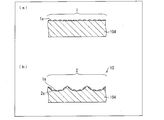
- (A) is sectional drawing which shows typically the structure in the initial stage of manufacture of the reflection preventing structure of this invention
- (b) is sectional drawing which shows typically the cross section of the reflection preventing structure of this invention.
- It is the schematic shows the example of a change of the said reflection preventing structure manufacturing apparatus.
- It is the schematic which shows another modification of the said reflection preventing structure manufacturing apparatus It is the schematic which shows the structure of the reflection preventing structure manufacturing apparatus which concerns on other embodiment of this invention.
- FIG. 1 It is the schematic which shows the structure of the reflection preventing structure manufacturing apparatus which concerns on another embodiment of this invention.
- (A)-(e) is sectional drawing which shows each process of the reflection preventing structure manufacturing method which concerns on other embodiment of this invention.
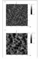
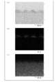
- (A) is a figure which shows the AFM image which observed the surface of the 1st convex structure of the antireflection structure manufactured in one Example of this invention in the scanning range of 1 micrometer square
- (b) is 2nd It is a figure which shows the AFM image which observed the surface of the concave structure in the scanning range of 1 micrometer square.
- (A) is a figure which shows the spectrum which carried out the two-dimensional Fourier transform of the AFM measurement result of the 1st convex structure in the said Example
- (b) is a figure which shows power spectral density.
- (A) is a figure which shows the cross-sectional transmission electron microscope image of the 1st convex structure in the said Example
- (b) is a figure which shows the EDX mapping image about Ta
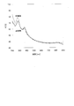
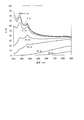
- (c) is the EDX mapping about Si. It is a figure which shows an image. It is the graph which showed the measurement result of the reflectance in the antireflection structure manufactured in the said example together with the measurement result of a comparative sample and a reference sample.
- mainly or “mainly comprising” means that the component is contained in the largest amount among all components, and preferably 50% by mass or more of the component is contained. Most preferably, the component is contained in an amount of 100% by mass. Further, “A to B” indicating a range means that it is A or more and B or less.
- FIG. 1A is a cross-sectional view schematically showing the structure of the antireflection structure of the present invention in the initial production stage
- FIG. 1B is a cross-sectional view schematically showing the cross section of the antireflection structure 10. is there.
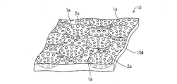
- FIG. 2 is a perspective view schematically showing the structure of the antireflection structure 10. Note that FIG. 2 is a diagram in which the structure of the antireflection structure 10 is extremely deformed for easy understanding. For the actual structure, refer to FIGS. 10A and 10B described later. I want to be.
- the antireflection structure 10 prevents reflection of light, and has a plurality of concave portions 2 a (a plurality of convex portions 1 a (small convex portions) on its surface.
- a large concave portion is formed on the surface of the base body 104.
- the 1st convex structure 1 is comprised by the some convex part 1a
- the 2nd concave structure 2 is comprised by the some recessed part 2a.
- the plurality of recesses 2 a are not necessarily formed densely on the surface of the base body 104. That is, the concave portion 2 a is not formed, and a portion where only the convex portion 1 a is formed may exist on the surface of the base body 104. However, in order to enhance the antireflection effect, it is preferable that the recesses 2 a are formed densely on the surface of the base body 104.
- the substrate 104 may be an optical element for forming the antireflection structure, or may be a transfer master for transferring and forming the antireflection structure on the surface of the optical element.
- the antireflection structure 10 is the optical element itself. However, the antireflection structure 10 and the optical element may be formed separately.
- the pitch between the plurality of protrusions 1a (distance between the vertices of the protrusions) and the pitch between the recesses 2a (distance between the centers of the recesses) are the wavelengths of light incident on the antireflection structure 10 (or Smaller than the wavelength of light emitted from the antireflection structure 10. Therefore, the width (caliber) of the concave portion 2a is necessarily larger than the width of the convex portion 1a (the width in the direction along the surface of the substrate 104) and smaller than the wavelength of the light.
- the average pitch between the recesses 2a is, for example, 1.2 times or more and 10 times or less than the average pitch between the projections 1a.
- the average pitch between the convex parts 1a is 7 nm or more and 40 nm or less, for example, and the average pitch between the concave parts 2a is 28 nm or more and 250 nm or less.
- a structure formed when an antireflection structure including the convex portion 1a and the concave portion 2a is transferred to another substrate is also included in the technical scope of the present invention.
- the presence of the plurality of recesses 2a on the surface of the substrate 104 at a pitch smaller than the wavelength of incident light results in the formation of large irregularities that are smaller than the wavelength of the incident light. Acts as a structure.
- the presence of the plurality of convex portions 1a on the surface of the concave portion 2a at a pitch smaller than the wavelength of the incident light results in the formation of small irregularities smaller than the wavelength of the incident light. Also functions as a moth-eye structure.
- the antireflection structure 10 has two types of moth-eye structures, a moth-eye structure formed by the first convex structure 1 and a moth-eye structure formed by the second concave structure 2.
- the antireflection effect can be enhanced as compared with the conventional configuration in which a single moth-eye structure is formed.
- Patent Document 3 has a structure (macro structure) larger than the wavelength of incident light and a structure (micro structure) smaller than the wavelength of the incident light. It does not correspond to structure 2. This is because the pitch between the recesses 2a is smaller than the wavelength of light incident on the antireflection structure 10, but the size of the macro structure is larger than the wavelength of incident light. Therefore, the invention of Patent Document 3 is essentially different from the present invention.
- the body 10 can be manufactured.
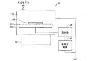
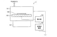
- the antireflection structure manufacturing apparatus 11 includes a vacuum chamber 101, a base support member 102 that supports the base 104, a supply source 103 that supplies a supply material to the base 104, a high-frequency power source 105, a matching unit 106, A vacuum pump 107 is provided.
- the antireflection structure manufacturing apparatus 11 performs a sputter etching process on the base body 104 and supplies a supply material from the supply source 103 to the base body 104, whereby the first convex structure 1 and the surface of the base body 104 are provided.
- the antireflection structure 10 having the second concave structure 2 is formed.
- the base 104, the base support member 102, and the supply source 103 are provided in the vacuum chamber 101.
- a vacuum pump 107 is connected to the vacuum chamber 101 so that the inside of the vacuum chamber 101 can be in a reduced pressure state.
- a gas pipe for introducing an inert gas typified by Ar, Kr, or Xe into the vacuum chamber 101 is connected.
- plasma discharge is generated in the vacuum chamber 101 by introducing the above inert gas and applying a high frequency voltage, and the antireflection structure 10 is formed on the substrate 104 using a sputtering phenomenon. It becomes possible to form.
- a supply source 103 is formed on the surface of the substrate support member 102, and a substrate 104 is attached on the supply source 103. Therefore, the substrate support member 102 supports the supply source 103 and the substrate 104.
- a high frequency power source 105 is electrically connected to the base support member 102. Therefore, it is desirable that the substrate support member 102 be formed using a metal material having good conductivity.
- the configuration of the base support member 102 is not particularly limited as long as it can support the base 104.
- a configuration in which the base 104 is fixed with a screw or a spring, a configuration in which the base 104 is fixed using a magnet, a configuration in which vacuum suction is performed, and the like can be used. .
- the substrate support member 102 may be a member that rotates in the vacuum chamber 101, or a member that is supplied with power from the high-frequency power source 105 and a member that supports the element.
- a portion of the substrate support member 102 that supports the substrate 104 may be directly electrically connected, or may be indirectly electrically connected through another member.
- the base body support member 102 may be formed by combining a rotating body and a pedestal, holding the base body 104 on the rotating body, and supplying power from the high-frequency power source 105 to the pedestal.
- the supply source 103 supplies a supply material to the surface of the base body 104 in order to form the antireflection structure 10.
- This feed material forms particles by being mixed with a base material constituting the surface of the base 104 (hereinafter simply referred to as base material) released as molecules or atoms, and more preferably the base material. It forms particles of materials and compounds.
- the supply source 103 supplies the supply material from the supply source 103 in the form of atoms or molecules (hereinafter sometimes abbreviated as “atoms etc.”) to the surface of the substrate 104.
- the supply material in the state of atoms or the like is capable of forming fine particles (convex portions 1a) on the surface of the base 104, and more preferably, a material and a compound on the surface of the base 104 are generated and formed on the surface of the base 104. It is possible to form fine particles of the compound.
- a state transition diagram (Phase Diagram) can be used.
- the “feed material capable of generating a base material and a compound” in the present specification means a feed material having a compound region with the base material in a state transition diagram with the base material. More preferably, it means a feed material having a region of a compound with the base material in the fine particle formation conditions (temperature, pressure) used in the state transition diagram with the base material.
- the material used for the supply source 103 is not particularly limited when a substrate material and a supply material capable of generating a compound are selected.
- a material mainly composed of a transition metal element can be selected. More specifically, high melting point transition metal materials V, Cr, Fe, Zr, Nb, Mo, Tc, Ru, Rh, Pd, Hf, Ta, W, Re, Os, Ir, and Pt
- the convex portion 1a includes any one of V, Cr, Fe, Zr, Nb, Mo, Tc, Ru, Rh, Pd, Hf, Ta, W, Re, Os, Ir, or Pt. Become.
- This feed material is fed at a very low rate so that it is not formed as a continuous film on the substrate 104 during the process.
- the supply source 103 is disposed at a position where the supply material cannot directly enter the surface of the base body 104.
- the “position where the supply material cannot be directly incident” in the present specification is realized by, for example, arranging the base body 104 at a position where the supply material emitted from the supply source 103 does not reach linearly. be able to. Further, as will be described later, a shield is provided between the surface of the base 104 and the supply source 103 that supplies the supply material so that the supply material cannot go straight from the supply source 103 to reach the surface of the base 104. It may be realized.
- the supply source 103 may be formed as a thin film on the substrate support member 102 or may be formed in a bulk shape.
- the supply source 103 does not need to be formed on the entire surface of the substrate support member 102, and may be formed at least in a region other than the region hidden by the substrate 104.
- the thickness of the supply source 103 is not lost in the sputter etching process in which the antireflection structure 10 including the first convex structure 1 and the second concave structure 2 is formed. Form with.
- a material is selected in which the supply material supplied from the supply source 103 exhibits poor wettability on the surface of the substrate 104 and can generate fine particles on the substrate 104. More preferably, a compound such as atoms and the like supplied from the supply source 103 is preferably generated.
- a semiconductor material mainly containing an element typified by Si or Ge, or Al can be used.
- the base material 104 is not particularly limited as long as these materials are formed on the surface thereof. Therefore, in addition to the above materials, for example, SiO 2 or Al 2 O 3 , an insulator material typified by glass, a semiconductor material typified by GaAs or GaN, various metal materials, etc. In addition, a resin substrate can be used.
- the fine particles generated when the supply material supplied from the supply source 103 forms the fine particles that become the convex portions 1 a on the base 104 It is further desirable to select materials so that the wettability is poor with respect to the surface of the substrate 104.
- the prevention structure 10 can be provided.
- the periodicity of the 1st convex structure 1 is high means that the space
- the high periodicity of the second concave structure 2 means that the interval at which the concave portions 2a are formed (the pitch between the plural concave portions 2a) is within a predetermined range.
- the surface energy on the substrate 104 side is reduced, the surface energy on the particle side and the substrate 104 are reduced. It is important to increase the interfacial energy between the particles and the fine particles. Therefore, it is desirable to use a material having a large surface energy as the material of the supply source 103 and to use a material having a small surface energy as the base material.
- the base material is preferably a material having a lower melting point than the material used for the supply source 103.
- the base material and the supply material are selected so that the supply material supplied from the supply source 103 generates the base material and the compound fine particles on the base 104, the supply material does not generate the base material and the compound. Compared with the fine particles to be formed, the melting point of the obtained fine particles can be lowered (when the melting point of the base material is lower than the supply material). As a result, the fine particles formed on the substrate 104 have such a property that they are not compatible with the surface of the substrate 104, and the particles are grown to such an extent that they can be applied as the convex portions 1a necessary for forming the antireflection structure 10. be able to.
- a high melting point material that forms extremely small particles of about 1 to 2 nm or less on the substrate 104 when a material that cannot generate a compound with a supply material is used as the substrate material. Even so, by making the base material a material capable of generating a compound with the feed material, the melting point of the resulting fine particles (compound) is lower than the melting point of the feed material, and the fine particles are deposited on the base 104. Can grow to particles having a diameter of about 4 nm to several tens of nm.
- the high frequency power source 105 applies a high frequency voltage having positive and negative polar components to at least one of the base body 104 and the base body supporting member 102.
- the high-frequency power source 105 is electrically connected to the base member 102 via a matching unit 106 that adjusts impedance.
- the high-frequency power source 105 is a power source that generates a high-frequency voltage in a frequency range in which the supply material can be knocked out from the supply source 103 by sputtering, specifically, a range of 100 kHz to 100 MHz, A high-frequency voltage having both positive and negative components can be supplied.
- a power source that generates a high-frequency voltage in the vicinity of 13.56 MHz which is a general power source for high-frequency sputtering, can be used.
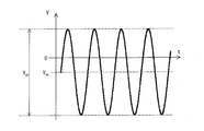
- FIG. 4 shows an example of a high-frequency voltage waveform having both positive and negative components.
- the high-frequency voltage generated by the high-frequency power source 105 has, for example, a substantially sine wave shape, and both positive and negative components with respect to the ground voltage (0 line in FIG. 4). have.
- Vpp the difference between the maximum value and the minimum value of the high frequency voltage
- Vdc the value obtained by subtracting the ground voltage from the average value of the high frequency voltage
- Vdc is applied in the negative direction as shown in FIG. 4, in other words, in the direction in which the surface of the substrate 104 is sputter-etched.
- vacuum pump 107 Any pump can be used as the vacuum pump 107 as long as the vacuum chamber 101 can be in a reduced pressure state.
- a rotary pump or a dry pump, a turbo molecular pump, a cryopump, and a diffusion pump are used. Any pump selected from pumps can be used in combination.
- the side opposite to the substrate support member 102 side of the high-frequency power source 105 is in a grounded state and is shown as having the same potential as the wall surface of the vacuum chamber 101.
- Any structure can be used as long as it can be applied, and is not limited to such a configuration.
- a counter electrode may be disposed in the vacuum chamber 101 and may have the same potential as that of the high frequency power source 105 on the side opposite to the substrate support member 102 side.
- a sputtering apparatus capable of sputter etching may be applied to the antireflection structure manufacturing apparatus in the present application.
- the vacuum chamber 101 is evacuated using the vacuum pump 107, and the vacuum chamber 101 is depressurized.
- the ultimate vacuum at this time is not particularly limited, but from the viewpoint of reducing the influence of contaminants, for example, it is set to 1 ⁇ 10 ⁇ 3 Pa or less, more desirably 1 ⁇ 10 ⁇ 4 Pa or less.
- an inert gas is introduced from the gas pipe.
- the pressure (gas pressure) inside the vacuum chamber 101 is, for example, about 1 ⁇ 10 ⁇ 2 Pa to 1 Pa.
- first convex structure 1 Formation of first convex structure 1> Subsequently, the high frequency power source 105 is energized, and a high frequency voltage is applied to the substrate support member 102. At this time, plasma discharge occurs due to the introduction of the inert gas into the vacuum chamber 101, and sputtering occurs.
- Vpp The difference between the maximum value and the minimum value of the high frequency voltage at this time is set to 200 V to 2000 V, for example.
- a value (Vdc) obtained by subtracting the ground voltage from the average value of the high-frequency voltage is, for example, ⁇ 500 V to 0 V.
- the relationship between Vpp and Vdc is set so that Vpp is larger than the absolute value of Vdc.
- the high frequency voltage has both positive and negative components with respect to the ground voltage.
- the order of introducing the inert gas and applying the high-frequency voltage may be reversed.
- Vdc a negative value
- sputtering sputter etching
- the magnitude of the high-frequency voltage may be controlled by the incident power and the reflected power with respect to the substrate support member 102.
- the incident power is set such that the incident power per unit area divided by the area of the substrate 104 mounting surface of the substrate support member 102 the incident power, the example 0.02W / cm 2 ⁇ 1.2W / cm 2 of about To do.
- the reflected power is desirably as small as possible, but is, for example, about 10% or less of the incident power.
- the kinetic energy in the direction of colliding with the substrate support member 102 with respect to the inert gas ions in the vacuum chamber 101 is increased.
- the substrate material constituting the substrate 104 is released as molecules or atoms, and a supply material that forms particles by being mixed with the substrate material is supplied from the supply source 103. (Supply process).
- a plurality of convex portions 1a are formed on the surface of the base body 104 by mixing the base material released in the supply step and the supplied supply material (convex portion forming step). At this time, the convex portions 1 a are formed at a pitch smaller than the wavelength of light incident on the antireflection structure 10.
- the first convex structure 1 formed by periodically forming the convex portions 1a is formed on the base body 104 while forming a gap between the particles. It is formed.
- the time for forming the first convex structure 1 is not particularly limited, but may be, for example, in the range of about 100 seconds to 1 hour.
- Second concave structure 2 After the first convex structure 1 is formed, the same high frequency voltage as that for forming the first convex structure 1 is applied to cause sputtering, and the supply material is continuously supplied to the surface of the substrate 104 and sputtered. By performing the etching process, the second concave structure 2 generated due to the existence of the first convex structure 1 on the base body 104 is formed on the surface of the base body 104.
- the plurality of concave portions 2a having the convex portions 1a on the surface are formed on the surface of the substrate 104 at a pitch smaller than the wavelength of incident light.
- the average period (7 nm to 40 nm) of the convex portion 1 a is the light incident on the antireflection structure 10. It can be said that it is smaller than the wavelength.
- the average period of the second concave structure 2 The size of the concave part 2a varies depending on the supply material, the material of the surface of the base 104, and the conditions for applying a high-frequency voltage. Compared to the first convex structure 1, it is formed with an average period of about 1.2 to 10 times, and the height (depth) of the concave portion 2a is about 1.5 to 20 times the height of the convex portion 1a. It is formed.
- the second concave structure 2 can be formed with an average period of about 28 nm to 250 nm.
- the height of the first convex structure 1 having the first period is about 5 nm
- the height (depth) of the second concave structure 2 can be formed with a size of about 7 nm to 100 nm. Due to the presence of the second concave structure 2, the antireflection structure 10 having a high antireflection effect can be formed on the base body 104, particularly at a wavelength from blue to ultraviolet light.
- the supply material supplied from the supply source 103 may be supplied at a rate that is low enough not to be formed as a continuous thin film on the substrate 104. Although it does not limit, it discharge
- the supply atoms and the like emitted from the supply source 103 are obstructed by the base body 104 itself and directly form the first convex structure 1 and the second concave structure 2 in the base body 104. It does not enter the surface to be formed.
- the antireflection structure forming process of the present embodiment is a process in which negative Vdc is applied to the substrate 104, that is, a sputter etching process.
- a sputter etching process When the sputter etching process is performed in the apparatus configured as shown in FIG. 3, plasma that causes sputtering is generated by a high frequency voltage applied between the substrate support member 102 and the chamber wall, and the surface of the substrate 104 is etched.
- the surface of the substrate 104 is subjected to sputter etching in a normal sputter etching process in which the first convex structure 1 does not exist. Along with this, smoothing proceeds.
- Non-Patent Document 1 discloses a ripple shape formed on a Si substrate when the Si substrate is mounted in an ion beam sputtering apparatus and Ar ions are irradiated from an oblique direction with respect to the substrate surface. ing.
- Non-Patent Document 1 since the inert gas ions are irradiated to the substrate from the ion gun, the sputtering is performed only from one direction with respect to the substrate. According to Non-Patent Document 1, when the inert gas ions are incident on the substrate from a certain incident angle and the Si substrate is etched, a ripple shape is formed on the substrate.
- sputter etching (second concave structure forming step) is subsequently performed on the base body 104 in a state where the first convex structure 1 is formed, and during the second concave structure 2 forming step, However, the elements constituting the convex portion 1a are continuously supplied so that the first convex structure 1 is maintained.
- the inert gas ions having a component with a small incident angle are prevented from reaching the surface of the substrate 104 on the back side due to the presence of the convex portion 1a because of being blocked by the first convex structure 1.
- the symmetry at the time of sputter etching is lost, ripples are not canceled out, and sputter etching progresses particularly at locations where the etching strength is increased by the overlapping (interference) of the ripples. It is thought that it is growing.
- the first convex structure 1 is densely formed with an interval of several tens of nanometers or less, and (Ii) It is considered that it is important that the supply material is continuously supplied to the surface of the substrate 104 during the sputter etching for forming the second concave structure 2.
- the first convex structure 1 formed in the first step is replaced with the second concave structure 2 in the subsequent second step. Even at the stage where the is formed, it remains on the surface.
- the first convex structure 1 does not necessarily have a clear periodicity, and the first convex structure 1 may be formed at a high density with an interval of several nanometers to several tens of nanometers. It ’s fine. However, from the viewpoint of forming the second concave structure 2 having a more uniform shape and period, it is particularly desirable to have a high periodicity.
- the first convex structure 1 is first formed, and then the second concave structure generated by the presence of the first convex structure 1.
- the antireflection structure 10 is obtained by forming the first and second convex structures 1 and the second concave structure 2 by continuously performing a substantially single process. It is possible.
- the antireflection structure 10 can be manufactured by a single process. Furthermore, since it can be manufactured using only a dry process in a vacuum apparatus, it is possible to prevent the substrate 104 from being contaminated and to form the antireflection structure 10 without deteriorating the characteristics of the substrate 104.
- the substrate 104 whose surface is composed of a material that forms a compound with a high melting point transition metal represented by Si or Ge, the substrate 104 needs to be specially treated.
- the antireflection structure 10 can be directly formed. Therefore, it is particularly suitable for directly forming the antireflection structure 10 on the optical element made of these materials.
- the antireflection structure 10 can be formed on the surface of the substrate 104 of a low melting point material typified by plastic. Further, since the gas to be supplied is an inert gas, there is no possibility that the gas reacts with the substrate 104 and deteriorates.
- the antireflection structure 10 is formed using sputter etching, it can be formed even if the surface of the substrate 104 is a curved surface.
- Patent Document 4 discloses a method of forming fine particles corresponding to the convex portion 1a.
- the present invention extends the time of the fine particle formation step (fine particle formation step) or increases the high-frequency voltage applied to the substrate support member 102 during fine particle formation.
- the recess 2a is further formed.
- Prolonging the time of the fine particle forming step is generally not preferable because it increases the time of the manufacturing process, and therefore, an attempt to extend the time of the fine particle forming step has not been conventionally performed. Accordingly, it has been difficult for those skilled in the art to find that the concave portion 2a is formed if the fine particle forming step is extended.
- the manufacturing cost increases if the high-frequency voltage applied to the substrate support member 102 is increased, it is preferable to form the convex portion 1a with as little power consumption as possible. Therefore, in a situation where a range of applied voltages in which the convex portions 1a can be sufficiently formed has been found, no attempt has been made in the past to apply an applied voltage exceeding that range. Therefore, it has been difficult for those skilled in the art to find that the concave portion 2a is formed if the applied voltage in the fine particle forming step is increased.
- the present invention has been conceived as a result of breaking such a fixed idea and extending the time of the formation process of the convex part 1a or increasing the applied voltage in the formation process of the convex part 1a. This cannot be easily conceived from Patent Document 4.
- the base body 104 and the base body support member 102 may or may not be electrically connected. Even when the substrate 104 is not electrically conductive, the substrate support member 102 exists in the immediate vicinity of the substrate 104, so that ions given kinetic energy toward the substrate support member 102 reach the substrate 104. For this reason, the same effect as the case where it is conducting can be obtained.
- a first material having high periodicity is used even when a non-conductive base material is used as the substrate 104 and a material that forms a compound that generates atoms and compounds supplied from the supply source 103 is used on the surface.
- the convex structure 1 is obtained.
- the high frequency voltage may be directly applied to the base body 104 without using the base body support member 102.
- the material constituting the supply source 103 (the supply material supplied from the supply source 103) can form fine particles on the surface of the base 104, in other words, the supply material and the base material. Is a combination that results in poor wettability, more preferably a combination that forms a compound, and (ii) that a high-frequency voltage is applied to the substrate 104, particularly preferably.
- the arrangement of the base 104 and the supply source 103 is such that atoms or the like supplied from the supply source 103 to the base 104 do not directly enter the base 104.
- the present invention is not limited to the apparatus configuration shown in FIG. 3 as long as the apparatus configuration satisfies the elements including (i) and (ii), more preferably (iii). is not.
- the substrate support member 102 itself may be a supply source.
- the supply source 103 may serve as a base support member.
- the supply source 103 may be arranged at a position adjacent to the base support member 102 as a member different from the base support member 102.
- 5 and 6 are schematic views showing a modification of the antireflection structure manufacturing apparatus.
- the power source that supplies voltage (power) to the supply source 103 and the power source that supplies voltage (power) to the base body 104 may be separate power sources.
- the power source for supplying voltage (power) to the supply source 103 may be a DC power source instead of a high frequency power source. 3, 5, and 6, the high-frequency voltage may be applied to the substrate support member 102 to the substrate 104.
- the supply source 103 is not supplied with power from the high-frequency power source 105, but is supplied with atoms or the like from the supply source 103 by irradiating the supply source 103 with an ion beam or electron beam.
- An ion source or an electron source may be provided.
- a heating source for heating the supply source 103 to evaporate the molecules may be provided.
- the supply source 103 is arranged on the front side of the substrate 104 (upward on the paper surface in FIGS. 3, 5 and 6), sputtering is performed between the supply source 103 and the substrate 104 when a high frequency voltage is applied.
- the potential difference is not generated such that the potential difference between the base 104 and the supply source 103 is the same as the arrangement of the base 104 and the supply source 103 described in the above (iii).
- the arrangement is such that the first convex structure 1 and the second concave structure 2 can be more preferably formed.
- FIG. 7 is a cross-sectional view showing a schematic configuration of the antireflection structure manufacturing apparatus 21 according to the present embodiment.
- the antireflection structure manufacturing apparatus 21 is similar to the antireflection structure manufacturing apparatus 11 described in Embodiment 1, and includes a vacuum chamber 101 and a substrate support provided inside the vacuum chamber 101.
- the member 102, the base 104 attached to the base support member 102, the high frequency power source 105 that applies a high frequency voltage to the base support member 102, the matching unit 106 that adjusts the impedance, and the vacuum chamber 101 are evacuated. And a vacuum pump 107.
- a supply source 203 that supplies atoms and the like to the substrate 104 is disposed as a sputtering target material, and is common to the high-frequency power source 105 that applies a high-frequency voltage to the substrate support member 102 or a high-frequency signal.
- a sputtering power supply different from the power supply 105 is connected, and atoms and the like are emitted from the supply source 203 by sputtering.
- the material constituting the supply source 203 is the same as that of the supply source 103 described above.
- (B) Shield member 208 In addition, in the present embodiment, a shielding member 208 for preventing atoms and the like from the supply source 203 from directly entering the substrate 104 is disposed on a straight line connecting the supply source 203 and the substrate 104.
- the material constituting the shielding member 208 is not particularly limited as long as atoms and the like supplied from the supply source 203 can be shielded, but it is preferable to use a member that can withstand damage caused by sputtering.
- a member that can withstand damage caused by sputtering For example, stainless steel, aluminum, aluminum alloy, glass, or the like can be used.
- the shielding member 208 is set to the ground voltage or the same potential as the substrate supporting member 102 so that the shielding member 208 is sputtered and the material constituting the shielding member 208 does not adhere to the substrate 104.
- the shielding member 208 By arranging the shielding member 208 in this way, atoms and the like emitted from the supply source 203 cannot directly reach the substrate 104 in a straight line, and the inert gas or supply that exists in the film formation atmosphere is not possible. Atoms scattered by colliding with other atoms emitted from the source 203, atoms having low energy colliding with the shielding member 208 and scattered or diffracted reach the surface of the substrate 104.
- the supply material supplied from the supply source 203 is a material having a higher melting point than the material constituting the surface of the substrate 104
- the particles grown on the substrate 104 are wet with respect to the surface of the substrate 104.
- isolated fine particles having periodicity are formed on the substrate 104 while forming a gap between the particles.
- the first convex structure 1 having a high periodicity on the order of nanometers can be formed.
- a high-frequency voltage is continuously applied to cause the same sputtering as in the case of forming the first convex structure 1, and the supply material is continuously supplied to the surface of the substrate 104 and the sputter etching process is performed.
- a second concave structure 2 is generated on the surface of the base 104 due to the presence of the convex structure 1 on the base 104.
- the sputtering power supplies to supply 203, for example, per unit area, and 0.2W / cm 2 ⁇ 8.2W / cm 2 approximately.
- a sputtering target having a diameter of 6 inches is used as the sputtering source of the supply source 203, it corresponds to applying power of about 30 W to 1.5 kW.
- the difference (Vpp) between the maximum value and the minimum value of the high-frequency voltage applied to the substrate support member 102 is set to 200 V to 2000 V, for example, as in the first embodiment.
- the value (Vdc) obtained by subtracting the ground voltage from the average value of the high-frequency voltage is set to, for example, ⁇ 500 V to 0 V.
- the relationship between Vpp and Vdc is set so that Vpp is larger than the absolute value of Vdc.
- the high frequency voltage has both positive and negative components with respect to the ground voltage. Further, by setting Vdc to a negative value, sputtering (sputter etching) is performed in a direction in which the surface of the substrate 104 is etched in the entire process.
- the magnitude of the high-frequency voltage may be controlled by the magnitude of the incident power and the reflected power with respect to the base support member 102.
- the incident power per unit area obtained by dividing the incident power by the area of the base 104 attachment surface of the base support member 102 is, for example, 0.02 W / set to be cm 2 ⁇ 1.2W / cm 2 about.
- the reflected power is desirably as small as possible, but is, for example, about 10% or less of the incident power.
- the surface of the substrate support member 102 is protected by a hardly sputtered material, or the same material as the supply source 203 is formed on the surface of the substrate support member 102 as in the first embodiment. It is desirable that Alternatively, the base support member 102 itself may be the same material as the supply source 203.
- the substrate support member 102 may be made as small as the substrate 104 so that the constituent material of the substrate support member 102 does not reach the surface of the substrate 104.
- the presence of the shielding member 208 makes it possible to form the first convex structure 1 and the second concave structure 2 of the base body 104 (on the upper side of the base body 104 shown in FIG. 7). ),
- the supply atoms emitted from the supply source 203 are not directly incident (arrangement where the supply atoms are prevented from linearly entering the surface on which the fine particles are formed)) Since the supply atoms can be easily prevented from being formed as a continuous thin film on the substrate 104, the arrangement is more preferable.
- the supply source 203 is not supplied with power from the sputtering power source, but is irradiated with an ion beam or an electron beam from the supply source 203.
- An ion source or an electron source for supplying atoms or the like may be provided.
- a heating source for heating the supply source 203 to evaporate the molecules may be provided.
- the first convex structure 1 (fine particles) is produced on the surface of the base 104, and then the second antireflection structure manufacturing apparatus 21 is used. If the method for producing the concave structure 2 is used, the magnitude of the high-frequency voltage (Vpp and Vdc) applied to the substrate 104 and the sputtering power supplied to the supply source 203 can be individually adjusted. The degree of freedom to control the height and periodicity of the antireflection structure is increased.
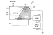
- FIG. 8 is a cross-sectional view showing a schematic configuration of the antireflection structure manufacturing apparatus 31 according to the present embodiment.
- the antireflection structure manufacturing apparatus 31 is provided inside the vacuum chamber 101 and the vacuum chamber 101, similarly to the antireflection structure manufacturing apparatuses 11 and 21 shown in the first and second embodiments.
- the antireflection structure manufacturing apparatus 31 is provided with a supply source 203 for supplying atoms and the like to the base 104 as a sputtering target material.
- a sputtering power supply that is common to the high-frequency power supply 105 for applying a high-frequency voltage or different from the high-frequency power supply 105 is connected, and atoms and the like are emitted from the supply source 203 by sputtering.
- the substrate 104 is arranged at a position outside the emission range of the discharge plasma 309 such as atoms emitted from the supply source 203. Yes.
- the range of the discharge plasma 309 can be generally discriminated by visually observing the discharge state when the supply source 203 is sputtered, but confirming the range where high periodicity can be obtained while changing the position of the substrate 104 little by little. Is more preferable.
- a straight line connecting an end portion of the supply source 203 closest to the base 104 and an end portion of the base 104 closest to the supply source 203 and a surface of the supply source 203 (plasma).
- the antireflection structure of the present embodiment can also be produced by setting ⁇ to be approximately 55 degrees or less, where ⁇ is the angle formed with the extension line of the surface of the base body 104 side where the light is generated. .
- a member called an earth shield surrounds the target material.
- the ground shield when a part of the discharge plasma is shielded by the ground shield (that is, when the substrate 104 is surrounded by the ground shield), the ground shield is In order to function as a shielding member, in the area corresponding to the shaded shaded portion, as shown in the second embodiment, the highly periodic fine particles (first convex structure 1), and the second caused by this, A concave structure 2 is obtained.
- the supply material supplied from the supply source 103 may be supplied at a rate that is low enough not to be formed as a continuous thin film on the substrate 104, and the supply method is not limited.
- the supply material discharged from the supply source 203 is directly applied to the surface of the substrate 104 on which fine particles are to be formed (the upper surface of the substrate 104 shown in FIG. 8).
- the arrangement is such that it does not enter (the arrangement in which the supply material does not enter linearly), and the supply atoms can be easily prevented from being formed as a continuous thin film on the substrate 104, which is a more preferable arrangement.
- the high frequency voltage applied to the base support member 102 causes the surface of the base 104 to be repeatedly knocked out and attached, thereby causing the base Particles grow while fine particles containing atoms and the like supplied from the supply source 203 are generated on the surface 104, and the first convex structure 1 is formed.
- the supply material supplied from the supply source 203 is a material having a higher melting point than the base material constituting the surface of the base 104
- the particles grown on the base 104 are thus, the wettability is poor, and the particles are formed as isolated fine particles having periodicity on the substrate 104 while forming a gap between the particles.
- the first convex structure 1 having a high periodicity on the order of nanometers can be formed.
- a high-frequency voltage is continuously applied to cause the same sputtering as in the case of forming the first convex structure 1, and the supply material is continuously supplied to the surface of the substrate 104 and the sputter etching process is performed.
- a second concave structure 2 is formed on the surface of the base 104 due to the presence of the convex structure 1 on the base 104.
- the sputtering power supplies to supply 203, and 2 ⁇ 5.5W / cm 2 approximately per unit area for example 0.05 W / cm.
- a sputtering target having a diameter of 6 inches is used as the sputtering target of the supply source 203, it corresponds to applying electric power of about 10 W to 1 kW.
- the difference (Vpp) between the maximum value and the minimum value of the high-frequency voltage applied to the substrate support member 102 is set to 200 V to 2000 V, for example, as in the first and second embodiments.
- the value (Vdc) obtained by subtracting the ground voltage from the average value of the high-frequency voltage is set to, for example, ⁇ 500 V to 0 V, as in the first and second embodiments.
- the relationship between Vpp and Vdc is set so that Vpp is larger than the absolute value of Vdc.
- the high-frequency voltage has both positive and negative components with respect to the ground voltage.
- Vdc sputtering (sputter etching) is performed in a direction in which the surface of the substrate 104 is etched in the entire process.
- the magnitude of the high-frequency voltage may be controlled by the magnitude of the incident power and the reflected power with respect to the base support member 102.
- the incident power per unit area obtained by dividing the incident power by the area of the mounting surface on the base body 104 of the base body supporting member 102 is, for example, as in the first and second embodiments. , set to be 0.02W / cm 2 ⁇ 1.2W / cm 2 approximately.
- the reflected power is desirably as small as possible. For example, it is about 10% or less of the incident power.
- the supply material (atom or the like) released from the supply source 203 collides with an inert gas molecule such as Ar or the supply material (atom or the like) existing in the sputtering atmosphere and leaves the supply source 203. Since the energy is gradually lost, even when the substrate 104 is arranged by removing the discharge plasma 309 in the direction away from the supply source 203, the case where the substrate 104 is arranged by removing the discharge plasma 309 in the lateral direction of the supply source 203 The same effect can be obtained.
- the distance between the supply source 203 and the substrate 104 is emitted from the supply source 203. It is desirable that the average free path of the supplied material (atoms etc.) is about twice or more.
- the substrate support member 102 does not necessarily need to be disposed outside the range of the discharge plasma 309, and at least the substrate 104 may be disposed outside the region of the discharge plasma 309.
- the supply source 203 is not supplied with power from the sputtering power supply, and the supply source 203 is irradiated with an ion beam or an electron beam to supply atoms and the like from the supply source 203.
- An ion source or an electron source may be provided.
- a heating source for heating the supply source 303 to evaporate the molecules may be provided.
- FIG. 9 is a schematic view showing a method for manufacturing an antireflection structure according to this embodiment.
- the antireflection structure 41 is obtained by forming the first convex structure 1 and the second concave structure 2 on the surface of the base 104 in the manufacturing method shown in the first to third embodiments, and using the first convex structure 1 and the second concave structure 2 as a master.
- the structure is transferred to the second substrate (substrate) 404 using a transfer method represented by a known nanoimprint method or injection molding method, and an antireflection structure is formed on the second substrate 404.
- An antireflection structure 42 is obtained by further transferring the antireflection structure 41.
- the height of the concavo-convex structure on the second substrate 404 may be increased so that a greater antireflection effect can be obtained.
- the second base 404 may be an optical element that is intended to form an antireflection structure.
- the material constituting the second base 404 is not particularly limited. For example, SiO 2 or Al 2 O 3 , an insulator material typified by glass, a semiconductor typified by Si, Ge, GaAs, or GaN. Materials, various metal materials, and resin substrates can be used.
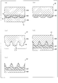
- FIG. 9 is a cross-sectional view showing a cross section of the antireflection structure in each step included in the manufacturing method of the antireflection structure according to the present embodiment.
- the convex portion 1a and the concave portion 2a are formed on the substrate 104 by using the same manufacturing method as that shown in the first to third embodiments.
- a second substrate 404 having a transfer layer 405 typified by a nanoimprint resin formed on one surface is prepared, and the transfer layer 405 has an uneven structure of the substrate 104.
- the uneven structure of the base body 104 is transferred to the transfer layer 405 by pressing against the formed surface.
- the pressing at the time of transfer is performed by applying a pressure of about 0.1 MPa to 10 MPa, and heating or ultraviolet light irradiation is performed as necessary to soften or harden the transfer layer 405. Further, a release agent for facilitating peeling after transfer (peeling between the second substrate 404 and the transfer layer 405) may be applied on the transfer layer 405.
- anisotropic etching is performed on the second substrate 404 from the transfer layer 405 side, and the concavo-convex structure corresponding to the concavo-convex structure of the transfer layer 405 is formed on the second substrate. 404 is formed.
- the difference between the two etching rates is used as shown in FIG. 9C. It is possible to transfer and form on the second substrate 404 while enhancing the height of the uneven structure.
- the anisotropic etching treatment may be performed by, for example, a RIE (Reactive Ion Etching) method in which plasma is generated in a state where a halogen-based reactive gas typified by fluoride or chloride is introduced, and anisotropic etching is performed. It is possible to apply an isotropic wet etching method.
- RIE Reactive Ion Etching
- the unevenness of the antireflection structure formed on the second substrate 404 is reversed from the unevenness formed on the substrate 104. That is, a plurality of convex portions (large convex portions) 4a having concave portions (small concave portions) 3a on the surface are formed on the surface of the second base 404 at a pitch smaller than the wavelength of incident light.
- the average pitch between the plurality of convex portions 4a is, for example, 1.2 times to 10 times the average pitch between the plurality of concave portions 3a, and the average pitch between the plurality of concave portions 3a is, for example,
- the average pitch between the plurality of convex portions 4a is, for example, not less than 28 nm and not more than 250 nm.
- the number of times of transfer need not be one, but may be a plurality of times.
- the concavo-convex structure (FIG. 1B) formed on the substrate 104 is transferred to the transfer layer 405 of the second substrate 404 and then transferred to a transfer layer formed on another substrate. It doesn't matter.
- the uneven structure formed on the second substrate 404 shown in FIG. 9C is replaced with a third structure formed on another third substrate (substrate) 406 as shown in FIG. 9D.
- the antireflection structure 42 shown in FIG. 9E may be formed by transferring to the second transfer layer 407.
- the transfer layer 405 and the second transfer layer 407 in the present embodiment are not limited to this as long as they can transfer the uneven structure on the surface of the substrate 104 other than the nanoimprint resin.
- a general photoresist material may be applied, it may be transferred onto the surface of the plastic substrate 104 by an injection molding method, or transferred onto a metal plate such as Ni by an electroforming method. It doesn't matter.
- the transfer layer 405 and the second substrate 404, and the second transfer layer 407 and the third substrate 406 may be formed as the same member.
- the antireflection structure of the present application is formed on a plurality of optical elements using the base 104 or the second base 404 to which the uneven structure of the base 104 is transferred as a master. Since the body can be transferred and formed, an antireflection structure suitable for mass production can be provided.
- the height of the concavo-convex structure is enhanced by utilizing the etching rate difference between the transfer layer 405 or the second transfer layer 407 and the second substrate 404 or the third substrate 406, a greater antireflection effect can be obtained. .
- the process of transferring an antireflection structure, and the process of enhancing height by anisotropic etching as needed increase.
- the antireflection structure formed on the substrate 104 can be manufactured in a substantially single process, the process and apparatus are compared with the conventional method of manufacturing an antireflection structure even if the entire process is included. Can be simplified.
- Example 1 As Example 1, an antireflection structure 10 composed of a first convex structure 1 and a second concave structure 2 was formed on a base 104 using the antireflection structure manufacturing apparatus 11 shown in FIG. An example is shown.
- a vacuum chamber 101 having a degree of ultimate vacuum of 5 ⁇ 10 ⁇ 5 Pa is used, and stainless steel is used for the substrate support member 102.
- a Ta film having a thickness of 500 nm was formed in advance using a sputtering apparatus, and this was used as the supply source 103. At this time, the Ta film was formed on the entire mounting surface of the base body 104 in the base body supporting member 102.
- a P-type Si wafer doped with B (plane orientation (100)) was used as the substrate 104.
- the substrate 104 was fixed with a spring member on the substrate support member 102 on which the Ta thin film was formed.
- the inert gas introduced into the vacuum chamber 101 when forming the antireflection structure was Ar gas, and the pressure at the time of gas introduction was set to be 1.25 ⁇ 10 ⁇ 2 Pa.
- the high frequency power source 105 was a power source having a frequency of 13.56 MHz and capable of applying power up to 1 kW.
- the opposite side of the high-frequency power source 105 to the base member supporting member 102 is electrically grounded, and is the same as the wall of the vacuum chamber 101. It connected so that it might become an electric potential, and it controlled so that incident power was fixed.
- the incident power which is the power applied to the substrate mounting surface, which is the surface on which the substrate 104 is placed, of the substrate support member 102 is 300 W.
- the magnitude of the incident power per unit area corresponds to 0.13 W / cm 2 .
- adjustment was performed by the matching unit 106 so that the reflected power was 5 W or less.
- Vdc varied in the range of ⁇ 160V to ⁇ 190V
- Vpp varied in the range of 1000V to 1060V. This is a state in which the applied high-frequency voltage has both positive and negative components with respect to the ground voltage.
- the application time of the high frequency voltage was 1200 seconds.
- the application time of the high-frequency voltage was set to 6000 seconds. The application of these high-frequency voltages was performed continuously, and the processing was performed as a single process in actual operation.
- the distance between the base 104 mounting surface of the base support member 102 and the wall of the vacuum chamber 101 facing the base 104 was 200 mm.
- FIG. 10 and FIG. 11 show the results of observing the surface shape of the substrate 104 using AFM (applied time was 7200 seconds in total).
- FIG. 10A shows the result of observing the surface in the scanning range of 1 ⁇ m square for the stage where the first convex structure 1 was formed, and FIG. 10B for the one formed up to the second concave structure 2.
- FIG. 10A shows the result of observing the surface in the scanning range of 1 ⁇ m square for the stage where the first convex structure 1 was formed, and FIG. 10B for the one formed up to the second concave structure 2.
- the first convex structure 1 produced in this example has a periodicity with a maximum height difference in the range of 1 ⁇ m square of 5.2 nm and an arithmetic average roughness Ra of 0.59 nm. It was a convex shape in which fine particles (convex portion 1a) were arranged. In addition, it was observed that the fine particles were isolated from each other.
- the shape of the fine particles constituting the first convex structure 1 can be confirmed, and the depth is about 5 nm to 25 nm. 2 is formed, and the maximum height difference in the range of 1 ⁇ m square is 27.9 nm, the arithmetic average roughness Ra is 3.27 nm, and the height difference is obtained by forming the second concave structure 2. Ra also became large.
- FIG. 11A in order to confirm the periodicity of the first convex structure 1 shown in FIG. 10A in the direction parallel to the surface of the substrate 104, 1 ⁇ m shown in FIG. A diagram of a spectrum (2D-spectrum) obtained by two-dimensional Fourier transform of a corner AFM measurement result is shown.
- FIG. 11B shows a graph of power spectrum density (PSD) obtained by two-dimensional Fourier transform of the measurement result of 1 ⁇ m square.
- PSD power spectrum density
- the two-dimensional spectrum shown in FIG. 11 (a) indicates that the brighter the portion of the figure, the stronger the intensity.
- the periodic component at that location (frequency) is compared to the other periodic components. It is particularly strong.
- the first convex structure 1 has a high density on the order of several nanometers to several tens of nanometers. It is desirable to form on the base
- the second concave structure 2 formed due to the first convex structure 1 has a range of the individual concave portions 2a in the direction parallel to the surface of the substrate 104 within the range observed in FIG.
- the length (in other words, the average pitch between the concave portions 2a included in the second concave structure 2) is about 28 nm to 250 nm, and is 1 to the period center value (24 nm) in the first convex structure 1. The value was about 2 to 10 times.
- the average pitch between the recesses 2a is longer than the length of each of the recesses 2a (the diameter of the recesses 2a), but in this embodiment, the recesses 2a Are formed densely, the average pitch between the recesses 2a is substantially equal to the length of each recess 2a.
- the substrate 104 was used as the substrate 104, but similar results were obtained with an N-type Si wafer. Furthermore, similar results were obtained with Si wafers having different amounts of doped elements and different plane orientations.
- the substrate 104 or the material formed on the surface of the substrate 104 is not necessarily a pure element, and the supply material supplied from the supply source 103 shows poor wettability on the surface of the substrate 104. It is only necessary that fine particles can be generated on 104.
- the surface of the sample was shaved while performing Ar etching, and elemental analysis in the depth direction (etching amount: every 5 nm) was performed. Ta was detected slightly after 5 nm etching, but when 10 nm etching was performed. Ta is no longer detected. This depth coincides with the height of the fine particles observed by AFM, and it is considered that Ta, which is a material constituting the supply source 103, is contained in the fine particles formed on the surface of the substrate 104.
- the first convex structure 1 remains on the base body 104 together with the second concave structure 2 on the base body 104 on which the second concave structure 2 is formed.
- the supply material is supplied from the supply source 103 to the surface of the base 104 during the process of forming the second concave structure 2. It is important to continue. Therefore, even after the second concave structure 2 is formed, the fine particles including the supply material are present on the surface of the base body 104 as the convex portions 1 a constituting the first convex structure 1.
- FIG. 12 (a) shows transmission electrons in the cross section of the substrate 104 at the stage where the first convex structure 1 is formed. Microscopic observation images are shown, and FIGS. 12B and 12C show corresponding EDX (energy dispersive X-ray analysis) mapping images of Ta and Si.
- EDX energy dispersive X-ray analysis
- the portion that appears white and convex corresponds to the first convex structure 1 (fine particles).
- the composition image of Ta shown in FIG. 12B the image is bright at the portion corresponding to the first convex structure 1, and Ta supplied from the supply source 103 is the position of the first convex structure 1. In particular, it can be seen that they are arranged selectively.
- FIG. 13 shows the results of measuring the reflectance of the substrate 104 having the antireflection structure of this example formed on the surface using a spectroscope.
- the base 104 Si wafer having a flat surface
- the first convex structure 1 shown in FIG. 10A is formed. The results of measuring these reflectances are shown together with a sample at a different stage as a reference sample.
- the antireflection structure is not formed particularly in the wavelength region of ultraviolet light of 400 nm or less (comparative sample), and FIG. Compared with the sample (reference sample) at the stage where the first convex structure 1 shown in FIG. 1 was formed, the reflectance was reduced, and it was revealed that the antireflection effect was obtained.
- FIG. 1 Effect of the first convex structure 1
- FIG. 2 The measurement result of the reflectance of this sample and the calculated value obtained by calculating the reflectance estimated when it is assumed that only the second concave structure 2 is formed are shown together.
- the reflectance R of the surface on which the antireflection structure is formed is known to change depending on the surface roughness, and can be expressed by the following equation (1).
- R 0 is the reflectance when there is no surface roughness
- ⁇ is the wavelength
- n is the refractive index of the medium on the incident side
- ⁇ is the standard deviation
- RMS (when the average value is 0) Equivalent to the root mean square).
- the measured reflectance (measured reflectance of the comparative sample in FIG. 13) for a smooth Si wafer having no antireflection structure is R 0, and n is 1 considering light incidence from the air. did.
- the second concave structure 2 in order to reproduce the surface on which only the second concave structure 2 is formed without the first convex structure 1, the second concave structure 2 is changed to an average period of the second concave structure 2.
- the calculated value shown in FIG. 14 is a sample in which the first convex structure 1 is not formed and only the second concave structure 2 is formed on the surface, and the RMS is the same size as the sample of this example. That is, the reflectance of what is is reproduced.
- the sample of this example has a remarkable decrease in reflectivity in the ultraviolet region compared to the calculated value. This is considered to be due to the fact that the first convex structure 1 is formed together with the second concave structure 2, and even if the RMS is the same, the first convex structure and the second concave structure are the same as in the present application. It can be seen that the antireflection effect in a short wavelength region can be enhanced by forming the structure together.
- the antireflection structure of the present embodiment has a large antireflection effect, particularly at a short wavelength, with a smaller uneven height (depth) than when only the second concave structure 2 is formed. It is a structure.
- Ta used as the supply source 103 in this embodiment has a melting point of about 2996 ° C. and a surface energy at 298 K of about 3018 erg / cm 2 .
- Si used for the substrate 104 has a melting point of about 1414 ° C., and the surface energy at 298 K is known to be about 1107 erg / cm 2 .
- the surface energy of the material (element) used for the supply source 103 is higher than the surface energy of the material (element) on the surface of the base 104, and the base 104
- the fine particles as the first convex structure 1 formed thereon are a combination of materials (elements) having poor wettability with respect to the surface of the substrate 104.
- the substrate 104 that has been subjected to substrate cleaning in advance to remove the naturally adsorbed material and natural oxide film on the surface, and the substrate on which the naturally adsorbed material and natural oxide film remain adhered to the surface without substrate cleaning.
- the first convex structure 1 was produced on the surface for both of 104 and the shapes were compared by AFM observation, but no significant difference was found.
- the substrate 104 is not heated and cooled.
- the substrate may be heated or cooled in order to adjust the size and interval of the formed fine particles.
- the height of the first convex structure 1 and the second concave structure 2 is changed by changing the incident power and time.
- the (depth) can be adjusted, and the period and diameter can be easily adjusted according to the application.
- Vpp the difference between the maximum value and the minimum value of the high-frequency voltage is, for example, in the range of 100V to 2000V. If Vpp is 100 V or more, the kinetic energy of the inert gas ions that collide with the supply source 103 is sufficiently high, and the supply material can be knocked out from the supply source 103 efficiently.
- the first and second concave structures 2 can be formed stably.
- Vpp 2000 V or less
- the 1st convex structure 1 with high periodicity can be formed on the base
- the time for forming the antireflection structure of the present application can be shortened, which is desirable from the viewpoint of shortening the manufacturing time.
- the shape when forming the first convex structure 1 and the second concave structure 2, the shape can be controlled by the pressure of the inert gas introduced. Specifically, the standard deviation about the magnitude
- the gas pressure range when forming the antireflection structure is particularly preferably in the range of 1.0 ⁇ 10 ⁇ 2 Pa to 1.0 Pa. If the gas pressure is 1.0 ⁇ 10 ⁇ 2 Pa or more, plasma discharge can be stably obtained. Moreover, if it is 1.0 Pa or less, it can suppress that the introduce
- the method of knocking out atoms and the like from the supply source 103 is not the sputtering method as shown in this embodiment, but a method of irradiating an ion beam or an electron beam or a method of evaporating molecules by heating is selected.
- the antireflection structure may be formed without introducing an inert gas such as Ar gas.
- the period of the first convex structure 1 can be changed, and the average period from 7 nm to 40 nm can be adjusted by the apparatus used. It was possible to change.
- an inert gas other than Ar gas when forming the antireflection structure, an inert gas other than Ar gas may be used. Specifically, one or more gas types selected from Ne, Ar, Kr, and Xe may be applied.
- the maximum height difference was 1.6 nm and the arithmetic average roughness Ra was 0.15 nm.
- the ring-shaped bright portion as seen in the first embodiment is not seen, and the power spectral density shown in FIG. A clear peak as seen was not observed.
- Comparative Example 1 As Comparative Example 1, a sputtering apparatus is used in which the same Si wafer as the base 104 used in Example 1 is used as the base 104, and Ta used as the material of the supply source 103 in Example 1 is used as a target at a position facing the base 104. Then, the result of sputtering deposition of Ta on the substrate 104 is shown.
- the ultimate vacuum of the sputtering apparatus was set to 5 ⁇ 10 ⁇ 5 Pa as in Example 1, Ar gas was introduced in the same manner as in Example 1, and the pressure at the time of gas introduction was 8.6. ⁇ 10 ⁇ 2 Pa was set.
- a Ta target having a diameter of 6 inches was used, and sputtering film formation was performed for 900 seconds by applying a DC 20 W power, which is the minimum power that can be discharged, to the target.
- the distance between the target and the substrate 104 was 160 mm.
- the high frequency voltage as in Example 1 was not applied to the base body 104 and the base body supporting member 102.
- Comparative Example 1 As a result of observing the surface shape of the sample of Comparative Example 1 produced by the above method using AFM, in Comparative Example 1, the uneven shape having periodicity of nanometer order as shown in Example 1 was not seen. When observed in a scanning range of 1 ⁇ m square, the maximum height difference was 2.2 nm, and the arithmetic average roughness Ra was 0.16 nm, which was smaller than that in Example 1.
- Example 1 As a result of obtaining the two-dimensional spectrum and the two-dimensional power spectrum density based on the AFM observation, the ring-shaped bright portion seen in Example 1 is not seen from the two-dimensional spectrum, and the power spectrum density Did not show a clear peak. From these results, it was confirmed that the first convex structure 1 was not formed in the sample of Comparative Example 1.
- samples were prepared by changing the Ar gas pressure, the incident power during sputtering, and the film formation time.
- the first convex structure 1 as obtained in Example 1 and Subsequently, the second concave structure 2 could not be formed.
- a metal film having a high reflectivity is formed on the surface of the substrate 104 by the film formation, and it is difficult to apply these samples as an antireflection structure.
- Comparative Example 2 As Comparative Example 2, an example in which Al is used as the target material instead of Ta used as the target material in Comparative Example 1 will be described. Also in this comparative example, the Si wafer used in Comparative Example 1 was used as the base 104, and a sputtering apparatus provided with an Al target at a position facing the base 104 was used to deposit Al on the base 104 by sputtering.
- the ultimate vacuum of the sputtering apparatus was set to 5 ⁇ 10 ⁇ 5 Pa as in Comparative Example 1, Ar gas was introduced as in Comparative Example 1, and the pressure during gas introduction was 8.6. ⁇ 10 ⁇ 2 Pa was set.
- An Al target having a diameter of 6 inches was used, and a sputtering film was formed for 10 seconds by applying a DC 400 W power to the target.
- the distance between the target and the substrate 104 was 160 mm.
- the high frequency voltage as in Example 1 was not applied to the base body 104 and the base body supporting member 102.
- Comparative Example 3 In this comparative example, the result when the material of the supply source 103 is changed from Ta to Al in Example 1 is shown. However, in this comparative example, the pressure when Ar gas was introduced was set to be 8.6 ⁇ 10 ⁇ 2 Pa, and the incident power when supplying Al to the substrate 104 was 200 W. Is different. These conditions are conditions under which the first convex structure 1 and the second concave structure 2 could be formed if Ta of Example 1 was applied as the supply source 103.
- Al of the supply source 103 When forming Al of the supply source 103, the same method as that of Ta of Example 1 was used, and Al was formed in advance on the surface of the substrate support member 102 using a sputtering apparatus, and this was used as the supply source 103.
- Example 1 About the sample of the comparative example 3 which performed sputtering for 900 seconds by said method, as a result of observing surface shape using AFM in the scanning range of 1 micrometer square, in the comparative example 3, it is a nanometer order as shown in Example 1
- the first convex structure 1 having the periodicity is not seen, and the maximum height difference when observed in the scanning range of 1 ⁇ m square is 2.1 nm, and the arithmetic average roughness Ra is 0.13 nm, which is smaller than that of Example 1. Value.
- the two-dimensional spectrum has a ring shape as in Example 1 as in Reference Example and Comparative Example 1. No bright portion was observed, and no clear peak appeared in the power spectral density. From these results, it was confirmed that the first convex structure 1 having periodicity was not formed in the sample of Comparative Example 3.
- Al used for the supply source 103 in this comparative example has a lower melting point than Si used for the substrate 104 and is a material that does not generate a compound with Si.
- the melting point of the material used for the supply source 103 is higher than that of the surface of the substrate 104 so that the surface of the substrate 104 shows poor wettability to the material used for the supply source 103. It is a result indicating that it is desirable to be a material, and more preferably a result indicating that the material used for the supply source 103 and the material of the surface of the substrate 104 are desirably materials that generate a compound.
- MgO which is a difficult-to-sputter material
- MgO which is a difficult-to-sputter material
- the first convex structure 1 and the second concave structure 2 obtained in Example 1 are formed as in the case of Al. make sure you can't. That is, it was confirmed that the first convex structure 1 and the second concave structure 2 formed due to this could not be formed even in a state where no other element was supplied to the surface of the substrate 104.
- Comparative Example 4 shows the result of changing the substrate 104 from the Si wafer to the thermally oxidized Si wafer obtained by thermally oxidizing the surface of the Si wafer in Example 1.
- the pressure when Ar gas was introduced was set to be 8.6 ⁇ 10 ⁇ 2 Pa, and the incident power when supplying Ta to the substrate 104 was 200 W. Is different. These conditions are conditions under which the first convex structure 1 and the second concave structure 2 could be formed if the Si wafer of Example 1 was applied as the substrate 104.
- the thermally oxidized Si wafer used in this example is a thermally oxidized Si wafer in which a Si wafer is thermally oxidized, and a thickness of 500 nm or more from the surface is oxidized Si.
- Comparative Example 4 The surface shape of the sample of Comparative Example 4 prepared using the thermally oxidized Si wafer as the substrate 104 was observed using an AFM in a scanning range of 1 ⁇ m square.
- Comparative Example 4 as in Comparative Examples 1 and 3, the first convex structure 1 (fine particles) having a nanometer order periodicity as shown in Example 1 was not seen, and the maximum height difference was The arithmetic average roughness Ra was 2.7 nm, which was 0.19 nm, which was smaller than Example 1.
- the two-dimensional spectrum is similar to that seen in Example 1 as in the reference examples and comparative examples 1 to 3.
- a ring-shaped bright part was not seen, and no clear peak appeared in the power spectral density. From these results, it was confirmed that even in the sample of Comparative Example 4, the first convex structure 1 having periodicity was not formed.
- the oxidized Si on the surface of the substrate 104 in this comparative example is a material that does not easily generate Ta and a compound used for the supply source 103 in a process at room temperature. This is a result showing that the material used for the above and the material on the surface of the substrate 104 are desirably materials that generate a compound.
- Ta is supplied from the supply source 103 as a supply material in both the first step of forming the first convex structure 1 and the second step of forming the second concave structure 2.
- the case where the antireflection structure is formed by sputter etching of Si on the surface of the substrate 104 is shown.
- the case where the first step is formed by the same method as in Example 1 and then the Si substrate is sputter etched without supplying Ta in the second step is shown.
- the first convex structure 1 is formed by the same method as shown in the first embodiment, and then in the second step, the substrate support that holds the substrate 104 is held.
- the substrate support Prior to holding the substrate 104 on which the first convex structure 1 is formed by applying a sputter etching apparatus in which the member 102 has a structure with an extremely small area protruding around the substrate 104, as a supply source
- the second step was performed while holding the base body 104 on which the first convex structure 1 was formed without forming the Ta layer on the base body supporting member 102.
- the electric power input in the second step was processed by adjusting the electric power per unit area applied to the base body 104 in consideration of the difference in size of the base body supporting member 102.
- the convex portion 1a is configured so that the convex portion 1a formed in the first step is not lost during the second step. It is important to perform the sputter etching process while supplying the elements.
- Example 2 In Example 2, instead of the Si wafer used for the substrate 104 in Example 1, an element in which a Si film having a thickness of 500 nm was formed on the surface of a glass substrate (barium borosilicate glass) was used as the substrate 104. Except for this, the same operation as in Example 1 was performed.
- a glass substrate barium borosilicate glass
- the glass substrate used in this example is a material in which the surface of the base 104 is difficult to form a compound with the material (Ta) of the supply source 103 at room temperature, like the thermally oxidized Si wafer used in Comparative Example 4.
- the same operation as in Example 1 was performed without forming the Si film, the first convex structure 1 and the second concave structure 2 were not obtained.
- a Si film is formed on the glass substrate, and the surface of the base 104 is a material (Si) that generates a compound (Ta) and a material of the supply source 103.
- the substrate 104 of this example was manufactured by forming a Si film with a thickness of 500 nm on the glass substrate by sputtering.
- the ultimate vacuum was 5 ⁇ 10 ⁇ 6 Pa, and Ar gas was introduced when forming the Si film.
- the gas pressure during film formation was 1.0 ⁇ 10 ⁇ 1 Pa.
- Si used for the sputtering target was doped with B, and was formed by RF sputtering using a Si single crystal target having a resistivity of 0.1 ⁇ cm or less.
- the substrate 104 with the Si film formed on the surface was held on the substrate support member 102 on which Ta was previously formed to a thickness of 500 nm using a sputtering apparatus in the same manner as in Example 1.
- the inert gas introduced into the vacuum chamber 101 when forming the antireflection structure was Ar gas, as in Example 1, and the pressure at the time of gas introduction was set to 1.3 ⁇ 10 ⁇ 2 Pa.
- the incident power was controlled to be constant at 300W.
- the application time of the high frequency voltage was 1200 seconds.
- the difference (Vpp) between the maximum value and the minimum value of the high frequency voltage during the preparation of the sample was about 730V to 800V, and the value (Vdc) obtained by subtracting the ground voltage from the average value of the high frequency voltage was about -220V to -250V.
- the sputter etching is a portion appearing on the original surface of the substrate 104 (the first convex structure). Inert gas ions are generated which are strongly advanced in a portion where there is no structure 1 and are blocked by the first convex structure 1 and are prevented from reaching the surface of the substrate 104 on the back side. Thereby, the symmetry at the time of sputter etching is lost, the ripple is not canceled out, and the sputter etching particularly proceeds at a location where the etching strength is increased by overlapping (interference) of a plurality of ripples, and the second concave structure 2 is formed. It is to grow up.
- the second concave structure 2 can be formed by setting the application time of the high-frequency voltage to 6000 seconds.
- the step of forming the first convex structure 1 and the step of forming the second concave structure 2 can be performed continuously, and can be processed as a single process in actual operation. is there. Further, the process time may be shortened by increasing the incident power within a range where the shape of the antireflection structure is not impaired.
- the second concave structure 2 may be formed by using the method described in the second or third embodiment.
- the surface of the substrate 104 is made of the material of the supply source 103 (Ta in this embodiment) and a material that generates a compound (Si in this embodiment), a high-quality antireflection structure can be formed.
- the material of the source 103 and the material for generating the compound are formed on the surface of the base 104 as a thin film as in this embodiment, the fact that the surface of the base 104 is etched by applying a high frequency voltage is taken into consideration. There is a need. Specifically, a thin film is formed on the surface with a film thickness larger than the film thickness etched from the substrate 104 during the process of forming the antireflection structure. This eliminates all of the thin film by etching and prevents the underlying material from being exposed during the process.
- Example of change In this embodiment, a Si single crystal target doped with B and having a resistivity of 0.1 ⁇ cm or less was used.
- the present invention is not limited to this as long as a desired antireflection structure can be formed.
- the additive material and the addition amount may be different, and the additive material may not be contained.
- the target material since a film formed by sputtering is not a single crystal, the target material does not necessarily need to be a single crystal.
- the Si film is formed on the barium borosilicate glass substrate.
- the Si film is formed on the SiO 2 substrate, the thermally oxidized Si substrate, and the polycarbonate substrate.
- an antireflection structure including the first convex structure 1 and the second concave structure 2 could be confirmed.
- the base material of the base 104 is not particularly limited, and is formed on the surface of the base 104 (in the range of several tens of nanometers in the depth direction from the surface). It can be seen that the material type is important. Further, since the first convex structure 1 and the second concave structure 2 are obtained even when a non-conductive material is used as the base material of the base 104, the base support member 102 and the base 104 are not necessarily electrically connected. It doesn't have to be.
- the substrate heating and the substrate cooling are not performed, but the substrate heating or the substrate cooling may be performed in order to adjust the size and interval of the formed fine particles.
- Example 3 As Example 3, an example in which the first convex structure 1 is manufactured using the antireflection structure manufacturing apparatus 21 having the shielding member 208 shown in FIG.
- Example 2 (Configuration of each member)
- a vacuum chamber 101 having a degree of ultimate vacuum of 5 ⁇ 10 ⁇ 5 Pa was used as in Example 1, and stainless steel was used for the substrate support member 102.
- MgO which is a difficult-to-sputter material, is formed in advance with a film thickness of 200 nm using a sputtering apparatus so that atoms and the like are not easily supplied from the substrate support member 102 to the substrate 104 when a high frequency voltage is applied. did.
- the MgO film was formed on the entire surface of the substrate supporting member 102 on which the substrate 104 was attached.
- the substrate 104 was a P-type Si wafer (plane orientation (100)) doped with B.
- the substrate 104 had a diameter of 76 mm, and was fixed with a spring member on the substrate support member 102 on which the MgO thin film was formed.
- Ta having a diameter of 152 mm was used as the sputtering target material as the supply source 203.
- the supply source 203 was disposed so as to face the base body 104, and the distance to the base body 104 was set to 160 mm.
- shielding member 208 As the shielding member 208, a disk made of stainless steel having a diameter of 216 mm and a thickness of 3 mm was used. The shielding member 208 was arranged on a straight line connecting the supply source 203 and the base body 104 at a position 30 mm from the supply source 203 so as to face the supply source 203. The shielding member 208 is electrically grounded.
- the shielding member 208 By arranging the shielding member 208 in this way, atoms and the like (Ta) emitted from the supply source 203 by sputtering are prevented from being directly incident on the substrate 104 linearly by the shielding member 208, and thus in the film formation atmosphere. Or the like, atoms scattered by colliding with an inert gas or other atoms emitted from the supply source 203, or atoms having low energy colliding with the shielding member 208 and scattered or diffracted reach the substrate 104. To do.
- the high-frequency power source 105 is a power source having a frequency of 13.56 MHz and capable of applying power up to 1 kW.
- FIG. 2 the opposite side of the high-frequency power source 105 to the substrate support member 102 is electrically grounded, connected so as to have the same potential as the side wall of the vacuum chamber 101, and controlled so that the incident power is constant.
- the application power was 200 W. Since the diameter of the base 104 mounting surface of the base support member 102 used in this example was 550 mm, the magnitude of the incident power per unit area corresponds to 0.08 W / cm 2 . In addition, adjustment was performed by the matching unit 106 so that the reflected power was 5 W or less. As a result, Vdc varied in the range of ⁇ 70 V to ⁇ 140 V and Vpp varied in the range of 820 V to 850 V during the time of forming the antireflection structure. This is a state in which the applied high-frequency voltage has both positive and negative components with respect to the ground voltage.
- the application time of the high frequency voltage was continuous for 600 seconds when the first convex structure 1 was formed.
- a DC sputtering power source was electrically connected to the supply source 203 and 450 W of electric power was applied to perform sputtering of the Ta target. Since a Ta target having a diameter of 152 mm was used, the power per unit area input to the target is equivalent to 2.5 W / cm 2 .
- the distance between the base 104 mounting surface of the base support member 102 and the wall of the vacuum chamber 101 facing the base 104 was 200 mm.
- the second concave structure 2 can be formed in the same manner as in the first embodiment. it can.
- the sputter etching is a portion appearing on the original surface of the substrate 104 (the first convex structure). Inert gas ions are generated that travel strongly at the portion where there is no structure 1 and are blocked by the first convex structure 1 and prevent the back surface of the base body 104 from reaching the surface. Thereby, the symmetry at the time of sputter etching is lost, the ripple is not canceled out, and the sputter etching particularly proceeds at a location where the etching strength is increased by overlapping (interference) of a plurality of ripples, and the second concave structure 2 is formed. It is to grow up.
- the second concave structure 2 can be formed by setting the application time of the high-frequency voltage to 3000 seconds.
- the step of forming the first convex structure 1 and the step of forming the second concave structure 2 can be performed continuously, and can be processed as a single process in actual operation. is there. Further, the process time may be shortened by increasing the incident power within a range where the shape of the antireflection structure is not impaired.
- the second concave structure 2 may be formed by using the method described in the first or third embodiment.
- the substrate heating and the substrate cooling were not performed, but the substrate heating or the substrate cooling may be performed in order to adjust the size and interval of the formed fine particles.
- Example 4 As Example 4, an example in which the first convex structure 1 is manufactured using the antireflection structure manufacturing apparatus 31 illustrated in FIG. 8 will be described.
- the vacuum chamber 101 having an ultimate vacuum of 5 ⁇ 10 ⁇ 5 Pa was used as in Example 1, and stainless steel was used for the substrate support member 102.
- MgO which is a difficult-to-sputter material, is formed in advance with a film thickness of 200 nm using a sputtering apparatus so that atoms and the like are not easily supplied from the substrate support member 102 to the substrate 104 when a high frequency voltage is applied. did.
- the MgO film at this time was formed on the entire surface of the substrate supporting member 102 where the substrate 104 was attached.
- the substrate 104 was a P-type Si wafer (plane orientation (100)) doped with B.
- the substrate 104 had a diameter of 76 mm, and was fixed by a spring member on the substrate support member 102 on which the MgO thin film was formed.
- the supply source 203 and the substrate 104 are arranged so that their surfaces are parallel to each other, and the angle ⁇ in FIG. 8 is arranged to be 55 degrees.
- the distance between the supply source 203 and the substrate support member 102 was 160 mm.
- the inert gas introduced into the vacuum chamber 101 when forming the antireflection structure was Ar gas, and the pressure at the time of gas introduction was set to 1.7 ⁇ 10 ⁇ 2 Pa.
- the high-frequency power source 105 uses a power source having a frequency of 13.56 MHz and capable of applying power up to 1 kW, and when applying a high-frequency voltage from the high-frequency power source 105 to the substrate support member 102, FIG. As shown in FIG. 8, the opposite side of the high-frequency power source 105 to the base support member 102 is electrically grounded and connected so as to be at the same potential as the wall of the vacuum chamber 101, and control is performed so that the incident power is constant. .
- the incident power is 400 W. Since the diameter of the mounting surface of the base body 104 in the base body supporting member 102 used in this embodiment is 550 mm, the magnitude of the incident power per unit area corresponds to 0.17 W / cm 2 . In addition, adjustment was performed by the matching unit 106 so that the reflected power was 5 W or less.
- Vdc changed in the range of ⁇ 259V to ⁇ 300V and Vpp changed in the range of 1000V to 1080V during the time of forming the antireflection structure.
- Vpp changed in the range of 1000V to 1080V during the time of forming the antireflection structure. This is a state in which the applied high-frequency voltage has both positive and negative components with respect to the ground voltage.
- the application time of the high frequency voltage was continuous for 300 seconds when the first convex structure 1 was formed.
- a DC sputtering power source was electrically connected to the supply source 203, and power of 20 W was input to perform sputtering of the Ta target in conjunction with the application of the high frequency voltage.
- the power per unit area input to the target corresponds to 0.11 W / cm 2 .
- the distance between the base 104 mounting surface of the base support member 102 and the wall of the vacuum chamber 101 facing the base 104 was 200 mm.
- the second concave structure 2 can be formed in the same manner as in the first embodiment. it can.
- the sputter etching is a portion appearing on the original surface of the substrate 104 (the first convex structure). Inert gas ions are generated which are strongly advanced in a portion where there is no structure 1 and are blocked by the first convex structure 1 and are prevented from reaching the surface of the substrate 104 on the back side. Thereby, the symmetry at the time of sputter etching is lost, the ripple is not canceled out, and the sputter etching particularly proceeds at a location where the etching strength is increased by overlapping (interference) of a plurality of ripples, and the second concave structure 2 is formed. It is to grow up.
- the second concave structure 2 can be formed by setting the application time of the high-frequency voltage to 1500 seconds.
- the step of forming the first convex structure 1 and the step of forming the second concave structure 2 can be performed continuously, and can be processed as a single process in actual operation. is there. Further, the process time may be shortened by increasing the incident power within a range where the shape of the antireflection structure is not impaired.
- the second concave structure 2 may be formed by using the method described in the first or second embodiment.
- the angle ⁇ formed by the straight line connecting the end of the supply source 203 closest to the base 104 and the end of the base 104 closest to the supply source 203 and the extension of the surface of the supply source 203 is changed.
- the angle ⁇ exceeds 55 degrees the surface of the base 104 on which the first convex structure 1 is formed has a concave-convex shape, but the particles grown on the base 104 are bonded together, It was a shape that was randomly elongated in the surface direction of the substrate 104. From the graph of power spectral density obtained by two-dimensional Fourier transform of the AFM measurement result (scanning range: 1 ⁇ m) at this time, no clear peak was observed, and high periodicity was not obtained.
- the substrate heating and the substrate cooling were not performed, but the substrate heating or the substrate cooling may be performed in order to adjust the size and interval of the formed fine particles.
- Example 5 In Examples 1 to 4, although Si was used as the substrate material on the surface of the substrate 104 and Ta was used as the supply material (the supply source 103 or 203), other compounds were easily generated. If a material capable of forming nanometer order fine particles on 104 is selected, similar results can be obtained. In this example, combinations of materials applicable to the first to third embodiments will be described.
- Non-Patent Document 2 shows binary phase diagrams for various elements. Referring to the binary phase diagram of Si and Ta, the binary phase diagram of Si and W, and the binary phase diagram of Si and Mo described in this document, the Si used in Examples 1 to 4 It can be seen that any combination including the combination of Ta and Ta is a system in which compounds are produced in a wide composition range. In addition, according to the binary phase diagram of Non-Patent Document 2, when Ge or Al is applied instead of Si, or when a transition metal material is used on the periodic table of elements instead of Ta, W, or Mo It can be seen that the compound is likely to be produced in combination.
- the melting point of the generated compound is high, and the temperature difference between the melting point of the generated compound and the melting point of the substrate material (element) is generally large. desirable.
- V, Cr, Fe, Zr, Nb, Mo, Tc, Ru, Rh, Pd, Hf, Ta which have a high melting point among transition metals, are used as the supply material applied to the supply source 103 (203).
- the material applied to the supply source 103 (203) may be a compound of a material suitable as the supply material and a material suitable as the base material.
- Example 6 As an example of the combination of materials applicable to the first to third embodiments shown in Example 5, the first convex structure 1 is actually used in the case where Si is used for the base 104 and W is used for the supply source 103. The result of fabricating is shown as Example 6.
- Example 1 the manufacturing method described in Example 1 was used. However, in addition to using W instead of Ta as the supply source 103, the ultimate vacuum degree of the vacuum chamber 101 was 8.5 ⁇ 10 ⁇ 5 Pa, The difference from Example 1 is that the pressure when Ar gas is introduced is 1.3 ⁇ 10 ⁇ 1 Pa and the incident power of the high-frequency power source 105 is 100 W.
- a surface shape in which periodic convex shapes are arranged is obtained, the maximum height difference in the scanning range of 1 ⁇ m square is 4.0 nm, and the arithmetic average roughness Ra is 0. .34 nm.
- the fine particles were isolated from each other.
- the first convex structure 1 produced in this example has a strong periodicity in an extremely narrow range of 12 nm to 31 nm.
- the second concave structure 2 can be formed in the same manner as in the first embodiment. it can.
- the sputter etching is a portion appearing on the original surface of the substrate 104 (the first convex structure). Inert gas ions are generated which are strongly advanced in a portion where there is no structure 1 and are blocked by the first convex structure 1 and are prevented from reaching the surface of the substrate 104 on the back side. Thereby, the symmetry at the time of sputter etching is lost, the ripple is not canceled out, and the sputter etching particularly proceeds at a location where the etching strength is increased by overlapping (interference) of a plurality of ripples, and the second concave structure 2 is formed. It is to grow up.
- the second concave structure 2 can be formed by setting the application time of the high-frequency voltage to 4500 seconds.
- the step of forming the first convex structure 1 and the step of forming the second concave structure 2 can be performed continuously, and can be processed as a single process in actual operation. is there. Further, the process time may be shortened by increasing the incident power within a range where the shape of the antireflection structure is not impaired.
- the second concave structure 2 may be formed by using the method described in the first or second embodiment.
- W used for the supply source 103 in this embodiment has a melting point of about 3387 ° C. and a surface energy at 298 K of about 3468 erg / cm 2 .
- Si used for the substrate 104 has a melting point of about 1414 ° C., and the surface energy at 298 K is known to be about 1107 erg / cm 2 .
- the surface energy of the material (element) used for the supply source 103 is higher than the surface energy of the material (element) on the surface of the base 104, and the base 104 It is a combination of materials (elements) such that the fine particles formed on the surface of the substrate 104 exhibit poor wettability.
- Example 7 As Example 7, as shown in Embodiment Mode 4, after the antireflection structure of the present invention was formed on the base 104, it was transferred onto the second base 404 using a transfer material, and anisotropic etching was performed. An example of obtaining a greater antireflection effect by increasing the height will be described.
- the reflectance R of the surface on which the antireflection structure is formed can be expressed by the equation (1).
- FIG. 16 shows that when the second substrate 404 is made of Si using the above equation (1), the unevenness height (depth) is enhanced by anisotropic etching, and the surface roughness changes. It is the figure which showed how the reflectance R changes.
- the reflectance measurement value for a smooth Si wafer on which no antireflection structure is formed is R 0, and n is 1 in consideration of light incidence from air.
- the reflectance R monotonously decreases with an increase in RMS (average value is 0), and the wavelength that can be reduced extends to the longer wavelength side. As a result of the calculation, a remarkable decrease in reflectance starts to be observed when the RMS is about 4 nm.
- the reflectance R can be 10% or less in the wavelength range of 190 to 900 nm.
- the concavo-convex structure for creating the surface roughness is approximated by a sinusoidal shape
- the RMS when the RMS is 4 nm, it corresponds to a repeated concavo-convex structure having a height (depth) of 14 nm.
- RMS when RMS is 90 nm, it corresponds to a repeated uneven structure having a height (depth) of about 250 nm. If such a repetitive concavo-convex structure having such a height (depth) is formed with such a size that the average period in the direction along the surface of the second substrate 404 is equal to or less than the wavelength of the light to be used, it is close to the ultraviolet light. It can be seen that it functions as a very good antireflection structure over a wavelength range up to infrared light.
- the transfer layer 405 having an etching rate during anisotropic etching of about 1/10 of the etching rate of the constituent material of the second substrate 404 is applied. This is possible.
- the antireflection structure of the present invention is formed by using a transfer method typified by the nanoimprint method to transfer the formed antireflection structure to another substrate or the like. After being transferred onto the element, the height is increased by performing dry or wet etching, so that it can be applied not only to ultraviolet light but also to an optical element having a wider wavelength and to obtain a larger antireflection effect. It can be done.
- the first convex structure 1 and the second concave structure 2 are formed together, so that the first having a smaller cycle than the second concave structure 2 is formed. Due to the presence of the convex structure 1, the antireflection effect in the short wavelength region can be further enhanced as compared with the case where only the second concave structure 2 is formed.
- the first protrusion is formed when the transfer number is an odd number.
- Structure 1 is inverted and formed as a concave structure
- second concave structure 2 is also inverted and formed as a convex structure.
- the average pitch between the plurality of large concave portions is 1.2 times to 10 times the average pitch between the plurality of small convex portions.
- the average pitch between the plurality of small convex portions is preferably 7 nm or more and 40 nm or less.
- the average pitch between the plurality of large concave portions is preferably 28 nm or more and 250 nm or less.
- the pitch between the large concave portions is defined according to the pitch between the small convex portions, and the average pitch between the large concave portions is 1.2 times to 10 times the average pitch between the small convex portions. It will be within range.
- the average pitch between the small convex portions can be 7 nm to 40 nm, and the average pitch between the large concave portions can be 28 nm to 250 nm.
- the average pitch between the small convex portions and the large concave portions can be made smaller than the wavelength in the range from the ultraviolet region to the near infrared region (about 30 to 2500 nm).
- the antireflection effect of light can be enhanced.
- the average pitch between small convex parts and a large recessed part according to the wavelength of incident light (or outgoing light). For example, if the wavelength of incident light is 100 nm, the average pitch between small convex portions and between large concave portions may be made smaller than 100 nm.
- the average pitch between the plurality of large convex portions is preferably 1.2 times or more and 10 times or less than the pitch between the plurality of small concave portions.
- the average pitch between the plurality of small concave portions is preferably 7 nm or more and 40 nm or less.
- the average pitch between the plurality of large convex portions is preferably 28 nm or more and 250 nm or less.
- the average pitch between the plurality of large convex portions and the average pitch between the plurality of small concave portions the average pitch between the plurality of large concave portions and the average pitch between the plurality of small convex portions in the above-described antireflection structure.
- the small convex portion includes any one of V, Cr, Fe, Zr, Nb, Mo, Tc, Ru, Rh, Pd, Hf, Ta, W, Re, Os, Ir, and Pt. It is preferable.
- the above material has a high surface energy, when the material is deposited on a substrate having a low surface energy, the wettability is deteriorated. That is, the material does not spread uniformly with respect to the surface of the substrate, but forms dots.
- the small convex portions can be formed in a dot shape with respect to the substrate surface, and the pitch between the small convex portions can be easily kept within a certain range. become.
- a substrate on which the small convex portion is formed is provided, and the surface of the substrate contains any one of Al, Si, and Ge, or an alloy thereof.
- the small convex portions can be formed in a dot shape on the surface of the substrate, and the pitch between the plurality of small convex portions can be easily made uniform.
- an optical element having the antireflection structure on the surface is also included in the technical scope of the present invention. With this configuration, reflection of light incident on the optical element or light emitted from the optical element can be effectively prevented.
- an antireflection structure and an optical element as separate bodies, you may unite both, and you may form an antireflection structure on the surface of an optical element.
- the present invention can also be expressed as follows.
- the antireflection structure according to the present invention is an antireflection structure formed to prevent reflection on the surface of the optical element, and the length in the direction along the formation surface of the antireflection structure is longer than that of the optical element.
- the first convex structure or the first convex structure in which the first convex portion or the first concave portion smaller than the wavelength of the light to be incident or emitted from the optical element is repeatedly formed in the direction along the forming surface.
- the first convex structure or the first concave structure and the second concave structure or the second convex structure are opposite to each other. It is characterized by comprising a convex structure or a concave structure.
- the second concave portion larger than the first convex portion is repeatedly generated (the first convexity is caused by the presence of the first convex structure). 2), and the second concave structure exhibits an effect of preventing reflection in the range from the ultraviolet region to the near infrared light region, whereby an antireflection structure is obtained.
- the first convex structure and the second concave structure can be continuously formed by continuously performing a single process, and an antireflection structure can be obtained by a very simple manufacturing method. When such a structure is transferred and formed on another substrate, the convex structure and the concave structure are reversed.
- the average period of the second concave structure or the second convex structure in the direction along the forming surface is the first convex structure or the first convex structure. It is characterized by being 1.2 times or more and 10 times or less of the concave structure.
- the average period in the direction along the formation surface of the first convex structure or the first concave structure is 7 nm or more and 40 nm or less. It is said.
- the average period in the direction along the formation surface of the second concave structure or the second convex structure is 28 nm or more and 250 nm or less. It is said.
- the antireflection effect is caused by the existence of the first convex structure. Can be produced. This can provide an antireflection structure that can be manufactured very easily. When such a structure is transferred and formed on another substrate, the convex structure and the concave structure are reversed.
- the first convex portion has V, Cr, Fe, Zr, Nb, Mo, Tc, Ru, Rh, Pd, Hf, Ta, W, Re. , Os, Ir, and Pt.
- the surface of the substrate forming the antireflection structure is made of a material mainly composed of Al, Si, Ge, or an alloy thereof. It is a feature.
- It can be used as an antireflection structure on the surface of an optical element where it is desired to prevent light reflection, or as an antireflection film disposed on the surface of various translucent members.
Landscapes
- Physics & Mathematics (AREA)
- General Physics & Mathematics (AREA)
- Optics & Photonics (AREA)
- Surface Treatment Of Optical Elements (AREA)
Abstract
Priority Applications (3)
| Application Number | Priority Date | Filing Date | Title |
|---|---|---|---|
| JP2012509337A JP5475109B2 (ja) | 2010-04-06 | 2011-02-02 | 光学素子、反射防止構造体及びその製造方法 |
| US13/639,235 US9664819B2 (en) | 2010-04-06 | 2011-02-02 | Optical element, and antireflective structure and process for production thereof |
| CN201180016603.5A CN102822698B (zh) | 2010-04-06 | 2011-02-02 | 光学元件、防反射构造体以及其制造方法 |
Applications Claiming Priority (2)
| Application Number | Priority Date | Filing Date | Title |
|---|---|---|---|
| JP2010-088069 | 2010-04-06 | ||
| JP2010088069 | 2010-04-06 |
Publications (1)
| Publication Number | Publication Date |
|---|---|
| WO2011125367A1 true WO2011125367A1 (fr) | 2011-10-13 |
Family
ID=44762333
Family Applications (1)
| Application Number | Title | Priority Date | Filing Date |
|---|---|---|---|
| PCT/JP2011/052166 Ceased WO2011125367A1 (fr) | 2010-04-06 | 2011-02-02 | Élément optique, et structure anti-réfléchissante et procédé pour leur production |
Country Status (4)
| Country | Link |
|---|---|
| US (1) | US9664819B2 (fr) |
| JP (1) | JP5475109B2 (fr) |
| CN (1) | CN102822698B (fr) |
| WO (1) | WO2011125367A1 (fr) |
Cited By (2)
| Publication number | Priority date | Publication date | Assignee | Title |
|---|---|---|---|---|
| WO2016121369A1 (fr) * | 2015-01-26 | 2016-08-04 | 株式会社クラレ | Élément optique, et dispositif de génération d'énergie solaire par condensation de lumière |
| JP2016178148A (ja) * | 2015-03-19 | 2016-10-06 | 三菱電機株式会社 | 光電変換素子およびその製造方法 |
Families Citing this family (5)
| Publication number | Priority date | Publication date | Assignee | Title |
|---|---|---|---|---|
| US9573842B2 (en) * | 2011-05-27 | 2017-02-21 | Corning Incorporated | Transparent glass substrate having antiglare surface |
| WO2015159751A1 (fr) * | 2014-04-14 | 2015-10-22 | 富士電機株式会社 | Dispositif à semi-conducteur |
| WO2016144261A1 (fr) * | 2015-03-06 | 2016-09-15 | Agency For Science, Technology And Research | Matériaux anti-réfléchissants et anti-condensation |
| JP6737613B2 (ja) | 2016-03-25 | 2020-08-12 | デクセリアルズ株式会社 | 光学体及び発光装置 |
| CN210488187U (zh) * | 2019-11-15 | 2020-05-08 | 京东方科技集团股份有限公司 | 一种显示模组及显示装置 |
Citations (3)
| Publication number | Priority date | Publication date | Assignee | Title |
|---|---|---|---|---|
| JP2008122435A (ja) * | 2006-11-08 | 2008-05-29 | Nissan Motor Co Ltd | 撥水性反射防止構造及びその製造方法 |
| WO2009144970A1 (fr) * | 2008-05-27 | 2009-12-03 | シャープ株式会社 | Film anti-réfléchissant et dispositif d'affichage |
| WO2010035855A1 (fr) * | 2008-09-29 | 2010-04-01 | ソニー株式会社 | Elément optique, pièce optique à fonction anti-réfléchissante et matrice |
Family Cites Families (18)
| Publication number | Priority date | Publication date | Assignee | Title |
|---|---|---|---|---|
| US4589972A (en) * | 1984-07-30 | 1986-05-20 | Martin Marietta Corporation | Optically black coating with improved infrared absorption and process of formation |
| US5120605A (en) * | 1988-09-23 | 1992-06-09 | Zuel Company, Inc. | Anti-reflective glass surface |
| US5208599A (en) * | 1991-08-28 | 1993-05-04 | Ohio State University | Serrated electromagnetic absorber |
| US6130777A (en) * | 1996-05-16 | 2000-10-10 | Dai Nippon Printing Co., Ltd. | Lenticular lens sheet with both a base sheet having lenticular elements and a surface diffusing part having elements of elementary shape smaller than lenticular elements |
| DE19708776C1 (de) | 1997-03-04 | 1998-06-18 | Fraunhofer Ges Forschung | Entspiegelungsschicht sowie Verfahren zur Herstellung derselben |
| US6163405A (en) * | 1999-04-15 | 2000-12-19 | Industrial Technology Research Institute | Structure of a reflection-type light diffuser in a LCD |
| JP2001272505A (ja) | 2000-03-24 | 2001-10-05 | Japan Science & Technology Corp | 表面処理方法 |
| US6929861B2 (en) * | 2002-03-05 | 2005-08-16 | Zuel Company, Inc. | Anti-reflective glass surface with improved cleanability |
| KR100893251B1 (ko) * | 2004-12-03 | 2009-04-17 | 샤프 가부시키가이샤 | 반사 방지재, 광학 소자, 및 표시 장치 및 스탬퍼의 제조방법 및 스탬퍼를 이용한 반사 방지재의 제조 방법 |
| JP4794351B2 (ja) * | 2006-05-15 | 2011-10-19 | パナソニック株式会社 | 反射防止構造体及びそれを備えた光学装置 |
| JP4986138B2 (ja) | 2006-11-15 | 2012-07-25 | 独立行政法人産業技術総合研究所 | 反射防止構造を有する光学素子用成形型の製造方法 |
| WO2009031299A1 (fr) * | 2007-09-03 | 2009-03-12 | Panasonic Corporation | Structure anti-réfléchissante, unité optique et dispositif optique |
| JP4420954B2 (ja) | 2007-11-21 | 2010-02-24 | シャープ株式会社 | 凸凹形状が形成された基板の作製方法、及び磁気記録媒体の製造方法、並びにこれらの製造装置 |
| CN102016651B (zh) * | 2008-06-06 | 2013-05-22 | 夏普株式会社 | 防反射膜和具备防反射膜的光学元件、压模和压模的制造方法以及防反射膜的制造方法 |
| US8730579B2 (en) * | 2008-07-29 | 2014-05-20 | Dae-Hwan Lee | Optical sheet having enhanced optical characteristics |
| US8308205B2 (en) * | 2008-07-31 | 2012-11-13 | D & D Group Pty Ltd | Toggle latch |
| WO2010143503A1 (fr) * | 2009-06-12 | 2010-12-16 | シャープ株式会社 | Film antireflet, dispositif d'affichage et élément de transmission de la lumière |
| JP2012226353A (ja) * | 2011-04-19 | 2012-11-15 | Agency For Science Technology & Research | 反射防止階層構造 |
-
2011
- 2011-02-02 WO PCT/JP2011/052166 patent/WO2011125367A1/fr not_active Ceased
- 2011-02-02 JP JP2012509337A patent/JP5475109B2/ja not_active Expired - Fee Related
- 2011-02-02 US US13/639,235 patent/US9664819B2/en not_active Expired - Fee Related
- 2011-02-02 CN CN201180016603.5A patent/CN102822698B/zh not_active Expired - Fee Related
Patent Citations (3)
| Publication number | Priority date | Publication date | Assignee | Title |
|---|---|---|---|---|
| JP2008122435A (ja) * | 2006-11-08 | 2008-05-29 | Nissan Motor Co Ltd | 撥水性反射防止構造及びその製造方法 |
| WO2009144970A1 (fr) * | 2008-05-27 | 2009-12-03 | シャープ株式会社 | Film anti-réfléchissant et dispositif d'affichage |
| WO2010035855A1 (fr) * | 2008-09-29 | 2010-04-01 | ソニー株式会社 | Elément optique, pièce optique à fonction anti-réfléchissante et matrice |
Cited By (3)
| Publication number | Priority date | Publication date | Assignee | Title |
|---|---|---|---|---|
| WO2016121369A1 (fr) * | 2015-01-26 | 2016-08-04 | 株式会社クラレ | Élément optique, et dispositif de génération d'énergie solaire par condensation de lumière |
| JPWO2016121369A1 (ja) * | 2015-01-26 | 2017-12-07 | 株式会社クラレ | 光学素子及び集光型太陽光発電装置 |
| JP2016178148A (ja) * | 2015-03-19 | 2016-10-06 | 三菱電機株式会社 | 光電変換素子およびその製造方法 |
Also Published As
| Publication number | Publication date |
|---|---|
| JPWO2011125367A1 (ja) | 2013-07-08 |
| CN102822698A (zh) | 2012-12-12 |
| US20130027780A1 (en) | 2013-01-31 |
| JP5475109B2 (ja) | 2014-04-16 |
| CN102822698B (zh) | 2015-02-04 |
| US9664819B2 (en) | 2017-05-30 |
Similar Documents
| Publication | Publication Date | Title |
|---|---|---|
| JP5475109B2 (ja) | 光学素子、反射防止構造体及びその製造方法 | |
| JP4550089B2 (ja) | 反射防止構造体及びその製造方法並びに光学部材の製造方法 | |
| Ting et al. | Low cost fabrication of the large-area anti-reflection films from polymer by nanoimprint/hot-embossing technology | |
| TWI443217B (zh) | 直流磁控管噴濺系統之設計及使用 | |
| JP4420954B2 (ja) | 凸凹形状が形成された基板の作製方法、及び磁気記録媒体の製造方法、並びにこれらの製造装置 | |
| JP5283926B2 (ja) | 光透過型金属電極およびその製造方法 | |
| Kesapragada et al. | Two-component nanopillar arrays grown by Glancing Angle Deposition | |
| CN104781059B (zh) | 光学元件制作用模具及其制造方法、光学元件 | |
| CN102714140A (zh) | 利用倾斜蒸镀的光刻方法 | |
| TW201230890A (en) | Plasma processing apparatus and plasma control method | |
| TWI475335B (zh) | 抗蝕劑圖案形成方法以及使用該抗蝕劑圖案的圖案化基板的製造方法 | |
| Fleischer et al. | Tailoring gold nanostructures for near-field optical applications | |
| Cui et al. | Fabrication of metal nanoring array by nanoimprint lithography (NIL) and reactive ion etching | |
| Hou et al. | Characterization of Sputtered Nano-Au Layer Deposition on Silicon Wafer | |
| WO2010001763A1 (fr) | Élément optique et film de polarisation de grille | |
| JP5890256B2 (ja) | アルミニウム合金膜 | |
| Savaloni et al. | Fabrication, characterization and some applications of graded chiral zigzag shaped nano-sculptured silver thin films | |
| JP2009215104A (ja) | 微細凹凸構造の形成方法、及び微細凹凸構造を有する基板 | |
| JP6948369B2 (ja) | モスアイ転写型及びモスアイ転写型の製造方法 | |
| JP4908913B2 (ja) | モールドの製造方法 | |
| Petrov et al. | Formation of submicron relief structures on the surface of sapphire substrates | |
| JP2004219532A (ja) | 凹凸構造体およびその製造方法 | |
| RU2666784C1 (ru) | Матричный автоэмиссионный катод и способ его изготовления | |
| TW512409B (en) | Target sidewall design to particle generation during magnetron sputtering and method for manufacturing | |
| Juremi et al. | Nanosphere lithography: Fabrication of periodic arrays of nanoholes |
Legal Events
| Date | Code | Title | Description |
|---|---|---|---|
| WWE | Wipo information: entry into national phase |
Ref document number: 201180016603.5 Country of ref document: CN |
|
| 121 | Ep: the epo has been informed by wipo that ep was designated in this application |
Ref document number: 11765269 Country of ref document: EP Kind code of ref document: A1 |
|
| WWE | Wipo information: entry into national phase |
Ref document number: 2012509337 Country of ref document: JP |
|
| WWE | Wipo information: entry into national phase |
Ref document number: 13639235 Country of ref document: US |
|
| NENP | Non-entry into the national phase |
Ref country code: DE |
|
| 122 | Ep: pct application non-entry in european phase |
Ref document number: 11765269 Country of ref document: EP Kind code of ref document: A1 |