WO2011132452A1 - Panneau d'affichage à cristaux liquides et dispositif d'affichage à cristaux liquides - Google Patents
Panneau d'affichage à cristaux liquides et dispositif d'affichage à cristaux liquides Download PDFInfo
- Publication number
- WO2011132452A1 WO2011132452A1 PCT/JP2011/053539 JP2011053539W WO2011132452A1 WO 2011132452 A1 WO2011132452 A1 WO 2011132452A1 JP 2011053539 W JP2011053539 W JP 2011053539W WO 2011132452 A1 WO2011132452 A1 WO 2011132452A1
- Authority
- WO
- WIPO (PCT)
- Prior art keywords
- liquid crystal
- signal line
- crystal display
- electrode
- display panel
- Prior art date
- Legal status (The legal status is an assumption and is not a legal conclusion. Google has not performed a legal analysis and makes no representation as to the accuracy of the status listed.)
- Ceased
Links
Images





Classifications
-
- G—PHYSICS
- G02—OPTICS
- G02F—OPTICAL DEVICES OR ARRANGEMENTS FOR THE CONTROL OF LIGHT BY MODIFICATION OF THE OPTICAL PROPERTIES OF THE MEDIA OF THE ELEMENTS INVOLVED THEREIN; NON-LINEAR OPTICS; FREQUENCY-CHANGING OF LIGHT; OPTICAL LOGIC ELEMENTS; OPTICAL ANALOGUE/DIGITAL CONVERTERS
- G02F1/00—Devices or arrangements for the control of the intensity, colour, phase, polarisation or direction of light arriving from an independent light source, e.g. switching, gating or modulating; Non-linear optics
- G02F1/01—Devices or arrangements for the control of the intensity, colour, phase, polarisation or direction of light arriving from an independent light source, e.g. switching, gating or modulating; Non-linear optics for the control of the intensity, phase, polarisation or colour
- G02F1/13—Devices or arrangements for the control of the intensity, colour, phase, polarisation or direction of light arriving from an independent light source, e.g. switching, gating or modulating; Non-linear optics for the control of the intensity, phase, polarisation or colour based on liquid crystals, e.g. single liquid crystal display cells
- G02F1/133—Constructional arrangements; Operation of liquid crystal cells; Circuit arrangements
- G02F1/136—Liquid crystal cells structurally associated with a semi-conducting layer or substrate, e.g. cells forming part of an integrated circuit
- G02F1/1362—Active matrix addressed cells
- G02F1/136286—Wiring, e.g. gate line, drain line
-
- G—PHYSICS
- G02—OPTICS
- G02F—OPTICAL DEVICES OR ARRANGEMENTS FOR THE CONTROL OF LIGHT BY MODIFICATION OF THE OPTICAL PROPERTIES OF THE MEDIA OF THE ELEMENTS INVOLVED THEREIN; NON-LINEAR OPTICS; FREQUENCY-CHANGING OF LIGHT; OPTICAL LOGIC ELEMENTS; OPTICAL ANALOGUE/DIGITAL CONVERTERS
- G02F1/00—Devices or arrangements for the control of the intensity, colour, phase, polarisation or direction of light arriving from an independent light source, e.g. switching, gating or modulating; Non-linear optics
- G02F1/01—Devices or arrangements for the control of the intensity, colour, phase, polarisation or direction of light arriving from an independent light source, e.g. switching, gating or modulating; Non-linear optics for the control of the intensity, phase, polarisation or colour
- G02F1/13—Devices or arrangements for the control of the intensity, colour, phase, polarisation or direction of light arriving from an independent light source, e.g. switching, gating or modulating; Non-linear optics for the control of the intensity, phase, polarisation or colour based on liquid crystals, e.g. single liquid crystal display cells
- G02F1/133—Constructional arrangements; Operation of liquid crystal cells; Circuit arrangements
- G02F1/136—Liquid crystal cells structurally associated with a semi-conducting layer or substrate, e.g. cells forming part of an integrated circuit
- G02F1/1362—Active matrix addressed cells
- G02F1/136209—Light shielding layers, e.g. black matrix, incorporated in the active matrix substrate, e.g. structurally associated with the switching element
-
- G—PHYSICS
- G02—OPTICS
- G02F—OPTICAL DEVICES OR ARRANGEMENTS FOR THE CONTROL OF LIGHT BY MODIFICATION OF THE OPTICAL PROPERTIES OF THE MEDIA OF THE ELEMENTS INVOLVED THEREIN; NON-LINEAR OPTICS; FREQUENCY-CHANGING OF LIGHT; OPTICAL LOGIC ELEMENTS; OPTICAL ANALOGUE/DIGITAL CONVERTERS
- G02F1/00—Devices or arrangements for the control of the intensity, colour, phase, polarisation or direction of light arriving from an independent light source, e.g. switching, gating or modulating; Non-linear optics
- G02F1/01—Devices or arrangements for the control of the intensity, colour, phase, polarisation or direction of light arriving from an independent light source, e.g. switching, gating or modulating; Non-linear optics for the control of the intensity, phase, polarisation or colour
- G02F1/13—Devices or arrangements for the control of the intensity, colour, phase, polarisation or direction of light arriving from an independent light source, e.g. switching, gating or modulating; Non-linear optics for the control of the intensity, phase, polarisation or colour based on liquid crystals, e.g. single liquid crystal display cells
- G02F1/133—Constructional arrangements; Operation of liquid crystal cells; Circuit arrangements
- G02F1/136—Liquid crystal cells structurally associated with a semi-conducting layer or substrate, e.g. cells forming part of an integrated circuit
- G02F1/1362—Active matrix addressed cells
- G02F1/136218—Shield electrodes
-
- G—PHYSICS
- G02—OPTICS
- G02F—OPTICAL DEVICES OR ARRANGEMENTS FOR THE CONTROL OF LIGHT BY MODIFICATION OF THE OPTICAL PROPERTIES OF THE MEDIA OF THE ELEMENTS INVOLVED THEREIN; NON-LINEAR OPTICS; FREQUENCY-CHANGING OF LIGHT; OPTICAL LOGIC ELEMENTS; OPTICAL ANALOGUE/DIGITAL CONVERTERS
- G02F2201/00—Constructional arrangements not provided for in groups G02F1/00 - G02F7/00
- G02F2201/12—Constructional arrangements not provided for in groups G02F1/00 - G02F7/00 electrode
- G02F2201/123—Constructional arrangements not provided for in groups G02F1/00 - G02F7/00 electrode pixel
Definitions
- the present invention relates to a liquid crystal display panel and a liquid crystal display device, and more particularly to a liquid crystal display panel and a liquid crystal display device that can divide one picture element into a plurality of domains and align liquid crystal molecules in multiple directions.
- liquid crystal display devices which are rapidly spreading in place of cathode ray tubes (CRT), are widely used in TVs, monitors, mobile phones, etc., taking advantage of their energy-saving, thin, and lightweight features.
- CTR cathode ray tubes
- a battery having a limited capacity is used as a driving power source. Therefore, in order to increase the continuous driving time of the mobile device, the power consumption of the liquid crystal display device is further reduced. It is becoming important.
- a TN (Twisted Nematic) mode method using liquid crystal molecules having a positive dielectric anisotropy has been most commonly used.
- the image quality such as contrast and color tone of the TN mode type liquid crystal display device is remarkably inferior when the liquid crystal display device is viewed from the upper, lower, left and right oblique directions as compared to the front direction. is there.
- the liquid crystal display device of the TN mode method has a large viewing angle dependency of image quality, and is not suitable for applications in which viewing from other than the front direction is assumed.
- an IPS (In-Plane Switching) mode liquid crystal display device As such a liquid crystal display device in which the viewing angle dependency of image quality is improved, an IPS (In-Plane Switching) mode liquid crystal display device, an MVA (Multi-domain Vertical Alignment) mode liquid crystal display device, and the like are known. .
- IPS In-Plane Switching
- MVA Multi-domain Vertical Alignment
- any one of a pair of substrates sandwiching the liquid crystal layer either a transparent electrode having protrusions or notches as an alignment dividing means on the surface in contact with the liquid crystal layer.
- a combination of these is provided, and thereby, in each pixel, regions in which the liquid crystal molecules are aligned are formed in different directions, and a wide viewing angle characteristic is realized.
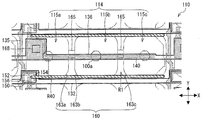
- FIG. 11 includes an active matrix substrate including a pixel electrode 160 having a plurality of subpixel electrodes 163a, 163b, and 163c and a cutout region R1, and a counter substrate including a rib (rivet) or a notch.
- a rib resistivet
- FIG. 11 shows a schematic configuration of a conventional liquid crystal display device 110.
- the horizontally long picture element 114 is divided into three subpixels 115a, 115b, and 115c almost equally in the long side direction, and the picture element electrode 160 is also divided into the subpixels 115a.
- the subpixel electrodes 163a, 163b and 163c are divided into substantially equal sizes.
- the subpixel electrodes 163a, 163b, and 163c are formed in a substantially square shape. Between the subpixel electrode 163a and the subpixel electrode 163b, and between the subpixel electrode 163b and the subpixel electrode 163c, A cutout region R1, which is a region from which the pixel electrode 160 has been cut out, is formed.
- the TFT 150 including the gate electrode 152, the source electrode 154, and the drain electrode 156 is provided for each picture element 114, and the subpixel electrode 163 a is electrically connected to the drain electrode 156 of the TFT 150 through the contact hole 168. It is connected to the.
- subpixel electrode 163a and the subpixel electrode 163b separated by the cutout region R1 are electrically connected by the subpixel electrode connection portion 165, and similarly, separated by the cutout region R1.
- the subpixel electrode 163b and the subpixel electrode 163c are also electrically connected by the subpixel electrode connection portion 165.
- the three subpixel electrodes 163a, 163b, and 163c are all electrically connected to the drain electrode 156 of the TFT 150 via the contact hole 168.
- a scanning signal line 132 electrically connected to the gate electrode 152 is formed in the lower region of the horizontally long picture element 114 in the X direction (horizontal direction) in FIG.
- a storage capacitor line 136 formed of the same layer as the gate electrode 152 is formed in a direction parallel to the scanning signal line 132, and the left end region of the picture element 114 has a Y direction (vertical A data signal line 135 electrically connected to the source electrode 154 is formed in the direction).
- a storage capacitor counter electrode 140 electrically connected to the drain electrode 156 through an insulating layer is formed so as to overlap the storage capacitor line 136 in plan view.
- a rib 100a (rivet) or a notch is provided so as to be positioned at the approximate center of the subpixel electrodes 163a, 163b, and 163c. It has been.
- the active matrix substrate and the counter substrate are provided with alignment dividing means, a liquid crystal display device having a wide viewing angle characteristic can be realized.
- the scanning signal line 132 is provided between adjacent picture element electrodes 160.
- the scanning signal line 132 is provided in the liquid crystal display device 110 having the horizontally long picture element 114.
- the distance that 132 and the pixel electrode 160 are close to each other is long. Accordingly, in the liquid crystal display device 110, an oblique electric field is generated in the region R40 where the scanning signal line 132 and the pixel electrode 160 face each other. In this region, the alignment of liquid crystal molecules is disturbed, and thus light leakage occurs. There arises a problem that roughness and display unevenness are likely to occur due to this.
- the scanning signal line 132 is provided in a substantially central region of the picture element 114 so as to shield the electric field of the scanning signal line 132 that causes the alignment disorder of the liquid crystal molecules.
- the subpixel electrodes 163a, 163b, and 163c are formed in the same layer as the subpixel electrodes 163a, 163b, and 163c in order to shield the electric field of the scanning signal line 132. Since the electrode connection portion 165 is used, the position where the electrode connection portion 165 is provided is limited to the scanning signal line 132.
- the sub-pixel electrodes 163a, 163b, and 163c provided on the scanning signal line 132 and the counter substrate side are considered.
- the ribs 100a (rivets) or the notches that are the orientation dividing means are arranged so as to overlap in a plan view.
- the electrode connection portion 165 that electrically connects the subpixel electrode 163a and the subpixel electrode 163b, and the electrode connection portion 165 that electrically connects the subpixel electrode 163b and the subpixel electrode 163c are the counter substrate. It is formed on a rib 100a (rivet) that is an orientation dividing means of the subpixel electrodes 163a, 163b, and 163c provided on the side, or on a virtual straight line that connects the notches.
- the pixel electrode 160 including the subpixel electrodes 163a, 163b, and 163c and the electrode connection portion 165 is provided.
- the shape is limited, and the shape of the cutout region R1 is also limited. Therefore, there is a problem that the cutout region R1 of the pixel electrode 160 having an optimized shape cannot be formed in the alignment division of the liquid crystal molecules.
- the present invention has been made in view of the above problems, and an object of the present invention is to provide a liquid crystal display panel and a liquid crystal display device that have a wide viewing angle characteristic and can perform high-quality display.
- the liquid crystal display panel of the present invention is electrically connected to a plurality of scanning signal lines, a plurality of data signal lines intersecting with the scanning signal lines, the scanning signal lines, and the data signal lines.
- a first insulating substrate including a plurality of transistor elements connected to the first insulating substrate; a second insulating substrate formed to face the first insulating substrate; the first insulating substrate; and the second insulating substrate.
- a liquid crystal display panel provided between each of the plurality of picture elements arranged in a matrix on the first insulating substrate.
- each pixel electrode provided corresponding to each pixel is electrically connected to the drain electrode of the transistor element provided in each pixel, and the pixel electrode formation layer and The formation layer of the data signal line is the scanning
- the pixel electrode and the scanning signal line are formed so as to overlap each other in the plan view in the pixel electrode formation region of each pixel.
- a notch is formed in the pixel electrode, and the shield electrode is formed by the formation layer of the data signal line.
- a part of the scanning signal line is provided so that at least a part thereof overlaps in a plan view.
- the pixel electrode and the scanning signal line are formed so as to overlap in plan view. That is, in the pixel electrode formation region of each picture element, the scanning signal line is covered by the picture element electrode that is an upper layer than the scanning signal line, and therefore, according to the scanning signal of the scanning signal line. In this configuration, disorder of the alignment of liquid crystal molecules due to the influence of an electric field can be suppressed.
- the shield electrode formed of the data signal line forming layer has a configuration in which at least a part thereof is overlapped in a plan view.
- the alignment of liquid crystal molecules due to the influence of the electric field of the scanning signal line to which a signal different from that of the pixel electrode is supplied is prevented in the formation layer of the pixel electrode and the data signal line. It has the structure which suppresses with the said shield electrode currently formed.
- the alignment disorder region due to the scanning signal line can be shielded, so that the display quality is improved, for example, the contrast is improved and the afterimage is reduced. To do.
- the pixel electrode can be formed in an optimized shape in the alignment division of the liquid crystal molecules.
- a liquid crystal display panel having a wide viewing angle characteristic and capable of high-quality display can be realized.
- the liquid crystal display device of the present invention is characterized by including the liquid crystal display panel in order to solve the above-described problems.
- a liquid crystal display device having a wide viewing angle characteristic and capable of high-quality display can be realized.
- each pixel electrode provided corresponding to each pixel is electrically connected to the drain electrode of the transistor element provided in each pixel.
- the pixel electrode formation layer and the data signal line formation layer are formed above the scan signal line formation layer.
- the element electrode and the scanning signal line are formed so as to overlap in a plan view, and a notch is formed in the pixel electrode in a portion where the pixel electrode and the scanning signal line overlap,
- the shield electrode is formed of the formation layer of the data signal line, and is configured to overlap with at least a part of the scanning signal line of the notch in a plan view.
- liquid crystal display device of the present invention has the above-described liquid crystal display panel as described above.
- FIG. 2 is a cross-sectional view taken along line AA in FIG.
- FIG. 2 is a plan view when the shield electrode is not provided in the liquid crystal display panel shown in FIG. 1.
- FIG. 5 is a diagram for explaining a case where a broken line portion (defect portion) is generated in a part of a data signal line of the liquid crystal display panel shown in FIG. 4 and repaired using a shield electrode.
- FIG. 7 is a diagram for explaining a case where a broken line portion (defect portion) is generated in a part of a data signal line of the liquid crystal display panel shown in FIG. 6 and repaired using a shield electrode. It is a top view which shows the schematic shape of the picture element part in the liquid crystal display panel of further another embodiment of this invention. In the case where a broken line portion (defect portion) is generated in a part of the data signal line of the liquid crystal display panel shown in FIG. FIG. It is a top view which shows the schematic shape of the picture element part in the liquid crystal display panel of further another embodiment of this invention. It is a figure which shows schematic structure of the conventional liquid crystal display device. It is a figure which shows schematic structure of the conventional liquid crystal display device. It is a figure which shows schematic structure of the conventional liquid crystal display device which provided the spare wiring for a repair outside a display area.
- a VA (Vertical Alignment) liquid crystal display panel having a pixel electrode structure having a CPA (Continuous Pinwheel Alignment) structure will be described as an example.
- the present invention is not limited to this.
- a pixel formation region such as a picture element electrode having a slit of Multidomain Vertical Alignment), a comb-like picture element electrode of IPS (In Plane Switching) and TBA (Transverse Bend Alignment) type, a fishbone shape picture element electrode,
- the scanning signal line is not covered by the pixel electrode (or sub-pixel electrode), and scanning is not covered by the pixel electrode (or sub-pixel electrode) in each pixel. Route if there is, it is possible to apply the present invention.
- the CPA structure is such that, for example, the common electrode provided on the counter substrate is provided with a protrusion or a notch so that the alignment control object is positioned at the center of each pixel, and is opposed to the counter substrate.
- the pixel electrodes provided on the active matrix substrate to be arranged are also formed in a shape along the alignment restriction object, and thereby the liquid crystal is continuously aligned in all directions between the alignment restriction objects.
- the TBA method refers to a mode in which liquid crystal molecules are vertically aligned with a horizontal electric field. That is, like the IPS method, a comb-like pixel electrode and a counter electrode are provided on the active matrix substrate side, and liquid crystal molecules are controlled by a horizontal electric field. It is a system that is controlled in the vertical direction, such as the VA system.
- FIG. 2 is a diagram showing a schematic configuration of the liquid crystal display panel 1 according to the embodiment of the present invention.
- the liquid crystal display panel 1 includes an array substrate 9 as a first substrate (first insulating substrate) and a counter substrate 16 as a second substrate (second insulating substrate).
- a liquid crystal layer 17 made of a liquid crystal material having negative dielectric anisotropy is sandwiched.
- the array substrate 9 includes a glass substrate 2 as an insulating substrate, a TFT element (transistor element) (not shown) formed on the glass substrate 2, and a scan electrically connected to the gate electrode of the TFT element.
- the auxiliary capacitor opposing wiring 4 is electrically connected to a drain electrode of a TFT element (not shown).
- a contact hole 6 is formed in the interlayer insulating film 5 (second insulating layer) formed on the storage capacitor counter wiring 4, and a pixel electrode 7 is formed on the interlayer insulating film 5.
- the pixel electrode 7 is electrically connected to the auxiliary capacitor facing wiring 4 through the contact hole 6. Then, a vertical alignment film is formed on the pixel electrode 7.
- the counter substrate 16 has a glass substrate 10 as an insulating substrate, and a black matrix 11 and color filter layers 12R, 12G, and 12B are formed on the glass substrate 10, and the color filter layers 12R and 12G are formed.
- the common electrode 13 is provided so as to cover the entire surface of 12B.
- a protrusion 14 that is a protrusion-like structure is formed on the common electrode 13 as an orientation dividing means.
- the present invention is not limited to this, and an incision (notch) in which the common electrode 13 is incised. ) Can also be used as orientation dividing means.
- the cross-sectional shape of the protrusion part 14 is not limited to the shape shown in FIG. 2, The cross-sectional shape may be triangular shape or trapezoid shape, for example.
- the position where the orientation dividing means is provided on the counter substrate 16 is considered in consideration of the aperture ratio of the liquid crystal display panel.
- the orientation dividing means is provided so that a part thereof overlaps in plan view, it is not limited to this.
- the protrusion 14 is formed in a predetermined shape using a photosensitive resist having a high transmittance in the visible light region, but is not limited thereto.
- red, green, and blue color filter layers 12R, 12G, and 12B are connected to the glass substrate 10 with respect to the pixel electrode 7 provided for each pixel of the array substrate 9.
- the present invention is not limited to this, and a COA (Color Filter On Array) structure in which the color filter layers 12R, 12G, and 12B are provided on the array substrate 9 side may be employed.
- a vertical alignment film 15 is formed on the surface of the common electrode 13 and the protrusion 14 on the side in contact with the liquid crystal layer 17.
- polarizing plates are respectively provided on the surface of the array substrate 9 opposite to the side in contact with the liquid crystal layer 17 and the surface of the counter substrate 16 opposite to the side in contact with the liquid crystal layer 17. It has been.
- the liquid crystal display panel 1 as described above, a backlight that irradiates the liquid crystal display panel 1 with uniform light, and the liquid crystal display panel 1 are driven.
- the drive circuit and power supply circuit are provided.
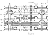
- FIG. 1 is a plan view showing a schematic shape of a picture element portion in a liquid crystal display panel 1 according to an embodiment of the present invention.
- FIG. 3 is a plan view showing a schematic shape of the picture element portion in the liquid crystal display panel 1a not provided with the shield electrodes 4a and 4b.
- each formation layer shows the vertical relationship when the pixel electrode 7 is removed.
- the liquid crystal display panel 1 has each pixel P (n, n + 1), P (n, n),... Arranged in a matrix.
- An element 18 (gate electrode 18G, source electrode 18S, drain electrode 18D) is provided.
- the liquid crystal display panel 1 is provided with a plurality of data signal lines SLn, SLn + 1,... And a plurality of scanning signal lines GLn, GLn + 1,.
- TFT elements 18 are provided at intersections between SLn + 1... And scanning signal lines GLn, GLn + 1.
- An image signal input from a data signal line driving circuit is sequentially supplied with a high level scanning signal from a scanning signal line driving circuit (not shown) to each scanning signal line GLn, GLn + 1, etc.
- a scanning signal line driving circuit not shown
- the TFT elements 18 connected to the signal lines GLn, GLn + 1,... are turned ON, the TFT elements 18 are connected via the source electrodes 18S of the TFT elements 18 connected to the data signal lines SLn, SLn + 1,.
- the pixel electrode 7 is connected to the drain electrode 18D.
- the drain electrode 18D of the TFT element 18 is electrically connected to the auxiliary capacitor counter wiring 4.
- the auxiliary capacitor opposing wiring 4 and the picture element electrode 7 are electrically connected through a contact hole 6 provided at a substantially central portion of each picture element P (n, n + 1), P (n, n). It has been configured.
- the auxiliary capacitance to be formed is provided for each pixel P (n, n + 1), P (n, n)..., But is not limited to this, and the auxiliary capacitance is necessary. It may be provided accordingly and can be omitted as appropriate.
- the length of the pixel electrode 7 in the direction parallel to the scanning signal lines GLn, GLn + 1,... Is the data signal line SLn, SLn + 1 of the pixel electrode 7.
- This is a so-called horizontally elongated picture element electrode 7 that is formed longer than the length in the direction parallel to.
- the pixel electrode 7 is provided with two notches 7a and 7b, and one of the two notches 7a and 7b is notched from above in the figure.
- the other 7b of the two notches 7a and 7b is cut out from the lower direction in the figure.
- the two notches 7a and 7b pattern the pixel electrode 7 so that a part of the pixel electrode 7 remains so that the pixel electrode 7 is not completely separated.
- the orientation of liquid crystal molecules due to the influence of the electric field of the scanning signal lines GLn, GLn + 1,... Not covered with the picture element electrode 7 in the two notches 7a and 7b of the picture element electrode 7 is changed.
- the auxiliary capacitor facing wiring 4 is extended to the positions of the scanning signal lines GLn, GLn + 1,... That are not covered with the pixel electrode 7 in the two notches 7a and 7b of the pixel electrode 7.
- the shield electrodes 4 a and 4 b are formed in the same layer as the auxiliary capacitor opposing wiring 4.
- the disturbance of the alignment of the liquid crystal molecules due to the influence of the electric field of the scanning signal lines GLn, GLn + 1, is configured to be suppressed by shield electrodes 4a and 4b formed by the formation layer of SLn + 1.
- the pixel electrode 7 is optimal in the alignment division of the liquid crystal molecules. It can be formed into a shaped shape.
- the shield electrodes 4a and 4b are supplied to the pixel electrode 7 because they are electrically connected to the drain electrode 18D of the TFT element 18 to which the pixel electrode 7 is electrically connected. Since the signal can be supplied also to the shield electrodes 4a and 4b, the liquid crystal display panel 1 capable of displaying with higher quality can be realized.
- the shield electrodes 4a and 4b are provided by extending the auxiliary capacitor opposing wiring 4.
- scanning that is not covered by the pixel electrode 7 in the two notches 7a and 7b of the pixel electrode 7 is performed.
- a shield electrode formed in the same layer as the drain electrode 18D of the TFT element 18 and electrically connected to the drain electrode 18D may be provided at the signal lines GLn, GLn + 1,.
- a shield electrode that is formed in the same layer as the drain electrode 18D of the TFT element 18 and is not electrically connected to the drain electrode 18D may be provided.
- the scanning signal line GLn of the notch 7b In the present embodiment, at least one of the two notches 7a and 7b of the pixel electrode 7, and in the notch 7b shown in FIGS. 1 and 3, the scanning signal line GLn of the notch 7b.
- the pixel electrode 7 is notched so that a part of GLn + 1... Overlaps with the pixel electrode 7 in plan view.
- a part of the scanning signal lines GLn, GLn + 1,... Of the cutout portion 7b is formed so as to overlap the pixel electrode 7 in plan view.
- the formation area of the shield electrode 4b formed of the formation layer of SLn + 1... (Auxiliary capacitor opposing wiring 4) can be made smaller than the formation area of the shield electrode 4a.
- the parasitic capacitance formed by the shield electrode 4b and the scanning signal lines GLn, GLn + 1,... can be reduced.
- the auxiliary capacitance opposing wiring 4 is connected to the auxiliary capacitance wiring CSn ⁇ CSn + 1 at least in the notches 7a and 7b of the pixel electrode 7.
- the auxiliary capacitance opposing wiring 4 is connected to the auxiliary capacitance wiring CSn ⁇ CSn + 1 at least in the notches 7a and 7b of the pixel electrode 7.
- the auxiliary capacitance lines CSn and CSn + 1 are formed in the notched portions 7a and 7b of the picture element electrode 7, that is, the non-opening portions in the picture elements P (n, n + 1), P (n, n). .., And the gate electrode 7 in each pixel P (n, n + 1), P (n, n)... In the formation region (opening in each picture element), the formation area of the auxiliary capacitance lines CSn, CSn + 1.
- the liquid crystal display panel 1 having a high aperture ratio can be realized.
- the drain electrode 18D of the TFT element 18 protrudes and overlaps with the gate electrode 18G of the TFT element 18 in a plan view.
- a part of the auxiliary capacitor opposing line 4 protrudes to the right and overlaps with a part of the auxiliary capacity lines CSn, CSn + 1. That is, with respect to a part of the auxiliary capacitance lines CSn, CSn + 1,. That's fine.
- the potential of the pixel electrode 7 decreases when the TFT element 18 is turned off (scanning signal is deactivated) due to the parasitic capacitance Csd therebetween.
- This amount of potential decrease is referred to as a pull-in voltage ( ⁇ V), and S ⁇ V is an effective potential applied to the pixel, where S is the signal potential supplied to the pixel electrode 7.
- S is the signal potential supplied to the pixel electrode 7.
- the pull-in voltage ⁇ V Cgd ⁇ (VH ⁇ VL) / (Ccs + Csd + Cgd + Clc).
- the pull-in voltage ( ⁇ V) generated by the variation of the parasitic capacitance Cgd is relaxed by the variation of the auxiliary capacitance Ccs.
- the drain electrode 18D is formed so as to be shifted to the right with respect to the gate electrode 18G, the overlapping area in the plan view of the gate electrode 18G and the drain electrode 18D is reduced, so that the parasitic capacitance Cgd is reduced.
- the pull-in voltage ⁇ V is also reduced from the above-described formula, a part of the auxiliary capacitance lines CSn, CSn + 1... Formed in the same layer as the gate electrode 18G and the auxiliary capacitance opposite to the auxiliary capacitance formed in the same layer as the drain electrode 18D.
- the drain electrode 18D when the drain electrode 18D is formed to be shifted to the left with respect to the gate electrode 18G, the overlapping area in the plan view of the gate electrode 18G and the drain electrode 18D increases, and the parasitic capacitance Cgd increases. From the above formula, the pull-in voltage ⁇ V also increases, but a part of the auxiliary capacitance lines CSn, CSn + 1... Formed in the same layer as the gate electrode 18G and the auxiliary capacitance formed in the same layer as the drain electrode 18D. Since the overlapping area in plan view with a part of the wiring 4 also increases, the auxiliary capacitance Ccs increases, and the pull-in voltage ⁇ V decreases from the above-described equation. As a result, the change in the pull-in voltage ⁇ V can be suppressed. It is like that.
- FIG. 1 shows a case where the wiring pattern is formed as designed.
- the shield electrodes 4a and 4b are extended from the auxiliary capacitor facing wiring 4 electrically connected to the drain electrode 18D of the TFT element 18. Therefore, since the signal supplied to the pixel electrode 7 can also be supplied to the shield electrodes 4a and 4b, the liquid crystal display panel 1 capable of displaying with higher quality can be realized.
- the liquid crystal display panel 1 having a high aperture ratio is realized. be able to.
- the picture element electrode 7 in each picture element P (n, n + 1) ⁇ P (n, n)... Has two notches 7a and 7b.
- the number, position, shape, and the like of the notch portions are not limited to this, and can be changed as appropriate.
- the scanning signal line GLn + 1 is electrically connected to the drain electrode 18D of the TFT element 18 electrically connected to the scanning signal line GLn.
- the present invention is not limited to this.
- the scanning signal line GLn is electrically connected to the scanning signal line GLn.
- the pixel electrode 7 electrically connected to the drain electrode 18D of the element 18 may overlap with the pixel electrode 7 in plan view.
- the shield electrodes 4a and 4b having regions not covered by the pixel electrodes 7 are formed in a layer different from the formation layer of the data signal lines SLn, SLn + 1,. It can also be used as an alignment pattern.
- the element can be formed using an element selected from W, Ti, Al, Cu, Cr, Nd, or the like, or an alloy material or a compound material containing the element as a main component, but is not limited thereto.
- the pixel electrode 7 can be formed of a conductive material such as ITO (Indium Tin Oxide) or IZO (Indium Zinc Oxide), but is not limited thereto.
- an inorganic insulating film is used as the gate insulating film 3 and a photosensitive organic insulating film is used as the interlayer insulating film 5.
- the present invention is not limited to this. Absent.
- the interlayer insulating film 5 is desirably thick and has a low dielectric constant. Specifically, the interlayer insulating film 5 preferably has a film thickness of, for example, 1 to 3 ⁇ m and a dielectric constant of 2 to 5. However, it is not limited to this.
- the pixel electrode 7 is formed on the formation layer of the data signal lines SLn, SLn + 1,... Via the interlayer insulating film 5, the scanning signal line GLn. Since the interlayer insulating film 5 is further provided as a shield layer that can suppress the disorder of the alignment of liquid crystal molecules due to the influence of the electric field of GLn + 1..., It has a wide viewing angle characteristic and a high-quality display The liquid crystal display panel 1 that can be realized can be realized.
- the shield electrode 4c is formed to extend from one of the auxiliary capacitor opposing wirings 4 of the nearest neighboring pixel in the direction in which the data signal lines SLn, SLn + 1,.
- the second embodiment is different from the first embodiment, and other configurations are the same as described in the first embodiment.
- members having the same functions as those shown in the drawings of the first embodiment are given the same reference numerals, and descriptions thereof are omitted.
- FIG. 4 is a plan view showing a schematic shape of a picture element portion in the liquid crystal display panel 1b according to the embodiment of the present invention.
- each formation layer shows the vertical relationship when the pixel electrode 7 is removed.
- the shield electrode 4c provided in the liquid crystal display panel 1b is provided with any of the adjacent picture elements in the direction (vertical direction in the figure) in which the data signal lines SLn, SLn + 1,.
- P (n, n + 1) FIG. 4 shows the case where the most adjacent picture element is the upper picture element is extended and formed from the auxiliary capacitance opposing wiring 4.
- the shield electrode 4c provided on the picture element P (n, n) is the nearest neighbor picture element in the direction in which the data signal lines SLn, SLn + 1,.
- the auxiliary capacitor opposing wiring 4 provided in one of the picture elements P (n, n + 1) is formed and extended.
- the liquid crystal display panel provided with two scanning signal line driving circuits so that the same scanning signal can be supplied to each scanning signal line GLn, GLn + 1.
- a broken line portion (defect portion) occurs in a part of SLn ⁇ SLn + 1..., It extends from the auxiliary capacitance counter wiring 4 provided in the picture element P (n, n + 1) which is one of the nearest neighbor picture elements.
- the shield electrode 4c provided and formed can be used in place of a part of the data signal lines SLn, SLn + 1,.
- FIG. 5 is a diagram for explaining a case where a broken line portion (defect portion) is generated in a part of the data signal line SLn + 1 of the liquid crystal display panel 1b and repaired using the shield electrode 4c.
- ⁇ indicates a location that is electrically connected using a laser
- X indicates a location that is appropriately electrically disconnected using a laser
- the shield electrode 4c provided in the picture element P (n, n), the scanning signal line GLn + 1, the auxiliary capacitance lines CSn / CSn + 1, the data signal line SLn + 1, and the auxiliary capacitance counter wiring 4 Can be used to repair a broken line portion (defect portion) generated in a part of the data signal line SLn + 1.
- a dotted line in FIG. 5 indicates a path through which the data signal is transmitted while avoiding a broken line portion (defect portion) generated in a part of the data signal line SLn + 1.
- the data signal includes the auxiliary capacitance line CSn and the picture element P. Transmission is performed via the storage capacitor counter wiring 4 at (n, n), the scanning signal line GLn + 1, the shield electrode 4c, the storage capacitor counter wiring 4 at the pixel P (n, n + 1), and the storage capacitor wiring CSn + 1. It has come to be.
- the repaired data signal line SLn + 1 can secure the same charging rate as that of the normal data signal line SLn.
- a luminance difference is not visually recognized between the picture element electrically connected to the line SLn + 1 and the picture element electrically connected to the normal data signal line SLn...
- a liquid crystal display panel 1b capable of high-quality display can be realized.
- the scanning signal lines GLn, GLn + 1,... are repaired by being electrically connected and disconnected using a laser, the scanning signal lines GLn, GLn + 1,.
- the same scanning signal can be sequentially supplied to both ends of the scanning signal lines GLn, GLn + 1,... From both ends of the scanning signal lines GLn, GLn + 1,.
- the two scanning signal line driving circuits are monolithically formed on the liquid crystal display panel 1b using the gate driver monolithic (GDM) technique, but the present invention is not limited to this, and the scanning signal line is not limited thereto.
- the drive circuit may be externally provided on the liquid crystal display panel 1b.
- a large-sized liquid crystal display panel, a high-definition liquid crystal display panel, or a liquid crystal display panel having a triple scan structure (a structure in which one pixel is formed by arranging horizontally long picture elements in the direction in which the data signal lines extend)
- the panel load resistance, capacity
- a spare wiring for repair is provided outside the display area, it cannot be repaired due to signal delay, etc. In some cases, the yield was reduced.
- the data signal line can be repaired without causing the problem of signal delay and without being affected by the load (resistance, capacitance) of the panel. It can be formed thin, and the transmittance of the liquid crystal display panel can be improved. Further, unlike the prior art, it is not necessary to provide spare wiring for repair outside the display area, so that a narrow frame of the liquid crystal display panel can be realized.
- the scanning signal lines GLn, GLn + 1... are not overlapped with the notches 7a and 7b in the plan view in at least one of the notches 7a and 7b of the picture element electrode 7.
- the scanning signal lines GLn, GLn + 1,... Formed at the boundary between any one of the adjacent pixels in the direction in which the data signal lines SLn, SLn + 1. ..
- FIG. 6 is a plan view showing a schematic shape of a picture element portion in the liquid crystal display panel 1c according to the embodiment of the present invention.
- each formation layer has shown the vertical relationship when the pixel electrode 7 is remove
- the scanning signal lines GLn, GLn + 1... are bent at the cutout portions 7a of the pixel electrodes 7 so as not to overlap with the cutout portions 7a.
- P (n, n + 1) which is one of the nearest neighboring picture elements in the direction in which the data signal lines SLn, SLn + 1,.
- Shield electrode formed by extending from a part of the scanning signal line GLn + 1 formed at the boundary with (n, n) and the auxiliary capacitance opposing wiring 4 of the one nearest neighbor pixel P (n, n + 1) 4d is formed so that at least a part thereof overlaps in plan view.
- the overlapping area of the shield electrode 4d and the picture element electrode 7 in plan view can be reduced.
- one of the nearest neighboring picture elements can be connected to the picture element electrode 7 of the picture element P (n, n). It is possible to suppress the influence of the potential of the shield electrode 4d extending from the auxiliary capacitance opposing wiring 4 of the picture element P (n, n + 1). That is, the influence exerted on the pixel electrode 7 of the pixel P (n, n) held at a constant potential via the shield electrode 4d can be suppressed.
- FIG. 7 is a diagram for explaining a case where a broken line portion (defect portion) is generated in a part of the data signal line SLn + 1 of the liquid crystal display panel 1c and repaired using the shield electrode 4d.
- ⁇ indicates a location that is electrically connected using a laser
- X indicates a location that is appropriately electrically disconnected using a laser
- the shield electrode 4d provided at the boundary between the picture element P (n, n + 1) and the picture element P (n, n) and the notch 7a are bent so as not to overlap each other in plan view.
- the scanning signal line GLn + 1, the auxiliary capacitance lines CSn and CSn + 1, the data signal line SLn + 1, and the auxiliary capacitance counter wiring 4 formed in this manner a broken line portion (defect portion) generated in a part of the data signal line SLn + 1 ) Can be repaired.
- a dotted line in FIG. 7 indicates a path through which the data signal is transmitted while avoiding a broken line portion (defect portion) generated in a part of the data signal line SLn + 1.
- the data signal includes the auxiliary capacitance line CSn and the picture element P. (N, n) storage capacitor counter wiring 4, shield electrode 4b, scanning signal line GLn + 1, shield electrode 4d, storage capacitor counter wiring 4 in picture element P (n, n + 1), storage capacitor wiring CSn + 1, Are communicated through.
- the repaired data signal line SLn + 1 can be secured at a charge rate equivalent to that of the normal data signal line SLn... That has not been repaired.
- the repaired data signal line SLn + 1 can be secured.
- a luminance difference is not visually recognized between the picture element electrically connected to the line SLn + 1 and the picture element electrically connected to the normal data signal line SLn...
- a liquid crystal display panel 1c capable of high quality display can be realized.
- the scanning signal lines GLn, GLn + 1,... are repaired by electrically connecting and disconnecting them using a laser, the scanning signal lines GLn, GLn + 1,.
- the same scanning signal can be sequentially supplied to both ends of the scanning signal lines GLn, GLn + 1,... From both ends of the scanning signal lines GLn, GLn + 1,.
- the wiring including the shield electrode 4a extends to the boundary with either one of the adjacent picture elements in the direction in which the data signal lines SLn, SLn + 1, etc. extend to form the electrode 4e.
- the electrode 4e is extended from the auxiliary capacitive wiring CSn, CSn + 1,... Of the one of the most adjacent picture elements, and the counter electrode 19 of the formed electrode 4e is formed so as to at least partially overlap in plan view.
- the second embodiment is different from the first to third embodiments, and the other configurations are as described in the first to third embodiments.
- members having the same functions as those shown in the drawings of Embodiments 1 to 3 are given the same reference numerals, and descriptions thereof are omitted.
- FIG. 8 is a plan view showing a schematic shape of a picture element portion in the liquid crystal display panel 1d according to the embodiment of the present invention.
- each formation layer has shown the vertical relationship when the pixel electrode 7 is remove
- the data signal lines SLn, SLn + 1,... And the auxiliary capacitor facing wiring 4 formed in the same layer as the wiring including the shield electrode 4a are extended from the data signal lines SLn, SLn + 1,.
- the electrode 4e is formed to extend to the boundary between the nearest adjacent picture elements P (n, n + 1) ⁇ P (n, n) in the direction in which they are located (vertical direction in the figure).
- the electrode 4e and the scanning signal line GLn ... Extended from the auxiliary capacitance line CSn + 1 of the picture element P (n, n + 1) formed in the same layer as GLn + 1... So that the counter electrode 19 of the formed electrode 4e at least partially overlaps in plan view. Is formed.
- FIG. 9 shows a case where a broken line portion (defect portion) occurs in a part of the data signal line SLn + 1 of the liquid crystal display panel 1d, and is provided at the boundary between the nearest adjacent picture elements P (n, n + 1) ⁇ P (n, n) It is a figure for demonstrating the case where it repairs using the electrode 4e and the counter electrode 19.
- a circled portion indicates a portion that is electrically connected using a laser
- a portion X indicates a portion that is appropriately electrically disconnected using a laser.
- the electrode 4e provided at the boundary between the picture element P (n, n + 1) and the picture element P (n, n), the counter electrode 19 of the electrode 4e, the auxiliary capacitance lines CSn and CSn + 1,
- the data signal line SLn + 1 and the storage capacitor counter wiring 4 it is possible to repair a broken line portion (defect portion) generated in a part of the data signal line SLn + 1.
- a dotted line in FIG. 9 indicates a path through which the data signal is transmitted while avoiding a broken line portion (defect portion) generated in a part of the data signal line SLn + 1.
- the data signal includes the auxiliary capacitance line CSn and the pixel P Transmission is performed via the auxiliary capacitance counter wiring 4, the shield electrode 4e, the counter electrode 19, and the auxiliary capacitance wiring CSn + 1 in (n, n).
- the liquid crystal display panel 1d even if the data signal line SLn + 1 is restored, the charge rate equivalent to that of the normal data signal line SLn... That has not been restored can be secured. A luminance difference is not visually recognized between the picture element electrically connected to the line SLn + 1 and the picture element electrically connected to the normal data signal line SLn... A liquid crystal display panel 1d capable of high-quality display can be realized.
- the broken line portions (defect portions) of the data signal lines SLn, SLn + 1,... Can be repaired without using the scanning signal lines GLn, GLn + 1,. It is not necessary to provide two scanning signal line drive circuits so that the same scanning signal can be supplied from both ends to the scanning signal lines GLn, GLn + 1.
- liquid crystal display panel 1d capable of realizing the narrowing of the frame area and displaying high quality.
- each of the pixel elements P (n, n + 1), P (n, n)... Is provided with a plurality of sub-pixel electrodes 20a, 20b, and 20c that are electrically separated by a notch 20d.
- the sub picture element electrodes 20a, 20b, 20c are electrically connected to the drain electrode 18D of the transistor element 18 provided in the picture elements P (n, n + 1), P (n, n).
- this embodiment is different from the first to fourth embodiments, and the other configurations are as described in the first to fourth embodiments.
- members having the same functions as those shown in the drawings of Embodiments 1 to 4 are given the same reference numerals, and descriptions thereof are omitted.
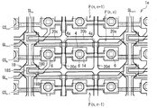
- FIG. 10 is a plan view showing a schematic shape of the picture element portion including the sub picture element electrodes 20a, 20b, and 20c in the liquid crystal display panel 1e according to the embodiment of the present invention.
- each formation layer has shown the vertical relationship at the time of excluding sub pixel electrode 20a * 20b * 20c.
- the sub picture element electrodes 20a, 20b and 20c are formed.
- each of the plurality of sub picture element electrodes 20a, 20b, and 20c is electrically connected to the drain electrode 18D of the transistor element 18 through the contact hole 6 formed in the interlayer insulating film 5. Since the capacitor facing wiring 4 is electrically connected, it is not necessary to provide a separate connecting portion between the plurality of sub picture element electrodes 20a, 20b, and 20c as in the first to fourth embodiments. .
- connection portion is known to have an adverse effect on the afterimage and response speed in the liquid crystal display panel. According to the above configuration, the connection portion is separately provided between the plurality of sub-pixel electrodes 20a, 20b, and 20c. Therefore, the liquid crystal display panel 1e with improved afterimage and response speed can be realized.
- the notch portion 20d is not provided with a connection portion, the scanning signal lines GLn, GLn + 1,... That are not covered by the plurality of sub-pixel electrodes 20a, 20b, 20c. Is covered with a shield electrode 4a formed of a formation layer of the data signal lines SLn, SLn + 1... (Auxiliary capacitor opposing wiring 4).
- three electrically isolated sub-pixel electrodes 20a, 20b, and 20c are formed in each pixel P (n, n + 1), P (n, n).
- the present invention is not limited to this.
- a connection portion is provided only between the sub-pixel electrode 20a and the sub-pixel electrode 20b, and the sub-pixel electrode 20a and the sub-pixel electrode 20b are Alternatively, it may be configured such that only the sub-pixel electrode 20c is electrically separated from the sub-pixel electrode 20a and the sub-pixel electrode 20b.
- the shield electrode 4a is formed by extending from the auxiliary capacitance opposing wiring 4 of the picture element P (n, n), but the shield electrode 4a , In the direction in which the data signal lines SLn, SLn + 1,... Are extended (vertical direction in the drawing), the nearest neighboring picture element P (n, n + 1) .P (n , N-1), and can be formed by extending from one of the auxiliary capacitor counter wirings 4.
- the shield electrode 4a is formed by extending from one of the auxiliary capacitance opposing wirings 4 which are the most adjacent picture elements P (n, n + 1) and P (n, n-1), as described above.
- P (n, n + 1) and P (n, n-1) are the most adjacent picture elements P (n, n + 1) and P (n, n-1), as described above.
- a broken line portion (defect portion) occurs in a part of the data signal lines SLn, SLn + 1,..., The broken line portion can be repaired using the shield electrode 4a.
- each of the pixel electrodes is a plurality of sub-pixel electrodes electrically separated by the notch, and each of the plurality of sub-pixel electrodes is any of the pixel elements. It is preferable to be electrically connected to the drain electrode of the transistor element provided in the.
- each of the pixel electrodes is formed of a plurality of sub-pixel electrodes that are electrically separated by the notch.
- each of the plurality of sub picture element electrodes is electrically connected to the drain electrode of the transistor element provided in each picture element, a separate connection portion is provided between the plurality of sub picture element electrodes. There is no need.
- connection portion provided separately between the plurality of sub picture element electrodes has an adverse effect on the afterimage and response speed in the liquid crystal display panel. Since a separate connection portion is not required between the pixel electrodes, a liquid crystal display panel with improved afterimage and response speed can be realized.
- the shield electrode is electrically connected to the drain electrode of the transistor element.
- the shield electrode is electrically connected to the drain electrode of the transistor element to which the pixel electrode or the plurality of sub-pixel electrodes are electrically connected. Since the signal supplied to the element electrode or the plurality of sub picture element electrodes can be supplied to the shield electrode, a liquid crystal display panel capable of displaying with higher quality can be realized.
- the length of each pixel electrode in the direction parallel to the scanning signal line is longer than the length of the pixel electrode in the direction parallel to the data signal line. preferable.
- the ratio of the scanning signal lines in each picture element increases, so that the alignment of liquid crystal molecules due to the influence of the electric field of the scanning signal lines is disturbed.
- the structure of suppressing by the shield electrode formed of the pixel electrode and the data signal line forming layer is more effective.
- the vertically long picture elements are arranged in the direction in which the scanning signal lines are extended.
- the number of the data signal lines can be reduced.
- a data signal line driving circuit consumes more power and has a higher manufacturing cost than a scanning signal line driving circuit. Therefore, by reducing the number of data signal lines, the power consumption and manufacturing cost of the data signal line driving circuit can be reduced. Can be reduced.
- At least one of the cutout portions of the pixel electrode has the picture signal so that a part of the scanning signal line of the cutout portion overlaps the pixel electrode in plan view.
- the element electrode is preferably cut out.
- the notched portion of the pixel electrode is configured to be cut out so that a part of the scanning signal line of the notched portion overlaps the pixel electrode in plan view.
- a part of the scanning signal line of the cutout portion is formed so as to overlap with the pixel electrode in plan view.
- the formation area of the shield electrode formed of the formation layer can be reduced.
- the parasitic capacitance formed by the shield electrode and the scanning signal line can be reduced.
- the auxiliary capacitance wiring and the auxiliary capacitance counter wiring are formed so as to overlap the pixel electrode in plan view.
- the auxiliary capacitance wiring is formed in the same layer as the scanning signal line forming layer and in parallel with the scanning signal line, and the auxiliary capacitance facing wiring is formed at least in the notched portion of the pixel electrode.
- the wiring layer is formed in the same layer as the data signal line forming layer via the first insulating layer so as to overlap the wiring in a plan view.
- the auxiliary capacitance wiring formed in the same layer as the scanning signal line formation layer at least in the notch portion of the pixel electrode forms the data signal line via the first insulating layer. It is formed so as to overlap with the storage capacitor counter wiring formed in the same layer as the layer in plan view.
- a notch portion of the pixel electrode that is, a non-opening portion in the pixel element can secure an auxiliary capacitance composed of the auxiliary capacitance wiring, the first insulating layer, and the auxiliary capacitance counter wiring. It is possible to reduce the formation area of the storage capacitor wiring and the storage capacitor counter wiring in the pixel electrode formation region (the opening in the pixel).
- the drain electrode when the drain electrode is formed with a deviation from a design value with respect to the scanning signal line including the gate electrode, the scanning signal line and the drain electrode overlap in plan view.
- the design value is the same as that of the scanning signal line so that the drain electrode has an overlap area in the plan view of the storage capacitor wiring and the storage capacitor counter wiring.
- they are shifted and overlapped in a certain direction, and a part of the auxiliary capacitor counter wiring is also shifted and overlapped in a certain direction in a plan view with respect to a part of the auxiliary capacitance line. It is preferable.
- the transistor element is turned off due to the parasitic capacitance Cgd between the drain electrode of the transistor element (and the pixel electrode electrically connected thereto) and the scanning signal line.
- a phenomenon is known in which the potential of a picture element (picture element electrode) decreases when the scanning signal is deactivated. This potential drop amount (absolute value) is called a pull-in voltage ( ⁇ V), and if the signal potential supplied to the picture element is S, S ⁇ V is an effective potential applied to the picture element.
- the active potential of the scanning signal supplied to the scanning signal line is VH
- the inactive potential is VL
- the liquid crystal capacitor is Clc
- the auxiliary capacitor is Ccs
- the design value of the wiring pattern is such that the drain electrode protrudes and overlaps with the gate electrode in the plan view, for example, in the right direction. If a part of the auxiliary capacitor counter wiring also protrudes to the right in a plan view and overlaps with a part of the gate electrode from the design value, the drain electrode When the formation pattern is shifted and a wiring pattern is formed, it is as follows.
- the drain electrode When the drain electrode is formed so as to be shifted in the right direction with respect to the gate electrode, the overlap area in the plan view of the gate electrode and the drain electrode is reduced, so that the parasitic capacitance Cgd is reduced.
- the pull-in voltage ⁇ V is also reduced from the equation, but the plane of a part of the auxiliary capacity wiring formed in the same layer as the gate electrode and a part of the auxiliary capacity opposing wiring formed in the same layer as the drain electrode Since the overlapping area in view also decreases, the auxiliary capacitance Ccs decreases, and the pull-in voltage ⁇ V increases from the above-described equation. As a result, the change in the pull-in voltage ⁇ V can be suppressed.
- the pull-in voltage ⁇ V also increases from the above formula, but a part of the auxiliary capacitance wiring formed in the same layer as the gate electrode and a part of the auxiliary capacitance counter wiring formed in the same layer as the drain electrode. Since the overlapping area in plan view also increases, the auxiliary capacitance Ccs increases, and the pull-in voltage ⁇ V decreases from the above-described equation. As a result, the change in the pull-in voltage ⁇ V can be suppressed. .
- the shield electrode is formed to extend from the auxiliary capacitor facing wiring at the notch portion of the pixel electrode.
- the shield electrode extends from the auxiliary capacitor facing wiring electrically connected to the drain electrode of the transistor element, a signal supplied to the pixel electrode is transmitted. Since it can supply also to the above-mentioned shield electrode, a liquid crystal display panel which can display higher quality can be realized.
- the shield electrode is formed by extending from the auxiliary capacitor facing wiring in the notch portion of the pixel electrode, a liquid crystal display panel having a high aperture ratio can be realized.
- the shield electrode may be formed to extend from the auxiliary capacitor facing wiring of any one of the adjacent picture elements in the direction in which the data signal line extends. preferable.
- the shield electrode is formed by extending from the auxiliary capacitance facing wiring of any one of the adjacent pixels in the direction in which the data signal line is extended.
- a liquid crystal display panel having angular characteristics and capable of high-quality display can be realized.
- a broken line is formed at a part of the data signal line.
- the shield electrode can be used in place of a part of the data signal line having the broken line portion.
- the broken line portion of the data signal line can be repaired using the shield electrode in the picture element, the conventional configuration in which spare wiring for repair is provided outside the display area is used. In comparison, the influence of signal delay can be kept low. Therefore, even with the repaired data signal line, it is possible to ensure a charge rate equivalent to that of a normal data signal line that has not been repaired, so that the picture element electrically connected to the repaired data signal line
- a liquid crystal display panel can be realized in which a luminance difference is not visually recognized with respect to a picture element electrically connected to a normal data signal line that has not been repaired, and high-quality display is possible.
- the scanning signal line is formed by bending at least one of the cutout portions of the pixel electrode so as not to overlap the cutout portion in plan view.
- a part of the scanning signal line formed at the boundary between any one of the adjacent pixels in the direction in which the data signal line extends and the pixel, and the auxiliary capacitance counter wiring of the adjacent pixel It is preferable that the shield electrode that is extended and formed so as to overlap at least partially in a plan view.
- the scanning signal line is formed by bending at least one of the cutout portions of the pixel electrode so as not to overlap the cutout portion in plan view.
- a part of the scanning signal line formed at the boundary between any one of the adjacent pixels in the extending direction and the pixel is connected to the auxiliary capacitor facing wiring of the one adjacent pixel.
- the extended shield electrode is formed so as to at least partly overlap in plan view.
- the overlapping area of the shield electrode and the pixel electrode in plan view can be reduced, and the pixel electrode is extended from the auxiliary capacitance facing wiring of the one nearest neighboring pixel.
- the influence of the potential of the shield electrode can be suppressed. That is, it is possible to suppress the influence exerted on the pixel electrode held at a constant potential via the shield electrode.
- liquid crystal display panel capable of displaying higher quality can be realized.
- a broken line is formed at a part of the data signal line.
- the shield electrode can be used in place of a part of the data signal line having the broken line portion.
- the broken line portion of the data signal line can be repaired using the shield electrode in the picture element, the conventional configuration in which spare wiring for repair is provided outside the display area is used. In comparison, the influence of signal delay can be kept low. Therefore, even with the repaired data signal line, it is possible to ensure a charge rate equivalent to that of a normal data signal line that has not been repaired, so that the picture element electrically connected to the repaired data signal line
- a liquid crystal display panel can be realized in which a luminance difference is not visually recognized with respect to a picture element electrically connected to a normal data signal line that has not been repaired, and high-quality display is possible.
- the same scanning signal can be sequentially supplied from both ends of each scanning signal line to both ends of the plurality of extending scanning signal lines. It is preferable that two scanning signal line driving circuits are provided.
- the two scanning signal line driving circuits are formed monolithically or externally so that the same scanning signal can be supplied from both ends to one scanning signal line.
- the shield electrode can be used as a substitute for a part of the data signal line having the broken line part.
- the shield electrode extends to the boundary between any one of the adjacent picture elements in the direction in which the data signal line extends and the picture element.
- the shield electrode and the counter electrode of the shield electrode formed and extended from the auxiliary capacitance wiring of the one nearest neighboring picture element are at least in plan view. It is preferable that they are formed so as to partially overlap.
- the auxiliary capacitance of the shield electrode and the one nearest neighbor pixel in the region that does not overlap the scanning signal line in plan view, that is, at the boundary between the one nearest neighbor pixel and the picture element, the auxiliary capacitance of the shield electrode and the one nearest neighbor pixel.
- the opposing electrode of the shield electrode formed extending from the wiring is formed so as to at least partially overlap in plan view.
- the data signal having the broken line portion is connected to the shield electrode and the counter electrode of the shield electrode without using the scanning signal line.
- the structure can be used as a substitute for part of the line.
- the broken line portion (defect portion) of the data signal line can be repaired without using the scanning signal line, the same scanning signal can be supplied from both ends to one scanning signal line. In addition, there is no need to provide two scanning signal line driving circuits.
- the broken line portion (defect portion) of the data signal line is repaired without using the scanning signal line, it is possible to reduce the repair time and work errors.
- the scanning signal line formed so as to overlap the pixel electrode formed on the picture element in plan view is the nearest neighboring pixel element in the direction in which the data signal line extends. It is preferable that the transistor element is electrically connected to the pixel electrode formed on either one of the transistor elements.
- the scanning signal line provided in the picture element is the picture element electrode provided on one of the nearest picture elements in the direction in which the data signal line extends. Or it is the structure electrically connected with the said transistor element electrically connected with the said some sub pixel electrode.
- the pixel electrode formation layer is formed on the data signal line formation layer via a second insulating layer.
- the second insulating layer is further provided as the shield layer that can suppress the disorder of the orientation of the liquid crystal molecules due to the influence of the electric field of the scanning signal line, A liquid crystal display panel capable of displaying high quality can be realized.
- the thickness of the second insulating layer is preferably thick and the dielectric constant is preferably low. Specifically, the thickness of the second insulating layer is, for example, 1 to 3 ⁇ m, and the dielectric constant is 2 to 5. However, it is not limited to this.
- a common electrode having protrusions and / or cutouts is formed on the surface of the second insulating substrate on the side in contact with the liquid crystal layer as alignment dividing means. .
- a liquid crystal display panel having a wide viewing angle characteristic can be realized.
- the present invention can be applied to a liquid crystal display panel and a liquid crystal display device.
Landscapes
- Physics & Mathematics (AREA)
- Nonlinear Science (AREA)
- Engineering & Computer Science (AREA)
- Microelectronics & Electronic Packaging (AREA)
- Mathematical Physics (AREA)
- Chemical & Material Sciences (AREA)
- Crystallography & Structural Chemistry (AREA)
- General Physics & Mathematics (AREA)
- Optics & Photonics (AREA)
- Liquid Crystal (AREA)
- Devices For Indicating Variable Information By Combining Individual Elements (AREA)
Abstract
Priority Applications (3)
| Application Number | Priority Date | Filing Date | Title |
|---|---|---|---|
| CN201180019832.2A CN102859430B (zh) | 2010-04-20 | 2011-02-18 | 液晶显示面板和液晶显示装置 |
| JP2012511577A JP5791593B2 (ja) | 2010-04-20 | 2011-02-18 | 液晶表示パネルおよび液晶表示装置 |
| US13/641,949 US9036121B2 (en) | 2010-04-20 | 2011-02-18 | Liquid crystal display panel and liquid crystal display device |
Applications Claiming Priority (2)
| Application Number | Priority Date | Filing Date | Title |
|---|---|---|---|
| JP2010097193 | 2010-04-20 | ||
| JP2010-097193 | 2010-04-20 |
Publications (1)
| Publication Number | Publication Date |
|---|---|
| WO2011132452A1 true WO2011132452A1 (fr) | 2011-10-27 |
Family
ID=44833992
Family Applications (1)
| Application Number | Title | Priority Date | Filing Date |
|---|---|---|---|
| PCT/JP2011/053539 Ceased WO2011132452A1 (fr) | 2010-04-20 | 2011-02-18 | Panneau d'affichage à cristaux liquides et dispositif d'affichage à cristaux liquides |
Country Status (4)
| Country | Link |
|---|---|
| US (1) | US9036121B2 (fr) |
| JP (1) | JP5791593B2 (fr) |
| CN (1) | CN102859430B (fr) |
| WO (1) | WO2011132452A1 (fr) |
Cited By (1)
| Publication number | Priority date | Publication date | Assignee | Title |
|---|---|---|---|---|
| KR20170023361A (ko) * | 2015-08-21 | 2017-03-03 | 삼성디스플레이 주식회사 | 표시장치 및 그의 수리방법 |
Families Citing this family (9)
| Publication number | Priority date | Publication date | Assignee | Title |
|---|---|---|---|---|
| JP6093575B2 (ja) | 2013-01-15 | 2017-03-08 | 株式会社ジャパンディスプレイ | 液晶表示装置 |
| FR3005763B1 (fr) | 2013-05-17 | 2016-10-14 | Fogale Nanotech | Dispositif et procede d'interface de commande capacitive adapte a la mise en œuvre d'electrodes de mesures fortement resistives |
| FR3028061B1 (fr) * | 2014-10-29 | 2016-12-30 | Fogale Nanotech | Dispositif capteur capacitif comprenant des electrodes ajourees |
| FR3032287B1 (fr) | 2015-02-04 | 2018-03-09 | Quickstep Technologies Llc | Dispositif de detection capacitif multicouches, et appareil comprenant le dispositif |
| CN108646477A (zh) * | 2018-03-27 | 2018-10-12 | 上海中航光电子有限公司 | 阵列基板、显示面板和显示装置 |
| JP2019184864A (ja) * | 2018-04-12 | 2019-10-24 | シャープ株式会社 | 表示装置 |
| TWI753527B (zh) * | 2020-08-12 | 2022-01-21 | 友達光電股份有限公司 | 顯示裝置 |
| CN115705821A (zh) * | 2021-08-11 | 2023-02-17 | 京东方科技集团股份有限公司 | 显示基板及其制备方法、显示装置 |
| CN117492288A (zh) * | 2023-02-03 | 2024-02-02 | Tcl华星光电技术有限公司 | 阵列基板及显示面板 |
Citations (7)
| Publication number | Priority date | Publication date | Assignee | Title |
|---|---|---|---|---|
| JP2000002889A (ja) * | 1998-06-16 | 2000-01-07 | Mitsubishi Electric Corp | 液晶表示装置 |
| JP2003228073A (ja) * | 2001-11-30 | 2003-08-15 | Sharp Corp | 液晶表示装置 |
| JP2005003916A (ja) * | 2003-06-11 | 2005-01-06 | Sharp Corp | 液晶表示装置 |
| JP2007128094A (ja) * | 2005-11-03 | 2007-05-24 | Samsung Electronics Co Ltd | 表示基板、これを具備する液晶表示パネル及び表示装置 |
| WO2009013855A1 (fr) * | 2007-07-20 | 2009-01-29 | Sharp Kabushiki Kaisha | Dispositif d'affichage à cristaux liquides |
| WO2009130819A1 (fr) * | 2008-04-22 | 2009-10-29 | シャープ株式会社 | Dispositif d'affichage à cristaux liquides |
| WO2009157157A1 (fr) * | 2008-06-24 | 2009-12-30 | シャープ株式会社 | Dispositif d’affichage à cristaux liquides |
Family Cites Families (7)
| Publication number | Priority date | Publication date | Assignee | Title |
|---|---|---|---|---|
| US6965422B2 (en) | 1998-07-24 | 2005-11-15 | Sharp Kabushiki Kaisha | Liquid crystal display device |
| KR100628263B1 (ko) * | 2002-08-21 | 2006-09-27 | 엘지.필립스 엘시디 주식회사 | 액정표시소자 |
| JP4483477B2 (ja) | 2004-08-23 | 2010-06-16 | セイコーエプソン株式会社 | 液晶表示装置及び電子機器 |
| JP4023746B2 (ja) | 2005-02-23 | 2007-12-19 | 日本発条株式会社 | ハード・ディスク・ドライブ用のベース及び製造方法 |
| CN100498490C (zh) * | 2007-09-13 | 2009-06-10 | 友达光电股份有限公司 | 液晶显示面板与像素 |
| US8736779B2 (en) * | 2008-11-19 | 2014-05-27 | Sharp Kabushiki Kaisha | Active matrix substrate, liquid crystal display panel, liquid crystal display device, method for manufacturing active matrix substrate, method for manufacturing liquid crystal display panel, and method for driving liquid crystal display panel |
| WO2010092706A1 (fr) | 2009-02-13 | 2010-08-19 | シャープ株式会社 | Substrat de réseau, dispositif d'affichage à cristaux liquides et dispositif électronique |
-
2011
- 2011-02-18 WO PCT/JP2011/053539 patent/WO2011132452A1/fr not_active Ceased
- 2011-02-18 US US13/641,949 patent/US9036121B2/en active Active
- 2011-02-18 CN CN201180019832.2A patent/CN102859430B/zh active Active
- 2011-02-18 JP JP2012511577A patent/JP5791593B2/ja active Active
Patent Citations (7)
| Publication number | Priority date | Publication date | Assignee | Title |
|---|---|---|---|---|
| JP2000002889A (ja) * | 1998-06-16 | 2000-01-07 | Mitsubishi Electric Corp | 液晶表示装置 |
| JP2003228073A (ja) * | 2001-11-30 | 2003-08-15 | Sharp Corp | 液晶表示装置 |
| JP2005003916A (ja) * | 2003-06-11 | 2005-01-06 | Sharp Corp | 液晶表示装置 |
| JP2007128094A (ja) * | 2005-11-03 | 2007-05-24 | Samsung Electronics Co Ltd | 表示基板、これを具備する液晶表示パネル及び表示装置 |
| WO2009013855A1 (fr) * | 2007-07-20 | 2009-01-29 | Sharp Kabushiki Kaisha | Dispositif d'affichage à cristaux liquides |
| WO2009130819A1 (fr) * | 2008-04-22 | 2009-10-29 | シャープ株式会社 | Dispositif d'affichage à cristaux liquides |
| WO2009157157A1 (fr) * | 2008-06-24 | 2009-12-30 | シャープ株式会社 | Dispositif d’affichage à cristaux liquides |
Cited By (2)
| Publication number | Priority date | Publication date | Assignee | Title |
|---|---|---|---|---|
| KR20170023361A (ko) * | 2015-08-21 | 2017-03-03 | 삼성디스플레이 주식회사 | 표시장치 및 그의 수리방법 |
| KR102418615B1 (ko) * | 2015-08-21 | 2022-07-11 | 삼성디스플레이 주식회사 | 표시장치 및 그의 수리방법 |
Also Published As
| Publication number | Publication date |
|---|---|
| CN102859430A (zh) | 2013-01-02 |
| US20130033469A1 (en) | 2013-02-07 |
| JP5791593B2 (ja) | 2015-10-07 |
| US9036121B2 (en) | 2015-05-19 |
| CN102859430B (zh) | 2015-07-08 |
| JPWO2011132452A1 (ja) | 2013-07-18 |
Similar Documents
| Publication | Publication Date | Title |
|---|---|---|
| JP5791593B2 (ja) | 液晶表示パネルおよび液晶表示装置 | |
| US9274384B2 (en) | Liquid-crystal display device | |
| JP5116879B2 (ja) | 液晶表示装置 | |
| US7388639B2 (en) | In-plane switching mode liquid crystal display device having multi-domains | |
| JP5408912B2 (ja) | 液晶表示パネル | |
| US20070252939A1 (en) | In plane switching mode liquid crystal display device | |
| US9195100B2 (en) | Array substrate, liquid crystal panel and display device with pixel electrode and common electrode whose projections are overlapped | |
| JP2009181091A (ja) | 液晶表示装置 | |
| JP5164672B2 (ja) | 液晶表示装置、電子機器 | |
| JP4987987B2 (ja) | 液晶表示装置 | |
| JP2019128429A (ja) | 液晶表示装置 | |
| JP5373182B2 (ja) | 液晶表示パネルおよび液晶表示装置 | |
| KR20080001956A (ko) | 액정 표시장치 및 이에 사용되는 박막 트랜지스터 기판 | |
| JP5443619B2 (ja) | アクティブマトリクス基板および表示装置 | |
| US8432519B2 (en) | Liquid crystal display device | |
| US8582064B2 (en) | Liquid crystal display device | |
| KR101888446B1 (ko) | 액정 표시 장치 및 이의 제조 방법 | |
| JP2012234212A (ja) | アクティブマトリクス基板及び液晶パネル | |
| WO2012124501A1 (fr) | Panneau d'affichage à cristaux liquides et dispositif d'affichage à cristaux liquides |
Legal Events
| Date | Code | Title | Description |
|---|---|---|---|
| WWE | Wipo information: entry into national phase |
Ref document number: 201180019832.2 Country of ref document: CN |
|
| 121 | Ep: the epo has been informed by wipo that ep was designated in this application |
Ref document number: 11771792 Country of ref document: EP Kind code of ref document: A1 |
|
| WWE | Wipo information: entry into national phase |
Ref document number: 13641949 Country of ref document: US Ref document number: 2012511577 Country of ref document: JP |
|
| NENP | Non-entry into the national phase |
Ref country code: DE |
|
| 122 | Ep: pct application non-entry in european phase |
Ref document number: 11771792 Country of ref document: EP Kind code of ref document: A1 |