WO2011136070A1 - 弾性波装置およびその製造方法 - Google Patents
弾性波装置およびその製造方法 Download PDFInfo
- Publication number
- WO2011136070A1 WO2011136070A1 PCT/JP2011/059529 JP2011059529W WO2011136070A1 WO 2011136070 A1 WO2011136070 A1 WO 2011136070A1 JP 2011059529 W JP2011059529 W JP 2011059529W WO 2011136070 A1 WO2011136070 A1 WO 2011136070A1
- Authority
- WO
- WIPO (PCT)
- Prior art keywords
- cover
- layer
- photosensitive resin
- acoustic wave
- substrate
- Prior art date
- Legal status (The legal status is an assumption and is not a legal conclusion. Google has not performed a legal analysis and makes no representation as to the accuracy of the status listed.)
- Ceased
Links
Images


Classifications
-
- H—ELECTRICITY
- H03—ELECTRONIC CIRCUITRY
- H03H—IMPEDANCE NETWORKS, e.g. RESONANT CIRCUITS; RESONATORS
- H03H9/00—Networks comprising electromechanical or electro-acoustic elements; Electromechanical resonators
- H03H9/02—Details
- H03H9/05—Holders or supports
- H03H9/10—Mounting in enclosures
- H03H9/1064—Mounting in enclosures for surface acoustic wave [SAW] devices
- H03H9/1092—Mounting in enclosures for surface acoustic wave [SAW] devices the enclosure being defined by a cover cap mounted on an element forming part of the surface acoustic wave [SAW] device on the side of the IDT's
-
- H—ELECTRICITY
- H03—ELECTRONIC CIRCUITRY
- H03H—IMPEDANCE NETWORKS, e.g. RESONANT CIRCUITS; RESONATORS
- H03H9/00—Networks comprising electromechanical or electro-acoustic elements; Electromechanical resonators
- H03H9/02—Details
- H03H9/05—Holders or supports
- H03H9/0538—Constructional combinations of supports or holders with electromechanical or other electronic elements
- H03H9/0547—Constructional combinations of supports or holders with electromechanical or other electronic elements consisting of a vertical arrangement
Definitions
- the present invention relates to an elastic wave device such as a surface acoustic wave (SAW) device or a piezoelectric thin film resonator (FBAR), and a manufacturing method thereof.
- SAW surface acoustic wave
- FBAR piezoelectric thin film resonator
- An acoustic wave device that includes a substrate, an acoustic wave element provided on the main surface of the substrate, a cover that seals the acoustic wave element, and a conductor layer laminated on the upper surface of the cover (for example, a patent) Reference 1).
- Patent Document 1 discloses a reinforcing layer that reinforces the strength of the cover as such a conductor layer.
- the conductor layer is removed from the cover due to the weak adhesion between the metal constituting the conductor layer and the resin constituting the cover and the difference in thermal expansion between the conductor layer and the cover. There is a risk of peeling.
- an elastic wave device capable of suppressing the peeling of the conductor layer laminated on the cover and a method for manufacturing the same.
- An elastic wave device includes a substrate, an elastic wave element positioned on the main surface of the substrate, a cover positioned on the elastic wave element and having a plurality of recesses on the upper surface, And a conductor layer laminated on the upper surface of the cover in a state where the plurality of protrusions are fitted in the plurality of recesses.
- An acoustic wave device includes a substrate, an acoustic wave element located on the principal surface of the substrate, a pad located on the principal surface of the substrate and connected to the acoustic wave element.
- a method of manufacturing an acoustic wave device comprising: forming an acoustic wave element on a main surface of a substrate; covering the acoustic wave element with a photosensitive resin layer; A step of exposing, a step of developing the exposed photosensitive resin layer, a step of forming a mask on the upper surface of the developed photosensitive resin layer, and an upper surface of the photosensitive resin layer on which the mask is formed. A step of etching the portion where the mask is not formed into a concave shape, a step of filling the etched concave portion with a first metal, and a step of laminating a second metal on the upper surface of the photosensitive resin layer, Have
- a method of manufacturing an acoustic wave device comprising: forming an acoustic wave element on a main surface of a substrate; covering the acoustic wave element with a photosensitive resin layer; and A step of exposing, a step of developing the exposed photosensitive resin layer, a step of heating the developed photosensitive resin layer at a temperature at which the photosensitive resin layer is polymerized, and the heated photosensitive resin A step of subjecting the layer to oxygen plasma treatment, and a step of laminating a metal on the upper surface of the photosensitive resin layer subjected to the oxygen plasma treatment.
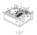
- FIG. 1 is an external perspective view of a SAW device according to a first embodiment of the present invention.
- FIG. 2 is a schematic perspective view showing the SAW device of FIG. 1 in a partially broken state.
- FIG. 3 is a cross-sectional view taken along line III-III in FIG. 2.
- FIG. 4 is an enlarged view of a region IV in FIG. 3. It is sectional drawing parallel to the main surface of a board
- substrate in the cover upper surface of the SAW apparatus of FIG. 6 (a) to 6 (d) are cross-sectional views illustrating a method for manufacturing the SAW device of FIG. 7 (a) to 7 (c) are cross-sectional views showing a continuation of FIG. 6 (d).
- 8 (a) to 8 (c) are sectional views showing a continuation of FIG.
- FIG. 10A is a cross-sectional view of the SAW device of the third embodiment
- FIG. 10B is an enlarged view of a region Xb in FIG.
- the symbols may be given uppercase alphabetic additional symbols such as “first terminal 7A to sixth terminal 7F” for the same or similar configurations. Further, in this case, the number at the beginning of the name and the above-described additional code, such as simply “terminal 7”, may be omitted.
- FIG. 1 is an external perspective view of a SAW device 1 according to the first embodiment of the present invention. However, illustration of an insulating layer 43 to be described later is omitted.
- the SAW device 1 is a so-called wafer level package (WLP) type SAW device.
- the SAW device 1 includes a substrate 3, a cover 5 fixed to the substrate 3, first terminals 7 ⁇ / b> A to 6 ⁇ / b> F exposed from the cover 5, and an upper surface of the cover 5 (surface opposite to the substrate 3).
- the laminated reinforcing layer 8 and the back surface portion 9 provided on the side opposite to the cover 5 of the substrate 3 are provided.
- the SAW device 1 is input with a signal via any one of the plurality of terminals 7.
- the input signal is filtered by the SAW device 1.
- the SAW device 1 outputs the filtered signal via any of the plurality of terminals 7.
- the SAW device 1 is, for example, resin-sealed in a state where the surface on the cover 5 side faces a mounting surface such as a circuit board (not shown) and is placed on the mounting surface, whereby the terminal 7 is placed on the mounting surface. It is mounted while connected to the terminal.
- the substrate 3 is constituted by a piezoelectric substrate.
- the substrate 3 is a rectangular parallelepiped single crystal substrate having piezoelectricity such as a lithium tantalate single crystal or a lithium niobate single crystal.
- substrate 3 has the 1st main surface 3a and the 2nd main surface 3b of the back side.
- the planar shape of the substrate 3 may be set as appropriate.
- the substrate 3 is a rectangle whose longitudinal direction is the Y direction.
- the size of the substrate 3 may be set as appropriate.
- the thickness is 0.2 to 0.5 mm, and the length of one side is 0.5 to 2 mm.
- the cover 5 is provided so as to cover the first main surface 3a.
- the planar shape of the cover 5 is, for example, the same as the planar shape of the substrate 3, and in the present embodiment, it is a rectangle having the Y direction as the longitudinal direction.
- the cover 5 has, for example, a width approximately equal to that of the first main surface 3a and covers almost the entire surface of the first main surface 3a.
- the cover 5 is made of a photosensitive resin.
- the photosensitive resin is, for example, a urethane acrylate-based, polyester acrylate-based, or epoxy acrylate-based resin that is cured by radical polymerization of an acryl group or a methacryl group.
- the plurality of terminals 7 are exposed from the upper surface of the cover 5.
- the number and arrangement positions of the plurality of terminals 7 are appropriately set according to the configuration of the electronic circuit inside the SAW device 1.
- six terminals 7 are arranged along the outer periphery of the cover 5.
- the reinforcing layer 8 is for reinforcing the strength of the cover 5.
- the reinforcing layer 8 is made of a material having a Young's modulus higher than that of the material constituting the cover 5.
- the cover 5 is made of resin, whereas the reinforcing layer 8 is made of metal.
- the Young's modulus of the cover 5 is 0.5 to 1 GPa, whereas the Young's modulus of the reinforcing layer 8 is 100 to 250 GPa.
- the thickness of the reinforcing layer 8 is, for example, 1 to 50 ⁇ m.
- the reinforcing layer 8 is formed over a relatively wide range of the cover 5.
- the cover 5 is formed over substantially the entire surface of the cover 5, avoiding the arrangement position of the terminals 7.
- the reinforcing layer 8 is not connected to the terminal 7 and is in an electrically floating state.
- the back surface portion 9 includes, for example, a back electrode that covers almost the entire surface of the second main surface 3b and an insulating protective layer that covers the back electrode.
- the charge charged on the surface of the substrate 3 due to a temperature change or the like is discharged by the back electrode. Damage to the substrate 3 is suppressed by the protective layer.
- illustration and description of the back surface part 9 may be omitted.
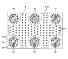
- FIG. 2 is a perspective view of the SAW device 1 with a part of the cover 5 cut away.
- the SAW element 11 is provided on the first main surface 3a.
- the SAW element 11 is for filtering a signal input to the SAW device 1.
- the SAW element 11 has a pair of comb-like electrodes (IDT electrodes) 15 formed on the first main surface 3a.
- Each comb-like electrode 15 includes a bus bar 15a extending in the propagation direction (X direction) of the surface acoustic wave on the substrate 3, and a plurality of electrode fingers 15b extending from the bus bar 15a in a direction (Y direction) perpendicular to the propagation direction.
- One comb-like electrode 15 is provided so that the electrode fingers 15b mesh with each other.
- FIG. 2 is a schematic diagram, a pair of comb-like electrodes 15 having several electrode fingers 15b is shown. In practice, a plurality of pairs of comb-like electrodes having a larger number of electrode fingers may be provided.
- a plurality of SAW elements 11 may be connected by a system such as a series connection or a parallel connection, and a ladder type SAW filter, a double mode SAW resonator filter, or the like may be configured.
- the SAW element 11 is made of an Al alloy such as an Al—Cu alloy.
- the cover 5 includes a frame portion 35 that surrounds the SAW element 11 in a plan view of the first main surface 3a, and a lid portion 37 that closes the opening of the frame portion 35.
- a vibration space 10 that facilitates vibration of the SAW element 11 is formed by a space surrounded by the first main surface 3a (strictly speaking, a protective layer 25 described later), the frame portion 35, and the lid portion 37.
- the vibration space 10 may be provided in an appropriate number and shape, and FIG. 2 illustrates the case where two vibration spaces 10 are provided.
- the frame portion 35 is configured by forming one or more openings (two in the present embodiment) serving as the vibration space 10 in a layer having a substantially constant thickness.
- the thickness of the frame part 35 (height of the vibration space 10) is, for example, several ⁇ m to 30 ⁇ m.
- the lid portion 37 is configured by a layer having a substantially constant thickness that is stacked on the frame portion 35.
- the thickness of the lid portion 37 is, for example, several ⁇ m to 30 ⁇ m.
- the frame part 35 and the lid part 37 may be formed of the same material, or may be formed of different materials. In the present application, for convenience of explanation, the boundary line between the frame portion 35 and the lid portion 37 is clearly shown. However, in an actual product, the frame portion 35 and the lid portion 37 are formed of the same material and are integrally formed. May be.
- the reinforcing layer 8 overlaps the vibration space 10 in a plan view of the first main surface 3a. More specifically, the reinforcing layer 8 covers the entire vibration space 10 and extends to the outside of the vibration space 10. Therefore, the reinforcing layer 8 is spanned over the frame portion 35 together with the lid portion 37 and is supported by the frame portion 35.
- the terminal 7 is provided upright on the first main surface 3a, as shown well in the sixth terminal 7F in FIG. 2, and the frame portion 35 and the lid portion 37 are directed in the direction in which the first main surface 3a faces. It penetrates and is exposed on the upper surface of the cover 5.
- the terminal 7 has a columnar portion 7a formed in a columnar shape and a flange 7b protruding from the side surface of the columnar portion 7a.
- the columnar portion 7 a penetrates the cover 5, and the flange 7 b is laminated on the upper surface of the cover 5.
- the upper end surface of the terminal 7 including the flange 7b constitutes a land 7c connected to a circuit board or the like.
- the columnar portion 7a is formed in a columnar shape, for example.
- the diameter of the columnar portion 7a is, for example, 20 to 120 ⁇ m.
- the flange 7b is formed over the entire circumference of the columnar portion 7a and has a substantially constant width. Therefore, the shape of the land 7c is a similar shape (circular in this embodiment) that is slightly larger than the cross-sectional shape parallel to the first main surface 3a of the columnar portion 7a.
- the diameter of the land 7c is larger than the diameter of the columnar portion 7a, for example, by a difference of 5 to 100 ⁇ m.
- the first main surface 3a is provided with a wiring 12 connected to the SAW element 11, and a first pad 13A to a sixth pad 13F (only part of which are shown in FIG. 2) connected to the wiring 12.
- the terminal 7 is connected to the SAW element 11 by being provided on the pad 13.
- FIG. 3 is a cross-sectional view taken along line III-III in FIG.
- FIG. 4 is an enlarged view of region IV in FIG.
- the SAW device 1 includes a conductive layer 19 provided on the first main surface 3a and a protective layer 25 stacked on the conductive layer 19 and the first main surface 3a. Further, the SAW device 1 includes a base layer 39 formed on the cover 5, a metal part 41 formed on the surface of the base layer 39, and an insulating layer 43 covering the metal part 41.
- the conductive layer 19 is a basic layer regarding the configuration of circuit elements, wirings, and the like on the first main surface 3a. Specifically, the conductive layer 19 constitutes the SAW element 11, the wiring 12 and the pad 13.
- the conductive layer 19 is made of, for example, an Al alloy such as an Al—Cu alloy, and the thickness thereof is, for example, 100 to 300 nm.
- the protective layer 25 contributes to the oxidation prevention of the SAW element 11 and the like.
- the protective layer 25 is made of, for example, silicon oxide (such as SiO 2 ), aluminum oxide, zinc oxide, titanium oxide, silicon nitride, or silicon.
- the thickness of the protective layer 25 is, for example, about 1/10 (10 to 30 nm) of the thickness of the conductive layer 19.
- the protective layer 25 is formed over the entire first main surface 3a except for the position where the pad 13 is disposed.
- the cover 5 is laminated on the protective layer 25.
- the base layer 39 constitutes a portion in contact with the cover 5 and the pad 13 of the terminal 7 and a portion in contact with the cover 5 of the reinforcing layer 8.
- the underlayer 39 is made of, for example, copper or titanium.
- the thickness of the foundation layer 39 is substantially uniform. The thickness may be set as appropriate. For example, when the underlayer 39 is made of copper, it is 300 nm to 1 ⁇ m, and when the underlayer 39 is made of titanium, it is 10 to 100 nm.
- the metal part 41 constitutes the inner side part of the columnar part 7a and the upper part (the side opposite to the cover 5) of the flange 7b in the terminal 7. Further, the metal part 41 constitutes an upper part of the reinforcing layer 8.
- the metal part 41 is made of, for example, copper.
- the insulating layer 43 covers the entire surface of the reinforcing layer 8.
- the insulating layer 43 is also formed from the edge of the reinforcing layer 8 to the edge of the land 7 c of the terminal 7.
- the insulating layer 43 contributes to the insulation of the reinforcing layer 8, and also contributes to suppressing moisture and the like from entering the gap between the terminal 7 and the cover 5.
- the insulating layer 43 may be made of, for example, an epoxy resin that is generally used as a solder resist.
- the insulating layer 43 may be made of an inorganic material having a higher water shielding property than an organic material. Examples of the inorganic material include silicon oxide (such as SiO 2 ), silicon nitride, and silicon.
- the thickness of the insulating layer 43 is, for example, 500 nm to 20 ⁇ m.
- the insulating layer 43 only needs to be formed so as to cover at least either the side surface of the reinforcing layer 8 or the side surface of the land 7c.
- a plurality of first protrusions 31 protrude from the surface of the reinforcing layer 8 on the cover 5 side.
- a second protrusion 33 protrudes from the surface of the flange 7b of the terminal 7 on the cover 5 side.
- the first protruding portion 31 and the second protruding portion 33 are also configured by the base layer 39 and the metal portion 41. Accordingly, the first protrusion 31 is formed integrally with the reinforcing layer 8, and the second protrusion 33 is formed integrally with the terminal 7.
- first protrusion 31 can be regarded as a part of the reinforcing layer 8 and the second protrusion 33 can be regarded as a part of the terminal 7.
- the part 31 and the second protrusion 33 will be described as parts separate from the reinforcing layer 8 and the terminal 7.
- the first protrusion 31 and the second protrusion 33 protrude into the cover 5, and the side surfaces thereof are covered with the cover 5.
- the first protrusion 31 and the second protrusion 33 are fitted in the recesses corresponding to the shapes of the protrusions provided on the upper surface of the cover 5.
- the height (protrusion height) of the protruding portion of the first protruding portion 31 and the second protruding portion 33 from the reinforcing layer 8 is the thickness of the lid portion 37 (the thickness from the ceiling of the vibration space 10 to the upper surface of the cover 5). ),
- the first protrusion 31 and the second protrusion 33 do not penetrate the cover 5, and the front end surfaces thereof are covered with the cover 5.
- the projecting heights of the first projecting portion 31 and the second projecting portion 33 are, for example, 3 to 20 ⁇ m, 10 to 70% of the thickness of the lid portion 37, or the thickness of the base layer 39 or more.
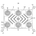
- FIG. 5 is a cross-sectional view of the SAW device 1 parallel to the first main surface 3 a on the upper surface of the cover 5.
- the shapes of the reinforcing layer 8 and the flange 7b are also indicated by a two-dot chain line.
- the plurality of first protrusions 31 are scattered in a plan view of the first main surface 3a. That is, in the plan view of the first main surface 3a, the plurality of first protrusions 31 have shapes and sizes that can be regarded as points with respect to the width of the cover 5, such as a circle, an ellipse, or a polygon. Formed and distributed over the cover 5.
- the cross-sectional shape parallel to the first main surface 3a of the plurality of first protrusions 31, the cross-sectional area and the density may be set as appropriate.
- the plurality of first protrusions 31 are formed in a circular shape having the same diameter, and are distributed so that the density is uniform over the entire surface of the reinforcing layer 8.
- the circular diameter is, for example, 3 to 20 ⁇ m.
- the total cross-sectional area of the plurality of first protrusions 31 is, for example, 10 to 70% of the area of the reinforcing layer 8.
- the second protrusion 33 is formed in a line shape (protrusion) surrounding the columnar portion 7a of the terminal 7 in a plan view of the first main surface 3a. Specifically, the second protrusion 33 is formed in a circular shape concentric with the columnar portion 7a. For example, the second protrusion 33 is formed so that the distance from the columnar portion 7a is 10 to 45 ⁇ m.
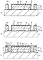
- FIG. 6 (a) to 8 (c) are cross-sectional views corresponding to FIG. 3 (III-III line in FIG. 2) for explaining a method of manufacturing the SAW device 1.
- FIG. The manufacturing process proceeds in order from FIG. 6 (a) to FIG. 8 (c).
- the steps described below are realized in a so-called wafer process. That is, a thin film formation, a photolithography method, or the like is performed on the mother substrate that becomes the substrate 3 by being divided, and then a large number of SAW devices 1 are formed in parallel by dicing. . However, in FIGS. 6A to 8C, only a portion corresponding to one SAW device 1 is shown. In addition, although the shape of the conductive layer and the insulating layer changes with the progress of the process, a common code is used before and after the change.
- a conductive layer 19 is formed on the first main surface 3a of the substrate 3.
- a metal layer to be the conductive layer 19 is formed on the first main surface 3a by a thin film forming method such as a sputtering method, a vapor deposition method, or a CVD (Chemical Vapor Deposition) method.
- the metal layer is patterned by a photolithography method using a reduction projection exposure machine (stepper) and an RIE (Reactive (Ion Etching) apparatus. By patterning, the SAW element 11, the wiring 12, and the pad 13 are formed. That is, the conductive layer 19 is formed.
- a protective layer 25 is formed as shown in FIG. Specifically, first, a thin film to be the protective layer 25 is formed by an appropriate thin film forming method.
- the thin film forming method is, for example, a sputtering method or a CVD method.
- a part of the thin film is removed by a photolithography method so that a portion of the conductive layer 19 constituting the pad 13 is exposed. Thereby, the protective layer 25 is formed.
- a thin film that becomes the frame portion 35 is formed as shown in FIG.
- the thin film is formed, for example, by attaching a film formed of a photosensitive resin or by a thin film forming method similar to that for the protective layer 25.
- the thin film to be the frame portion 35 is formed, as shown in FIG. 6D, a part of the thin film is removed by a photolithography method or the like, and the opening and the terminal 7 constituting the vibration space 10 are arranged. A predetermined hole 35h is formed. The thin film is also removed with a constant width on the dicing line. In this way, the frame portion 35 is formed.
- the lid portion 37 (strictly, the lid before the concave portion in which the first protrusion 31 and the second protrusion 33 are embedded is formed. Part) is formed. Specifically, first, a thin film that becomes the lid portion 37 is formed. The thin film is formed, for example, by attaching a photosensitive resin film. When the thin film is formed, the opening of the frame portion 35 is closed, and the vibration space 10 is configured. In the thin film, a portion on the hole 35h (FIG. 6D) is removed by a photolithography method or the like, and a hole 5h (including the hole 35h) where the terminal 7 is to be disposed is formed. The thin film is also removed with a constant width on the dicing line. In this way, the lid portion 37 is formed.
- a mask 51 is formed as shown in FIG.
- the mask 51 is formed so that the upper surface of the cover 5 is exposed at a position where the first protrusion 31 and the second protrusion 33 are to be disposed.
- the mask 51 is formed, for example, by forming a photosensitive resin thin film by spin coating or the like and patterning the thin film by photolithography.
- the mask 51 is removed and the base layer 39 is formed as shown in FIG.
- the underlayer 39 is formed over the entire top surface of the cover 5.
- the underlayer 39 is also formed on the inner peripheral surface and the bottom surface of the hole 5h, the first recess 37a, and the second recess 37b.
- the underlayer 39 is formed by, for example, a sputtering method.
- a resist layer 53 is formed as shown in FIG.
- the resist layer 53 is formed so that the foundation layer 39 is exposed in a range where the land 7c and the reinforcing layer 8 are to be disposed.
- the resist layer 53 is formed, for example, by forming a photosensitive resin thin film by spin coating or the like and patterning the thin film by photolithography.
- the resist layer 53 is formed, as shown in FIG. 8C, metal is deposited on the exposed portion of the base layer 39 by electroplating, and the first metal is deposited on the first recess 37a and the second recess 37b. Then, the second metal is laminated on the upper surface of the cover 5. As a result, the metal portion 41 made of the first metal and the second metal is formed. Then, the portion of the base layer 39 covered with the resist layer 53 and the resist layer 53 are removed. As a result, the reinforcing layer 8, the terminal 7, the first protrusion 31, and the second protrusion 33 including the base layer 39 and the metal portion 41 are formed. Thereafter, although not particularly shown, the insulating layer 43 is formed by photolithography or the like.
- the SAW device 1 includes the substrate 3, the SAW element 11 provided on the first main surface 3 a of the substrate 3, and the first main surface 3 a, and the vibration space on the SAW element 11. 10 and a cover 5 that forms 10.
- the SAW device 1 is formed integrally with the conductor layer (the reinforcing layer 8 or the flange 7b) formed on the upper surface of the cover 5, and protrudes from the conductor layer into the cover 5, and includes a front end surface and side surfaces. Has the first protrusion 31 or the second protrusion 33 covered with the cover 5.
- the conductor layer (the reinforcing layer 8 or the flange 7b) has a large area in contact with the cover 5 due to the formation of the first protrusion 31 or the second protrusion 33, and the peeling of the conductor layer is suppressed.
- a layer having a thermal expansion coefficient intermediate between these thermal expansion coefficients is formed between the conductor layer (metal) and the cover 5 (resin), and the thermal expansion difference is alleviated. , Peeling of the conductor layer is suppressed.
- the thermal expansion coefficient of the conductor layer (Cu) is about 13 ppm / K
- the thermal expansion coefficient of the cover 5 (resin) is about -35 ppm / K.
- the suppression of peeling due to the difference in thermal expansion can also be considered as follows.
- the cover 5 tends to shrink toward the center and the reinforcing layer 8 tends to expand toward the outer periphery. Therefore, the cover 5 is shifted in the direction indicated by the arrow y11 with respect to the reinforcing layer 8 due to the difference in thermal expansion between the cover 5 and the reinforcing layer 8.
- the 1st protrusion 31 protrudes inside the cover 5, as shown by arrow y13, the force which latches the cover 5 can be exhibited. As a result, the occurrence of displacement between the reinforcing layer 8 and the cover 5 is suppressed, and peeling of the reinforcing layer 8 is suppressed.
- the protrusion height of the first protrusion 31 is smaller than the thickness from the ceiling of the vibration space 10 to the upper surface of the cover 5. Therefore, the conductor layer that overlaps the vibration space 10 like the reinforcing layer 8 can be suitably prevented from peeling without affecting the hermeticity of the vibration space 10.
- An example of the conductor layer is a reinforcing layer 8 that is made of a material (metal) that overlaps the vibration space 10 and has a higher Young's modulus than the material (resin) that forms the cover 5.
- the first protrusion 31 improves the integrity of the reinforcing layer 8 and the lid portion 37, thereby enhancing the effect of reinforcing the lid portion 37 by the reinforcing layer 8.
- a plurality of the first protrusions 31 are provided in a scattered manner in the plan view of the first main surface 3a.
- the area of the first protrusion 31 in contact with the cover 5 is relatively larger than the volume of the first protrusion 31 compared to the second embodiment described later, and the reinforcing layer 8 is effectively formed. Peeling can be suppressed.
- the plurality of first protrusions 31 are each formed in a circular shape in a plan view of the first main surface 3 a and are distributed at a uniform density over the entire reinforcing layer 8. Therefore, the effects of increasing the contact area and reducing the difference in thermal expansion described above can be obtained over the entire reinforcing layer 8 and in all directions, and the peeling of the reinforcing layer 8 is preferably suppressed. It is expected.
- the SAW device 1 further has a terminal 7 connected to the SAW element 11.
- the terminal 7 is provided upright on the first main surface 3 a, and includes a columnar portion 7 a that penetrates the cover 5, and a flange 7 b that protrudes from the side surface of the columnar portion 7 a and is laminated on the upper surface of the lid portion 37.
- An example of the conductor layer is a flange 7b. Therefore, the peeling of the flange 7b by the second protrusion 33 is suppressed, so that moisture and the like are suppressed from entering the gap between the columnar portion 7a and the hole 5h from between the cover 5 and the flange 7b. As a result, corrosion of the pad 13 and the like is suppressed.
- the terminal 7 may be subjected to a force to be pulled out from the cover 5 such as being connected to another circuit board, but the resistance of the terminal 7 to such pulling out is also improved.
- the second protrusion 33 surrounds the columnar portion 7a in the plan view of the first main surface 3a. Therefore, as indicated by an arrow y1 in FIG. 4, the creepage distance from the edge of the flange 7b to the hole 5h is longer than when the second protrusion 33 is not provided. As a result, the entry of moisture into the gap between the columnar portion 7a and the hole 5h is more effectively suppressed.
- the manufacturing method of the SAW device 1 of the present embodiment includes the following steps.
- a step of forming the SAW element 11 on the first main surface 3a of the substrate 3 (FIG. 6A).
- a photosensitive resin layer that covers the SAW element 11 is laminated, the photosensitive resin layer is exposed and developed, and the cover 5 that forms the vibration space 10 is formed on the SAW element 11 by the developed photosensitive resin layer.
- FIG. 6 (c) to FIG. 7 (a) Step of forming mask 51 on the upper surface of cover 5 and etching the upper surface of cover 5 through mask 51 to form first recess 37a or second recess 37b (FIGS. 7B and 7C) .
- the metal is laminated on the upper surface of the cover 5 while filling the first concave portion 37a or the second concave portion 37b with the metal, and the conductor layer (the reinforcing layer 8 or the flange 7b) laminated on the upper surface of the cover 5 and the conductor layer in the cover 5 A step of forming the first protrusion 31 or the second protrusion 33 projecting to the right (FIGS. 8A to 8C).
- the first concave portion 37a or the second concave portion 37b is formed by an etching process separate from the process of exposing and developing the cover 5, whereby the vibrating space 10 and the cover penetrating the frame portion 35 are formed.
- the first concave portion 37a or the second concave portion 37b that does not penetrate the lid portion 37 can be easily formed while the hole portion 5h penetrating the through portion 5 is simply formed.
- the 1st protrusion 31 or the 2nd protrusion 33 whose protrusion amount is smaller than the thickness of the cover part 37 can be formed easily.
- the SAW device 1 is an example of the acoustic wave device of the present invention
- the SAW element 11 is an example of the acoustic wave device of the present invention.
- FIG. 9 is a cross-sectional view corresponding to FIG. 5 of the SAW device 101 of the second embodiment.
- the same or similar configurations as those in the first embodiment are denoted by the same reference numerals as those in the first embodiment, and description thereof is omitted.
- the SAW device 101 of the second embodiment is different from the SAW device 1 of the first embodiment only in the configuration of the first protrusion 131.
- the 1st protrusion 131 is formed in the linear form (projection) in planar view of the 1st main surface 3a.
- a plurality of first protrusions 131 are formed in a straight line.
- the plurality of first protrusions 131 extend in a shape surrounding the central side of the reinforcing layer 8 (lid portion 37) in a multiple manner in the plan view of the first main surface 3a.
- the some 1st protrusion 131 may be connected to the other 1st protrusion 131 in the edge part etc., and does not need to be connected.
- the protrusion height and width of the first protrusion 131 may be the same as the protrusion height and diameter of the first protrusion 31 of the first embodiment.
- the first protrusion 131 provides the effect of suppressing the peeling of the reinforcing layer 8.
- the first protrusion 131 is formed in a linear shape in the plan view of the first main surface 3a, it functions like a beam and contributes to an improvement in the bending rigidity of the reinforcing layer 8. As a result, the reinforcing effect of the lid portion 37 by the reinforcing layer 8 is enhanced.
- a force is applied to the cover 5 so as to displace the cover 5 with respect to the reinforcing layer 8.
- the force for shifting the cover 5 with respect to the reinforcing layer 8 is the outer peripheral side of the cover 5 (reinforcing layer 8) as shown by an arrow y11 in FIG. Work from the center side.
- the linear first protrusion 131 extends in a shape surrounding the central side of the lid portion 37 in a multiple manner in a plan view of the first main surface 3a. Therefore, the first protrusion 131 blocks the force for shifting the cover 5 with respect to the reinforcing layer 8 as compared with the protrusions of other shapes such as the first protrusion 31 of the first embodiment. Cheap. As a result, in the second embodiment, peeling of the reinforcing layer 8 from the cover 5 is effectively suppressed.
- FIG. 10A is a cross-sectional view corresponding to FIG. 5 of the SAW device 201 of the third embodiment.
- FIG. 10B is an enlarged view of the region Xb in FIG.
- the first protrusion 31 and the second protrusion 33 of the first embodiment are not provided.
- the upper surface of the cover 205 (lid portion 237) is roughened. That is, minute irregularities are formed on the upper surface of the cover 205.
- the lower surface of the base layer 39 has a shape corresponding to the unevenness of the upper surface of the cover 205 and is in close contact with the upper surface of the cover 205.
- the area where the conductor layer (the reinforcing layer 8 or the flange 7b) and the cover 205 are in contact with each other is increased, thereby suppressing the peeling of the conductor layer from the cover 205. Is done.
- the arithmetic average roughness (arithmetic surface roughness when measured with a laser microscope) of the upper surface of the roughened cover 205 is, for example, 0.5 ⁇ m or more and 2 ⁇ m or less.
- the roughening of the arithmetic average roughness is effective, for example, when the thickness of the cover 205 is 10 ⁇ m or more and 80 ⁇ m or less and / or when the thickness of the conductor layer is 10 ⁇ m or more and 50 ⁇ m or less.
- the upper surface of the lid portion 237 of the SAW device 201 has a higher oxygen atom content than the upper surface of the lid portion 37 of the first embodiment.
- the upper surface of the lid portion 237 has a higher oxygen atom content than the lower surface (the surface that is in close contact with the frame portion 35 and the surface that is the ceiling of the vibration space 10).
- oxygen atom content is measured in the range of several nm to several tens of nm from the upper surface or the lower surface of the lid 237 by, for example, X-ray photoelectron spectroscopy (XPS) analysis.
- XPS X-ray photoelectron spectroscopy
- the lid portion 237 includes a lower surface side portion 237c including the lower surface of the lid portion 237, and an upper surface side portion 237d including the upper surface of the lid portion 237 and having a higher oxygen content than the lower surface side portion 237c.
- the boundary between the lower surface side portion 237c and the upper surface side portion 237d is not necessarily clear (there is no need to have a boundary where the oxygen atom content rate changes abruptly).
- the underlayer 39 is preferably a metal that easily forms an oxide such as Ti.
- FIG. 11 is a flowchart showing a procedure of a method for manufacturing the SAW device 201.
- FIG. 11 mainly shows the difference from the method of manufacturing the SAW device 1 according to the first embodiment described with reference to FIGS. 6 to 8, and the parts common to the method of manufacturing the SAW device 1 are shown. Most are omitted.
- step S1 corresponds to the processing in FIG. 6D, and the same processing as in the first embodiment is performed until this processing.
- step S2 (plasma) ashing processing is performed. That is, the first main surface 3a side of the substrate 3 is exposed to oxygen plasma. Thereby, the residue of the photoresist (the portion where the frame portion 35 is removed) is removed. That is, the descum process is performed.
- step S3 corresponds to the process of FIG. 7A, and the formation of a thin film to be the lid 237 and the removal of a part thereof are performed.
- step S4 although description is omitted in the first embodiment, (post) baking (bake) of the cover 205 is performed.
- the baking temperature is a temperature at which the resin of the cover 205 is polymerized. As a result, the remaining solvent and moisture are removed, and the adhesion between the cover 205 and the substrate 3 is improved. Note that the baking temperature and time are appropriately set according to the material of the cover 205.
- step S5 (plasma) ashing processing is performed as in step S2. However, in step S5, ashing is performed after the baking in step S4. As a result, in step S5, in addition to removing the residue, the surface of the cover 205 is also roughened.
- the resin of the cover 205 is exposed to oxygen plasma, whereby the resin and oxygen are combined to form an oxygen substituent.
- the upper surface of the cover 205 (lid portion 237) is a surface of the cover 205 that is not exposed to oxygen plasma (for example, a surface that is in close contact with the frame portion 35 of the lid portion 237 and a ceiling that is the ceiling of the vibration space 10 of the lid portion 237).
- the oxygen atom content is increased.
- step S6 corresponds to the process of FIG. After this process, the same process as in the second embodiment is performed.
- the process (process of FIG.7 (b) and FIG.7 (c)) for forming the 1st protrusion 31 and the 2nd protrusion 33 is not performed in 3rd Embodiment.
- the upper surface of the cover 205 can be roughened, the oxygen atom content on the upper surface of the cover 205 can be increased, and the descum in the cover 205 can be performed simultaneously.
- the manufacturing process can be shortened. Further, since the conductor layer (reinforcing layer 8 or the like) is formed after the cover 205 is cleaned by the descum, the peeling of the conductor layer from the cover 205 is further suppressed.
- Ashing conditions may be set as appropriate. In general, the larger the pressure of oxygen plasma, the greater the power applied to the oxygen plasma, and the longer the time that the cover 205 is exposed to oxygen plasma, the more the surface of the cover 205 is scraped and roughened. Progress.
- Example 2 A SAW device according to the third embodiment and a sample simulating the SAW device were prepared, and performance evaluation was performed. Specifically, it is as follows.
- Ashing condition of sample for peel strength evaluation Pressure 11 Pa or 73 Pa Power (power): 100W Time: 30 minutes
- a sample that was not subjected to ashing was also prepared.
- two samples were prepared for each of the sample that was not subjected to ashing, the sample that was subjected to ashing at a pressure of 11 Pa, and the sample that was subjected to ashing at a pressure of 73 Pa. That is, a total of six samples were prepared.
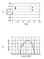
- FIG. 12 (a) is a diagram showing the evaluation results.
- the horizontal axis represents the ashing pressure P
- the vertical axis represents the peel strength St.
- the peel strength when the ashing process is performed shows a value that is about twice the peel strength when the ashing process is not performed. In the range of this example, no significant difference in peel strength due to the difference in ashing pressure was observed.
- the change in the height difference of the upper surface of the cover 205 at this time was as follows.
- the height difference is mainly caused by a gentle curve on the upper surface of the cover 205 and is different from the roughness of the rough surface.
- the amount of reduction in the thickness of the cover 205 by ashing was 0.5 to 1 ⁇ m. Therefore, it has been confirmed that there is no problem in forming the SAW device having the cover 205 having a thickness of 10 ⁇ m or more (preferably 55 to 60 ⁇ m).
- FIG. 12B is a diagram comparing the electrical characteristics of the comparative example with the electrical characteristics of the SAW device of the third embodiment.
- the horizontal axis indicates the frequency, and the vertical axis indicates the insertion loss.
- the SAW device of the comparative example is manufactured by a manufacturing method that excludes the ashing process from the manufacturing method of the third embodiment.
- the present invention is not limited to the above embodiment, and may be implemented in various modes.
- the roughening of the third embodiment is applied to the first or second embodiment, and an elastic wave device in which a protrusion protruding from the conductor layer is provided and the upper surface of the cover is roughened is implemented. May be.
- the elastic wave device is not limited to a SAW device.
- the acoustic wave device may be a piezoelectric thin film resonator or a boundary acoustic wave device (however, included in a broad sense SAW device).
- the boundary acoustic wave device includes a piezoelectric substrate, an acoustic wave element located on the principal surface of the piezoelectric substrate, and a medium layer located on the acoustic wave element, and includes a principal surface of the piezoelectric substrate and the medium layer.
- An elastic boundary wave (included in a broad sense SAW) propagates through the boundary.
- the cover may also serve as the medium layer. In other words, the vibration space may not be provided.
- the protective layer (25) may be omitted, or conversely, other appropriate layers may be formed.
- a wiring that three-dimensionally intersects with the wiring 12 via an insulator may be provided, or a connection reinforcing layer that is interposed between the pad 13 and the terminal 7 and reinforces the adhesive force between the pad 13 and the terminal 7. It may be provided, or a conductive layer may be provided between the frame portion and the lid portion.
- the conductor layer formed on the upper surface of the cover is not limited to the reinforcing layer or the terminal flange.
- the conductor layer may constitute a circuit such as an inductor, a capacitor, or a wiring.
- the reinforcing layer may be connected to a terminal to which a reference potential is applied.
- the reinforcing layer is not limited to one wider than the vibration space.
- the reinforcing layer may have the same shape as the vibration space, or may have a size that fits in the vibration space. Further, in the case where the reinforcing layer is wider than the vibration space, the reinforcing layer may not overlap with the frame portion on the entire circumference of the vibration space.
- the protrusion whose tip surface is covered by the cover is not limited to a protrusion whose protrusion is smaller than the thickness of the lid.
- the protrusion provided on the outer peripheral side of the vibration space may penetrate the entire lid portion, and the tip end surface may be covered by the upper surface of the frame portion, or the entire lid portion and a part of the frame portion may be covered. It penetrates and the front end surface may be covered with the frame part.
- the protrusions scattered in the reinforcing layer may be formed so that the density is high at a position where the reinforcing layer is easily peeled off.
- the line-shaped protrusion provided on the reinforcing layer is not limited to the one surrounding the central side of the reinforcing layer.
- the line-shaped protrusion may be formed in a net shape.
- a line-shaped protrusion surrounds the center side of a reinforcement layer, a line-shaped protrusion is not limited to a straight line, A curve may be sufficient.
- a plurality of line-shaped protrusions may be provided concentrically around the center side of the reinforcing layer, or a single line-shaped protrusion may be provided in a spiral shape surrounding the center side of the reinforcing layer. Good.
- the protrusion (33) provided on the terminal flange is not limited to the one provided in an annular shape.
- the protrusions provided on the flange may be interspersed like the protrusions (31) of the reinforcing layer in the first embodiment, or may be a line extending radially.
- the terminal having the columnar portion penetrating the cover may not be provided.
- the protrusion is not covered by the cover. Good. That is, the protrusion may penetrate the lid portion and the frame portion and reach the main surface.
- the elastic wave devices according to the first and second aspects are common in that a protrusion protruding from the conductor layer into the cover is provided to suppress peeling of the conductor layer laminated on the cover. It has technical characteristics. What is described separately in the first and second viewpoints is merely the convenience of expression for eliminating that the columnar portion of the terminal having the columnar portion and the flange is included in the protrusion.
- the terminal columnar portion is the main body portion of the terminal, and the flange is added to the columnar portion in order to expand the land area, so the terminal columnar portion suppresses the flange from coming off. It is not provided for this purpose and is essentially different from the protrusions of the present invention.
- the site where the oxygen atom content rate is compared with the upper surface of the cover may be the lower surface of the resin layer (in the embodiment, the lid portion 237) constituting the upper surface of the cover, and vibration It is not limited to the surface constituting the ceiling of the space.
- the site where the oxygen atom content rate is compared with the upper surface of the cover may be the lower surface of the resin layer (in the embodiment, the lid portion 237) constituting the upper surface of the cover, and vibration It is not limited to the surface constituting the ceiling of the space.
- the site where the oxygen atom content rate is compared with the upper surface of the cover may be the lower surface of the resin layer (in the embodiment, the lid portion 237) constituting the upper surface of the cover, and vibration It is not limited to the surface constituting the ceiling of the space.
- oxygen atoms are formed between the upper surface and the lower surface of the resin layer (the surfaces that are in close contact with the main surface of the piezoelectric substrate). The content of may be compared.
- the method of manufacturing the elastic wave device having the protrusions is not limited to a method of etching the upper surface of the cover separately from the development of the cover.
- a recess that accommodates the protrusion may be formed in the development of the lid.
- SYMBOLS 1 Surface acoustic wave apparatus (elastic wave apparatus), 3 ... Board
- SAW element elastic wave element
Landscapes
- Physics & Mathematics (AREA)
- Acoustics & Sound (AREA)
- Surface Acoustic Wave Elements And Circuit Networks Thereof (AREA)
Abstract
Description
(SAW装置の構成)
図1は、本発明の第1の実施形態に係るSAW装置1の外観斜視図である。ただし、後述する絶縁層43については図示を省略している。
図6(a)~図8(c)は、SAW装置1の製造方法を説明する、図3(図2のIII-III線)に対応する断面図である。製造工程は、図6(a)から図8(c)まで順に進んでいく。
図9は、第2の実施形態のSAW装置101の図5に相当する断面図である。なお、第2の実施形態以降において、第1の実施形態と共通または類似する構成については、第1の実施形態と同様の符号を付して説明を省略する。
図10(a)は、第3の実施形態のSAW装置201の図5に相当する断面図である。図10(b)は、図10(a)の領域Xbの拡大図である。
第3の実施形態のSAW装置および当該SAW装置を模した試料を作製し、性能評価を行った。具体的には以下のとおりである。
第3の実施形態のSAW装置を模した試料を形成し、SAICAS(Surface And Interfacial Cutting Analysis System)試験によって剥離強度を評価した。具体的には以下のとおりである。
試料は、以下に列挙する層がその列挙順に下から積層された積層体とした。なお、( )内は、実施形態のSAW装置の対応する部材の符号を示している。また、各層は、パターニングがなされない(下層の全面に形成された)、いわゆるベタ膜とした。
基板(3):LiTaO3からなる4インチのウェハ
導電層(19:11、12、13):Al-Cu合金
保護層(25):SiO2
樹脂層(205):エポキシ樹脂
下地層(39):Ti層(厚さ1500Å)およびその上のCu層(厚さ10500Å)
圧力:11Paまたは73Pa
パワー(電力):100W
時間:30分
なお、アッシング処理が行われない試料も用意した。また、アッシング処理が行われない試料、圧力11Paでアッシング処理が行われた試料、圧力73Paでアッシング処理が行われた試料のそれぞれについて、2つの試料を用意した。すなわち、合計6つの試料を用意した。
切刃によって下地層を削り取り、そのときの切刃に係る荷重を測定するSAICAS試験を採用した。具体的な条件は以下のとおりである。
装置:ダイプラ・ウィンテス社製「SAICAS NN-04型」
最大垂直可動距離:50μm
最大水平可動距離:500μm
剥離条件:刃幅0.3mm、垂直速度25nm/sec
水平速度:250nm/sec 定荷重モード
切刃に加えられた水平方向の荷重の平均値を切刃の幅で除算したものを剥離強度の評価指標とした。
以下の条件でアッシングを行って第3の実施形態に係るSAW装置を作製した。
圧力:163Pa
パワー(電力):100W
時間:30分
ベーク(ステップS4)後:4.96μm
アッシング(ステップS5)後:5.12μm
この結果から、アッシングを行っても高低差に大きな変化はないことが確認された。
以下の条件でアッシングを行って第3の実施形態に係るSAW装置を作製した。
圧力:73Pa
パワー(電力):100W
時間:30分
図12(b)は、比較例の電気特性と、第3の実施形態のSAW装置の電気特性とを比較する図である。横軸は、周波数を示し、縦軸は、挿入損失を示している。比較例のSAW装置は、第3の実施形態の製造方法からアッシング処理を除いた製造方法によって作製されたものである。
Claims (12)
- 基板と、
該基板の主面上に位置する弾性波素子と、
該弾性波素子上に位置し、上面に複数の凹部を有するカバーと、
複数の突部を有し、前記複数の突部が前記複数の凹部に嵌まった状態で前記カバーの上面に積層されている導体層と
を有する弾性波装置。 - 前記カバーは、前記基板の主面に位置し、平面視において前記弾性波素子を取り囲む環状の枠部と、該枠部の開口部を塞ぐ蓋部とをさらに有しており、
前記複数の突部の突出高さは、前記蓋部の厚みよりも小さい
請求項1に記載の弾性波装置。 - 前記導体層は、平面透視において前記枠部の開口部と重なる部分を有するとともに、前記導体層を構成する材料のヤング率は前記カバーを構成する材料のヤング率よりも高い
請求項2に記載の弾性波装置。 - 前記複数の突部は、前記導体層の表面に点在している
請求項3に記載の弾性波装置。 - 前記複数の突部は、前記導体層の全体に亘って一様な密度で分布している
請求項4に記載の弾性波装置。 - 前記複数の突部は、平面視における形状がそれぞれ線状である
請求項3に記載の弾性波装置。 - 前記弾性波素子に接続された端子をさらに有し、
該端子は、
前記主面上に位置し、前記カバーを貫通する柱状部と、
該柱状部の側面から突出して前記カバーの上面に重なっているフランジと
を有し、
前記導体層は、前記フランジである
請求項1または2に記載の弾性波装置。 - 前記複数の突部は、前記主面の平面視において、前記柱状部を囲んでいる
請求項7に記載の弾性波装置。 - 基板と、
該基板の主面上に位置する弾性波素子と、
前記基板の主面上に位置し、前記弾性波素子に接続されたパッドと、
前記弾性波素子上に位置し、上面に複数の凹部を有するカバーと、
前記パッド上に位置し、前記カバーを貫通する柱状部を有する端子と、
複数の突部を有し、前記複数の突部が前記複数の凹部に嵌まった状態で前記カバーの上面に積層されている導体層と
を有する弾性波装置。 - 基板の主面に弾性波素子を形成する工程と、
前記弾性波素子を感光性樹脂層で覆う工程と、
前記感光性樹脂層を露光する工程と、
露光された前記感光性樹脂層を現像する工程と、
現像された前記感光性樹脂層の上面にマスクを形成する工程と、
前記マスクが形成された前記感光性樹脂層の上面のうち前記マスクが形成されていない部位を凹状にエッチングする工程と、
エッチングされた凹状の部位に第1金属を充填する工程と、
前記感光性樹脂層の上面に第2金属を積層する工程と
を有する弾性波装置の製造方法。 - 前記感光性樹脂で覆う工程は、
前記基板の主面に形成された弾性波素子を保護層で被覆する工程と、
前記弾性波素子を前記保護層を介して前記感光性樹脂層で覆う工程と
を有する請求項10に記載の弾性波装置の製造方法。 - 基板の主面に弾性波素子を形成する工程と、
前記弾性波素子を感光性樹脂層で覆う工程と、
前記感光性樹脂層を露光する工程と、
露光された前記感光性樹脂層を現像する工程と、
現像された前記感光性樹脂層を該感光性樹脂層が重合する温度で加熱する工程と、
加熱された前記感光性樹脂層に酸素プラズマ処理を施す工程と、
前記酸素プラズマ処理された前記感光性樹脂層の上面に金属を積層する工程と
を有する弾性波装置の製造方法。
Priority Applications (2)
| Application Number | Priority Date | Filing Date | Title |
|---|---|---|---|
| JP2012512780A JP5514898B2 (ja) | 2010-04-27 | 2011-04-18 | 弾性波装置およびその製造方法 |
| CN201180016220.8A CN102823131B (zh) | 2010-04-27 | 2011-04-18 | 弹性波装置及其制造方法 |
Applications Claiming Priority (2)
| Application Number | Priority Date | Filing Date | Title |
|---|---|---|---|
| JP2010-102442 | 2010-04-27 | ||
| JP2010102442 | 2010-04-27 |
Publications (1)
| Publication Number | Publication Date |
|---|---|
| WO2011136070A1 true WO2011136070A1 (ja) | 2011-11-03 |
Family
ID=44861377
Family Applications (1)
| Application Number | Title | Priority Date | Filing Date |
|---|---|---|---|
| PCT/JP2011/059529 Ceased WO2011136070A1 (ja) | 2010-04-27 | 2011-04-18 | 弾性波装置およびその製造方法 |
Country Status (3)
| Country | Link |
|---|---|
| JP (1) | JP5514898B2 (ja) |
| CN (1) | CN102823131B (ja) |
| WO (1) | WO2011136070A1 (ja) |
Cited By (5)
| Publication number | Priority date | Publication date | Assignee | Title |
|---|---|---|---|---|
| WO2013121866A1 (ja) * | 2012-02-14 | 2013-08-22 | 株式会社村田製作所 | 電子部品素子およびそれを備えた複合モジュール |
| JP2015088653A (ja) * | 2013-10-31 | 2015-05-07 | 三菱電機株式会社 | 半導体装置 |
| JP5886989B1 (ja) * | 2015-01-13 | 2016-03-16 | ワイソル株式会社 | 圧電素子デバイス |
| JP2017228811A (ja) * | 2017-10-10 | 2017-12-28 | 三菱電機株式会社 | 半導体装置 |
| KR20220005253A (ko) * | 2020-07-06 | 2022-01-13 | (주)와이솔 | 표면 탄성파 웨이퍼 레벨 패키지 및 그 제작 방법 |
Families Citing this family (5)
| Publication number | Priority date | Publication date | Assignee | Title |
|---|---|---|---|---|
| DE112016002575B4 (de) * | 2015-06-08 | 2023-08-24 | Murata Manufacturing Co., Ltd. | Vorrichtung für elastische Wellen |
| KR20180064175A (ko) | 2016-12-05 | 2018-06-14 | 삼성전기주식회사 | 탄성파 필터 장치 |
| CN107331625A (zh) * | 2017-06-06 | 2017-11-07 | 华天科技(昆山)电子有限公司 | 半导体器件的封装结构及其制作方法 |
| US11437563B2 (en) | 2017-07-17 | 2022-09-06 | Samsung Electro-Mechanics Co., Ltd. | Acoustic wave device and method of manufacturing the same |
| CN111312667B (zh) * | 2019-09-20 | 2023-04-18 | 天津大学 | 带导电通孔偏移结构的半导体器件、供电结构和电子设备 |
Citations (11)
| Publication number | Priority date | Publication date | Assignee | Title |
|---|---|---|---|---|
| JPH10233461A (ja) * | 1997-02-20 | 1998-09-02 | Matsushita Electric Ind Co Ltd | 電子部品とその製造方法 |
| JPH10242539A (ja) * | 1997-02-24 | 1998-09-11 | Konica Corp | 圧電素子を有するデバイスの製造方法 |
| JP2002290183A (ja) * | 2001-03-28 | 2002-10-04 | Matsushita Electric Ind Co Ltd | Sawデバイスの製造方法 |
| JP2004289650A (ja) * | 2003-03-24 | 2004-10-14 | Seiko Epson Corp | 圧電デバイスおよび圧電振動片の製造方法 |
| WO2004095699A1 (ja) * | 2003-04-18 | 2004-11-04 | Murata Manufacturing Co., Ltd. | 弾性境界波装置 |
| JP2007129327A (ja) * | 2005-11-01 | 2007-05-24 | Seiko Instruments Inc | 圧電振動子及びこれを備える発振器、電波時計並びに電子機器 |
| JP2008182292A (ja) * | 2007-01-23 | 2008-08-07 | Fujitsu Media Device Kk | 弾性波デバイス |
| WO2009057699A1 (ja) * | 2007-10-30 | 2009-05-07 | Kyocera Corporation | 弾性波装置 |
| WO2009119016A1 (ja) * | 2008-03-27 | 2009-10-01 | 株式会社村田製作所 | 弾性波フィルタ装置 |
| WO2010029657A1 (ja) * | 2008-09-09 | 2010-03-18 | 株式会社村田製作所 | 弾性波装置 |
| JP2010087573A (ja) * | 2008-09-29 | 2010-04-15 | Nippon Dempa Kogyo Co Ltd | 圧電デバイスとその製造方法 |
Family Cites Families (1)
| Publication number | Priority date | Publication date | Assignee | Title |
|---|---|---|---|---|
| JP4610244B2 (ja) * | 2004-06-28 | 2011-01-12 | 京セラ株式会社 | 弾性表面波装置の製造方法 |
-
2011
- 2011-04-18 WO PCT/JP2011/059529 patent/WO2011136070A1/ja not_active Ceased
- 2011-04-18 JP JP2012512780A patent/JP5514898B2/ja active Active
- 2011-04-18 CN CN201180016220.8A patent/CN102823131B/zh active Active
Patent Citations (11)
| Publication number | Priority date | Publication date | Assignee | Title |
|---|---|---|---|---|
| JPH10233461A (ja) * | 1997-02-20 | 1998-09-02 | Matsushita Electric Ind Co Ltd | 電子部品とその製造方法 |
| JPH10242539A (ja) * | 1997-02-24 | 1998-09-11 | Konica Corp | 圧電素子を有するデバイスの製造方法 |
| JP2002290183A (ja) * | 2001-03-28 | 2002-10-04 | Matsushita Electric Ind Co Ltd | Sawデバイスの製造方法 |
| JP2004289650A (ja) * | 2003-03-24 | 2004-10-14 | Seiko Epson Corp | 圧電デバイスおよび圧電振動片の製造方法 |
| WO2004095699A1 (ja) * | 2003-04-18 | 2004-11-04 | Murata Manufacturing Co., Ltd. | 弾性境界波装置 |
| JP2007129327A (ja) * | 2005-11-01 | 2007-05-24 | Seiko Instruments Inc | 圧電振動子及びこれを備える発振器、電波時計並びに電子機器 |
| JP2008182292A (ja) * | 2007-01-23 | 2008-08-07 | Fujitsu Media Device Kk | 弾性波デバイス |
| WO2009057699A1 (ja) * | 2007-10-30 | 2009-05-07 | Kyocera Corporation | 弾性波装置 |
| WO2009119016A1 (ja) * | 2008-03-27 | 2009-10-01 | 株式会社村田製作所 | 弾性波フィルタ装置 |
| WO2010029657A1 (ja) * | 2008-09-09 | 2010-03-18 | 株式会社村田製作所 | 弾性波装置 |
| JP2010087573A (ja) * | 2008-09-29 | 2010-04-15 | Nippon Dempa Kogyo Co Ltd | 圧電デバイスとその製造方法 |
Cited By (12)
| Publication number | Priority date | Publication date | Assignee | Title |
|---|---|---|---|---|
| WO2013121866A1 (ja) * | 2012-02-14 | 2013-08-22 | 株式会社村田製作所 | 電子部品素子およびそれを備えた複合モジュール |
| JPWO2013121866A1 (ja) * | 2012-02-14 | 2015-05-11 | 株式会社村田製作所 | 電子部品素子およびそれを備えた複合モジュール |
| US9941461B2 (en) | 2012-02-14 | 2018-04-10 | Murata Manufacturing Co., Ltd. | Electronic component element and composite module including the same |
| JP2015088653A (ja) * | 2013-10-31 | 2015-05-07 | 三菱電機株式会社 | 半導体装置 |
| US9633918B2 (en) | 2013-10-31 | 2017-04-25 | Mitsubishi Electric Corporation | Semiconductor device |
| JP5886989B1 (ja) * | 2015-01-13 | 2016-03-16 | ワイソル株式会社 | 圧電素子デバイス |
| CN105870317A (zh) * | 2015-01-13 | 2016-08-17 | Wisol株式会社 | 压电元件装置 |
| US9935610B2 (en) | 2015-01-13 | 2018-04-03 | Wisol Co., Ltd. | Acoustic wave device |
| CN105870317B (zh) * | 2015-01-13 | 2018-10-26 | Wisol株式会社 | 压电元件装置 |
| JP2017228811A (ja) * | 2017-10-10 | 2017-12-28 | 三菱電機株式会社 | 半導体装置 |
| KR20220005253A (ko) * | 2020-07-06 | 2022-01-13 | (주)와이솔 | 표면 탄성파 웨이퍼 레벨 패키지 및 그 제작 방법 |
| KR102393573B1 (ko) | 2020-07-06 | 2022-05-03 | (주)와이솔 | 표면 탄성파 웨이퍼 레벨 패키지 및 그 제작 방법 |
Also Published As
| Publication number | Publication date |
|---|---|
| CN102823131B (zh) | 2015-11-25 |
| JPWO2011136070A1 (ja) | 2013-07-18 |
| CN102823131A (zh) | 2012-12-12 |
| JP5514898B2 (ja) | 2014-06-04 |
Similar Documents
| Publication | Publication Date | Title |
|---|---|---|
| JP5514898B2 (ja) | 弾性波装置およびその製造方法 | |
| JP5282141B2 (ja) | 弾性波装置及びその製造方法 | |
| JP4663821B2 (ja) | 弾性波装置及びその製造方法 | |
| JP5497795B2 (ja) | 弾性波装置 | |
| JP5339313B2 (ja) | 弾性波装置およびその製造方法 | |
| JP5591163B2 (ja) | 弾性波装置およびその製造方法 | |
| JP5323637B2 (ja) | 弾性波装置及びその製造方法 | |
| JP5398561B2 (ja) | 弾性波装置およびその製造方法 | |
| JP2010157956A (ja) | 弾性表面波デバイス | |
| JP5546203B2 (ja) | 弾性波装置及びその製造方法 | |
| JP5501792B2 (ja) | 弾性波装置及びその製造方法 | |
| JP5818946B2 (ja) | 弾性波装置 | |
| JP5815365B2 (ja) | 弾性波装置、電子部品および弾性波装置の製造方法 | |
| JP2012029134A (ja) | 弾性波装置及びその製造方法 | |
| JP5721500B2 (ja) | 弾性波装置およびその製造方法 | |
| JP5537096B2 (ja) | 弾性波装置および回路基板 | |
| JP5865698B2 (ja) | 弾性波装置、電子部品および弾性波装置の製造方法 | |
| JP5883100B2 (ja) | 弾性波装置およびその製造方法 | |
| JP5596970B2 (ja) | 弾性波装置及びその製造方法 | |
| JP6542818B2 (ja) | 弾性波装置およびその製造方法 | |
| JP4862451B2 (ja) | 弾性表面波装置及びその製造方法 | |
| JP2012080188A (ja) | 弾性波装置およびその製造方法 | |
| JP6093051B2 (ja) | 弾性波装置およびその製造方法 |
Legal Events
| Date | Code | Title | Description |
|---|---|---|---|
| WWE | Wipo information: entry into national phase |
Ref document number: 201180016220.8 Country of ref document: CN |
|
| 121 | Ep: the epo has been informed by wipo that ep was designated in this application |
Ref document number: 11774853 Country of ref document: EP Kind code of ref document: A1 |
|
| WWE | Wipo information: entry into national phase |
Ref document number: 2012512780 Country of ref document: JP |
|
| NENP | Non-entry into the national phase |
Ref country code: DE |
|
| 122 | Ep: pct application non-entry in european phase |
Ref document number: 11774853 Country of ref document: EP Kind code of ref document: A1 |