WO2012014493A1 - Dispositif combiné de distribution et de circuits - Google Patents
Dispositif combiné de distribution et de circuits Download PDFInfo
- Publication number
- WO2012014493A1 WO2012014493A1 PCT/JP2011/004316 JP2011004316W WO2012014493A1 WO 2012014493 A1 WO2012014493 A1 WO 2012014493A1 JP 2011004316 W JP2011004316 W JP 2011004316W WO 2012014493 A1 WO2012014493 A1 WO 2012014493A1
- Authority
- WO
- WIPO (PCT)
- Prior art keywords
- conductor
- signal line
- line conductor
- ground
- dielectric layer
- Prior art date
- Legal status (The legal status is an assumption and is not a legal conclusion. Google has not performed a legal analysis and makes no representation as to the accuracy of the status listed.)
- Ceased
Links
Images





Classifications
-
- H—ELECTRICITY
- H01—ELECTRIC ELEMENTS
- H01P—WAVEGUIDES; RESONATORS, LINES, OR OTHER DEVICES OF THE WAVEGUIDE TYPE
- H01P3/00—Waveguides; Transmission lines of the waveguide type
- H01P3/02—Waveguides; Transmission lines of the waveguide type with two longitudinal conductors
- H01P3/08—Microstrips; Strip lines
Definitions
- the present invention relates to a coupling wiring having a coupling line used for transmission of a high-frequency signal and a circuit device including the coupling wiring.
- a coupling wiring including a pair of signal line conductors electromagnetically coupled to each other is known.
- a configuration in which the intermediate conductor is grounded separately from the signal line conductor is used (see Patent Document 1).
- the present invention has been made in view of such problems, and an object of the present invention is to provide a technique capable of improving the odd-mode characteristics while suppressing the influence on the even-mode characteristics in the coupled line.
- An aspect of the present invention is a combined wiring.
- the coupling wiring is provided between the first ground conductor, the second ground conductor provided opposite to the first ground conductor, and the first ground conductor and the second ground conductor.
- a dielectric layer, a first signal line conductor and a second signal line conductor, which are embedded in the dielectric layer so as to be spaced apart from each other and electromagnetically coupled to each other, and the first signal line conductor and the second signal line conductor In the cross section perpendicular to the signal transmission direction of the first signal line conductor and the second signal line conductor.
- the intermediate conductor is located in a region where the first signal line conductor and the second signal line conductor overlap.
- the width of the intermediate conductor is Wf
- the length of the first signal line conductor and the second signal line conductor is overlapped is Wc
- the first signal line conductor and the second signal are overlapped.
- the thickness of the line conductor is t
- at least one resonator connected to the intermediate conductor and resonating at a predetermined frequency may be further provided.
- the circuit device includes the coupling wiring according to any one of the aspects described above, wherein one end of the first signal line conductor and the other end of the second signal line conductor are input / output ends, The other end and one end of the second signal line conductor are grounded.
- the odd-mode characteristics can be improved while suppressing the influence on the even-mode characteristics in the coupled line.
- FIG. 3 is a cross-sectional view orthogonal to the signal transmission direction of the coupled wiring according to Embodiment 1.
- FIG. 2 is a cross-sectional view taken along line A-A ′ of FIG. 1 and shows a cross section along the signal transmission direction of the coupled wiring according to the first embodiment.
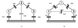
- FIGS. 3A and 3B are equivalent circuit diagrams for the even mode and the odd mode of the coupled wiring according to the first embodiment, respectively. It is a graph which shows the relationship between the width Wf of an intermediate
- 6 is a cross-sectional view of a circuit device according to a second embodiment along a signal transmission direction.
- FIG. 1 is a cross-sectional view taken along line A-A ′ of FIG. 1 and shows a cross section along the signal transmission direction of the coupled wiring according to the first embodiment.
- FIGS. 3A and 3B are equivalent circuit diagrams for the even mode and the odd mode of the coupled wiring according to the first embodiment,
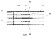
- FIG. 10 is a perspective view showing an arrangement of resonators in a circuit device according to Embodiment 3.
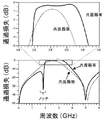
- FIG. 7 is a cross-sectional view taken along line B-B ′ in FIG. 6. It is an enlarged view of the resonator shown in FIG. It is a graph which shows a passage loss when the circuit device concerning Embodiments 2 and 3 is used as a transmission line.
- FIG. 1 is a cross-sectional view orthogonal to the signal transmission direction of the coupled wiring 10 according to the first embodiment.
- FIG. 2 is a cross-sectional view taken along line AA ′ in FIG. 1, and shows a cross section along the signal transmission direction of the coupled wiring according to the first embodiment.
- the coupling wiring 10 includes a first ground conductor 20, a second ground conductor 22, a dielectric layer 30, a first signal line conductor 40, a second signal line conductor 42, and an intermediate conductor 50.
- the first ground conductor 20 and the second ground conductor 22 are strip-shaped conductors provided so as to face each other, and are both grounded.
- the dielectric layer 30 is provided between the first ground conductor 20 and the second ground conductor 22 and is formed of, for example, an epoxy resin.
- the first signal line conductor 40 and the second signal line conductor 42 are connected to the dielectric layer 30 between the first ground conductor 20 and the second ground conductor 22.
- the conductor 22 is buried in parallel.
- the first signal line conductor 40 and the second signal line conductor 42 are strip-shaped conductors provided to face each other, and are electromagnetically coupled to each other. In the present embodiment, the case where the width of the first signal line conductor 40 and the width of the second signal line conductor 42 are the same is shown.
- the intermediate conductor 50 is a strip-shaped conductor embedded in the dielectric layer 30 between the first signal line conductor 40 and the second signal line conductor 42, and the potential thereof is a floating potential.
- the width Wf of the intermediate conductor 50 is such that the first signal line conductor 40 and the second signal line conductor 42 are the same. It is shorter than the overlapping length. More preferably, the width Wf of the intermediate conductor 50 is defined as Wc in which the first signal line conductor 40 and the second signal line conductor 42 overlap each other, and the intermediate conductor 50, the first signal line conductor 40, and the first signal line conductor 40 When the thickness of the second signal line conductor 42 is t, it is preferable to satisfy the relationship 0 ⁇ Wf ⁇ Wc ⁇ t.
- FIGS. 3A and 3B show equivalent circuit diagrams of the even mode and the odd mode when the intermediate conductor 50 is used.
- the circled numbers 1, 2, and 3 correspond to the first signal line conductor 40, the intermediate conductor 50, and the second signal line conductor 42, respectively.
- the capacitance C11 between the first signal line conductor 40 and the ground potential is smaller than the capacitance C33 between the second signal line conductor 42 and the ground potential.
- the capacity C22 is negligible.
- the impedance is fixed by C11 + C33. Therefore, in the even mode, the impedance is determined without depending on the width Wf of the intermediate conductor 50.
- the capacitance between the first signal line conductor 40 and the intermediate conductor 50 in addition to the capacitance C13 between the first signal line conductor 40 and the second signal line conductor 42 is adjusted by the capacitance C23 between C12 and the intermediate conductor 50 and the second signal line conductor 42.
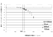
- FIG. 4 is a graph showing the relationship between the width Wf of the intermediate conductor and the even-mode impedance change rate.
- the horizontal axis of FIG. 4 indicates the width of the intermediate conductor, and the vertical axis of FIG. 4 indicates the rate of change of the even-mode impedance in the coupled wiring at the width of each intermediate conductor when there is no intermediate conductor.
- the dimensions of the coupled wiring used in the analysis are as follows.
- Width Wc of first signal line conductor 40 and second signal line conductor 42 200 ⁇ m
- the width Wf of the intermediate conductor 50 is set to the length Wc (in other words, the first signal line conductor 40 and the second signal line conductor 42) on which the first signal line conductor 40 and the second signal line conductor 42 overlap.
- the width of the first signal line conductor 40 and the second signal line conductor 42 are set to be smaller than the thickness t of the first signal line conductor 40 and the impedance change rate of the even mode is less than 1%. Almost no influence on the performance as a coupling wiring.
- circuit device A circuit device using the coupling wiring according to the first embodiment will be described.
- FIG. 5 is a cross-sectional view showing a circuit device 100 according to the second embodiment.
- the circuit device 100 according to the present embodiment one end and the other end of the first signal line conductor 40 are an input end and a ground end, respectively, and one end and the other end of the second signal line conductor 42 are a ground end and This is the output end.
- the circuit device 100 according to the present embodiment has a coupling line length of the first signal line conductor 40 and the second signal line conductor 42 of ⁇ / 4, and functions as a band pass filter (BPF).
- BPF band pass filter
- FIG. 6 is a perspective view showing the arrangement of resonators in the circuit device according to the third embodiment.
- the dielectric layer is omitted for easy understanding.
- FIG. 7 is a cross-sectional view taken along line BB ′ of FIG.
- FIG. 8 is an enlarged view of the resonator shown in FIG.
- the circuit device 100 according to the third embodiment has a configuration in which the resonator 120 is arranged in the circuit device 100 according to the second embodiment.
- the resonator 120 has a line / space of 40 ⁇ m / 40 ⁇ m and a spiral structure of 0.8 mm square, and an effective inductance L at 2 GHz is 5 nH.
- eight resonators 120 are alternately connected to the sides of the intermediate conductor 50 at a predetermined interval. Specifically, the spiral end of each resonator 120 is connected to the intermediate conductor 50, and the connection part 121 at the center of the spiral of each resonator 120 is connected to the first ground conductor 20 and the second ground conductor 22. (Not shown). From the viewpoint of suppressing unnecessary coupling, it is preferable to use a high-impedance line at the connection between the intermediate conductor 50 and the resonator 120.
- FIG. 9 is a graph showing a passage loss when the circuit device 100 according to the second and third embodiments is used as a transmission line. As shown in FIG. 9, it can be seen that by arranging the resonator 120, a steep notch is generated at 1.8 GHz, and the passband becomes flatter and wider.
- the present invention can be used for a coupling wiring having a coupling line used for transmission of a high-frequency signal and a circuit device including the coupling wiring.
Landscapes
- Control Of Motors That Do Not Use Commutators (AREA)
Abstract
Selon l'invention, un premier conducteur de masse (20) et un second conducteur de masse (22) sont des conducteurs de masse en forme de ceinture qui sont opposés l'un à l'autre. Une couche diélectrique (30) est disposée entre le premier conducteur de masse (20) et le second conducteur de masse (22) et elle est faite, par exemple, d'une résine époxy. Un premier conducteur de ligne de signal (40) et un second conducteur de ligne de signal (42) sont noyés dans la couche diélectrique (30) et sont des conducteurs en forme de ruban qui sont opposés l'un à l'autre et qui sont connectés électromagnétiquement entre eux. Un conducteur intermédiaire (50) est un conducteur en forme de ruban noyé dans la couche diélectrique (30) et disposé entre le premier conducteur de ligne de signal (40) et le second conducteur de ligne de signal (42) et le potentiel du conducteur intermédiaire (50) est un potentiel flottant. Dans une section transversale réalisée en coupant le premier conducteur de ligne de signal (40) et le second conducteur de ligne de signal (42) perpendiculairement à la direction de transmission du signal, une largeur (Wf) du conducteur intermédiaire (50) est inférieure à la longueur de superposition du premier conducteur de ligne de signal (40) et du second conducteur de ligne de signal (42).
Applications Claiming Priority (2)
| Application Number | Priority Date | Filing Date | Title |
|---|---|---|---|
| JP2010172303A JP2013214790A (ja) | 2010-07-30 | 2010-07-30 | 結合配線および回路装置 |
| JP2010-172303 | 2010-07-30 |
Publications (1)
| Publication Number | Publication Date |
|---|---|
| WO2012014493A1 true WO2012014493A1 (fr) | 2012-02-02 |
Family
ID=45529719
Family Applications (1)
| Application Number | Title | Priority Date | Filing Date |
|---|---|---|---|
| PCT/JP2011/004316 Ceased WO2012014493A1 (fr) | 2010-07-30 | 2011-07-29 | Dispositif combiné de distribution et de circuits |
Country Status (2)
| Country | Link |
|---|---|
| JP (1) | JP2013214790A (fr) |
| WO (1) | WO2012014493A1 (fr) |
Citations (4)
| Publication number | Priority date | Publication date | Assignee | Title |
|---|---|---|---|---|
| US3221274A (en) * | 1961-07-26 | 1965-11-30 | Marconi Co Ltd | Unbalanced line directional couplers and television frequency translating systems utilizing said couplers |
| JPH02106701U (fr) * | 1989-02-10 | 1990-08-24 | ||
| JPH09219607A (ja) * | 1996-02-13 | 1997-08-19 | Murata Mfg Co Ltd | 伝送線路 |
| JP2008109331A (ja) * | 2006-10-25 | 2008-05-08 | Nec Corp | 伝送線路及びこれを有する配線基板並びに半導体装置 |
-
2010
- 2010-07-30 JP JP2010172303A patent/JP2013214790A/ja active Pending
-
2011
- 2011-07-29 WO PCT/JP2011/004316 patent/WO2012014493A1/fr not_active Ceased
Patent Citations (4)
| Publication number | Priority date | Publication date | Assignee | Title |
|---|---|---|---|---|
| US3221274A (en) * | 1961-07-26 | 1965-11-30 | Marconi Co Ltd | Unbalanced line directional couplers and television frequency translating systems utilizing said couplers |
| JPH02106701U (fr) * | 1989-02-10 | 1990-08-24 | ||
| JPH09219607A (ja) * | 1996-02-13 | 1997-08-19 | Murata Mfg Co Ltd | 伝送線路 |
| JP2008109331A (ja) * | 2006-10-25 | 2008-05-08 | Nec Corp | 伝送線路及びこれを有する配線基板並びに半導体装置 |
Also Published As
| Publication number | Publication date |
|---|---|
| JP2013214790A (ja) | 2013-10-17 |
Similar Documents
| Publication | Publication Date | Title |
|---|---|---|
| US8258897B2 (en) | Ground structures in resonators for planar and folded distributed electromagnetic wave filters | |
| TWI556502B (zh) | 用於射頻積體電路的多模濾波器 | |
| US20120319797A1 (en) | Directional coupler | |
| US20100141356A1 (en) | Coupled line filter and arraying method thereof | |
| JP4740257B2 (ja) | バンドパスフィルタ | |
| JP4195036B2 (ja) | 積層型共振器 | |
| JP4598024B2 (ja) | 帯域阻止フィルタ | |
| JP2005260570A (ja) | マイクロストリップ線路導波管変換器 | |
| JP6091284B2 (ja) | 方向性結合器 | |
| US10418680B1 (en) | Multilayer coupler having mode-compensating bend | |
| JP2005117433A (ja) | フィルタ | |
| US7764147B2 (en) | Coplanar resonator and filter using the same | |
| US7525401B2 (en) | Stacked filter | |
| JP5094524B2 (ja) | 高周波結合線路および高周波フィルタ | |
| JP4600456B2 (ja) | フィルタ | |
| WO2012014493A1 (fr) | Dispositif combiné de distribution et de circuits | |
| US10418681B1 (en) | Multilayer loop coupler having transition region with local ground | |
| JP4913217B2 (ja) | ローパスフィルタ | |
| US6535078B1 (en) | Dielectric filter, dielectric duplexer, and communication system | |
| WO2011046404A2 (fr) | Dispositif de blocage cc au moyen d'une adaptation d'impédances | |
| JP4873642B2 (ja) | 導波管バンドパスフィルタ | |
| JP4762930B2 (ja) | 左手系線路 | |
| JP4757809B2 (ja) | 低域通過フィルタ | |
| JP2004104588A (ja) | バンドパスフィルタ | |
| JP5257303B2 (ja) | 方向性結合器 |
Legal Events
| Date | Code | Title | Description |
|---|---|---|---|
| 121 | Ep: the epo has been informed by wipo that ep was designated in this application |
Ref document number: 11812090 Country of ref document: EP Kind code of ref document: A1 |
|
| NENP | Non-entry into the national phase |
Ref country code: DE |
|
| 122 | Ep: pct application non-entry in european phase |
Ref document number: 11812090 Country of ref document: EP Kind code of ref document: A1 |
|
| NENP | Non-entry into the national phase |
Ref country code: JP |