WO2012046603A1 - Élément récepteur de lumière, dispositif capteur optique et procédé de fabrication d'élément récepteur de lumière - Google Patents
Élément récepteur de lumière, dispositif capteur optique et procédé de fabrication d'élément récepteur de lumière Download PDFInfo
- Publication number
- WO2012046603A1 WO2012046603A1 PCT/JP2011/072251 JP2011072251W WO2012046603A1 WO 2012046603 A1 WO2012046603 A1 WO 2012046603A1 JP 2011072251 W JP2011072251 W JP 2011072251W WO 2012046603 A1 WO2012046603 A1 WO 2012046603A1
- Authority
- WO
- WIPO (PCT)
- Prior art keywords
- layer
- light receiving
- mqw
- receiving element
- light
- Prior art date
- Legal status (The legal status is an assumption and is not a legal conclusion. Google has not performed a legal analysis and makes no representation as to the accuracy of the status listed.)
- Ceased
Links
Images




Classifications
-
- H—ELECTRICITY
- H10—SEMICONDUCTOR DEVICES; ELECTRIC SOLID-STATE DEVICES NOT OTHERWISE PROVIDED FOR
- H10F—INORGANIC SEMICONDUCTOR DEVICES SENSITIVE TO INFRARED RADIATION, LIGHT, ELECTROMAGNETIC RADIATION OF SHORTER WAVELENGTH OR CORPUSCULAR RADIATION
- H10F77/00—Constructional details of devices covered by this subclass
- H10F77/10—Semiconductor bodies
- H10F77/14—Shape of semiconductor bodies; Shapes, relative sizes or dispositions of semiconductor regions within semiconductor bodies
- H10F77/146—Superlattices; Multiple quantum well structures
-
- H—ELECTRICITY
- H10—SEMICONDUCTOR DEVICES; ELECTRIC SOLID-STATE DEVICES NOT OTHERWISE PROVIDED FOR
- H10F—INORGANIC SEMICONDUCTOR DEVICES SENSITIVE TO INFRARED RADIATION, LIGHT, ELECTROMAGNETIC RADIATION OF SHORTER WAVELENGTH OR CORPUSCULAR RADIATION
- H10F30/00—Individual radiation-sensitive semiconductor devices in which radiation controls the flow of current through the devices, e.g. photodetectors
- H10F30/20—Individual radiation-sensitive semiconductor devices in which radiation controls the flow of current through the devices, e.g. photodetectors the devices having potential barriers, e.g. phototransistors
-
- B—PERFORMING OPERATIONS; TRANSPORTING
- B82—NANOTECHNOLOGY
- B82Y—SPECIFIC USES OR APPLICATIONS OF NANOSTRUCTURES; MEASUREMENT OR ANALYSIS OF NANOSTRUCTURES; MANUFACTURE OR TREATMENT OF NANOSTRUCTURES
- B82Y20/00—Nanooptics, e.g. quantum optics or photonic crystals
-
- H—ELECTRICITY
- H10—SEMICONDUCTOR DEVICES; ELECTRIC SOLID-STATE DEVICES NOT OTHERWISE PROVIDED FOR
- H10F—INORGANIC SEMICONDUCTOR DEVICES SENSITIVE TO INFRARED RADIATION, LIGHT, ELECTROMAGNETIC RADIATION OF SHORTER WAVELENGTH OR CORPUSCULAR RADIATION
- H10F30/00—Individual radiation-sensitive semiconductor devices in which radiation controls the flow of current through the devices, e.g. photodetectors
- H10F30/20—Individual radiation-sensitive semiconductor devices in which radiation controls the flow of current through the devices, e.g. photodetectors the devices having potential barriers, e.g. phototransistors
- H10F30/21—Individual radiation-sensitive semiconductor devices in which radiation controls the flow of current through the devices, e.g. photodetectors the devices having potential barriers, e.g. phototransistors the devices being sensitive to infrared, visible or ultraviolet radiation
- H10F30/22—Individual radiation-sensitive semiconductor devices in which radiation controls the flow of current through the devices, e.g. photodetectors the devices having potential barriers, e.g. phototransistors the devices being sensitive to infrared, visible or ultraviolet radiation the devices having only one potential barrier, e.g. photodiodes
- H10F30/223—Individual radiation-sensitive semiconductor devices in which radiation controls the flow of current through the devices, e.g. photodetectors the devices having potential barriers, e.g. phototransistors the devices being sensitive to infrared, visible or ultraviolet radiation the devices having only one potential barrier, e.g. photodiodes the potential barrier being a PIN barrier
-
- H—ELECTRICITY
- H10—SEMICONDUCTOR DEVICES; ELECTRIC SOLID-STATE DEVICES NOT OTHERWISE PROVIDED FOR
- H10F—INORGANIC SEMICONDUCTOR DEVICES SENSITIVE TO INFRARED RADIATION, LIGHT, ELECTROMAGNETIC RADIATION OF SHORTER WAVELENGTH OR CORPUSCULAR RADIATION
- H10F39/00—Integrated devices, or assemblies of multiple devices, comprising at least one element covered by group H10F30/00, e.g. radiation detectors comprising photodiode arrays
- H10F39/10—Integrated devices
- H10F39/12—Image sensors
- H10F39/199—Back-illuminated image sensors
-
- H—ELECTRICITY
- H10—SEMICONDUCTOR DEVICES; ELECTRIC SOLID-STATE DEVICES NOT OTHERWISE PROVIDED FOR
- H10F—INORGANIC SEMICONDUCTOR DEVICES SENSITIVE TO INFRARED RADIATION, LIGHT, ELECTROMAGNETIC RADIATION OF SHORTER WAVELENGTH OR CORPUSCULAR RADIATION
- H10F71/00—Manufacture or treatment of devices covered by this subclass
- H10F71/127—The active layers comprising only Group III-V materials, e.g. GaAs or InP
- H10F71/1272—The active layers comprising only Group III-V materials, e.g. GaAs or InP comprising at least three elements, e.g. GaAlAs or InGaAsP
-
- H—ELECTRICITY
- H10—SEMICONDUCTOR DEVICES; ELECTRIC SOLID-STATE DEVICES NOT OTHERWISE PROVIDED FOR
- H10F—INORGANIC SEMICONDUCTOR DEVICES SENSITIVE TO INFRARED RADIATION, LIGHT, ELECTROMAGNETIC RADIATION OF SHORTER WAVELENGTH OR CORPUSCULAR RADIATION
- H10F71/00—Manufacture or treatment of devices covered by this subclass
- H10F71/127—The active layers comprising only Group III-V materials, e.g. GaAs or InP
- H10F71/1276—The active layers comprising only Group III-V materials, e.g. GaAs or InP comprising growth substrates not made of Group III-V materials
-
- H—ELECTRICITY
- H10—SEMICONDUCTOR DEVICES; ELECTRIC SOLID-STATE DEVICES NOT OTHERWISE PROVIDED FOR
- H10D—INORGANIC ELECTRIC SEMICONDUCTOR DEVICES
- H10D62/00—Semiconductor bodies, or regions thereof, of devices having potential barriers
- H10D62/80—Semiconductor bodies, or regions thereof, of devices having potential barriers characterised by the materials
- H10D62/81—Semiconductor bodies, or regions thereof, of devices having potential barriers characterised by the materials of structures exhibiting quantum-confinement effects, e.g. single quantum wells; of structures having periodic or quasi-periodic potential variation
- H10D62/815—Semiconductor bodies, or regions thereof, of devices having potential barriers characterised by the materials of structures exhibiting quantum-confinement effects, e.g. single quantum wells; of structures having periodic or quasi-periodic potential variation of structures having periodic or quasi-periodic potential variation, e.g. superlattices or multiple quantum wells [MQW]
-
- H—ELECTRICITY
- H10—SEMICONDUCTOR DEVICES; ELECTRIC SOLID-STATE DEVICES NOT OTHERWISE PROVIDED FOR
- H10F—INORGANIC SEMICONDUCTOR DEVICES SENSITIVE TO INFRARED RADIATION, LIGHT, ELECTROMAGNETIC RADIATION OF SHORTER WAVELENGTH OR CORPUSCULAR RADIATION
- H10F39/00—Integrated devices, or assemblies of multiple devices, comprising at least one element covered by group H10F30/00, e.g. radiation detectors comprising photodiode arrays
- H10F39/10—Integrated devices
- H10F39/12—Image sensors
- H10F39/18—Complementary metal-oxide-semiconductor [CMOS] image sensors; Photodiode array image sensors
- H10F39/182—Colour image sensors
- H10F39/1825—Multicolour image sensors having stacked structure, e.g. NPN, NPNPN or multiple quantum well [MQW] structures
-
- H—ELECTRICITY
- H10—SEMICONDUCTOR DEVICES; ELECTRIC SOLID-STATE DEVICES NOT OTHERWISE PROVIDED FOR
- H10F—INORGANIC SEMICONDUCTOR DEVICES SENSITIVE TO INFRARED RADIATION, LIGHT, ELECTROMAGNETIC RADIATION OF SHORTER WAVELENGTH OR CORPUSCULAR RADIATION
- H10F39/00—Integrated devices, or assemblies of multiple devices, comprising at least one element covered by group H10F30/00, e.g. radiation detectors comprising photodiode arrays
- H10F39/10—Integrated devices
- H10F39/12—Image sensors
- H10F39/18—Complementary metal-oxide-semiconductor [CMOS] image sensors; Photodiode array image sensors
- H10F39/184—Infrared image sensors
- H10F39/1847—Multispectral infrared image sensors having a stacked structure, e.g. NPN, NPNPN or multiple quantum well [MQW] structures
-
- H—ELECTRICITY
- H10—SEMICONDUCTOR DEVICES; ELECTRIC SOLID-STATE DEVICES NOT OTHERWISE PROVIDED FOR
- H10F—INORGANIC SEMICONDUCTOR DEVICES SENSITIVE TO INFRARED RADIATION, LIGHT, ELECTROMAGNETIC RADIATION OF SHORTER WAVELENGTH OR CORPUSCULAR RADIATION
- H10F39/00—Integrated devices, or assemblies of multiple devices, comprising at least one element covered by group H10F30/00, e.g. radiation detectors comprising photodiode arrays
- H10F39/80—Constructional details of image sensors
- H10F39/809—Constructional details of image sensors of hybrid image sensors
-
- H—ELECTRICITY
- H10—SEMICONDUCTOR DEVICES; ELECTRIC SOLID-STATE DEVICES NOT OTHERWISE PROVIDED FOR
- H10F—INORGANIC SEMICONDUCTOR DEVICES SENSITIVE TO INFRARED RADIATION, LIGHT, ELECTROMAGNETIC RADIATION OF SHORTER WAVELENGTH OR CORPUSCULAR RADIATION
- H10F39/00—Integrated devices, or assemblies of multiple devices, comprising at least one element covered by group H10F30/00, e.g. radiation detectors comprising photodiode arrays
- H10F39/80—Constructional details of image sensors
- H10F39/811—Interconnections
-
- Y—GENERAL TAGGING OF NEW TECHNOLOGICAL DEVELOPMENTS; GENERAL TAGGING OF CROSS-SECTIONAL TECHNOLOGIES SPANNING OVER SEVERAL SECTIONS OF THE IPC; TECHNICAL SUBJECTS COVERED BY FORMER USPC CROSS-REFERENCE ART COLLECTIONS [XRACs] AND DIGESTS
- Y02—TECHNOLOGIES OR APPLICATIONS FOR MITIGATION OR ADAPTATION AGAINST CLIMATE CHANGE
- Y02E—REDUCTION OF GREENHOUSE GAS [GHG] EMISSIONS, RELATED TO ENERGY GENERATION, TRANSMISSION OR DISTRIBUTION
- Y02E10/00—Energy generation through renewable energy sources
- Y02E10/50—Photovoltaic [PV] energy
- Y02E10/544—Solar cells from Group III-V materials
-
- Y—GENERAL TAGGING OF NEW TECHNOLOGICAL DEVELOPMENTS; GENERAL TAGGING OF CROSS-SECTIONAL TECHNOLOGIES SPANNING OVER SEVERAL SECTIONS OF THE IPC; TECHNICAL SUBJECTS COVERED BY FORMER USPC CROSS-REFERENCE ART COLLECTIONS [XRACs] AND DIGESTS
- Y02—TECHNOLOGIES OR APPLICATIONS FOR MITIGATION OR ADAPTATION AGAINST CLIMATE CHANGE
- Y02P—CLIMATE CHANGE MITIGATION TECHNOLOGIES IN THE PRODUCTION OR PROCESSING OF GOODS
- Y02P70/00—Climate change mitigation technologies in the production process for final industrial or consumer products
- Y02P70/50—Manufacturing or production processes characterised by the final manufactured product
Definitions
- the present invention relates to a III-V compound semiconductor light receiving element, an optical sensor device, and a method for manufacturing the light receiving element. More specifically, a light receiving element, an optical sensor device, and a type 2 multiple quantum well structure (MQW: Multiple-Quantum Well) having a light receiving sensitivity in the near-infrared long wavelength region are included in the light receiving layer.
- the present invention relates to a method for manufacturing a light receiving element.
- Non-Patent Document 1 discloses a photodiode having a light-receiving layer of InGaAs / GaAsSb type 2 MQW lattice-matched to an InP substrate of a III-V compound semiconductor.
- This MQW is composed of a repetition number of 150 (a number of pairs of 150) with InGaAs having a thickness of 5 nm and GaAsSb having a thickness of 5 nm as a pair.
- a cutoff wavelength of about 2.39 ⁇ m can be obtained.
- the light receiving element has a structure in which the cap layer on the opposite side to the InP substrate is a p-conductivity type with respect to the light-receiving layer, the InP substrate is an n-conductivity type, and light is incident from the back side of the InP substrate.
- Non-Patent Document 2 discloses the wavelength dependence of sensitivity for a photodiode having the same structure as described above. The sensitivity is not flat with respect to the wavelength but shows a strong wavelength dependence.
- the sensitivity of the photodiode having the MQW of type 2 InGaAs (thickness 5 nm) / GaAsSb (thickness 5 nm) is relatively high on the long wavelength side near the wavelength of 2.3 ⁇ m, but greatly decreases near the wavelength of 1.5 ⁇ m. This drop in sensitivity near the wavelength of 1.5 ⁇ m is not preferable in spectral analysis or the like.
- the sensitivity is preferably flat over the entire wavelength range. However, it is not preferable that the sensitivity is low stability, and it is preferable that the sensitivity be flat or fluctuate with respect to the wavelength while being above a predetermined level.
- the present invention relates to a light receiving element having an MQW of type 2 and capable of preventing a drop in sensitivity in a short wavelength range while improving the sensitivity over the entire wavelength range where light can be received. It is an object of the present invention to provide an optical sensor device and a method for manufacturing a light receiving element.
- the light receiving element may be an element having a single pixel, or may be an element arranged in a one-dimensional or two-dimensional array.
- the light-receiving element of the present invention is formed on a group III-V compound semiconductor substrate and has pixels.
- the light receiving element includes a type 2 MQW light receiving layer located on a substrate, and MQW includes two or more pairs of two different III-V compound semiconductor layers, and two different III- Among the group V compound semiconductor layers, the layer having the higher valence band potential is made thinner than the other layer.
- the electrons in the valence band are excited to the conduction band, and vacancies are generated in the valence band. That is, an electron / hole pair is formed by light reception.
- the electrons reach the n-side electrode and the vacancies reach the p-side electrode and need to be detected as charges or currents.
- One of the n-side electrode and the p-side electrode needs to be arranged for each pixel. Electrons move through the conduction band and reach the n-side electrode, and holes move through the valence band and reach the p-side electrode, whereby the charge or current is detected.
- the effective mass in the conduction band of electrons in a compound semiconductor is about 0.05 m (m: mass of free electrons), whereas the effective mass of holes in the valence band (heavy holes) Is large, for example, about 10 times or more of electrons.
- the phenomenon peculiar to the reception of the type 2 MQW is as follows. That is, in light reception on the long wavelength side in Type 2 MQW, holes are generated in a layer having a higher valence band (hereinafter referred to as a higher layer).
- the valence band of the adjacent layer (the layer with the lower valence band (hereinafter referred to as the lower layer)) forms a well-type barrier with respect to the valence band of the higher layer. For this reason, the holes generated by light reception have resistance to movement by the potential barrier formed by the adjacent lower layer in addition to the extremely large effective mass compared to the electrons as described above.
- In Type 2 MQW light reception on the long wavelength side occurs at the interface between the higher layer and the lower layer.
- Type 2 MQW is used to expand the light receiving sensitivity to the longer wavelength side.
- the sensitivity in the long wavelength region cannot be increased beyond the practical level.
- the number of pairs is 50 or more.
- the following two arrangement configurations (F1) and (F2) cover all arrangement configurations, but are classified for the purpose of organizing the concept.
- the present invention has a beneficial effect.
- (F1) When the incident surface and the p-side electrode are in a positional relationship such that the MQW is sandwiched between them, the light on the short wavelength side tends to be received at the MQW end near the incident surface. For this reason, of the generated holes / electrons, the holes cannot reach the p-side electrode unless they move through almost the entire thickness of the MQW. Holes are more likely to disappear during the movement of MQW, resulting in a decrease in sensitivity.
- the wavelength limit refers to a longer wavelength limit.
- the wavelength limit at which light can be received in type 2 MQW is determined by the difference between the ground state energy of the valence band of the higher layer and the ground state energy of the conduction band of the lower layer. Generally, when the thickness of the quantum well layer is reduced, the energy of the ground state for electrons increases greatly, but the increase of the energy of the ground state for holes is small. The reason is that the effective mass greatly affects the energy level of electrons or holes.
- the energy level is low and the ground state energy level is also low.
- Light reception is possible by reducing the thickness of the higher layer (holes are generated in its valence band) and the lower layer (electrons are generated in its conduction band) to a specified level or more.
- the critical wavelength limit hardly changes.
- high sensitivity can be maintained by setting MQW of 50 pairs or more. (E2) In a light reception standby state, a reverse bias voltage is applied between both electrodes to apply an electric field in the MQW. Holes and electrons move through the MQW driven by this electric field.
- the strength of the electric field generated in the MQW by a constant bias voltage can be increased.
- the disappearance of holes can be suppressed and the sensitivity can be increased.
- E3 The effect of suppressing the disappearance of holes is effective regardless of the wavelength of the received light.
- the film thickness of the layer having the higher valence band potential can be made 1 nm or more thinner than the film thickness of the other layer.
- the total thickness of the MQW can be reliably reduced while securing a predetermined number or more of pairs.
- the sensitivity can be increased in the entire wavelength region below the wavelength limit.
- (F1) it is possible to improve the sensitivity of light in a short wavelength range in which light reception is likely to occur at an end far from the p-side electrode.
- a cap layer located on the light receiving layer is provided, and the pixel region in the cap layer is of p conductivity type, and the back surface of the substrate can be a light incident surface.
- the p-side electrode is located on a p-conductivity type pixel. Holes generated by light reception tend to disappear while moving in the valence band toward the p-side electrode. As a result, sensitivity decreases. In particular, when light is received at the end of the MQW close to the substrate, the holes generated there do not contribute to sensitivity unless they move through almost the entire thickness of the MQW. As described above, in the present invention, the total thickness of MQW can be reduced without significantly affecting the wavelength limit of light reception.
- a cap layer located on the light receiving layer is provided, and the pixel region in the cap layer is of n conductivity type, and light can enter from the cap layer side.
- the p-side electrode is a ground electrode. Since the incident light is usually received as soon as it is incident, holes cannot contribute to sensitivity unless they move almost the total thickness of the MQW and reach the p-side electrode. In particular, light on the short wavelength side tends to be received immediately after entering the MQW, and therefore tends to not contribute to sensitivity. However, in the present invention, since the total thickness of the MQW is reduced without significantly affecting the wavelength limit of light reception and maintaining the sensitivity on the long wavelength side, the frequency of annihilation during the movement of the holes during MQW movement is reduced. , And sensitivity can be maintained. In particular, it is effective for preventing a decrease in sensitivity on the short wavelength side.
- the substrate can be an InP substrate.
- InP substrate As a result, it is possible to obtain a light receiving element having a sensitivity in the near infrared region and having a low dark current due to good crystallinity using an InP substrate that has been used for many years.
- the layer having the higher valence band potential can contain Ga, As, and Sb. This makes it possible to form a III-V group compound semiconductor layer such as GaAsSb, GaAsSbN, or GaAsSbP having a high valence band potential.
- a III-V group compound semiconductor layer such as GaAsSb, GaAsSbN, or GaAsSbP having a high valence band potential.
- an InP substrate since the lattice matching is good, a high-quality light receiving element with low dark current can be obtained.
- MQW is a type 2 MQW composed of a pair of In x Ga 1-x As (0.38 ⁇ x ⁇ 0.68) and GaAs y Sb 1-y (0.36 ⁇ y ⁇ 0.62) can do.
- a high-quality light-receiving element that can cover the wavelength limit of light reception that is 2.5 ⁇ m or more and close to 3 ⁇ m.
- the light receiving element can have a sensitivity to light having a wavelength of 1500 nm of 0.5 A / W or more. As a result, since the sensitivity on the short wavelength side is too small, information processing such as spectrum analysis is not hindered.
- a regrowth interface between the top surface of the MQW and the bottom surface of the cap layer. Since impurities such as oxygen and carbon are concentrated on the regrowth interface, the crystallinity of the epitaxial layer formed on the regrowth interface is deteriorated, resulting in an increase in dark current and the like. By not having a regrowth interface in the above portion, a good crystal layer can be obtained and dark current can be reduced.
- the optical sensor device of the present invention is characterized by using any of the light receiving elements described above.
- high-quality light-receiving elements that have sensitivity in the near-infrared region and low dark current can be used at room temperature in fields that have previously been impossible to sense without cooling devices, such as living organisms and the environment. And a small device can be provided. If a cooling device is required, power for that purpose or supply of liquid nitrogen or the like is required. For this reason, large restrictions are imposed in terms of size, cooling maintenance, and cost for cooling maintenance.
- the present invention enables highly accurate sensing for a field that has been impossible for such a reason.
- the method for manufacturing a light receiving element of the present invention manufactures a light receiving element formed on a substrate of a III-V compound semiconductor and having pixels.
- the manufacturing method includes a step of growing a type 2 MQW light-receiving layer on a substrate.
- the first layer and the second layer of a group III-V compound semiconductor are paired.
- the potential of the valence band of the first layer is higher than the potential of the valence band of the second layer, and in the MQW growth process, the thickness of the first layer is made thinner than the thickness of the second layer. , 50 or more pairs are stacked.
- the method further includes a step of forming a layer including a group III-V compound semiconductor.
- the step of forming MQW and the step of forming a layer including a group III-V compound semiconductor From the start of the growth of MQW to the end of the growth of the layer containing the III-V compound semiconductor, the same growth tank is formed by the all-organic vapor phase growth method (the all-organic MOVPE method) so as not to include the step of forming the growth interface. Can grow within. Thereby, a laminate having excellent crystallinity can be formed on the MQW.
- the semiconductor element or the like of the present invention it is possible to prevent a drop in sensitivity in a short wavelength range while improving sensitivity over the entire wavelength range where light can be received using type 2 MQW.
- FIG. 1 is an optical sensor device including a light receiving element of the present invention in which a plurality of pixels are arranged. It is a figure which shows the measurement result of PL peak wavelength (median value) of each test body in Example 1. It is a figure which shows the influence (measurement result) of the total film thickness of MQW and the wavelength which acts on the sensitivity R of each test body in Example 2.
- FIG. 1 shows the measurement result of PL peak wavelength (median value) of each test body in Example 1.
- FIG. 1 shows the influence (measurement result) of the total film thickness of MQW and the wavelength which acts on the sensitivity R of each test body in Example 2.
- InP substrate 2 buffer layer (InP and / or InGaAs), 3 type 2 MQW light-receiving layer, 3a layer with higher valence band potential (GaAsSb), 3b layer with lower valence band potential (InGaAs) 3u 1 pair, 4 InGaAs layer (diffusion concentration distribution adjustment layer), 5 InP cap layer, 6 p-type region, 10 optical sensor device (detection device), 11 p-side electrode (pixel electrode), 12 ground electrode (n-side) Electrode), 12b bump, 15 pn junction, 16 interface between MQW and InGaAs layer, 17 interface between InGaAs layer (diffusion concentration distribution adjusting layer) and InP window layer, 35 AR (antireflection) film, 36 selective diffusion mask pattern 39 Bond bump, 43 Protective film (Si N film), 50 light receiving element (light receiving element array), 50a wafer (intermediate product), 60, all organic MOVPE film forming device, 61, infrared temperature monitoring
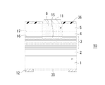
- FIG. 1A is a diagram showing a light receiving element 50 according to an embodiment of the present invention.
- the light receiving element 50 has an InP semiconductor stacked structure (epitaxial wafer) of the following configuration on the InP substrate 1.
- InP semiconductor stacked structure epipitaxial wafer
- FIG. 1A light is incident from the back side of the InP substrate 1.
- it can also take the structure which injects from an epitaxial side.
- the p-type region 6 is positioned so as to reach the MQW light-receiving layer 3 from the surface of the InP cap layer 5.
- the p-type region 6 is formed by selective diffusion of p-type impurity Zn from the opening of the selective diffusion mask pattern 36 of the SiN film.
- Zn is diffused and introduced into the inner periphery of the peripheral portion of the light receiving element 50 in a plan view.
- a p-side electrode 11 made of AuZn is provided in the p-type region 6, and an n-side electrode 12 made of AuGeNi is provided in ohmic contact with the back surface of the InP substrate 1.
- the InP substrate 1 is doped with n-type impurities and has a predetermined level of conductivity. However, the InP substrate 1 may not have conductivity.
- the n-side electrode 12 is disposed so as to be in ohmic contact with the n-type InP buffer layer 2.
- An SiON antireflection film 35 is provided on the back surface of the InP substrate 1 so that light enters from the back surface side of the InP substrate. Accordingly, the light receiving element 50 shown in FIG. 1A corresponds to the arrangement configuration (F1).
- a pn junction 15 is formed at a position corresponding to the boundary front of the p-type region 6, and a reverse bias voltage is applied between the p-side electrode 11 and the n-side electrode 12.
- a depletion layer is formed more widely on the side where the n-type impurity concentration is low (n-type impurity background).
- the n-type impurity background in the MQW light-receiving layer 3 is about 5E15 (5 ⁇ 10 15 ) cm ⁇ 3 or less in terms of n-type impurity concentration (carrier concentration).
- the position 15 of the pn junction is determined by the intersection of the background (n-type carrier concentration) of the light-receiving layer 3 of the multiple quantum well and the concentration profile of the p-type impurity Zn.
- the InGaAs diffusion concentration distribution adjusting layer 4 is arranged for adjusting the concentration distribution of the p-type impurity in the MQW constituting the light receiving layer 3.
- the InGaAs diffusion concentration distribution adjusting layer 4 may be omitted.
- the Zn concentration is preferably 5E16 (5 ⁇ 10 16 ) cm ⁇ 3 or less.
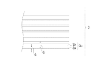
- FIG. 1B is a cross-sectional view showing the MQW constituting the light receiving layer 3.
- the light receiving layer 3 is a type 2 MQW in which InGaAs 3b and GaAsSb 3a are paired 3u.
- the number of pairs is 50 or more and 700 or less, and if the total thickness becomes excessive as will be described later, the sensitivity on the short wavelength side is lowered.
- the feature of the present invention is that, among the two compound semiconductors constituting the pair 3u, the layer having the higher valence band is made thinner than the layer having the lower valence band.
- the valence band is higher in GaAsSb3a than in InGaAs3b.
- the thickness of GaAsSb3a is made thinner than the thickness of InGaAs3b.
- InGaAs may be 5 nm / GaAsSb 2 nm.
- the light receiving element has the following purposes.
- the sensitivity should be as long as possible in the near infrared region.
- M2 High sensitivity in the entire near infrared wavelength region.
- M3 Avoid a sudden drop in sensitivity on the short wavelength side, and make the wavelength dependence moderate or preferably flat. In particular, avoid a sharp drop near the wavelength of 1.5 ⁇ m.
- FIG. 2 is a diagram for explaining the technical contents of the present invention.
- type 2 MQW light having a long wavelength, that is, a transition with a small energy difference is possible for electrons in the light receiving element.
- the electrons in the valence band of GaAsSb having the higher potential in the valence band transition to the conduction band of InGaAs, which has the lower valence band potential, so that a transition with a small energy difference or light with a long wavelength can be received.
- Holes generated in the valence band must move in the MQW 3 in order to reach the p-side electrode, and as described above, they disappear during this time and become a major factor in sensitivity reduction.
- the total thickness of MQW3 may be reduced.
- the reason is that the distance that must be moved against the well-type potential barrier is shortened. Further, an accompanying increase in electric field strength (an increase in driving force) can be expected.
- reducing the thickness of each layer uniformly to reduce the total thickness of the MQW has unacceptable side effects. For the explanation of the side effects, a little preparation is made below.
- the energy level of holes in the well-type potential in the valence band and the energy level of electrons in the well-type potential in the conduction band can be approximated by the following model. That is, the well width is finite and can be approximated by the energy level of electrons or holes in a well-type potential of infinite depth (height). According to the model, the energy level is expressed by the following equation (M).
- Ec n h 2 n c 2 / (8d 2 2 m 2 * ) (2)
- d 2 is the thickness of the lower valence band potential (eg, InGaAs).
- M 2 * effective mass of electrons
- the effective mass of holes (m 1 * ) in equation (1) is significantly different from the effective mass of electrons (m 2 * ) in equation (2), and the effective mass of holes is approximately larger than the effective mass of electrons. A point that is about 10 times larger is very important and forms the basis of the present invention.
- the description returns to the inconvenience when the MQW layers are uniformly thinned.
- the wavelength ⁇ max of the light having a limit wavelength that can be received is the difference between the ground level Ec 1 in the well-type potential of the conduction band of InGaAs and the ground level Eb 1 in the well-type potential of the valence band of GaAsSb.
- (Ec 1 ⁇ Eb 1 ) hc / ⁇ max is established.
- the energy difference (Ec 1 ⁇ Eb 1 ) becomes large, and the wavelength limit for receiving light is greatly shifted to the short wavelength side. That is, the critical wavelength that can be received unless the thickness is uniformly reduced increases the band gap or energy difference, and cannot be received. This is unacceptable for a light receiving element having the purpose of (M1) and trying to expand the light receiving sensitivity to the long wavelength side as much as possible.
- the effective mass of holes is about 10 times or more larger than the effective mass of electrons, so the hole ground level is originally about 10 times lower than that of electrons. (The difference from the vacuum state of each ground level). For this reason, when both GaAsSb and InGaAs are similarly reduced in thickness, the degree of increase in the ground level of electrons in the well-type potential of the conduction band in FIG. 2 is very large compared to holes. . In other words, it is about ten times larger than the degree of increase in the ground level of holes in the well-type potential of the valence band. When the thickness is uniformly reduced, the band gap or the energy difference is enlarged mainly by an increase in the ground level of electrons in the conduction band.
- the basic idea of the present invention is to reduce the total thickness of the MQW without significantly reducing the longest wavelength that can be received by reducing only the thickness d 1 of the higher valence band potential (GaAsSb). is there.
- the following advantages can be obtained.
- E1 Even if holes are generated far away from the p-side electrode, the total thickness Do is greatly reduced as shown in FIG. 3A, so that the holes can reach the p-side region or the p-side electrode.
- the possibility increases and the sensitivity can be improved. In particular, it light in the short wavelength side, so tends to generate immediately received by the positive holes contained in the MQW is strong, conventionally, as shown in FIG.
- both GaAsSb 103a and InGaAs 103b constituting the pair 103u have the same thickness of 5 nm as in the prior art.
- sensitivity can be ensured by reducing the total thickness of MQW according to the present invention. This not only improves the sensitivity over the wavelength range where light can be received, but also can more effectively suppress a drop in sensitivity particularly on the short wavelength side. As a result, the sensitivity with respect to the wavelength can be flattened or the fluctuation can be moderated.
- E2 When reverse bias voltage V of the same magnitude is applied, the electric field is increased by reducing the total thickness of MQW3.
- FIG. 4 shows a piping system of the all-organic MOVPE film forming apparatus 60 and the like.
- a quartz tube 65 is disposed in the reaction chamber (chamber) 63, and a raw material gas is introduced into the quartz tube 65.
- a substrate table 66 is disposed in the quartz tube 65 so as to be rotatable and airtight.
- the substrate table 66 is provided with a heater 66h for heating the substrate.
- the temperature of the surface of the wafer 50 a during film formation is monitored by the infrared temperature monitor device 61 through a window 69 provided in the ceiling of the reaction chamber 63.
- This monitored temperature is a temperature at the time of growth or a temperature called a film forming temperature or a substrate temperature.
- a temperature at the time of growth or a temperature called a film forming temperature or a substrate temperature.
- 400 ° C. or more and 560 ° C. or less are temperatures measured by this temperature monitor.
- the forced exhaust from the quartz tube 65 is performed by a vacuum pump.
- the source gas is supplied by a pipe communicating with the quartz tube 65.
- the all organic MOVPE method is characterized in that all raw material gases are supplied in the form of an organometallic gas.
- source gases such as impurities are not specified, but impurities are also introduced in the form of an organometallic gas.
- the raw material of the organometallic gas is put in a thermostat and kept at a constant temperature. Hydrogen (H 2 ) and nitrogen (N 2 ) are used as the carrier gas.
- the organometallic gas is transported by a transport gas, and is sucked by a vacuum pump and introduced into the quartz tube 65.
- the amount of the carrier gas is accurately adjusted by an MFC (Mass Flow Controller). Many flow controllers, solenoid valves, and the like are automatically controlled by a microcomputer.
- the film thickness of the MQW 3 is controlled by setting a program and controlling the flow rate controller, the electromagnetic valve, and the like.
- the n-type InP buffer layer 2 is epitaxially grown on the S-doped n-type InP substrate 1 to a film thickness of 150 nm.
- TeESi tetraethylsilane
- TMIn trimethylindium
- TBP tertiary butylphosphine
- the InP buffer layer 2 may be grown using an inorganic raw material PH 3 (phosphine). In the growth of the InP buffer layer 2, even if the growth temperature is about 600 ° C.
- the crystallinity of the InP substrate located in the lower layer is not deteriorated by heating at about 600 ° C.
- the MQW containing GaAsSb is formed in the lower layer, it is necessary to strictly maintain the substrate temperature within a range of, for example, a temperature of 400 ° C. or higher and 560 ° C. or lower. The reason is that when heated to about 600 ° C., the crystallinity of GaAsSb is greatly deteriorated due to heat damage, and when the InP cap layer is formed at a temperature lower than 400 ° C., the decomposition efficiency of the source gas is greatly increased. Therefore, the impurity concentration in the InP layer increases, and a high-quality InP cap layer cannot be obtained.
- a type 2 MQW light-receiving layer 3 having InGaAs / GaAsSb as a pair of quantum wells is formed.
- the thickness of GaAsSb3a in the quantum well is preferably about 2 nm, and the thickness of InGaAs3b is preferably 5 nm, for example.
- MQW light-receiving layer 3 is formed by stacking 250 pairs of quantum wells.
- triethylgallium (TEGa), tertiary butylarsine (TBAs), and trimethylantimony (TMSb) are used.
- TEGa, TMIn, and TBAs can be used.
- These source gases are all organometallic gases, and the molecular weight of the compound is large. Therefore, it can be completely decomposed at a relatively low temperature of 400 ° C. or higher and 560 ° C. or lower and contribute to crystal growth.
- the MQW light-receiving layer 3 can be made sharp in the composition change at the interface of the quantum well by the all-organic MOVPE method. As a result, highly accurate spectrophotometry can be performed.
- the raw material for Ga (gallium) may be TEGa (triethylgallium) or TMGa (trimethylgallium).
- the raw material for In (indium) may be TMIn (trimethylindium) or TEIn (triethylindium).
- TBAs tertiary butylarsine
- TMAs trimethylarsenic
- Sb antimony
- TMSb trimethylantimony
- TESb triethylantimony
- TIPSb triisopropylantimony
- TDMASb tridimethylaminoantimony
- a semiconductor element having a low MQW impurity concentration and excellent crystallinity can be obtained.
- a light receiving element when used in a light receiving element, a light receiving element with a small dark current and a high sensitivity can be obtained.
- an optical sensor device capable of capturing a clearer image such as an imaging device, can be obtained.
- the source gas is transported through the piping, introduced into the quartz tube 65, and exhausted. Any number of source gases can be supplied to the quartz tube 65 by increasing the number of pipes. For example, even a dozen kinds of source gases are controlled by opening and closing the electromagnetic valve.
- the flow rate of the source gas is controlled by a flow rate controller (MFC) shown in FIG. 4, and the flow into the quartz tube 65 is turned on and off by opening and closing the electromagnetic valve.
- MFC flow rate controller
- the quartz tube 65 is forcibly exhausted by a vacuum pump. There is no stagnation in the flow of the source gas, and it is performed smoothly and automatically. Therefore, the composition is switched quickly when forming the quantum well pair. As shown in FIG.
- the temperature distribution of the source gas does not have the directionality as the source gas inflow side or the outlet side. Further, since the wafer 50a revolves on the substrate table 66, the flow of the source gas near the surface of the wafer 50a is in a turbulent state, and even the source gas near the surface of the wafer 50a contacts the wafer 50a. Except for the raw material gas, it has a large velocity component in the flow direction from the introduction side to the exhaust side. Therefore, most of the heat flowing from the substrate table 66 to the source gas through the wafer 50a is always exhausted together with the exhaust gas. For this reason, a large temperature gradient or temperature step is generated in the vertical direction from the wafer 50a through the surface to the source gas space.
- the substrate temperature is heated to a low temperature range of 400 ° C. or more and 560 ° C. or less.
- a low temperature range 400 ° C. or more and 560 ° C. or less.
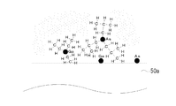
- FIG. 5A is a diagram showing the flow of organometallic molecules and the flow of temperature
- FIG. 5B is a schematic diagram of organometallic molecules on the substrate surface.
- organometallic molecules in a range in contact with the wafer surface and molecules located within the thickness range of several organometallic molecules from the wafer surface mainly contribute to crystal growth.
- the outer organometallic molecules are discharged out of the quartz tube 65 with almost no decomposition.
- the organometallic molecules located outside enter the replenishment.
- the range of the organometallic molecules that can participate in crystal growth is limited to a thin source gas layer on the surface of the wafer 50a by making the wafer surface temperature slightly higher than the temperature at which the organometallic molecules decompose. it can.
- phase separation occurs in the GaAsSb layer of the multiple quantum well structure when grown at a temperature of about 600 ° C., and the crystal growth surface of the multiple quantum well structure that is clean and excellent in flatness, and excellent A multiple quantum well structure having periodicity and crystallinity cannot be obtained.
- the growth temperature is set to a temperature range of 400 ° C. or more and 560 ° C. or less (deposition factor 2).
- This film formation method is an all-organic MOVPE method, and all the source gases are organometallic gases with high decomposition efficiency. (Film formation factor 3) strongly depends on film formation factor 1.
- an InGaAs diffusion concentration distribution adjustment layer 4 is located on the type 2 MQW light-receiving layer 3, and an InP cap layer 5 is formed on the InGaAs diffusion concentration distribution adjustment layer 4. positioned.
- the p-type region 6 is provided by selectively diffusing Zn of the p-type impurity from the opening of the selective diffusion mask pattern 36 provided on the surface of the InP cap layer 5.
- a pn junction 15 or a pi junction 15 is formed at the tip of the p-type region 6.
- a depletion layer is formed by applying a reverse bias voltage to the pn junction 15 or the pi junction 15 to capture charges due to photoelectron conversion, and to make the brightness of the pixel correspond to the amount of charges.
- the p-type region 6 or the pn junction 15 or the pi junction 15 is a main part constituting the pixel.
- the p-side electrode 11 that is in ohmic contact with the p-type region 6 is a pixel electrode, and reads the above charges for each pixel with the n-side electrode 12 that is set to the ground potential.
- the selective diffusion mask pattern 36 is left as it is on the surface of the InP cap layer around the p-type region 6. Further, a protective film such as SiON not shown is coated.
- the selective diffusion mask pattern 36 is left as it is.
- a surface level is formed at the boundary with the p-type region on the surface of the cap layer, and the dark current is formed. This is because of the increase.
- the growth continues in the same film forming chamber or quartz tube 65 by the all organic MOVPE method until the formation of the InP cap layer 5 is completed. That is, before the InP cap layer 5 is formed, the wafer 50a is not taken out from the film forming chamber, and the InP cap layer 5 is not formed by another film forming method.
- the MQW is formed as described above
- the interfaces 16 and 17 are not regrowth interfaces. For this reason, the concentrations of oxygen and carbon are both less than 1E17 (1 ⁇ 10 17 ) cm ⁇ 3 , and charge leakage does not occur particularly at the intersection line between the p-type region 6 and the interface 17.
- the InP cap layer 5 is formed, when the p-type impurity Zn is introduced from the InP cap layer 5 so as to reach the MQW light-receiving layer 3 by the selective diffusion method, the crystallinity is increased when high-concentration Zn enters the MQW.
- InGaAs diffusion concentration distribution layer 4 is provided for the adjustment.
- the InGaAs diffusion concentration distribution adjustment layer 4 may be arranged as described above, but may not be provided.
- the p-type region 6 is formed by the selective diffusion described above, and the pn junction 15 or the pi junction 15 is formed at the tip thereof. Even when the InGaAs diffusion concentration distribution adjusting layer 4 is inserted, since the InGaAs has a small band gap, the electric resistance of the light receiving element can be lowered even if it is non-doped. By reducing the electrical resistance, it is possible to improve the responsiveness and obtain a moving image with good image quality.
- the undoped InP cap layer 5 is epitaxially grown to a thickness of, for example, 0.8 ⁇ m by the all-organic MOVPE method continuously with the wafer 50a being placed in the same quartz tube 65. It is good.
- the growth temperature of the InP cap layer 5 can be made 400 ° C. or more and 560 ° C. or less, and further 535 ° C. or less.
- the MQW GaAsSb located under the InP cap layer 5 is not damaged by heat, and the MQW crystallinity is not impaired.
- the substrate temperature must be strictly maintained within a range of, for example, a temperature of 400 ° C. or higher and 560 ° C. or lower.
- the reason is that when heated to about 600 ° C., the crystallinity of GaAsSb is greatly deteriorated due to heat damage, and when the InP cap layer 5 is formed at a temperature lower than 400 ° C., the decomposition efficiency of the source gas is increased. Since it significantly decreases, the impurity concentration in the InP cap layer 5 increases, and the high quality InP cap layer 5 cannot be obtained.
- the interface between the InGaAs diffusion concentration distribution adjusting layer and the InP cap layer was a regrowth interface once exposed to the atmosphere.
- the regrowth interface by secondary ion mass spectrometry, one of oxygen concentration of 1E17 (1 ⁇ 10 17 ) cm ⁇ 3 or more and carbon concentration of 1E17 (1 ⁇ 10 17 ) cm ⁇ 3 or more is used. Can be specified by filling.
- the regrowth interface forms a crossing line with the p-type region, and a charge leak occurs at the crossing line, thereby significantly degrading the image quality.
- an InP cap layer is grown by a simple MOVPE method using phosphine (PH 3 ) as a raw material of phosphorus
- the decomposition temperature of phosphine is high, so that the occurrence of damage due to heat of GaAsSb located in the lower layer is induced and MQW is induced. It will harm the crystallinity.
- FIG. 6 is a flowchart of a manufacturing method of the light receiving element 50 of FIG. 1A.
- this manufacturing method only the organic metal gas is used as the source gas (deposition factor 3), the growth temperature is lowered (deposition factor 2), and until the formation of the InP cap layer 5 is completed. Therefore, it is important to have no recrystallization interface (deposition factor 4). As a result, it is possible to efficiently manufacture a large number of photodiodes having low charge leakage, excellent crystallinity, and having light receiving sensitivity in the near-infrared wavelength region.
- the light receiving element 50 has a single pixel. However, in the present invention, a plurality of pixels may be used and the arrangement may be one-dimensional or two-dimensional.
- FIG. 7 is a diagram showing the optical sensor device 10 including a light receiving element array (semiconductor element) 50 in which a plurality of pixels are arranged. Optical parts such as lenses are omitted. Although a protective film 43 made of a SiON film is shown in FIG. 7, it is actually arranged in FIG. 1A.
- the light receiving element array 50 has the same laminated structure as that of the light receiving elements shown in FIG. 1A, and is different in that a plurality of light receiving elements or pixels P are arranged.
- the interfaces 16 and 17 are not regrowth interfaces, and the concentration of impurities such as oxygen and carbon is as low as less than 1E17 (1 ⁇ 10 17 ) cm ⁇ 3 .
- the light receiving element array 50 is connected to a CMOS 70 constituting a readout circuit (Read-Out IC).
- the readout electrode (not shown) of the CMOS 70 and the pixel electrode (p-side electrode) 11 of the light receiving element array 50 are bonded with the bonding bump 39 interposed.
- a common ground electrode (n-side electrode) 12 for each pixel of the light receiving element array 50 and a ground electrode (not shown) of the CMOS 70 are joined via bumps 12b.
- An imaging device or the like can be obtained by combining the CMOS 70 and the light receiving element array 50 and integrating light reception information for each pixel.
- the light-receiving element array (semiconductor element) 50 of the present invention has sensitivity up to a long wavelength region and has a small dark current (leakage current), and therefore, inspection of living organisms such as animals and plants, environmental monitoring, etc. By using this, high-precision inspection can be performed.
- Example 1-Invariance of a long wavelength range in which light can be received by a light receiving element according to the present invention Using the light receiving element 50 having the same structure as that of the semiconductor element 50 shown in FIG. 1A as a basic structure, the following test body having a changed MQW structure was prepared, and verification of a long wavelength region capable of receiving light was performed. The manufacturing method followed the above-mentioned method. Evaluation of the long wavelength range which can receive light was performed by measuring PL (Photoluminescence) peak wavelength. The measurement temperature is room temperature (25 ° C.).
- the type 2 (InGaAs / GaAsSb) MQW of the present invention may or may not be a strain compensation superlattice structure.
- ⁇ is the lattice mismatch degree of the entire multi-quantum well structure
- ⁇ ⁇ ( ⁇ ) where the lattice mismatch degree of InGaAs in (GaAsSb / InGaAs) is ⁇ 1 and the lattice mismatch degree of GaAsSb is ⁇ 2.
- the strain can be changed by changing the composition of InGaAs and GaAsSb within a minute range and changing the degree of lattice mismatch.
- Each test body shown below (examples of the present invention and comparative examples) was obtained by changing the composition to change the strain ( ⁇ ), and each test body belongs to the number of strain values, Those having the same MQW thickness configuration were displayed as the same specimen.
- ⁇ Invention Sample A> (InGaAs thickness 5 nm / GaAsSb 2 nm) as one pair, 250 pairs of MQW were obtained.
- the total thickness of MQW is 1750 nm (1.75 ⁇ m).
- ⁇ Comparative Example B1> InGaAs thickness 5 nm / GaAsSb 5 nm) was used as one pair, and 250 pairs of MQW were obtained.
- the total thickness of MQW is 2500 nm (2.5 ⁇ m).
- the total thickness of MQW is 1750 nm (1.75 ⁇ m).
- the measurement result of the PL peak wavelength (median value) is shown in FIG. FIG. 8 clarifies the following.
- R1 Even when the MQW thickness configuration is the same, the present invention example A may exhibit the same PL peak wavelength as that of the comparative example B2 in consideration of the effect that the PL peak wavelength becomes shorter when the strain ( ⁇ ) is positively increased.
- the thickness of InGaAs in the MQW of Invention Example A is 5 nm, which is the same as the thickness of InGaAs in Comparative Example B1.
- Comparative Example B2 in which the thickness of InGaAs is as thin as 3.5 nm, the PL peak wavelength is greatly shifted in the direction of shortening the wavelength.
- Example A of the present invention the PL peak wavelength is the same as that in Comparative Example B1 as described above, despite the fact that the thickness of GaAsSb is as extremely thin as 2 nm. This result shows that the PL peak wavelength hardly changes if the thickness of InGaAs having the lower potential of one valence band forming the MQW pair is the same in the present invention. This proves that the above estimation based on the equations (1-1) and (2-1) is applied with a good approximation. (R2) In addition, in Invention Example A, the total thickness of MQW was reduced from 2.5 ⁇ m of Comparative Example B1 to 1.75 ⁇ m to 70% of the original total thickness.
- the rate at which holes disappear during movement through MQW can be greatly reduced, and the electric field for accelerating holes and electrons can be improved by about 1.43 times while applying the same bias voltage.
- the sensitivity of the light receiving element is improved over the entire wavelength range.
- light on the short wavelength side is easily received at the entrance (end position) of the MQW, and thus is easily affected by the total thickness.
- the sensitivity on the short wavelength side which is lower than that on the long wavelength side, can be improved to the same level as that on the long wavelength side by reducing the total thickness.
- FIG. 9 is a diagram showing the wavelength dependence of sensitivity in Comparative Example B1 (total thickness 2.5 ⁇ m) and Comparative Example B2 (total thickness 1.75 ⁇ m). The wavelength range is limited to a wavelength of 2 ⁇ m or less where both can be compared. According to FIG.
- Comparative Example B2 where the MQW total thickness is 1.75 ⁇ m, the sensitivity is almost flat in the wavelength range of 1.3 ⁇ m-2.0 ⁇ m. From Examples 1 and 2 above, the following was verified. By reducing the thickness of one layer (for example, GaAsSb layer) having a higher valence band that constitutes the MQW and maintaining the thickness of the other layer (for example, InGaAs layer) to be the same as the conventional one, it is possible to receive light. The limit on the wavelength side is almost unchanged. On top of that, the total thickness of MQW decreases as the thickness of the GaAsSb layer is reduced. Therefore, the sensitivity is improved over the entire wavelength range, and the sensitivity on the short wavelength side, which is lowered compared to the long wavelength side, is particularly the same as that on the long wavelength side. The sensitivity level can be improved.
- one layer for example, GaAsSb layer
- InGaAs layer InGaAs layer
- the light receiving element of the present invention it is possible to prevent a drop in sensitivity particularly on the short wavelength side while improving the sensitivity over the entire wavelength range without greatly affecting the wavelength limit of light that can be received using Type 2 MQW. be able to.
- the wavelength dependence of sensitivity is relatively flat. For example, substances with multiple absorption spectra (for example, water) over a wide wavelength range in the near infrared region, and materials and phenomena with broad absorption bands can be analyzed with high accuracy. It becomes possible to do.
Landscapes
- Chemical & Material Sciences (AREA)
- Engineering & Computer Science (AREA)
- Nanotechnology (AREA)
- Physics & Mathematics (AREA)
- Life Sciences & Earth Sciences (AREA)
- Biophysics (AREA)
- Optics & Photonics (AREA)
- Crystallography & Structural Chemistry (AREA)
- Light Receiving Elements (AREA)
Abstract
Priority Applications (5)
| Application Number | Priority Date | Filing Date | Title |
|---|---|---|---|
| JP2011551151A JPWO2012046603A1 (ja) | 2010-10-06 | 2011-09-28 | 受光素子、光学センサ装置および受光素子の製造方法 |
| US13/581,863 US9190544B2 (en) | 2010-10-06 | 2011-09-28 | Photodiode, optical sensor device, and photodiode manufacturing method |
| KR1020127022917A KR20130100883A (ko) | 2010-10-06 | 2011-09-28 | 수광 소자, 광학 센서 장치 및 수광 소자의 제조 방법 |
| CN2011800127172A CN102782879A (zh) | 2010-10-06 | 2011-09-28 | 光接收元件、光学传感器装置以及用于制造光接收元件的方法 |
| EP11830536.6A EP2626913A1 (fr) | 2010-10-06 | 2011-09-28 | Élément récepteur de lumière, dispositif capteur optique et procédé de fabrication d'élément récepteur de lumière |
Applications Claiming Priority (2)
| Application Number | Priority Date | Filing Date | Title |
|---|---|---|---|
| JP2010226932 | 2010-10-06 | ||
| JP2010-226932 | 2010-10-06 |
Publications (1)
| Publication Number | Publication Date |
|---|---|
| WO2012046603A1 true WO2012046603A1 (fr) | 2012-04-12 |
Family
ID=45927598
Family Applications (1)
| Application Number | Title | Priority Date | Filing Date |
|---|---|---|---|
| PCT/JP2011/072251 Ceased WO2012046603A1 (fr) | 2010-10-06 | 2011-09-28 | Élément récepteur de lumière, dispositif capteur optique et procédé de fabrication d'élément récepteur de lumière |
Country Status (7)
| Country | Link |
|---|---|
| US (1) | US9190544B2 (fr) |
| EP (1) | EP2626913A1 (fr) |
| JP (1) | JPWO2012046603A1 (fr) |
| KR (1) | KR20130100883A (fr) |
| CN (1) | CN102782879A (fr) |
| TW (1) | TW201225266A (fr) |
| WO (1) | WO2012046603A1 (fr) |
Cited By (2)
| Publication number | Priority date | Publication date | Assignee | Title |
|---|---|---|---|---|
| JP2014038885A (ja) * | 2012-08-10 | 2014-02-27 | Sumitomo Electric Ind Ltd | 発光素子および光学装置 |
| JP2015012228A (ja) * | 2013-07-01 | 2015-01-19 | 住友電気工業株式会社 | 受光素子アレイを作製する方法 |
Families Citing this family (2)
| Publication number | Priority date | Publication date | Assignee | Title |
|---|---|---|---|---|
| JP3213928U (ja) * | 2014-12-30 | 2017-12-14 | ▲蘇▼州天臣国▲際▼医▲療▼科技有限公司 | ステープリングヘッドアセンブリ及び内視鏡外科手術縫合切断装置 |
| US11251219B2 (en) * | 2020-03-10 | 2022-02-15 | Sensors Unlimited, Inc. | Low capacitance photo detectors |
Citations (4)
| Publication number | Priority date | Publication date | Assignee | Title |
|---|---|---|---|---|
| JPH01205477A (ja) * | 1988-02-10 | 1989-08-17 | Shimadzu Corp | フォトダイオード |
| JPH06196745A (ja) * | 1992-12-24 | 1994-07-15 | Nec Corp | 赤外線検出器 |
| JP2005116567A (ja) * | 2003-10-02 | 2005-04-28 | Sumitomo Electric Ind Ltd | 半導体受光素子、及び半導体受光素子の製造方法 |
| JP2009206499A (ja) * | 2008-02-01 | 2009-09-10 | Sumitomo Electric Ind Ltd | 受光素子、受光素子アレイおよびそれらの製造方法 |
Family Cites Families (8)
| Publication number | Priority date | Publication date | Assignee | Title |
|---|---|---|---|---|
| JP2003243693A (ja) | 2002-02-19 | 2003-08-29 | Oki Electric Ind Co Ltd | 半導体受光素子,及び,半導体部品 |
| JP3912226B2 (ja) | 2002-08-26 | 2007-05-09 | 住友電気工業株式会社 | p型GaAs基板ZnSe系フォトダイオードおよびp型GaAs基板ZnSe系アバランシェフォトダイオード |
| JP2004207588A (ja) | 2002-12-26 | 2004-07-22 | Sony Corp | 多波長半導体レーザの製造方法 |
| WO2005031829A1 (fr) * | 2003-09-24 | 2005-04-07 | Nec Corporation | Procede de nettoyage et procede de fabrication d'un dispositif a semi-conducteurs |
| JP2008091789A (ja) * | 2006-10-04 | 2008-04-17 | Hitachi Cable Ltd | 発光ダイオード |
| JP2009016467A (ja) | 2007-07-03 | 2009-01-22 | Sony Corp | 窒化ガリウム系半導体素子及びこれを用いた光学装置並びにこれを用いた画像表示装置 |
| JP5260909B2 (ja) * | 2007-07-23 | 2013-08-14 | 住友電気工業株式会社 | 受光デバイス |
| JP5195172B2 (ja) | 2008-08-29 | 2013-05-08 | 住友電気工業株式会社 | 水分検出装置、生体中水分検出装置、自然産物中水分検出装置、および製品・材料中水分検出装置 |
-
2011
- 2011-09-28 JP JP2011551151A patent/JPWO2012046603A1/ja active Pending
- 2011-09-28 US US13/581,863 patent/US9190544B2/en active Active
- 2011-09-28 CN CN2011800127172A patent/CN102782879A/zh active Pending
- 2011-09-28 EP EP11830536.6A patent/EP2626913A1/fr not_active Withdrawn
- 2011-09-28 WO PCT/JP2011/072251 patent/WO2012046603A1/fr not_active Ceased
- 2011-09-28 KR KR1020127022917A patent/KR20130100883A/ko not_active Withdrawn
- 2011-10-06 TW TW100136325A patent/TW201225266A/zh unknown
Patent Citations (4)
| Publication number | Priority date | Publication date | Assignee | Title |
|---|---|---|---|---|
| JPH01205477A (ja) * | 1988-02-10 | 1989-08-17 | Shimadzu Corp | フォトダイオード |
| JPH06196745A (ja) * | 1992-12-24 | 1994-07-15 | Nec Corp | 赤外線検出器 |
| JP2005116567A (ja) * | 2003-10-02 | 2005-04-28 | Sumitomo Electric Ind Ltd | 半導体受光素子、及び半導体受光素子の製造方法 |
| JP2009206499A (ja) * | 2008-02-01 | 2009-09-10 | Sumitomo Electric Ind Ltd | 受光素子、受光素子アレイおよびそれらの製造方法 |
Non-Patent Citations (1)
| Title |
|---|
| SATORU FUJII ET AL.: "MOVPE Seicho shita InGaAs/GaAsSb Type II Ryoshi Ido o Mochiita 2.5pm-Tai Photodiode", DAI 70 KAI THE JAPAN SOCIETY OF APPLIED PHYSICS GAKUJUTSU KOENKAI KOEN YOKOSHU, vol. 1, 2009, pages 301, XP008163897 * |
Cited By (2)
| Publication number | Priority date | Publication date | Assignee | Title |
|---|---|---|---|---|
| JP2014038885A (ja) * | 2012-08-10 | 2014-02-27 | Sumitomo Electric Ind Ltd | 発光素子および光学装置 |
| JP2015012228A (ja) * | 2013-07-01 | 2015-01-19 | 住友電気工業株式会社 | 受光素子アレイを作製する方法 |
Also Published As
| Publication number | Publication date |
|---|---|
| CN102782879A (zh) | 2012-11-14 |
| US9190544B2 (en) | 2015-11-17 |
| TW201225266A (en) | 2012-06-16 |
| EP2626913A1 (fr) | 2013-08-14 |
| KR20130100883A (ko) | 2013-09-12 |
| JPWO2012046603A1 (ja) | 2014-02-24 |
| US20130032780A1 (en) | 2013-02-07 |
Similar Documents
| Publication | Publication Date | Title |
|---|---|---|
| US8188559B2 (en) | Light-receiving element and light-receiving element array | |
| US9040955B2 (en) | Semiconductor device, optical sensor device and semiconductor device manufacturing method | |
| WO2014175128A1 (fr) | Élément semi-conducteur et son procédé de fabrication | |
| JP5892476B2 (ja) | エピタキシャルウエハ、受光素子、光学センサ装置、並びにエピタキシャルウエハおよび受光素子の製造方法 | |
| JP5748176B2 (ja) | 受光素子、エピタキシャルウエハおよびその製造方法 | |
| US20130313521A1 (en) | Photodiode and method for producing the same | |
| CN104218119A (zh) | 半导体元件及其制造方法 | |
| CN102265411A (zh) | 受光元件、受光元件阵列、制造受光元件的方法以及制造受光元件阵列的方法 | |
| US8822977B2 (en) | Photodetector and method of manufacturing the photodetector | |
| US9190544B2 (en) | Photodiode, optical sensor device, and photodiode manufacturing method | |
| JP6137732B2 (ja) | エピタキシャルウエハおよびその製造方法 | |
| JP2015015306A (ja) | 半導体素子およびその製造方法 | |
| US9171978B2 (en) | Epitaxial wafer, method for producing the same, photodiode, and optical sensor device | |
| JP5593846B2 (ja) | 受光素子、光学センサ装置および受光素子の製造方法 | |
| JP5776715B2 (ja) | 半導体素子、光学センサ装置および半導体素子の製造方法 | |
| WO2019044686A1 (fr) | Stratifié semi-conducteur, élément de réception de lumière et procédé de fabrication de stratifié semi-conducteur |
Legal Events
| Date | Code | Title | Description |
|---|---|---|---|
| WWE | Wipo information: entry into national phase |
Ref document number: 201180012717.2 Country of ref document: CN |
|
| WWE | Wipo information: entry into national phase |
Ref document number: 2011551151 Country of ref document: JP |
|
| 121 | Ep: the epo has been informed by wipo that ep was designated in this application |
Ref document number: 11830536 Country of ref document: EP Kind code of ref document: A1 |
|
| WWE | Wipo information: entry into national phase |
Ref document number: 13581863 Country of ref document: US |
|
| ENP | Entry into the national phase |
Ref document number: 20127022917 Country of ref document: KR Kind code of ref document: A |
|
| REEP | Request for entry into the european phase |
Ref document number: 2011830536 Country of ref document: EP |
|
| WWE | Wipo information: entry into national phase |
Ref document number: 2011830536 Country of ref document: EP |
|
| NENP | Non-entry into the national phase |
Ref country code: DE |