WO2012077568A1 - Cellule solaire et module cellule solaire - Google Patents
Cellule solaire et module cellule solaire Download PDFInfo
- Publication number
- WO2012077568A1 WO2012077568A1 PCT/JP2011/077787 JP2011077787W WO2012077568A1 WO 2012077568 A1 WO2012077568 A1 WO 2012077568A1 JP 2011077787 W JP2011077787 W JP 2011077787W WO 2012077568 A1 WO2012077568 A1 WO 2012077568A1
- Authority
- WO
- WIPO (PCT)
- Prior art keywords
- electrode
- solar cell
- silicon
- contact
- silicon substrate
- Prior art date
- Legal status (The legal status is an assumption and is not a legal conclusion. Google has not performed a legal analysis and makes no representation as to the accuracy of the status listed.)
- Ceased
Links
Images


Classifications
-
- H—ELECTRICITY
- H10—SEMICONDUCTOR DEVICES; ELECTRIC SOLID-STATE DEVICES NOT OTHERWISE PROVIDED FOR
- H10F—INORGANIC SEMICONDUCTOR DEVICES SENSITIVE TO INFRARED RADIATION, LIGHT, ELECTROMAGNETIC RADIATION OF SHORTER WAVELENGTH OR CORPUSCULAR RADIATION
- H10F19/00—Integrated devices, or assemblies of multiple devices, comprising at least one photovoltaic cell covered by group H10F10/00, e.g. photovoltaic modules
-
- H—ELECTRICITY
- H10—SEMICONDUCTOR DEVICES; ELECTRIC SOLID-STATE DEVICES NOT OTHERWISE PROVIDED FOR
- H10F—INORGANIC SEMICONDUCTOR DEVICES SENSITIVE TO INFRARED RADIATION, LIGHT, ELECTROMAGNETIC RADIATION OF SHORTER WAVELENGTH OR CORPUSCULAR RADIATION
- H10F77/00—Constructional details of devices covered by this subclass
- H10F77/20—Electrodes
- H10F77/206—Electrodes for devices having potential barriers
- H10F77/211—Electrodes for devices having potential barriers for photovoltaic cells
- H10F77/215—Geometries of grid contacts
-
- H—ELECTRICITY
- H10—SEMICONDUCTOR DEVICES; ELECTRIC SOLID-STATE DEVICES NOT OTHERWISE PROVIDED FOR
- H10F—INORGANIC SEMICONDUCTOR DEVICES SENSITIVE TO INFRARED RADIATION, LIGHT, ELECTROMAGNETIC RADIATION OF SHORTER WAVELENGTH OR CORPUSCULAR RADIATION
- H10F10/00—Individual photovoltaic cells, e.g. solar cells
- H10F10/10—Individual photovoltaic cells, e.g. solar cells having potential barriers
- H10F10/14—Photovoltaic cells having only PN homojunction potential barriers
-
- H—ELECTRICITY
- H10—SEMICONDUCTOR DEVICES; ELECTRIC SOLID-STATE DEVICES NOT OTHERWISE PROVIDED FOR
- H10F—INORGANIC SEMICONDUCTOR DEVICES SENSITIVE TO INFRARED RADIATION, LIGHT, ELECTROMAGNETIC RADIATION OF SHORTER WAVELENGTH OR CORPUSCULAR RADIATION
- H10F77/00—Constructional details of devices covered by this subclass
- H10F77/20—Electrodes
- H10F77/206—Electrodes for devices having potential barriers
- H10F77/211—Electrodes for devices having potential barriers for photovoltaic cells
-
- H—ELECTRICITY
- H10—SEMICONDUCTOR DEVICES; ELECTRIC SOLID-STATE DEVICES NOT OTHERWISE PROVIDED FOR
- H10F—INORGANIC SEMICONDUCTOR DEVICES SENSITIVE TO INFRARED RADIATION, LIGHT, ELECTROMAGNETIC RADIATION OF SHORTER WAVELENGTH OR CORPUSCULAR RADIATION
- H10F77/00—Constructional details of devices covered by this subclass
- H10F77/30—Coatings
- H10F77/306—Coatings for devices having potential barriers
- H10F77/311—Coatings for devices having potential barriers for photovoltaic cells
-
- Y—GENERAL TAGGING OF NEW TECHNOLOGICAL DEVELOPMENTS; GENERAL TAGGING OF CROSS-SECTIONAL TECHNOLOGIES SPANNING OVER SEVERAL SECTIONS OF THE IPC; TECHNICAL SUBJECTS COVERED BY FORMER USPC CROSS-REFERENCE ART COLLECTIONS [XRACs] AND DIGESTS
- Y02—TECHNOLOGIES OR APPLICATIONS FOR MITIGATION OR ADAPTATION AGAINST CLIMATE CHANGE
- Y02E—REDUCTION OF GREENHOUSE GAS [GHG] EMISSIONS, RELATED TO ENERGY GENERATION, TRANSMISSION OR DISTRIBUTION
- Y02E10/00—Energy generation through renewable energy sources
- Y02E10/50—Photovoltaic [PV] energy
- Y02E10/547—Monocrystalline silicon PV cells
Definitions
- the present invention relates to an inexpensive and highly efficient solar cell and solar cell module.
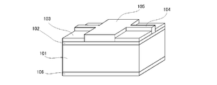
- Fig. 1 shows an overview of a general mass-produced solar cell using a single crystal or polycrystalline silicon substrate.
- a diffusion layer 102 is formed by diffusing a high concentration of impurities in a silicon substrate 101, and at the same time, a pn junction is formed.
- a plurality of collecting electrodes 105 are provided as electrodes for collecting the extraction electrodes and connecting the solar cells.
- a method for forming this electrode in view of cost, a method is widely used in which a metal paste in which fine metal particles such as Ag are mixed with an organic binder is printed using a screen plate, and is heat-treated at several hundred degrees to adhere to the substrate. It has been.
- a back electrode 106 having a polarity opposite to that of the light receiving surface is formed by screen printing of a metal paste in which metal fine particles such as Al are mixed with an organic binder and baking at about 700 to 850 ° C. .
- An antireflection film 103 for more efficiently capturing light is formed in a region where light enters the solar cell.
- the antireflection film a silicon nitride film formed by chemical vapor deposition or the like is widely used.
- the silicon atoms in the crystal are in a stable state because they are covalently bonded with adjacent atoms.
- an unstable energy level called a dangling bond or a dangling bond appears due to the absence of adjacent atoms to be bonded on the surface which is the terminal of the atomic arrangement. Since the dangling bond is electrically active, the charge generated in the silicon is captured and lost, and the characteristics of the solar cell are impaired. In order to suppress this loss, the solar cell is subjected to some surface termination treatment to reduce dangling bonds.
- etching paste printing to partially remove the passivation film to expose silicon, and then deposit or print metal from above.
- a metal film is formed on the passivation film, the metal is heated by irradiating the laser beam in a dot shape from the metal film, and a silicon / electrode contact is formed by penetrating the passivation film (for example, S. W. Glunz, R. Preu, S. Schaefer, E. Schneiderlochner, W. Pflegging, R. Ludemann, G. Willeke, Proc. The 28 IEEE v Photovoltaic.
- the formation of the narrow contact type and the point contact type is not only in the number of steps, but also requires a new resist material and etching paste for patterning, which is costly and sufficiently gains the effect of the passivation. I can't. Further, the method using a laser is expensive, and a complicated process such as vapor deposition is required for forming a metal film, so that the cost advantage is also reduced.
- the present invention has been made in view of the above circumstances, and can be manufactured at low cost in terms of low cost loss at the electrode / silicon interface, improved short circuit current and open voltage, improved solar cell characteristics, and cost.
- An object of the present invention is to provide a solar cell and a solar cell module.
- the present invention provides the following solar cell and solar cell module.
- a solar cell in which a passivation film is formed on a crystalline silicon substrate having at least a pn junction and an electrode is formed through printing and heat treatment processes of a conductive paste, an extraction electrode for extracting photogenerated carriers from the silicon substrate is silicon.
- a first electrode formed so as to be in contact with the substrate; and a second electrode formed such that a collecting electrode that collects carriers collected by the first electrode is in contact with the first electrode;
- the area ratio of the non-contact portion of the second electrode and the silicon substrate excluding the area where the first electrode and the second electrode are in contact is determined from the area determined by the width and total extension of the second electrode, [1] The solar cell according to [1], which is 20% or more with respect to an area excluding an area of a portion in contact with the second electrode. [3]: The solar cell according to [1] or [2], wherein the first electrode is in partial contact with the second electrode or is entirely overlapped. [4]: The first electrode is formed of a conductive paste containing a simple substance or compound of B, Al, Ga, P, As, In, and Sb, and the element is diffused at a high concentration in the lower portion of the silicon substrate.
- a solar cell module comprising the solar cells according to any one of [1] to [6] electrically connected thereto.
- the passivation film By leaving the passivation film completely or partially between the collector electrode and silicon, the charge loss at the electrode / silicon interface can be reduced, the short-circuit current and the open-circuit voltage can be improved, and the solar cell characteristics can be improved. . Further, the process can be realized by a conventional screen printing technique or the like, which is extremely effective for cost reduction.
- FIG. 1 It is the schematic perspective view which showed the structure of the general solar cell by a prior art. It is the schematic perspective view which showed an example of the structure of the general solar cell based on this invention. It is the schematic perspective view which showed the other example of the structure of the general solar cell based on this invention.
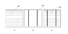
- (A) to (c) are plan views showing examples of printing plate making used for electrode formation according to the present invention, (a) is a pattern with only an extraction electrode, (b) is a pattern with only a collecting electrode, (c) Shows an example in which both the extraction electrode and the collector electrode are patterned. It is the graph which showed the influence on the solar cell characteristic based on this invention. It is the graph which showed the influence of the glass frit addition amount based on this invention. It is a figure explaining the passivation area under an electrode based on this invention.
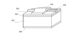
- FIG. 2 shows a solar cell according to an embodiment of the present invention.
- a pn junction is formed at the same time as a diffusion layer 202 is formed by diffusing impurities at a high concentration in a silicon substrate 201.
- a first electrode 204 formed so as to be in contact with the silicon substrate; and a second electrode 205 formed so that a collecting electrode for collecting carriers collected by the first electrode 204 is in contact with the first electrode 204.
- At least the second electrode 205 and the high-concentration diffusion layer 202 are only partially or wholly other than the contact point between the first electrode 204 and the second electrode 205. By not in contact, it is possible to silicon surface passivation under the second electrode 205.
- Reference numeral 206 denotes a back electrode.
- the area ratio of the non-contact portion between the second electrode and the silicon substrate excluding the area where the first electrode and the second electrode are in contact is first determined from the area determined by the width and total extension of the second electrode. It is preferably 20% or more, particularly 40 to 100% with respect to the area excluding the area where the electrode and the second electrode are in contact.
- the second electrode is preferably formed of a conductive paste having a glass frit content less than the glass frit content of the conductive paste used for the first electrode, and the second electrode contains a glass frit. It is preferably formed of a conductive paste having an amount of at least 2% by mass or less, preferably 1% by mass or less, and may be 0% by mass. In this case, the glass frit content of the conductive paste used for the first electrode is preferably 8 to 20% by mass, particularly 8 to 10% by mass. If it is less than 8% by mass, the contact with the high-concentration diffusion layer becomes insufficient, and the electrical resistance may increase and the characteristics of the solar cell may deteriorate.
- the amount is more than 20% by mass, the electrically insulating glass component becomes excessive, and the electrical conductivity of the electrode itself decreases, or the glass component excessively enters between the electrode and the high-concentration diffusion layer.
- the resistance may increase and the characteristics of the solar cell may deteriorate.
- the first electrode 204 is partially in contact with the second electrode 205, but as shown in FIG. 3, the entire first electrode 304 is overlapped with the second electrode 305.
- 301 is a silicon substrate
- 302 is a high concentration diffusion layer
- 303 is a passivation film
- 306 is a back electrode.
- the first electrode is formed of a conductive paste containing a simple substance or compound of B, Al, Ga, P, As, In, and Sb, and the element is diffused at a high concentration in the lower portion of the silicon substrate. It is preferable to have a region.
- the conductivity of the second electrode is preferably higher than the conductivity of the first electrode.
- the passivation film is preferably made of silicon oxide, silicon nitride, silicon carbide, aluminum oxide, amorphous silicon, microcrystalline silicon, titanium oxide, or a combination thereof.
- a collector electrode composed of a combination of the first electrode and the second electrode is formed on the light receiving surface, the non-light receiving surface, or both of the solar cell.
- the single crystal silicon substrate may be manufactured by either the CZ method or the FZ method.
- a single crystal ⁇ 100 ⁇ n-type silicon substrate having a resistivity of 0.1 to 5 ⁇ ⁇ cm by doping high purity silicon with a group V element such as P or Sb may be used.
- a group V element such as P or Sb
- Texture is an effective way to reduce solar cell reflectivity.
- the texture is 10 to 10 in an alkaline solution (concentration 1 to 10% by mass, temperature 60 to 100 ° C.) such as heated sodium hydroxide, potassium hydroxide, potassium carbonate, sodium carbonate, sodium hydrogen carbonate, tetramethylammonium hydroxide. It is easily produced by dipping for about 30 minutes. In many cases, a predetermined amount of 2-propanol is dissolved in the solution to control the reaction.
- the texture is formed, it is washed in an acidic aqueous solution of hydrochloric acid, sulfuric acid, nitric acid, hydrofluoric acid, or a mixture thereof.
- hydrochloric acid may be mixed with 0.5 to 5% by mass of hydrogen peroxide and heated to 60 to 90 ° C. for washing.
- a high concentration diffusion layer is formed by a vapor phase diffusion method using phosphorus oxychloride.
- the high concentration diffusion layer in the case of using an n-type substrate is formed by vapor phase diffusion of boron bromide.
- silicon solar cells it is necessary to form a pn junction only on the light-receiving surface side, and in order to achieve this, diffusion is performed in a state where two substrates are overlapped, or a diffusion layer on one side is formed with an alkaline aqueous solution or the like. It is necessary to devise such that the pn junction cannot be formed on the back surface by etching. After diffusion, the glass formed on the surface is removed with hydrofluoric acid or the like.
- an antireflection / passivation film for the light receiving surface is formed.
- a silicon nitride film or the like is formed to a thickness of about 100 nm using a chemical vapor deposition apparatus.
- the reaction gas monosilane (SiH 4 ) and ammonia (NH 3 ) are often mixed and used, but nitrogen can be used instead of NH 3 , and the film formation species can be diluted with H 2 gas. And adjusting the process pressure and diluting the reaction gas to achieve a desired refractive index.
- silicon oxide, silicon carbide, aluminum oxide, amorphous silicon, microcrystalline silicon, titanium oxide, or the like by a method such as heat treatment or atomic layer deposition may be used instead.
- the passivation film is not limited to a silicon nitride film, and as described above, silicon oxide, silicon carbide, aluminum oxide, amorphous silicon, microcrystalline silicon, titanium oxide, or a combination thereof may be used. obtain.
- FIG. 4 An Ag paste in which Ag powder and glass frit are mixed with an organic binder is printed, and thereafter, the Ag powder is passed through a passivation film such as a silicon nitride film by heat treatment to make the electrode and silicon conductive.
- 401 is a first electrode print pattern
- 402 is a second electrode print pattern.
- a high-concentration impurity diffusion layer may be formed in the silicon substrate under the first electrode.
- B or Al, Ga, P, As, In, or Sb or a compound in advance to the first electrode conductive paste, a high-concentration diffusion layer is formed on the silicon substrate simultaneously with firing after electrode printing.
- the maximum impurity concentration in a high-concentration impurity diffusion layer formed on a silicon substrate is generally 2 from the relationship between the work function of metal and silicon. ⁇ 10 19 atoms / cm 3 or more, and it is preferably adjusted to be 5 ⁇ 10 19 atoms / cm 3 or more. The upper limit is 2 ⁇ 10 22 atoms / cm 3 .
- the collector electrode corresponding to the second electrode is screen printed.
- the plate making of the second electrode may be a pattern having only the collector electrode as shown in FIG. 4B, or a pattern in which both the extraction electrode and the collector electrode are patterned as shown in FIG.
- One electrode may be overcoated. In the latter case, by making the conductivity of the second electrode higher than that of the first electrode, it is possible to reduce the resistance loss of the electrode and further improve the characteristics of the solar cell.
- the second electrode Ag paste in order to leave a passivation film other than the first electrode formation region, an additive adjusted so that the penetration performance of the passivation film is lower than that of the first electrode Ag paste is used.
- the passivation film penetration performance of the conductive paste can be controlled by the glass frit content in the conductive paste.
- Glass frit includes B—Pb—O, B—Si—Pb—O, B—Si—Pb—Al—O, B—Si—Bi—Pb—O, B—Si—Zn—O. It is preferable to use a glass material such as a system.
- the back electrode is formed by screen printing a paste in which Al powder is mixed with an organic binder. After printing, the back electrode and the second electrode are formed by baking at a temperature of 700 to 850 ° C. for 5 to 30 minutes. The back electrode and the light-receiving surface electrode can be baked at the same time. The order of forming the electrodes on each surface may be changed.
- the method for forming the electrode is not limited to screen printing, and a method such as dispenser or aerosol deposition is also possible.
- FIG. 5 shows the relationship between the area ratio of the passivation film remaining under the electrode and the open circuit voltage.
- the passivation film area ratio was an average value of 6 samples for each conductive paste condition, and the open circuit voltage was plotted as an average value, a maximum value, and a minimum value.
- the increase rate of the open-circuit voltage slowed down from the vicinity of the under-electrode passivation area of 20% and almost saturated at 40% or more. From this result, it can be said that the passivation area under the second electrode is preferably 20% or more, preferably 40% or more with respect to the electrode area.
- FIG. 6 shows the glass frit content of the Ag paste used in the above examination on the horizontal axis and the area ratio of the passivation film remaining under the second electrode on the vertical axis.
- the glass frit contents of the Ag paste with the passivation area under the second electrode of 20% and 40% were about 2% by mass and 1% by mass, respectively.
- FIG. 7 schematically shows the sample surface of the second electrode formation region in the solar battery cell after the electrode is dissolved.
- the passivation area is a portion 702 where the second electrode penetrates the passivation film 705 from the area excluding the portion 704 where the first electrode and the second electrode overlap each other (net second electrode area) inside the second electrode formation region 701. Is defined as the area minus the total area.
- the passivation area ratio is the ratio of the passivation area to the net second electrode area.
- the measurement of the passivation area can be performed by acquiring a surface image with a digital imager and processing the image.
- Examples and Comparative Examples In order to confirm the effectiveness of the present invention, as a comparative example, a power generation performance of a solar cell having a general electrode structure and a solar cell having an electrode structure of the present invention was compared. After removing a damaged layer with a hot concentrated potassium hydroxide aqueous solution on 100 boron-doped ⁇ 100 ⁇ p-type ascut silicon substrates having a diffusion thickness of 250 ⁇ m and a specific resistance of 1 ⁇ ⁇ cm, Immersion and texture formation were followed by washing in a hydrochloric acid / hydrogen peroxide mixed solution.
- an Al paste was screen printed on the entire back side of all the substrates and dried. Thereafter, baking at 780 ° C. was performed in an air atmosphere, and the silicon nitride film was passed through the Ag electrode to conduct with silicon, and at the same time, the Al electrode on the back surface of the substrate was made to conduct with silicon.
- the entire electrode surface was electrically connected to silicon, and the non-contact area between the electrode and silicon was 0%.
- the plate making shown in FIG. 4C was used and formed so as to overlap with the first electrode.
- the amount of glass frit added was adjusted so that the non-contact area between the second electrode and silicon was 80%, and an Ag paste formulated to have a higher conductivity than the first electrode was applied by screen printing, and then 750 A heat treatment at 0 ° C. was performed in an air atmosphere to be cured. Since A has the same thermal history as B, heat treatment was performed at 750 ° C. in an air atmosphere in the same firing furnace as B.
- the characteristics of the solar cells A and B were measured with a current-voltage measuring machine using artificial sunlight with an air mass of 1.5, as shown in Table 1, the characteristics of B implementing the present invention were A The results superior to the characteristics of were obtained.
Landscapes
- Photovoltaic Devices (AREA)
- Electrodes Of Semiconductors (AREA)
- Life Sciences & Earth Sciences (AREA)
- Chemical & Material Sciences (AREA)
- Crystallography & Structural Chemistry (AREA)
- Sustainable Development (AREA)
Abstract
Priority Applications (9)
| Application Number | Priority Date | Filing Date | Title |
|---|---|---|---|
| RU2013131017/28A RU2571167C2 (ru) | 2010-12-06 | 2011-12-01 | Солнечный элемент и модуль солнечного элемента |
| SG2013043849A SG191045A1 (en) | 2010-12-06 | 2011-12-01 | Solar cell and solar-cell module |
| PH1/2013/501161A PH12013501161A1 (en) | 2010-12-06 | 2011-12-01 | Solar cell and solar-cell module |
| CN201180065726.8A CN103329279B (zh) | 2010-12-06 | 2011-12-01 | 太阳能电池和太阳能电池模件 |
| KR1020137017730A KR101847470B1 (ko) | 2010-12-06 | 2011-12-01 | 태양전지 및 태양전지 모듈 |
| CA2820034A CA2820034A1 (fr) | 2010-12-06 | 2011-12-01 | Cellule solaire et module cellule solaire |
| US13/992,015 US9224888B2 (en) | 2010-12-06 | 2011-12-01 | Solar cell and solar-cell module |
| EP11847500.3A EP2650926B1 (fr) | 2010-12-06 | 2011-12-01 | Cellule solaire et procédé de fabrication de cellule solaire |
| JP2012547810A JP5626361B2 (ja) | 2010-12-06 | 2011-12-01 | 太陽電池及び太陽電池モジュール、並びに太陽電池の製造方法 |
Applications Claiming Priority (2)
| Application Number | Priority Date | Filing Date | Title |
|---|---|---|---|
| JP2010271659 | 2010-12-06 | ||
| JP2010-271659 | 2010-12-06 |
Publications (1)
| Publication Number | Publication Date |
|---|---|
| WO2012077568A1 true WO2012077568A1 (fr) | 2012-06-14 |
Family
ID=46207058
Family Applications (1)
| Application Number | Title | Priority Date | Filing Date |
|---|---|---|---|
| PCT/JP2011/077787 Ceased WO2012077568A1 (fr) | 2010-12-06 | 2011-12-01 | Cellule solaire et module cellule solaire |
Country Status (12)
| Country | Link |
|---|---|
| US (1) | US9224888B2 (fr) |
| EP (1) | EP2650926B1 (fr) |
| JP (1) | JP5626361B2 (fr) |
| KR (1) | KR101847470B1 (fr) |
| CN (1) | CN103329279B (fr) |
| CA (1) | CA2820034A1 (fr) |
| MY (1) | MY164543A (fr) |
| PH (1) | PH12013501161A1 (fr) |
| RU (1) | RU2571167C2 (fr) |
| SG (1) | SG191045A1 (fr) |
| TW (1) | TWI521724B (fr) |
| WO (1) | WO2012077568A1 (fr) |
Cited By (6)
| Publication number | Priority date | Publication date | Assignee | Title |
|---|---|---|---|---|
| JP2013004831A (ja) * | 2011-06-20 | 2013-01-07 | Sharp Corp | 結晶太陽電池セルおよび結晶太陽電池セルの製造方法 |
| JP2013048306A (ja) * | 2012-12-07 | 2013-03-07 | Sharp Corp | 結晶太陽電池セル |
| JP2015130406A (ja) * | 2014-01-07 | 2015-07-16 | 三菱電機株式会社 | 光起電力装置およびその製造方法、光起電力モジュール |
| JP2016092238A (ja) * | 2014-11-05 | 2016-05-23 | 信越化学工業株式会社 | 太陽電池及びその製造方法 |
| JPWO2017119036A1 (ja) * | 2016-01-05 | 2018-10-04 | パナソニックIpマネジメント株式会社 | 太陽電池モジュール |
| JP7075535B1 (ja) | 2021-08-27 | 2022-05-25 | 上海晶科緑能企業管理有限公司 | 光起電力電池セル、電池モジュール及び製造プロセス |
Families Citing this family (12)
| Publication number | Priority date | Publication date | Assignee | Title |
|---|---|---|---|---|
| KR102018652B1 (ko) * | 2012-08-29 | 2019-09-05 | 엘지전자 주식회사 | 태양 전지 |
| KR101867855B1 (ko) | 2014-03-17 | 2018-06-15 | 엘지전자 주식회사 | 태양 전지 |
| JP6219913B2 (ja) * | 2014-11-28 | 2017-10-25 | エルジー エレクトロニクス インコーポレイティド | 太陽電池及びその製造方法 |
| JP7064823B2 (ja) * | 2016-08-31 | 2022-05-11 | 株式会社マテリアル・コンセプト | 太陽電池及びその製造方法 |
| CN108074999A (zh) * | 2016-11-16 | 2018-05-25 | 镇江大全太阳能有限公司 | 一种选择性发射极黑硅电池及其制作方法 |
| RU172396U1 (ru) * | 2016-12-28 | 2017-07-06 | Федеральное государственное бюджетное учреждение науки Физико-технический институт им. А.Ф. Иоффе Российской академии наук | Солнечный элемент |
| WO2018174898A1 (fr) | 2017-03-24 | 2018-09-27 | Heraeus Precious Metals North America Conshohocken Llc | Verres à faible gravure et sans contact pour compositions de pâte électroconductrice |
| CN109065639A (zh) * | 2018-06-22 | 2018-12-21 | 晶澳(扬州)太阳能科技有限公司 | N型晶体硅太阳能电池及制备方法、光伏组件 |
| CN112786734A (zh) * | 2019-11-08 | 2021-05-11 | 泰州隆基乐叶光伏科技有限公司 | 太阳能电池组件生产方法及太阳能电池组件 |
| CN114284381A (zh) * | 2020-09-18 | 2022-04-05 | 嘉兴阿特斯技术研究院有限公司 | 异质结太阳能电池及其制作方法 |
| CN113921622B (zh) * | 2021-09-30 | 2024-04-05 | 中国科学院苏州纳米技术与纳米仿生研究所 | 电池片基板、光伏电池、光伏电池组件及其组装方法 |
| CN115579423B (zh) * | 2022-10-19 | 2024-07-09 | 通威太阳能(安徽)有限公司 | 丝网印刷不良电池片的处理方法 |
Citations (6)
| Publication number | Priority date | Publication date | Assignee | Title |
|---|---|---|---|---|
| JPH11512886A (ja) * | 1995-10-05 | 1999-11-02 | エバラ・ソーラー・インコーポレーテッド | 自己整列的に部分的に深く拡散したエミッタの太陽電池 |
| JP2004273826A (ja) * | 2003-03-10 | 2004-09-30 | Sharp Corp | 光電変換装置及びその製造方法 |
| JP2006156693A (ja) * | 2004-11-29 | 2006-06-15 | Kyocera Corp | 太陽電池素子及び、これを用いた太陽電池モジュール |
| JP2007096040A (ja) * | 2005-09-29 | 2007-04-12 | Sharp Corp | 太陽電池の製造方法および太陽電池 |
| WO2009128679A2 (fr) * | 2008-04-17 | 2009-10-22 | Lg Electronics Inc. | Cellule solaire, procédé de formation de couche émettrice de cellule solaire, et procédé de fabrication de cellule solaire |
| JP2009295715A (ja) * | 2008-06-04 | 2009-12-17 | Sharp Corp | 光電変換装置およびその製造方法 |
Family Cites Families (25)
| Publication number | Priority date | Publication date | Assignee | Title |
|---|---|---|---|---|
| RU1648224C (ru) * | 1988-12-20 | 1995-01-09 | Научно-производственное предприятие "Сатурн" | Способ изготовления фотопреобразователя |
| JPH0536998A (ja) | 1991-07-30 | 1993-02-12 | Sharp Corp | 電極の形成方法 |
| JP2928433B2 (ja) * | 1993-02-23 | 1999-08-03 | シャープ株式会社 | 光電変換素子の製造方法 |
| JP2000138386A (ja) | 1998-11-04 | 2000-05-16 | Shin Etsu Chem Co Ltd | 太陽電池の製造方法およびこの方法で製造された太陽電池 |
| US6632730B1 (en) | 1999-11-23 | 2003-10-14 | Ebara Solar, Inc. | Method for self-doping contacts to a semiconductor |
| RU2274615C2 (ru) | 2000-04-28 | 2006-04-20 | Мерк Патент Гмбх | Гравировальные пасты для неорганических поверхностей |
| JP2002217434A (ja) * | 2001-01-19 | 2002-08-02 | Sharp Corp | 太陽電池、太陽電池用インターコネクターおよびストリング |
| JP4121928B2 (ja) | 2003-10-08 | 2008-07-23 | シャープ株式会社 | 太陽電池の製造方法 |
| JP4557622B2 (ja) | 2004-07-29 | 2010-10-06 | 京セラ株式会社 | 太陽電池素子の接続構造及びこれを含む太陽電池モジュール |
| JP2008204967A (ja) | 2005-05-31 | 2008-09-04 | Naoetsu Electronics Co Ltd | 太陽電池素子及びその製造方法 |
| US7765949B2 (en) * | 2005-11-17 | 2010-08-03 | Palo Alto Research Center Incorporated | Extrusion/dispensing systems and methods |
| JP4963866B2 (ja) | 2006-04-28 | 2012-06-27 | シャープ株式会社 | 光電変換素子の製造方法 |
| TWI487124B (zh) | 2006-08-25 | 2015-06-01 | Sanyo Electric Co | 太陽電池模組及太陽電池模組的製造方法 |
| EP2109149A4 (fr) * | 2007-01-25 | 2011-04-20 | Sharp Kk | Cellule de batterie solaire, reseau de batteries solaires, module de batterie solaire et procede de fabrication d'un reseau de batteries solaires |
| CN101743640B (zh) * | 2007-07-26 | 2012-12-19 | 康斯坦茨大学 | 具有回蚀刻发射极的硅太阳能电池的制造方法和相应的太阳能电池 |
| RU2357325C1 (ru) * | 2007-10-29 | 2009-05-27 | Российская академия Сельскохозяйственных наук Государственное научное учреждение Всероссийский научно-исследовательский институт электрификации сельского хозяйства (ГНУ ВИЭСХ) | Полупроводниковый фотоэлектрический генератор и способ его изготовления |
| JP4610630B2 (ja) | 2008-03-31 | 2011-01-12 | 三菱電機株式会社 | 太陽電池用拡散層の製造方法および太陽電池セルの製造方法 |
| US20090250108A1 (en) | 2008-04-02 | 2009-10-08 | Applied Materials, Inc. | Silicon carbide for crystalline silicon solar cell surface passivation |
| KR100994924B1 (ko) * | 2008-04-17 | 2010-11-19 | 엘지전자 주식회사 | 태양전지 및 그 제조방법 |
| TWI423462B (zh) * | 2008-10-22 | 2014-01-11 | Ind Tech Res Inst | 矽晶太陽電池之背面電極製造方法 |
| KR100993511B1 (ko) | 2008-11-19 | 2010-11-12 | 엘지전자 주식회사 | 태양 전지 및 그 제조 방법 |
| KR101002282B1 (ko) | 2008-12-15 | 2010-12-20 | 엘지전자 주식회사 | 태양 전지 및 그 제조 방법 |
| JP2010251343A (ja) * | 2009-04-10 | 2010-11-04 | Mitsubishi Electric Corp | 太陽電池およびその製造方法 |
| US8722453B2 (en) | 2009-04-14 | 2014-05-13 | Mitsubishi Electric Corporation | Photovoltaic device and method for manufacturing the same |
| US8586129B2 (en) * | 2010-09-01 | 2013-11-19 | Solarworld Innovations Gmbh | Solar cell with structured gridline endpoints and vertices |
-
2011
- 2011-12-01 CA CA2820034A patent/CA2820034A1/fr not_active Abandoned
- 2011-12-01 PH PH1/2013/501161A patent/PH12013501161A1/en unknown
- 2011-12-01 RU RU2013131017/28A patent/RU2571167C2/ru active
- 2011-12-01 WO PCT/JP2011/077787 patent/WO2012077568A1/fr not_active Ceased
- 2011-12-01 CN CN201180065726.8A patent/CN103329279B/zh active Active
- 2011-12-01 US US13/992,015 patent/US9224888B2/en active Active
- 2011-12-01 SG SG2013043849A patent/SG191045A1/en unknown
- 2011-12-01 EP EP11847500.3A patent/EP2650926B1/fr active Active
- 2011-12-01 KR KR1020137017730A patent/KR101847470B1/ko active Active
- 2011-12-01 JP JP2012547810A patent/JP5626361B2/ja active Active
- 2011-12-01 MY MYPI2013002040A patent/MY164543A/en unknown
- 2011-12-06 TW TW100144863A patent/TWI521724B/zh active
Patent Citations (6)
| Publication number | Priority date | Publication date | Assignee | Title |
|---|---|---|---|---|
| JPH11512886A (ja) * | 1995-10-05 | 1999-11-02 | エバラ・ソーラー・インコーポレーテッド | 自己整列的に部分的に深く拡散したエミッタの太陽電池 |
| JP2004273826A (ja) * | 2003-03-10 | 2004-09-30 | Sharp Corp | 光電変換装置及びその製造方法 |
| JP2006156693A (ja) * | 2004-11-29 | 2006-06-15 | Kyocera Corp | 太陽電池素子及び、これを用いた太陽電池モジュール |
| JP2007096040A (ja) * | 2005-09-29 | 2007-04-12 | Sharp Corp | 太陽電池の製造方法および太陽電池 |
| WO2009128679A2 (fr) * | 2008-04-17 | 2009-10-22 | Lg Electronics Inc. | Cellule solaire, procédé de formation de couche émettrice de cellule solaire, et procédé de fabrication de cellule solaire |
| JP2009295715A (ja) * | 2008-06-04 | 2009-12-17 | Sharp Corp | 光電変換装置およびその製造方法 |
Non-Patent Citations (3)
| Title |
|---|
| J. KNOBLOCH; A. NOEL; E. SCHAFFER; U. SCHUBERT; F. J. KAMEREWERD; S. KLUSSMANN; W. WETTLING, PROC. THE 23RD IEEE PHOTOVOLTAIC SPECIALISTS CONFERENCE, 1993, pages 271 |
| S. W. GLUNZ; R. PREU; S. SCHAEFER; E. SCHNEIDERLOCHNER; W. PFLEGING; R. LUDEMANN; G. WILLEKE, PROC. THE 28TH IEEE PHOTOVOLTAIC SHEPCIALISTS CONFERENCE, 2000, pages 168 |
| See also references of EP2650926A4 |
Cited By (9)
| Publication number | Priority date | Publication date | Assignee | Title |
|---|---|---|---|---|
| JP2013004831A (ja) * | 2011-06-20 | 2013-01-07 | Sharp Corp | 結晶太陽電池セルおよび結晶太陽電池セルの製造方法 |
| JP2013048306A (ja) * | 2012-12-07 | 2013-03-07 | Sharp Corp | 結晶太陽電池セル |
| JP2015130406A (ja) * | 2014-01-07 | 2015-07-16 | 三菱電機株式会社 | 光起電力装置およびその製造方法、光起電力モジュール |
| JP2016092238A (ja) * | 2014-11-05 | 2016-05-23 | 信越化学工業株式会社 | 太陽電池及びその製造方法 |
| JPWO2017119036A1 (ja) * | 2016-01-05 | 2018-10-04 | パナソニックIpマネジメント株式会社 | 太陽電池モジュール |
| JP7075535B1 (ja) | 2021-08-27 | 2022-05-25 | 上海晶科緑能企業管理有限公司 | 光起電力電池セル、電池モジュール及び製造プロセス |
| JP2023033059A (ja) * | 2021-08-27 | 2023-03-09 | 上海晶科緑能企業管理有限公司 | 光起電力電池セル、電池モジュール及び製造プロセス |
| US11764313B2 (en) | 2021-08-27 | 2023-09-19 | Shanghai Jinko Green Energy Enterprise Management Co., Ltd. | Photovoltaic solar cell, solar cell module and manufacturing process |
| US12446355B2 (en) | 2021-08-27 | 2025-10-14 | Shanghai Jinko Green Energy Enterprise Management Co., Ltd. | Photovoltaic solar cell, solar cell module and manufacturing process |
Also Published As
| Publication number | Publication date |
|---|---|
| RU2571167C2 (ru) | 2015-12-20 |
| RU2013131017A (ru) | 2015-01-20 |
| CN103329279A (zh) | 2013-09-25 |
| EP2650926A1 (fr) | 2013-10-16 |
| PH12013501161A1 (en) | 2013-07-29 |
| CN103329279B (zh) | 2016-11-02 |
| JP5626361B2 (ja) | 2014-11-19 |
| TWI521724B (zh) | 2016-02-11 |
| US20130255747A1 (en) | 2013-10-03 |
| KR101847470B1 (ko) | 2018-04-10 |
| MY164543A (en) | 2018-01-15 |
| EP2650926B1 (fr) | 2021-03-31 |
| KR20130140106A (ko) | 2013-12-23 |
| US9224888B2 (en) | 2015-12-29 |
| JPWO2012077568A1 (ja) | 2014-05-19 |
| TW201236171A (en) | 2012-09-01 |
| CA2820034A1 (fr) | 2012-06-14 |
| SG191045A1 (en) | 2013-08-30 |
| EP2650926A4 (fr) | 2017-11-22 |
Similar Documents
| Publication | Publication Date | Title |
|---|---|---|
| JP5626361B2 (ja) | 太陽電池及び太陽電池モジュール、並びに太陽電池の製造方法 | |
| US11538944B2 (en) | Solar cell, method for manufacturing solar cell, and solar cell module | |
| JP5541370B2 (ja) | 太陽電池の製造方法、太陽電池及び太陽電池モジュール | |
| US20100084009A1 (en) | Solar Cells | |
| US20160197207A1 (en) | Solar cell, solar cell module, and manufacturing method of solar cell | |
| KR20130092494A (ko) | 태양 전지의 제조 방법 및 태양 전지 | |
| JP6405292B2 (ja) | 太陽電池の製造方法及び太陽電池 | |
| Hörteis et al. | Fine line printed and plated contacts on high ohmic emitters enabling 20% cell efficiency | |
| JP5316491B2 (ja) | 太陽電池の製造方法 | |
| JP5994895B2 (ja) | 太陽電池の製造方法 | |
| JP2013149815A (ja) | 太陽電池及びその製造方法 | |
| JP2003282907A (ja) | 太陽電池素子 |
Legal Events
| Date | Code | Title | Description |
|---|---|---|---|
| 121 | Ep: the epo has been informed by wipo that ep was designated in this application |
Ref document number: 11847500 Country of ref document: EP Kind code of ref document: A1 |
|
| ENP | Entry into the national phase |
Ref document number: 2012547810 Country of ref document: JP Kind code of ref document: A |
|
| ENP | Entry into the national phase |
Ref document number: 2820034 Country of ref document: CA |
|
| NENP | Non-entry into the national phase |
Ref country code: DE |
|
| WWE | Wipo information: entry into national phase |
Ref document number: 13992015 Country of ref document: US Ref document number: 12013501161 Country of ref document: PH |
|
| ENP | Entry into the national phase |
Ref document number: 20137017730 Country of ref document: KR Kind code of ref document: A |
|
| ENP | Entry into the national phase |
Ref document number: 2013131017 Country of ref document: RU Kind code of ref document: A |