WO2012081237A1 - Dispositif à semi-conducteur et son procédé de commande - Google Patents
Dispositif à semi-conducteur et son procédé de commande Download PDFInfo
- Publication number
- WO2012081237A1 WO2012081237A1 PCT/JP2011/006961 JP2011006961W WO2012081237A1 WO 2012081237 A1 WO2012081237 A1 WO 2012081237A1 JP 2011006961 W JP2011006961 W JP 2011006961W WO 2012081237 A1 WO2012081237 A1 WO 2012081237A1
- Authority
- WO
- WIPO (PCT)
- Prior art keywords
- gate electrode
- current
- ohmic
- electrode
- voltage
- Prior art date
- Legal status (The legal status is an assumption and is not a legal conclusion. Google has not performed a legal analysis and makes no representation as to the accuracy of the status listed.)
- Ceased
Links
Images


Classifications
-
- H—ELECTRICITY
- H10—SEMICONDUCTOR DEVICES; ELECTRIC SOLID-STATE DEVICES NOT OTHERWISE PROVIDED FOR
- H10D—INORGANIC ELECTRIC SEMICONDUCTOR DEVICES
- H10D30/00—Field-effect transistors [FET]
- H10D30/40—FETs having zero-dimensional [0D], one-dimensional [1D] or two-dimensional [2D] charge carrier gas channels
- H10D30/47—FETs having zero-dimensional [0D], one-dimensional [1D] or two-dimensional [2D] charge carrier gas channels having two-dimensional [2D] charge carrier gas channels, e.g. nanoribbon FETs or high electron mobility transistors [HEMT]
- H10D30/471—High electron mobility transistors [HEMT] or high hole mobility transistors [HHMT]
- H10D30/475—High electron mobility transistors [HEMT] or high hole mobility transistors [HHMT] having wider bandgap layer formed on top of lower bandgap active layer, e.g. undoped barrier HEMTs such as i-AlGaN/GaN HEMTs
-
- H—ELECTRICITY
- H10—SEMICONDUCTOR DEVICES; ELECTRIC SOLID-STATE DEVICES NOT OTHERWISE PROVIDED FOR
- H10D—INORGANIC ELECTRIC SEMICONDUCTOR DEVICES
- H10D62/00—Semiconductor bodies, or regions thereof, of devices having potential barriers
- H10D62/10—Shapes, relative sizes or dispositions of the regions of the semiconductor bodies; Shapes of the semiconductor bodies
- H10D62/17—Semiconductor regions connected to electrodes not carrying current to be rectified, amplified or switched, e.g. channel regions
- H10D62/343—Gate regions of field-effect devices having PN junction gates
-
- H—ELECTRICITY
- H10—SEMICONDUCTOR DEVICES; ELECTRIC SOLID-STATE DEVICES NOT OTHERWISE PROVIDED FOR
- H10D—INORGANIC ELECTRIC SEMICONDUCTOR DEVICES
- H10D62/00—Semiconductor bodies, or regions thereof, of devices having potential barriers
- H10D62/80—Semiconductor bodies, or regions thereof, of devices having potential barriers characterised by the materials
- H10D62/85—Semiconductor bodies, or regions thereof, of devices having potential barriers characterised by the materials being Group III-V materials, e.g. GaAs
- H10D62/8503—Nitride Group III-V materials, e.g. AlN or GaN
Definitions
- the present invention relates to a semiconductor device and a control method thereof, and more particularly, to a semiconductor device including a semiconductor element capable of flowing a current bidirectionally and a control method thereof.
- a wide gap semiconductor such as a group III nitride semiconductor represented by GaN or silicon carbide (SiC) has been studied.
- a wide gap semiconductor has a dielectric breakdown electric field about an order of magnitude higher than that of silicon (Si).
- AlGaN aluminum gallium nitride
- GaN gallium nitride
- 2DEG high mobility two-dimensional electron gas
- a bidirectional semiconductor device can be formed with a single semiconductor device (see, for example, Patent Document 1). .
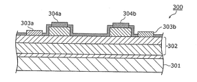
- FIG. 8 is a diagram showing a configuration of a conventional semiconductor element 300 described in Patent Document 1.
- a conventional semiconductor element 300 includes a substrate 301, a semiconductor layer stack 302, a first electrode 303a, a second electrode 303b, a first gate electrode 304a, and a second gate electrode 304b. Is provided.
- the semiconductor element 300 causes the power supply voltage to be reduced between the first electrode 303a and the second electrode 303b via the channel.
- a current can flow in a direction corresponding to the polarity.
- the conventional semiconductor device has a problem that power consumption increases.
- a first gate current flows from the first gate electrode toward the channel region immediately below the first gate electrode.
- a second gate current flows from the second gate electrode toward the channel region immediately below the second gate electrode.
- the potential of the second gate electrode is higher than the second electrode by the potential difference VGb between the second gate electrode and the second electrode, and higher than the first electrode by the sum of the power supply voltage VSba and the potential difference VGb. .
- the second gate current flows not only through the second electrode but also through the first electrode.
- the semiconductor device When the semiconductor device is in a conductive state and the power supply voltage VSba increases, the potential difference between the second gate electrode and the first electrode increases. For this reason, the second gate current increases as the power supply voltage VSba increases. Therefore, the driving power for driving the second gate electrode is increased.
- the present invention has been made to solve the above-described problems, and an object thereof is to provide a semiconductor device that can suppress an increase in power consumption and a driving method thereof.
- a semiconductor device is a semiconductor device including a semiconductor element that can flow a current bidirectionally, and the semiconductor element is formed over the substrate and the substrate And a pair of ohmic electrodes formed on or above the semiconductor layer and spaced apart from each other, and between the pair of ohmic electrodes on or above the semiconductor layer.
- a pair of gate electrodes corresponding to each of the pair of ohmic electrodes, and the semiconductor device further bi-directionally passes the semiconductor element between the pair of ohmic electrodes via the channel region.
- a control unit configured to make a conductive state in which a current can flow; and when the semiconductor element is in the conductive state, the control unit is configured to be a high one of the pair of ohmic electrodes.
- the potential of the high-potential side gate electrode which is a potential corresponding to the high-potential-side ohmic electrode
- a first electric signal is supplied to the high potential side gate electrode so as to be lower than the potential of the low potential side gate electrode which is a gate electrode corresponding to the low potential side ohmic electrode, and A second electric signal is supplied to the low potential side gate electrode.
- the magnitude of the gate current flowing through the high potential side gate electrode depends on the potential difference between the high potential side ohmic electrode and the high potential side gate electrode. Increase is suppressed and power consumption can be reduced.
- the magnitude of the saturation current of the current flowing between the pair of ohmic electrodes depends on the potential difference between the low-potential side ohmic electrode and the low-potential side gate electrode. The magnitude of the current can be maintained. Therefore, power consumption can be reduced while maintaining the characteristics of the power supply current and the power supply voltage.
- control unit includes a first voltage source that generates a first voltage that is equal to or higher than a threshold voltage of the pair of gate electrodes, and a second voltage source that generates a second voltage higher than the first voltage. And the control unit supplies the first voltage as the first electric signal to the high potential side gate electrode, and supplies the second voltage as the second electric signal to the low potential side gate electrode. Also good.
- a high voltage or a low voltage can be easily supplied between each gate electrode and the corresponding ohmic electrode. Accordingly, since the current flowing from the high potential side gate electrode to the channel region can be reduced while maintaining the characteristics of the power supply current and the power supply voltage, the driving power of the high potential side gate electrode can be suppressed.
- the control unit may include a first current source that generates a first current for applying a voltage that is equal to or higher than a threshold voltage of the pair of gate electrodes, and a second current that generates a second current larger than the first current. And the controller supplies the first current to the high potential side gate electrode as the first electrical signal and supplies the second current to the low potential side gate electrode as the second electrical signal. May be.
- the control unit may supply a current for applying a voltage equal to or higher than a threshold voltage of the pair of gate electrodes to the pair of gate electrodes as the first electric signal and the second electric signal.
- the threshold voltage of the pair of gate electrodes may be positive.
- the semiconductor element can be in a cut-off state.
- the semiconductor element may further include a pair of control layers having P-type conductivity formed between the pair of gate electrodes and the semiconductor layer.
- the threshold voltage of the first gate electrode and the threshold voltage of the second gate electrode can be made positive.
- the pair of gate electrodes may be in Schottky junction with the semiconductor layer.
- the threshold voltage of the first gate electrode and the threshold voltage of the second gate electrode can be made positive.
- the semiconductor element may further include an insulating film formed between the pair of gate electrodes and the semiconductor layer.
- the threshold voltage of the first gate electrode and the threshold voltage of the second gate electrode can be made positive.
- the substrate may be a silicon substrate, a sapphire substrate, or a silicon carbide substrate.
- a method for controlling a semiconductor device is a method for controlling a semiconductor device in which current can flow in both directions.
- the semiconductor device is formed over a substrate, the channel, and a channel.
- a pair of gate electrodes corresponding to each of the pair of ohmic electrodes, and the method of controlling the semiconductor device includes a high potential side gate which is a gate electrode corresponding to a high potential side ohmic electrode of the pair of ohmic electrodes
- a first electric signal is supplied to the electrode, and a second electric signal is applied to the low potential side gate electrode which is a gate electrode corresponding to the low potential side ohmic electrode of the pair of ohmic electrodes.
- the potential of the high potential side gate electrode when the high potential side ohmic electrode is used as a reference is the low potential side ohmic electrode
- the first electric signal and the second electric signal are supplied so as to be lower than the potential of the low-potential side gate electrode with reference to.
- the magnitude of the gate current flowing through the high potential side gate electrode depends on the potential difference between the high potential side ohmic electrode and the high potential side gate electrode. Increase is suppressed and power consumption can be reduced.
- the magnitude of the saturation current of the current flowing between the pair of ohmic electrodes depends on the potential difference between the low-potential side ohmic electrode and the low-potential side gate electrode. The magnitude of the current can be maintained. Therefore, power consumption can be reduced while maintaining the characteristics of the power supply current and the power supply voltage.
- the semiconductor device according to the present invention can suppress an increase in power consumption.
- FIG. 1A is a cross-sectional view showing an example of the configuration of the semiconductor device according to Embodiment 1 of the present invention.
- FIG. 1B is a cross-sectional view showing an example of the configuration of the semiconductor device according to Embodiment 1 of the present invention.
- FIG. 2 is a diagram for explaining the behavior of the channel region in the semiconductor device according to the first embodiment of the present invention.
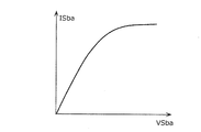
- FIG. 3A is a diagram showing an example of the relationship between the power supply current ISba and the power supply voltage VSba according to Embodiment 1 of the present invention.
- FIG. 3B is a diagram showing an example of the relationship between the gate current IGb and the power supply voltage VSba according to Embodiment 1 of the present invention.
- FIG. 4 is a cross-sectional view showing an example of the configuration of the semiconductor device according to the first modification of the first embodiment of the present invention.
- FIG. 5 is a cross-sectional view showing an example of the configuration of the semiconductor device according to Modification 2 of Embodiment 1 of the present invention.
- FIG. 6 is a cross-sectional view showing an example of the configuration of the semiconductor device according to the second embodiment of the present invention.
- FIG. 7 is a cross-sectional view showing an example of the configuration of a semiconductor device according to a variation of the second embodiment of the present invention.
- FIG. 8 is a cross-sectional view showing a configuration of a conventional semiconductor element.
- a semiconductor device includes a semiconductor element having a pair of gate electrodes and a pair of ohmic electrodes, and applying a voltage higher than a threshold voltage to the pair of gate electrodes. And a control unit for bringing the ohmic electrodes into a conductive state.
- the control unit applies a low voltage to the gate electrode corresponding to the high-potential side ohmic electrode and applies a high voltage to the gate electrode corresponding to the low-potential side ohmic electrode when the semiconductor element is in a conductive state. It is characterized by doing.
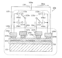
- FIGS. 1A and 1B are cross-sectional views showing an example of the configuration of the semiconductor device 10 according to the first embodiment of the present invention.
- the semiconductor device 10 includes a semiconductor element 100 and a control unit 120.
- the semiconductor element 100 can flow a current bidirectionally according to the polarity of the power supply voltage VSba of the power supply 130.
- a semiconductor element 100 includes a substrate 101, a semiconductor layer stack 102, a first ohmic electrode 104a, a second ohmic electrode 104b, a first gate electrode 105a, and a second gate.
- the electrode 105b, the first ohmic terminal 106a, the second ohmic terminal 106b, the first gate terminal 107a, the second gate terminal 107b, the first control layer 108a, and the second control layer 108b are provided.
- the substrate 101 is, for example, a semiconductor substrate such as silicon (Si).
- the substrate 101 may be a sapphire substrate or a silicon carbide (SiC) substrate.
- the semiconductor layer stack 102 is formed on the substrate 101 and has a channel region 103.
- the semiconductor layer stack 102 is made of, for example, GaN / AlGaN.
- the first ohmic electrode 104a and the second ohmic electrode 104b are a pair of ohmic electrodes formed on or above the semiconductor layer stack 102 so as to be separated from each other.
- the first ohmic electrode 104a and the second ohmic electrode 104b have, for example, a stacked structure of titanium (Ti) and aluminum (Al).
- the first gate electrode 105a is one of a pair of gate electrodes formed between the pair of ohmic electrodes on or above the semiconductor layer stack 102. Specifically, the first gate electrode 105a is formed between the first ohmic electrode 104a and the second ohmic electrode 104b.
- the first gate electrode 105a corresponds to one of a pair of ohmic electrodes. Specifically, the first gate electrode 105a corresponds to the first ohmic electrode 104a, and is formed in a region closer to the first ohmic electrode 104a than the second ohmic electrode 104b.
- the first gate electrode 105a is made of nickel (Ni), for example.
- the ohmic electrode and the gate electrode corresponding to the ohmic electrode are a pair of electrodes to which a voltage for forming a channel in the channel region 103 is applied.
- the first gate electrode 105a corresponding to the first ohmic electrode 104a is supplied with a potential higher than the threshold voltage of the first gate electrode 105a, which is a potential when the first ohmic electrode 104a is used as a reference. In this case, a channel is generated in the channel region 103 below the first gate electrode 105a.
- the threshold voltage of the first gate electrode 105a is positive, for example.
- the second gate electrode 105b is the other of the pair of gate electrodes formed between the pair of ohmic electrodes on or above the semiconductor layer stack 102. Specifically, the second gate electrode 105b is formed between the first gate electrode 105a and the second ohmic electrode 104b.
- the second gate electrode 105b corresponds to the other of the pair of ohmic electrodes. Specifically, the second gate electrode 105b corresponds to the second ohmic electrode 104b, and is formed in a region closer to the second ohmic electrode 104b than the first ohmic electrode 104a.
- the second gate electrode 105b is made of nickel, for example.
- the second gate electrode 105b corresponding to the second ohmic electrode 104b has a potential when the second ohmic electrode 104b is used as a reference and is equal to or higher than the threshold voltage of the second gate electrode 105b.
- a channel is generated in the channel region 103 below the second gate electrode 105b.
- the threshold voltage of the second gate electrode 105b is positive, for example.
- the first ohmic terminal 106a is connected to the first ohmic electrode 104a.
- the first ohmic terminal 106 a is a terminal for connecting a voltage source (or current source) included in the control unit 120 and the power source 130.
- the second ohmic terminal 106b is connected to the second ohmic electrode 104b.
- the second ohmic terminal 106 b is a terminal for connecting a voltage source (or current source) included in the control unit 120 and the power source 130.
- the first gate terminal 107a is connected to the first gate electrode 105a.
- the first gate terminal 107a is a terminal for connecting a voltage source (or current source) included in the control unit 120.
- the second gate terminal 107b is connected to the second gate electrode 105b.
- the second gate terminal 107b is a terminal for connecting a voltage source (or current source) included in the control unit 120.
- the first control layer 108a is a control layer having P-type conductivity formed between the first gate electrode 105a and the semiconductor layer stack 102.
- the first control layer 108a is made of, for example, P-GaN.
- the second control layer 108b is a control layer having P-type conductivity, which is formed between the second gate electrode 105b and the semiconductor layer stack 102.
- the second control layer 108b is made of, for example, P-GaN.
- Each of the first control layer 108 a and the second control layer 108 b forms a PN junction with the channel region 103.
- the control unit 120 is a circuit for bringing the semiconductor element 100 into a conductive state.
- the conduction state is a state in which a current can flow in both directions through the channel region 103 between the pair of ohmic electrodes (the first ohmic electrode 104a and the second ohmic electrode 104b).
- the control unit 120 includes voltage sources 121a, 121b, 122a and 122b, and switches 123a and 123b.
- the voltage source 121a is an example of a first voltage source that generates a first voltage that is equal to or higher than a threshold voltage of a pair of gate electrodes.
- the voltage source 121a is connected between the first ohmic terminal 106a and the first gate terminal 107a via a switch 123a.
- the voltage source 121a has a first potential that is the potential of the first gate electrode 105a when the first ohmic electrode 104a is used as a reference, so that the first potential is equal to or higher than the threshold voltage of the first gate electrode 105a.
- a gate voltage VGa1 is applied between the one gate electrode 105a and the first ohmic electrode 104a.
- the gate voltage VGa1 is an example of the first voltage, and is a voltage that is equal to or higher than the threshold voltage of the first gate electrode 105a.
- the voltage source 122a is an example of a second voltage source that generates a second voltage higher than the first voltage.
- the voltage source 121a is connected between the first ohmic terminal 106a and the first gate terminal 107a via a switch 123a.
- the voltage source 122a applies the gate voltage VGa2 between the first gate electrode 105a and the first ohmic electrode 104a so that the first potential is equal to or higher than the threshold voltage of the first gate electrode 105a.
- the gate voltage VGa2 is an example of a second voltage, which is equal to or higher than the threshold voltage of the first gate electrode 105a and higher than the gate voltage VGa1.
- the switch 123a selects either the voltage source 121a or the voltage source 122a according to the polarity of the power supply voltage VSba of the power supply 130. Specifically, the switch 123a has a high voltage when the power supply voltage VSba of the power supply 130 is positive, that is, when the potential of the second ohmic electrode 104b is higher than the potential of the first ohmic electrode 104a (see FIG. 1A). Source 122a is selected. Further, the switch 123a switches the low voltage source 121a when the power supply voltage VSba of the power supply 130 is negative, that is, when the potential of the second ohmic electrode 104b is lower than the potential of the first ohmic electrode 104a (see FIG. 1B). select.
- the voltage source 121b is an example of a first voltage source that generates a first voltage that is equal to or higher than a threshold voltage of a pair of gate electrodes.
- the voltage source 121b is connected between the second ohmic terminal 106b and the second gate terminal 107b via a switch 123b.
- the voltage source 121b is configured so that the second potential, which is the potential of the second gate electrode 105b with respect to the second ohmic electrode 104b, is equal to or higher than the threshold voltage of the second gate electrode 105b.
- a gate voltage VGb1 is applied between the two gate electrodes 105b and the second ohmic electrode 104b.
- the gate voltage VGb1 is an example of the first voltage, and is a voltage equal to or higher than the threshold voltage of the second gate electrode 105b. Further, the gate voltage VGb1 may be equal to the gate voltage VGa1.
- the voltage source 122b is an example of a second voltage source that generates a second voltage higher than the first voltage.
- the voltage source 121b is connected between the second ohmic terminal 106b and the second gate terminal 107b via a switch 123b.
- the voltage source 122b applies the gate voltage VGb2 between the second gate electrode 105b and the second ohmic electrode 104b so that the second potential is equal to or higher than the threshold voltage of the second gate electrode 105b.
- the gate voltage VGb2 is an example of a second voltage, which is equal to or higher than the threshold voltage of the second gate electrode 105b and higher than the gate voltage VGb1. Further, the gate voltage VGb2 may be equal to the gate voltage VGa2.
- the switch 123b selects either the voltage source 121b or the voltage source 122b according to the polarity of the power supply voltage VSba of the power supply 130. Specifically, the switch 123b has a low voltage when the power supply voltage VSba of the power supply 130 is positive, that is, when the potential of the second ohmic electrode 104b is higher than the potential of the first ohmic electrode 104a (see FIG. 1A). The source 121b is selected. Further, the switch 123b switches the high voltage source 122b when the power supply voltage VSba of the power supply 130 is negative, that is, when the potential of the second ohmic electrode 104b is lower than the potential of the first ohmic electrode 104a (see FIG. 1B). select.
- the control unit 120 has a potential when the high-potential-side ohmic electrode of the pair of ohmic electrodes is used as a reference, and the high-potential-side ohmic electrode.
- the potential of the high-potential-side gate electrode that is the corresponding gate electrode is a potential when the low-potential-side ohmic electrode is used as a reference, and the low-potential-side gate electrode that is the gate electrode corresponding to the low-potential-side ohmic electrode
- the first electric signal is supplied to the high potential side gate electrode and the second electric signal is supplied to the low potential side gate electrode so as to be lower than the first potential.
- the high-potential-side ohmic electrode and the high-potential-side gate electrode are the second ohmic electrode 104b and the second gate electrode 105b.
- the low potential side ohmic electrode and the low potential side gate electrode are the first ohmic electrode 104a and the first gate electrode 105a.
- the gate voltage VGb1 is supplied as a first electric signal from the low voltage source 121b to the second gate electrode 105b which is the high potential side gate electrode.
- the gate voltage VGa2 is supplied as the second electric signal from the high voltage source 122a to the first gate electrode 105a which is the low potential side gate electrode. At this time, VGa2> VGb1.
- the high-potential-side ohmic electrode and the high-potential-side gate electrode are the first ohmic electrode 104a and the first gate electrode 105a.
- the low potential side ohmic electrode and the low potential side gate electrode are the second ohmic electrode 104b and the second gate electrode 105b.
- the gate voltage VGa1 is supplied as a first electric signal from the low voltage source 121a to the first gate electrode 105a which is the high potential side gate electrode.
- the gate voltage VGb2 is supplied as a second electric signal from the high voltage source 122b to the second gate electrode 105b, which is the low potential side gate electrode. At this time, VGb2> VGa1.
- FIG. 2 is a diagram for explaining the behavior of the channel region 103 when the semiconductor element 100 according to the first embodiment of the present invention is in a conductive state.
- a potential VGa equal to or higher than the threshold voltage of the first gate electrode 105a is applied to the first gate electrode 105a with the first ohmic electrode 104a as a reference, and a potential VGb equal to or higher than the threshold voltage of the second gate electrode 105b is equal to the second ohmic.
- the semiconductor element 100 becomes conductive.
- a current ISba flows between the first ohmic electrode 104a and the second ohmic electrode 104b by applying the power supply voltage VSba between the first ohmic electrode 104a and the second ohmic electrode 104b.
- the direction of the current ISba is determined according to the polarity of the power supply voltage VSba. That is, of the first ohmic electrode 104a and the second ohmic electrode 104b, the current ISba flows from the high potential side ohmic electrode to the low potential side ohmic electrode.
- FIG. 3A is a diagram showing an example of the relationship between ISba and VSba according to Embodiment 1 of the present invention. As shown in FIG. 3A, as the power supply voltage VSba increases, the current ISba also increases.
- the potential of the first gate electrode 105a is higher by VGa than the potential of the first ohmic electrode 104a. Therefore, the first gate current IGa flows from the first gate electrode 105a to the channel region 103 through the first control layer 108a.
- the potential of the second gate electrode 105b is higher by VGb than the potential of the second ohmic electrode 104b, and higher by VSba + VGb than the potential of the first ohmic electrode 104a. Therefore, the second gate current IGb flows from the second gate electrode 105b to the channel region 103 through the second control layer 108b.
- Resistors 109 a, 109 b and 109 c exist inside the semiconductor element 100.
- the resistor 109a is a resistor from the first ohmic electrode 104a to the point A in the channel region immediately below the first gate electrode 105a.
- the resistor 109b is the resistance of the channel region from point A in the channel region immediately below the first gate electrode 105a to point B in the channel region immediately below the second gate electrode 105b.
- the resistor 109c is a resistor from the point B of the channel region immediately below the second gate electrode 105b to the second ohmic electrode 104b.
- the potential at point A in the channel region immediately below the first gate electrode 105a is higher than the potential at the first ohmic terminal 106a due to voltage drop caused by ISba and the resistor 109a. Since the potential at the point A rises as ISba increases, the voltage applied between the first gate electrode 105a and the point A becomes smaller than VGa as ISba increases.
- ISba When ISba further increases and no channel is formed at point A, ISba saturates as shown in FIG. 3A. Whether or not a channel is formed at the point A is determined by the potential difference between the point A and the first gate electrode 105a. Therefore, the potential of the first gate electrode 105a is high when the potential of the first ohmic electrode 104a is used as a reference. As a result, the channel at point A is more easily maintained.
- the magnitude of the saturation current of ISba depends on the magnitude of VGa. That is, the magnitude of the saturation current of ISba depends on the potential difference between the first gate electrode 105a and the first ohmic electrode 104a. In other words, the magnitude of the saturation current of ISba depends on the voltage applied between the low potential side ohmic electrode and the low potential side gate electrode.
- the potential at point B in the channel region immediately below the second gate electrode 105b is lower than the potential of the second ohmic terminal 106b due to voltage drop caused by ISba and the resistor 109c.
- the potential at the point B with respect to the second ohmic terminal 106b decreases as ISba increases.
- a voltage VGb is applied to the second gate terminal 107b with respect to the second ohmic terminal 106b.
- the voltage applied between the second gate electrode 105b and the point B increases with respect to VGb as ISba increases. Therefore, when the semiconductor element 100 is in a conductive state, when the potential VGb equal to or higher than the threshold voltage of the second gate electrode 105b is applied to the second gate electrode 105b with respect to the second ohmic electrode 104b, ISba increases. Even so, a channel is still formed at point B.
- the gate current IGb flowing through the second gate terminal 107b increases as the potential difference between the second gate electrode 105b and the second ohmic electrode 104b increases.
- the gate current flowing through the high potential side gate electrode increases as the potential difference between the high potential side gate electrode and the high potential side ohmic electrode increases.
- the potential at point B in the channel region immediately below the second gate electrode 105b is higher than the potential at the second ohmic terminal 106b due to voltage drop caused by ISba and the resistor 109c. Since the potential at the point B rises as ISba increases, the voltage applied between the second gate electrode 105b and the point B increases with respect to VGb as ISba increases.
- the magnitude of the saturation current of ISba depends on the magnitude of VGb. That is, the magnitude of the saturation current of ISba depends on the potential difference between the second gate electrode 105b and the second ohmic electrode 104b. In other words, the magnitude of the saturation current of ISba depends on the voltage applied between the low potential side ohmic electrode and the low potential side gate electrode.
- a voltage of VGa is applied to the first gate terminal 107a with respect to the first ohmic terminal 106a.
- the voltage applied between the first gate electrode 105a and the point A increases with respect to VGa as the absolute value of ISba increases. Therefore, when the semiconductor element 100 is in a conductive state, when a potential VGa that is equal to or higher than the threshold voltage of the first gate electrode 105a is applied to the first gate electrode 105a with respect to the first ohmic electrode 104a, the absolute value of ISba. Even if increases, a channel is still formed at point A.
- the magnitude of the ISba saturation current depends on the potential difference between the low potential side ohmic electrode and the low potential side gate electrode. Further, the magnitude of the gate current flowing through the high potential side gate electrode depends on the potential difference between the high potential side ohmic electrode and the high potential side gate electrode.
- the saturation current of ISba is increased.
- the gate current can be reduced while maintaining the thickness.
- the control unit 120 of the semiconductor device 10 includes two voltage sources 121a and 122a between the first ohmic terminal 106a and the first gate terminal 107a.
- the two voltage sources 121a and 122a generate gate voltages VGa1 (first voltage) and VGa2 (second voltage) that are equal to or higher than the threshold voltage of the first gate electrode 105a, respectively.
- the switch 123a selects one of the voltage sources 121a and 122a. That is, the switch 123a switches the voltage applied between the first ohmic terminal 106a and the first gate terminal 107a.
- VGa1 is equal to or higher than the threshold voltage of the first gate electrode 105a and lower than VGa2.
- the magnitude of VGa2 is set so that the saturation current of ISba can flow when VSba> 0.
- control unit 120 includes the voltage source 121a for low voltage and the voltage source 121b for high voltage, and selects a voltage to be applied to the first gate electrode 105a. That is, the control unit 120 can apply the low voltage VGa1 or the high voltage VGa2 to the first gate electrode 105a by the switch 123a.
- control unit 120 includes two voltage sources 121b and 122b between the second ohmic terminal 106b and the second gate terminal 107b.
- the two voltage sources 121b and 122b generate gate voltages VGb1 (first voltage) and VGb2 (second voltage) that are equal to or higher than the threshold voltage of the second gate electrode 105b, respectively.
- the switch 123b selects one of the voltage sources 121b and 122b. That is, the switch 123b switches the voltage applied between the second ohmic terminal 106b and the second gate terminal 107b.
- VGb1 is equal to or higher than the threshold voltage of the second gate electrode 105b and lower than VGb2.
- the magnitude of VGb2 is set so that the saturation current of ISba can flow when VSba ⁇ 0.
- VGa2 When VSba> 0, a high voltage VGa2 is applied between the low potential side first gate terminal 107a and the low potential side first ohmic terminal 106a.
- a voltage of VGb1 which is a low voltage, is applied between the second gate terminal 107b on the high potential side and the second ohmic terminal 106b on the high potential side.
- VGa2 that is a high voltage is between the first gate terminal 107a and the first ohmic terminal 106a, and a high voltage is between the second gate terminal 107b and the second ohmic terminal 106b.
- IGb can be suppressed.
- the characteristics of IGb and VSba are shown in FIG. 3B.
- the gate current IGb flowing from the second gate electrode 105b toward the channel region 103 increases as the potential difference between the second gate electrode 105b and the first ohmic electrode 104a increases.
- the potential difference between the second gate electrode 105b and the first ohmic electrode 104a is VSba + VGb2.
- the potential difference between the second gate electrode 105b and the first ohmic electrode 104a is VSba + VGb1.
- the saturation current of ISba depends on VGa2. Therefore, a high voltage VGa2 is provided between the first gate terminal 107a and the first ohmic terminal 106a, and a high voltage VGb2 is provided between the second gate terminal 107b and the second ohmic terminal 106b. Compared to the applied case, the saturation current of ISba does not decrease.
- a low voltage of VGa1 is applied between the first gate terminal 107a on the high potential side and the first ohmic terminal 106a on the high potential side.
- a high voltage VGb2 is applied between the low potential side second gate terminal 107b and the low potential side second ohmic terminal 106b.
- VGa2 that is a high voltage is between the first gate terminal 107a and the first ohmic terminal 106a, and a high voltage is between the second gate terminal 107b and the second ohmic terminal 106b.
- IGa can be suppressed.
- the saturation current of ISba depends on VGb2. Therefore, a high voltage VGa2 is provided between the first gate terminal 107a and the first ohmic terminal 106a, and a high voltage VGb2 is provided between the second gate terminal 107b and the second ohmic terminal 106b. Compared to the applied case, the saturation current of ISba does not decrease.
- the semiconductor device 10 applies the semiconductor element 100 having the pair of gate electrodes and the pair of ohmic electrodes, and a voltage equal to or higher than the threshold voltage to the pair of gate electrodes.
- a control unit 120 for bringing the semiconductor element 100 into a conductive state between the pair of ohmic electrodes.
- the control unit 120 applies a low voltage to the gate electrode corresponding to the high-potential side ohmic electrode and applies a high voltage to the gate electrode corresponding to the low-potential side ohmic electrode when the semiconductor element 100 is in a conductive state. Apply.
- the potential difference between the low-potential side ohmic electrode and the low-potential side gate electrode is maintained, while the high-potential side ohmic electrode and the high-potential side gate electrode are interposed. Reduce the potential difference.
- the magnitude of the saturation current of the current ISba flowing from the power supply 130 depends on the potential difference between the low potential side ohmic electrode and the low potential side gate electrode. Further, the magnitude of the gate current flowing through the high potential side gate electrode depends on the potential difference between the high potential side ohmic electrode and the high potential side gate electrode. For this reason, according to the semiconductor device 10 concerning Embodiment 1 of this invention, the magnitude
- the threshold voltages of the first gate electrode 105a and the second gate electrode 105b are both positive. Accordingly, the voltage applied to the first gate electrode 105a when the first ohmic electrode 104a is used as a reference and the voltage applied to the second gate electrode 105b when the second ohmic electrode 104b is used as a reference are both. When 0, the semiconductor element 100 can be cut off.
- FIG. 4 is a diagram showing an example of the configuration of the semiconductor device 10a according to the first modification of the first embodiment of the present invention. Constituent elements similar to those of the first embodiment are denoted by the same reference numerals, and the description thereof is omitted.
- the semiconductor device 10 a includes a semiconductor element 100 a instead of the semiconductor element 100.
- the semiconductor element 100a is different from the semiconductor element 100 in that the first control layer 108a and the second control layer 108b are not provided. That is, the first gate electrode 105a and the second gate electrode 105b and the semiconductor layer stack 102 are in Schottky junction. Even with such a configuration, while maintaining the characteristics of ISba-VSba, when VSba> 0, the increase in IGb, which is the gate current on the high potential side, is increased, and when VSba ⁇ 0, the gate current on the high potential side, IGA, is increased. Can be suppressed.
- the semiconductor device 10a according to the first modification of the first embodiment of the present invention similarly to the first embodiment, the decrease of the saturation current of the current ISba flowing from the power source is suppressed, and the gate current is reduced. By suppressing the increase, power consumption can be reduced.
- FIG. 5 is a diagram showing an example of the configuration of the semiconductor device 10b according to the second modification of the first embodiment of the present invention. Constituent elements similar to those of the first embodiment are denoted by the same reference numerals, and the description thereof is omitted.
- the semiconductor device 10 b according to the second modification of the first embodiment includes a semiconductor element 100 b instead of the semiconductor element 100.
- the semiconductor element 100b is different from the semiconductor element 100 in that the first insulating film 110a is provided instead of the first control layer 108a and the second insulating film 110b is provided instead of the second control layer 108b. ing.
- the first insulating film 110 a is an insulating film formed between the first gate electrode 105 a and the semiconductor layer stack 102.
- the second insulating film 110 b is an insulating film formed between the second gate electrode 105 b and the semiconductor layer stack 102.
- the first insulating film 110a and the second insulating film 110b are a silicon oxide film (SiO 2 ) or a silicon nitride film (SiN).
- the semiconductor element 100b is in a conductive state, and both IGa and IGb are 0 in a steady state.
- IGa and IGb flow transiently in order to accumulate the capacitance of the first gate electrode 105a and the capacitance of the second gate electrode 105b.
- transient IGb can be suppressed more than when VGb2 is applied.
- the decrease of the saturation current of the current ISba flowing from the power source is suppressed, and the gate current is reduced.
- the increase power consumption can be reduced.
- Embodiment 2 The semiconductor device according to Embodiment 2 of the present invention supplies a semiconductor element having a pair of gate electrodes and a pair of ohmic electrodes, and a current that becomes a voltage equal to or higher than a threshold voltage to the pair of gate electrodes. And a control unit for bringing the semiconductor element into a conductive state between the pair of ohmic electrodes.
- the control unit supplies a low current to the gate electrode corresponding to the high-potential side ohmic electrode and supplies a high current to the gate electrode corresponding to the low-potential side ohmic electrode when the semiconductor element is conductive. It is characterized by doing.
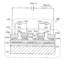
- FIG. 6 is a cross-sectional view showing an example of the configuration of the semiconductor device 20 according to the second embodiment of the present invention.
- the semiconductor device 20 includes a semiconductor element 100 and a control unit 140.
- the same components as those in the first embodiment are denoted by the same reference numerals, and the description thereof is omitted.
- the control unit 140 is a circuit for bringing the semiconductor element 100 into a conductive state. As shown in FIG. 6, the control unit 140 includes current sources 141a, 141b, 142a, and 142b, and switches 143a and 143b.
- the current source 141a is an example of a first current source that generates a first current for applying a voltage equal to or higher than a threshold voltage of a pair of gate electrodes.
- the current source 141a is connected between the first ohmic terminal 106a and the first gate terminal 107a via the switch 143a.
- the current source 141a is configured so that the first potential, which is the potential of the first gate electrode 105a with respect to the first ohmic electrode 104a, is equal to or higher than the threshold voltage of the first gate electrode 105a.
- a gate current IGa1 is supplied to one gate electrode 105a.
- the gate current IGa1 is an example of the first current.
- the current source 142a is an example of a second current source that generates a second current larger than the first current.
- the current source 142a is connected between the first ohmic terminal 106a and the first gate terminal 107a via the switch 143a.
- the current source 142a supplies the gate current IGa2 to the first gate electrode 105a so that the first potential is equal to or higher than the threshold voltage of the first gate electrode 105a.
- the gate current IGa2 is an example of the second current and is larger than the gate current IGa1.
- the switch 143a selects either the current source 141a or the current source 142a according to the polarity of the power supply voltage VSba of the power supply 130. Specifically, the switch 143a is a high-current current source when the power supply voltage VSba of the power supply 130 is positive, that is, when the potential of the second ohmic electrode 104b is higher than the potential of the first ohmic electrode 104a (FIG. 6). 142a is selected. The switch 143a selects the low-current current source 141a when the power supply voltage VSba of the power supply 130 is negative, that is, when the potential of the second ohmic electrode 104b is lower than the potential of the first ohmic electrode 104a.
- the current source 141b is an example of a first current source that generates a first current for applying a voltage equal to or higher than a threshold voltage of a pair of gate electrodes.
- the current source 141b is connected between the second ohmic terminal 106b and the second gate terminal 107b via a switch 143b.
- the current source 141b is configured so that the second potential, which is the potential of the second gate electrode 105b with respect to the second ohmic electrode 104b, is equal to or higher than the threshold voltage of the second gate electrode 105b.
- a gate current IGb1 is supplied to the two-gate electrode 105b.
- the gate current IGb1 is an example of the first current. Further, the gate current IGb1 may be equal to the gate current IGa1.
- the current source 142b is an example of a second current source that generates a second current larger than the first current.
- the current source 142b is connected between the second ohmic terminal 106b and the second gate terminal 107b via the switch 143b.
- the current source 142b supplies the gate current IGb2 to the second gate electrode 105b so that the second potential is equal to or higher than the threshold voltage of the second gate electrode 105b.
- the gate current IGb2 is an example of the second current and is larger than the gate current IGb1. Further, the gate current IGb2 may be equal to the gate current IGa2.
- the switch 143b selects either the current source 141b or the current source 142b according to the polarity of the power supply voltage VSba of the power supply 130. Specifically, the switch 143b is a low-current current source when the power supply voltage VSba of the power supply 130 is positive, that is, when the potential of the second ohmic electrode 104b is higher than the potential of the first ohmic electrode 104a (FIG. 6). 141b is selected. The switch 143b selects the high-current current source 142b when the power supply voltage VSba of the power supply 130 is negative, that is, when the potential of the second ohmic electrode 104b is lower than the potential of the first ohmic electrode 104a.
- the control unit 140 has a potential when the high-potential-side ohmic electrode is used as a reference and is applied to the high-potential-side ohmic electrode.
- the potential of the high-potential side gate electrode corresponding to the low-potential side ohmic electrode is the potential when the potential of the high-potential side gate electrode is based on the low-potential side ohmic electrode,
- the first electric signal is supplied to the high potential side gate electrode and the second electric signal is supplied to the low potential side gate electrode so as to be lower than the first potential.
- the high-potential-side ohmic electrode and the high-potential-side gate electrode are the second ohmic electrode 104b and the second gate electrode 105b.
- the low potential side ohmic electrode and the low potential side gate electrode are the first ohmic electrode 104a and the first gate electrode 105a.
- a gate current IGb1 is supplied as a first electric signal from the low current source 141b to the second gate electrode 105b which is the high potential side gate electrode. Then, the gate current IGa2 is supplied as the second electric signal from the high current source 142a to the first gate electrode 105a which is the low potential side gate electrode. At this time, IGa2> IGb1.
- the high potential side ohmic electrode and the high potential side gate electrode are the first ohmic electrode 104a and the first gate electrode 105a
- the low potential side ohmic electrode and the low potential side gate electrode are the second ohmic electrode.
- the gate electrode 104b and the second gate electrode 105b are used.
- the gate current IGa1 is supplied as the first electric signal from the low current source 141a to the first gate electrode 105a which is the high potential side gate electrode.
- the gate current IGb2 is supplied as the second electric signal from the high current source 142b to the second gate electrode 105b which is the low potential side gate electrode.
- IGb2 > IGa1.
- the control unit 140 of the semiconductor device 20 includes two current sources 141a and 142a between the first ohmic terminal 106a and the first gate terminal 107a.
- the two current sources 141a and 142a respectively generate gate currents IGa1 (first current) and IGa2 (second current) that can apply a potential equal to or higher than the threshold voltage of the first gate electrode 105a.
- the switch 143a selects one of the current sources 141a and 142a. That is, the switch 143a switches the current supplied to the first gate terminal 107a.
- IGa1 is a current for applying a voltage equal to or higher than the threshold voltage of the first gate electrode 105a, and is a current smaller than IGa2.
- the magnitude of IGa2 is set so as to be a gate voltage VGa that allows a saturation current of ISba to flow when VSba> 0.
- control unit 140 includes the current source 141a for low current and the current source 142a for high current, and selects the current to be supplied to the first gate electrode 105a. That is, the control unit 140 can supply IGa1 having a low current or IGa2 having a high current to the first gate electrode 105a by the switch 143a.
- control unit 140 includes two current sources 141b and 142b between the second ohmic terminal 106b and the second gate terminal 107b.
- the two current sources 141b and 142b generate gate currents IGb1 (first current) and IGb2 (second current) that can apply a potential higher than the threshold voltage of the second gate electrode 105b, respectively.
- the switch 143b selects one of the current sources 141b and 142b. That is, the switch 143b switches the current supplied to the second gate terminal 107b.
- IGb1 is a current for applying a voltage equal to or higher than the threshold voltage of the second gate electrode 105b, and is a current smaller than IGb2. Further, the magnitude of IGb2 is set to be a gate voltage VGb that allows a saturation current of ISba to flow when VSba ⁇ 0.
- control unit 140 includes the current source 141b for low current and the current source 142b for high current, and selects the current to be supplied to the second gate electrode 105b. That is, the control unit 140 can supply IGb1 having a low current or IGb2 having a high current to the second gate electrode 105b by the switch 143b.
- IGb1 smaller than IGb2 is supplied to the second gate terminal 107b on the high potential side. Then, the high current IGa2 is supplied to the first gate terminal 107a on the low potential side. Even in this state, a channel is generated in the channel region 103 immediately below the second gate terminal 107b. Accordingly, the driving power of the second gate terminal 107b is reduced.
- IGa1 smaller than IGa2 is supplied to the first gate terminal 107a on the high potential side.
- IGb2 which is a high current, is supplied to the second gate terminal 107b on the low potential side. Even in this state, a channel is generated in the channel region 103 immediately below the second gate terminal 107b. Accordingly, the driving power of the first gate terminal 107a can be suppressed.
- the semiconductor element 100 having the pair of gate electrodes and the pair of ohmic electrodes and the pair of gate electrodes have a voltage equal to or higher than the threshold voltage.
- a control unit 140 is provided that brings the semiconductor element 100 into a conductive state between the pair of ohmic electrodes by supplying a current.
- the control unit 140 supplies a low current to the gate electrode corresponding to the high-potential side ohmic electrode and supplies a high current to the gate electrode corresponding to the low-potential side ohmic electrode when the semiconductor element 100 is conductive. Supply.
- FIG. 7 is a diagram showing an example of the configuration of the semiconductor device 20a according to the variation of the second embodiment of the present invention. Constituent elements similar to those of the second embodiment are denoted by the same reference numerals, and the description thereof is omitted.
- the semiconductor device 20 a includes a control unit 150 instead of the control unit 140.
- the control unit 150 includes current sources 151a and 151b.
- the current source 151a is an example of a current source that generates a current for applying a voltage higher than the threshold voltage of the pair of gate electrodes.
- the current source 151a is connected between the first ohmic terminal 106a and the first gate terminal 107a.
- the current source 151a supplies the gate current IGa as the first electric signal to the first gate terminal 107a.
- the current source 151b is an example of a current source that generates a current for applying a voltage higher than the threshold voltage of the pair of gate electrodes.
- the current source 151b is connected between the second ohmic terminal 106b and the second gate terminal 107b.
- the current source 151b supplies the gate current IGb as the second electric signal to the second gate terminal 107b.
- both IGa and IGb are currents for applying a voltage higher than the threshold voltage of the gate electrode.
- IGa and IGb each have the same current value.
- the decrease of the saturation current of the current ISba flowing from the power source is suppressed and the increase of the gate current is increased. By suppressing the power consumption, power consumption can be reduced.
- the semiconductor device is a semiconductor device including a semiconductor element capable of flowing a current bidirectionally, and the semiconductor element includes a substrate, A semiconductor layer having a channel region formed on the substrate, a pair of ohmic electrodes formed on or above the semiconductor layer and spaced apart from each other, and the pair of ohmics on or above the semiconductor layer And a pair of gate electrodes corresponding to each of the pair of ohmic electrodes formed between the electrodes, and the semiconductor device further includes the semiconductor element and the channel region between the pair of ohmic electrodes.
- a control unit configured to make a conductive state in which a current can flow in both directions through the pair of ohmics when the semiconductor element is in the conductive state.
- the potential when the high potential side ohmic electrode is used as a reference, and the potential of the high potential side gate electrode corresponding to the high potential side ohmic electrode is the same as that of the low potential side ohmic electrode.
- the first electric signal is supplied to the high potential side gate electrode so as to be lower than the potential of the low potential side gate electrode, which is the potential of the reference and is the gate electrode corresponding to the low potential side ohmic electrode.
- a second electric signal is supplied to the low potential side gate electrode.
- the magnitude of the gate current flowing through the high potential side gate electrode depends on the potential difference between the high potential side ohmic electrode and the high potential side gate electrode. Increase is suppressed and power consumption can be reduced.
- the magnitude of the saturation current of the current flowing between the pair of ohmic electrodes depends on the potential difference between the low-potential side ohmic electrode and the low-potential side gate electrode. The magnitude of the current can be maintained. Therefore, power consumption can be reduced while maintaining the characteristics of the power supply current and the power supply voltage.
- control unit includes a first voltage source that generates a first voltage that is equal to or higher than a threshold voltage of the pair of gate electrodes, and a second voltage source that generates a second voltage higher than the first voltage. And the control unit supplies the first voltage as the first electric signal to the high potential side gate electrode, and supplies the second voltage as the second electric signal to the low potential side gate electrode. Also good.
- a high voltage or a low voltage can be easily supplied between each gate electrode and the corresponding ohmic electrode. Accordingly, since the current flowing from the high potential side gate electrode to the channel region can be reduced while maintaining the characteristics of the power supply current and the power supply voltage, the driving power of the high potential side gate electrode can be suppressed.
- the control unit may include a first current source that generates a first current for applying a voltage that is equal to or higher than a threshold voltage of the pair of gate electrodes, and a second current that generates a second current larger than the first current. And the controller supplies the first current to the high potential side gate electrode as the first electrical signal and supplies the second current to the low potential side gate electrode as the second electrical signal. May be.
- the control unit may supply a current for applying a voltage equal to or higher than a threshold voltage of the pair of gate electrodes to the pair of gate electrodes as the first electric signal and the second electric signal.
- the threshold voltage of the pair of gate electrodes may be positive.
- the semiconductor element can be in a cut-off state.
- the semiconductor element may further include a pair of control layers having P-type conductivity formed between the pair of gate electrodes and the semiconductor layer.
- the threshold voltage of the first gate electrode and the threshold voltage of the second gate electrode can be made positive.
- the pair of gate electrodes may be in Schottky junction with the semiconductor layer.
- the threshold voltage of the first gate electrode and the threshold voltage of the second gate electrode can be made positive.
- the semiconductor element may further include an insulating film formed between the pair of gate electrodes and the semiconductor layer.
- the threshold voltage of the first gate electrode and the threshold voltage of the second gate electrode can be made positive.
- the substrate may be a silicon substrate, a sapphire substrate, or a silicon carbide substrate.
- a method for controlling a semiconductor device is a method for controlling a semiconductor device capable of flowing a current in both directions.
- the semiconductor device is formed on a substrate and the substrate, A semiconductor layer having a channel region, a pair of ohmic electrodes formed on or above the semiconductor layer and spaced apart from each other, and formed between the pair of ohmic electrodes on or above the semiconductor layer
- a pair of gate electrodes corresponding to each of the pair of ohmic electrodes, and the method of controlling the semiconductor device is a high potential side which is a gate electrode corresponding to a high potential side ohmic electrode of the pair of ohmic electrodes
- a first electrical signal is supplied to the gate electrode, and a second potential is applied to the low potential side gate electrode that is a gate electrode corresponding to the low potential side ohmic electrode of the pair of ohmic electrodes.
- the potential of the high-potential-side gate electrode when the high-potential-side ohmic electrode is used as a reference is the low-potential-side ohmic
- the first electric signal and the second electric signal are supplied so as to be lower than the potential of the low potential side gate electrode when the electrode is used as a reference.
- the magnitude of the gate current flowing through the high potential side gate electrode depends on the potential difference between the high potential side ohmic electrode and the high potential side gate electrode. Increase is suppressed and power consumption can be reduced.
- the magnitude of the saturation current of the current flowing between the pair of ohmic electrodes depends on the potential difference between the low-potential side ohmic electrode and the low-potential side gate electrode. The magnitude of the current can be maintained. Therefore, power consumption can be reduced while maintaining the characteristics of the power supply current and the power supply voltage.
- the semiconductor device and the control method thereof according to the present invention have been described based on the embodiments, but the present invention is not limited to these embodiments. Unless it deviates from the meaning of this invention, the form which carried out the various deformation
- the control unit 120 applies the high voltage VGa2 generated by the voltage source 122a between the first gate electrode 105a and the first ohmic electrode 104a when the high-potential-side ohmic electrode is the second ohmic electrode 104b.
- the low voltage VGa1 generated by the voltage source 121a may be applied between the second gate electrode 105b and the second ohmic electrode 104b.
- the control unit 120 applies the low voltage VGa1 generated by the voltage source 121a between the first gate electrode 105a and the first ohmic electrode 104a.
- the high voltage VGa2 generated by the voltage source 122a may be applied between the second gate electrode 105b and the second ohmic electrode 104b.
- the control unit 140 supplies the high current IGa2 generated by the current source 142a to the first gate electrode 105a, and generates the low current generated by the current source 141a.
- the current IGa1 may be supplied to the second gate electrode 105b.
- the control unit 140 supplies the low current IGa2 generated by the current source 141a to the first gate electrode 105a, and generates a high current generated by the current source 142a.
- the current IGa1 may be supplied to the second gate electrode 105b.
- the configuration of the semiconductor device is for illustration in order to specifically describe the present invention, and the semiconductor device according to the present invention is not necessarily provided with all of the above configurations. In other words, the semiconductor device according to the present invention need only have a minimum configuration capable of realizing the effects of the present invention.
- the first ohmic terminal 106a, the second ohmic terminal 106b, the first gate terminal 107a, and the second gate terminal 107b may not be provided.
- the semiconductor device and the control method thereof according to the present invention have an effect that an increase in power consumption can be suppressed.
Landscapes
- Junction Field-Effect Transistors (AREA)
- Insulated Gate Type Field-Effect Transistor (AREA)
Abstract
L'invention concerne un dispositif à semi-conducteur (10) qui comprend un élément semiconducteur (100) qui peut commander un courant dans les deux directions. L'élément semiconducteur (100) comprend une paire d'une première électrode ohmique (104a) et d'une seconde électrode ohmique (104b) et une paire d'une première électrode de grille (105a) et d'une seconde électrode de grille (105b). Le dispositif à semi-conducteur (10) comprend également une unité de commande (120) qui met l'élément semiconducteur (100) dans un état électriquement connecté. L'unité de commande (120) fournit un premier signal électrique à une électrode de grille côté potentiel élevé et fournit un second signal électrique à une électrode de grille côté faible potentiel, de sorte que, lorsque l'élément semiconducteur (100) est électriquement connecté, le potentiel de l'électrode de grille côté potentiel élevé, ledit potentiel correspondant à une électrode ohmique côté potentiel élevé, l'électrode ohmique côté potentiel élevé servant de référence, soit inférieur au potentiel de l'électrode de grille côté faible potentiel, ledit potentiel correspondant à l'électrode ohmique côté faible potentiel, l'électrode ohmique côté faible potentiel servant de référence.
Priority Applications (1)
| Application Number | Priority Date | Filing Date | Title |
|---|---|---|---|
| JP2012548654A JP5654044B2 (ja) | 2010-12-14 | 2011-12-13 | 半導体装置及びその制御方法 |
Applications Claiming Priority (2)
| Application Number | Priority Date | Filing Date | Title |
|---|---|---|---|
| JP2010-278636 | 2010-12-14 | ||
| JP2010278636 | 2010-12-14 |
Publications (1)
| Publication Number | Publication Date |
|---|---|
| WO2012081237A1 true WO2012081237A1 (fr) | 2012-06-21 |
Family
ID=46244356
Family Applications (1)
| Application Number | Title | Priority Date | Filing Date |
|---|---|---|---|
| PCT/JP2011/006961 Ceased WO2012081237A1 (fr) | 2010-12-14 | 2011-12-13 | Dispositif à semi-conducteur et son procédé de commande |
Country Status (2)
| Country | Link |
|---|---|
| JP (1) | JP5654044B2 (fr) |
| WO (1) | WO2012081237A1 (fr) |
Cited By (3)
| Publication number | Priority date | Publication date | Assignee | Title |
|---|---|---|---|---|
| JP2017163136A (ja) * | 2016-02-29 | 2017-09-14 | インフィネオン テクノロジーズ オーストリア アクチエンゲゼルシャフト | ダブルゲートトランジスタ素子及び動作方法 |
| CN110890881A (zh) * | 2018-09-10 | 2020-03-17 | 三菱电机株式会社 | 半导体装置 |
| US10903353B2 (en) | 2016-02-29 | 2021-01-26 | Infineon Technologies Austria Ag | Double gate transistor device and method of operating |
Citations (4)
| Publication number | Priority date | Publication date | Assignee | Title |
|---|---|---|---|---|
| JPS5726471A (en) * | 1980-07-24 | 1982-02-12 | Fujitsu Ltd | Semiconductor device |
| WO2008062800A1 (fr) * | 2006-11-20 | 2008-05-29 | Panasonic Corporation | Dispositif à semi-conducteur et son procédé d'entraînement |
| JP2010004588A (ja) * | 2008-06-18 | 2010-01-07 | Panasonic Corp | 双方向スイッチのゲート駆動方法およびそれを用いた電力変換装置 |
| JP2010278333A (ja) * | 2009-05-29 | 2010-12-09 | Furukawa Electric Co Ltd:The | 半導体装置およびその製造方法 |
-
2011
- 2011-12-13 WO PCT/JP2011/006961 patent/WO2012081237A1/fr not_active Ceased
- 2011-12-13 JP JP2012548654A patent/JP5654044B2/ja active Active
Patent Citations (4)
| Publication number | Priority date | Publication date | Assignee | Title |
|---|---|---|---|---|
| JPS5726471A (en) * | 1980-07-24 | 1982-02-12 | Fujitsu Ltd | Semiconductor device |
| WO2008062800A1 (fr) * | 2006-11-20 | 2008-05-29 | Panasonic Corporation | Dispositif à semi-conducteur et son procédé d'entraînement |
| JP2010004588A (ja) * | 2008-06-18 | 2010-01-07 | Panasonic Corp | 双方向スイッチのゲート駆動方法およびそれを用いた電力変換装置 |
| JP2010278333A (ja) * | 2009-05-29 | 2010-12-09 | Furukawa Electric Co Ltd:The | 半導体装置およびその製造方法 |
Cited By (6)
| Publication number | Priority date | Publication date | Assignee | Title |
|---|---|---|---|---|
| JP2017163136A (ja) * | 2016-02-29 | 2017-09-14 | インフィネオン テクノロジーズ オーストリア アクチエンゲゼルシャフト | ダブルゲートトランジスタ素子及び動作方法 |
| US10530360B2 (en) | 2016-02-29 | 2020-01-07 | Infineon Technologies Austria Ag | Double gate transistor device and method of operating |
| US10903353B2 (en) | 2016-02-29 | 2021-01-26 | Infineon Technologies Austria Ag | Double gate transistor device and method of operating |
| US12003231B2 (en) | 2016-02-29 | 2024-06-04 | Infineon Technologies Austria Ag | Double gate transistor device and method of operating |
| CN110890881A (zh) * | 2018-09-10 | 2020-03-17 | 三菱电机株式会社 | 半导体装置 |
| CN110890881B (zh) * | 2018-09-10 | 2023-09-19 | 三菱电机株式会社 | 半导体装置 |
Also Published As
| Publication number | Publication date |
|---|---|
| JP5654044B2 (ja) | 2015-01-14 |
| JPWO2012081237A1 (ja) | 2014-05-22 |
Similar Documents
| Publication | Publication Date | Title |
|---|---|---|
| CN105247681B (zh) | 增强型iii-氮化物器件 | |
| JP6201422B2 (ja) | 半導体装置 | |
| JP5575816B2 (ja) | 複合型半導体装置 | |
| JP5653326B2 (ja) | 窒化物半導体装置 | |
| CN106024878B (zh) | 具有集成到栅极结构中的rc网络的高电子迁移率晶体管 | |
| CN102315272B (zh) | 双向开关、交流二线式开关、开关电源电路以及双向开关的驱动方法 | |
| US20080143421A1 (en) | Bidirectional switch and method for driving bidirectional switch | |
| US20090072269A1 (en) | Gallium nitride diodes and integrated components | |
| JP2009159222A (ja) | スイッチ装置 | |
| JP2010539712A (ja) | Iii族窒化物双方向スイッチ | |
| JP2012212875A (ja) | 低電圧デバイス保護付き高電圧複合半導体デバイス | |
| CN112585751B (zh) | 电阻元件及功率放大电路 | |
| US9165922B2 (en) | Semiconductor device | |
| US9196686B2 (en) | Diode circuit and DC to DC converter | |
| JP5654044B2 (ja) | 半導体装置及びその制御方法 | |
| JP6701767B2 (ja) | 半導体装置 | |
| WO2022172625A1 (fr) | Dispositif à semi-conducteur | |
| CN107667422A (zh) | 复合型半导体装置 | |
| CN110383435A (zh) | 半导体装置 | |
| US12439661B2 (en) | Semiconductor device | |
| JP5853187B2 (ja) | スイッチ装置 | |
| CN105070752B (zh) | 一种具有集成二极管的异质结器件 | |
| JP2008172035A (ja) | ショットキーダイオード | |
| WO2021039631A1 (fr) | Dispositif à semi-conducteur | |
| US10128326B2 (en) | Resistor having increasing resistance due to increasing voltage |
Legal Events
| Date | Code | Title | Description |
|---|---|---|---|
| 121 | Ep: the epo has been informed by wipo that ep was designated in this application |
Ref document number: 11848336 Country of ref document: EP Kind code of ref document: A1 |
|
| ENP | Entry into the national phase |
Ref document number: 2012548654 Country of ref document: JP Kind code of ref document: A |
|
| NENP | Non-entry into the national phase |
Ref country code: DE |
|
| 122 | Ep: pct application non-entry in european phase |
Ref document number: 11848336 Country of ref document: EP Kind code of ref document: A1 |