WO2012102011A1 - Dispositif à semi-conducteur à base de nitrure de gallium et procédé de production du dispositif à semi-conducteur - Google Patents
Dispositif à semi-conducteur à base de nitrure de gallium et procédé de production du dispositif à semi-conducteur Download PDFInfo
- Publication number
- WO2012102011A1 WO2012102011A1 PCT/JP2012/000404 JP2012000404W WO2012102011A1 WO 2012102011 A1 WO2012102011 A1 WO 2012102011A1 JP 2012000404 W JP2012000404 W JP 2012000404W WO 2012102011 A1 WO2012102011 A1 WO 2012102011A1
- Authority
- WO
- WIPO (PCT)
- Prior art keywords
- layer
- semiconductor device
- semiconductor layer
- semiconductor
- recess
- Prior art date
- Legal status (The legal status is an assumption and is not a legal conclusion. Google has not performed a legal analysis and makes no representation as to the accuracy of the status listed.)
- Ceased
Links
Images











Classifications
-
- H—ELECTRICITY
- H10—SEMICONDUCTOR DEVICES; ELECTRIC SOLID-STATE DEVICES NOT OTHERWISE PROVIDED FOR
- H10P—GENERIC PROCESSES OR APPARATUS FOR THE MANUFACTURE OR TREATMENT OF DEVICES COVERED BY CLASS H10
- H10P50/00—Etching of wafers, substrates or parts of devices
- H10P50/60—Wet etching
- H10P50/64—Wet etching of semiconductor materials
- H10P50/642—Chemical etching
-
- H—ELECTRICITY
- H10—SEMICONDUCTOR DEVICES; ELECTRIC SOLID-STATE DEVICES NOT OTHERWISE PROVIDED FOR
- H10D—INORGANIC ELECTRIC SEMICONDUCTOR DEVICES
- H10D30/00—Field-effect transistors [FET]
- H10D30/01—Manufacture or treatment
- H10D30/015—Manufacture or treatment of FETs having heterojunction interface channels or heterojunction gate electrodes, e.g. HEMT
-
- H—ELECTRICITY
- H10—SEMICONDUCTOR DEVICES; ELECTRIC SOLID-STATE DEVICES NOT OTHERWISE PROVIDED FOR
- H10D—INORGANIC ELECTRIC SEMICONDUCTOR DEVICES
- H10D30/00—Field-effect transistors [FET]
- H10D30/01—Manufacture or treatment
- H10D30/021—Manufacture or treatment of FETs having insulated gates [IGFET]
-
- H—ELECTRICITY
- H10—SEMICONDUCTOR DEVICES; ELECTRIC SOLID-STATE DEVICES NOT OTHERWISE PROVIDED FOR
- H10D—INORGANIC ELECTRIC SEMICONDUCTOR DEVICES
- H10D30/00—Field-effect transistors [FET]
- H10D30/40—FETs having zero-dimensional [0D], one-dimensional [1D] or two-dimensional [2D] charge carrier gas channels
- H10D30/47—FETs having zero-dimensional [0D], one-dimensional [1D] or two-dimensional [2D] charge carrier gas channels having two-dimensional [2D] charge carrier gas channels, e.g. nanoribbon FETs or high electron mobility transistors [HEMT]
- H10D30/471—High electron mobility transistors [HEMT] or high hole mobility transistors [HHMT]
- H10D30/473—High electron mobility transistors [HEMT] or high hole mobility transistors [HHMT] having confinement of carriers by multiple heterojunctions, e.g. quantum well HEMT
- H10D30/4732—High electron mobility transistors [HEMT] or high hole mobility transistors [HHMT] having confinement of carriers by multiple heterojunctions, e.g. quantum well HEMT using Group III-V semiconductor material
-
- H—ELECTRICITY
- H10—SEMICONDUCTOR DEVICES; ELECTRIC SOLID-STATE DEVICES NOT OTHERWISE PROVIDED FOR
- H10D—INORGANIC ELECTRIC SEMICONDUCTOR DEVICES
- H10D30/00—Field-effect transistors [FET]
- H10D30/60—Insulated-gate field-effect transistors [IGFET]
- H10D30/63—Vertical IGFETs
-
- H—ELECTRICITY
- H10—SEMICONDUCTOR DEVICES; ELECTRIC SOLID-STATE DEVICES NOT OTHERWISE PROVIDED FOR
- H10P—GENERIC PROCESSES OR APPARATUS FOR THE MANUFACTURE OR TREATMENT OF DEVICES COVERED BY CLASS H10
- H10P14/00—Formation of materials, e.g. in the shape of layers or pillars
- H10P14/20—Formation of materials, e.g. in the shape of layers or pillars of semiconductor materials
- H10P14/34—Deposited materials, e.g. layers
- H10P14/3402—Deposited materials, e.g. layers characterised by the chemical composition
-
- H—ELECTRICITY
- H10—SEMICONDUCTOR DEVICES; ELECTRIC SOLID-STATE DEVICES NOT OTHERWISE PROVIDED FOR
- H10P—GENERIC PROCESSES OR APPARATUS FOR THE MANUFACTURE OR TREATMENT OF DEVICES COVERED BY CLASS H10
- H10P50/00—Etching of wafers, substrates or parts of devices
-
- H—ELECTRICITY
- H10—SEMICONDUCTOR DEVICES; ELECTRIC SOLID-STATE DEVICES NOT OTHERWISE PROVIDED FOR
- H10P—GENERIC PROCESSES OR APPARATUS FOR THE MANUFACTURE OR TREATMENT OF DEVICES COVERED BY CLASS H10
- H10P50/00—Etching of wafers, substrates or parts of devices
- H10P50/20—Dry etching; Plasma etching; Reactive-ion etching
- H10P50/24—Dry etching; Plasma etching; Reactive-ion etching of semiconductor materials
- H10P50/246—Dry etching; Plasma etching; Reactive-ion etching of semiconductor materials of Group III-V materials
-
- H—ELECTRICITY
- H10—SEMICONDUCTOR DEVICES; ELECTRIC SOLID-STATE DEVICES NOT OTHERWISE PROVIDED FOR
- H10P—GENERIC PROCESSES OR APPARATUS FOR THE MANUFACTURE OR TREATMENT OF DEVICES COVERED BY CLASS H10
- H10P70/00—Cleaning of wafers, substrates or parts of devices
- H10P70/20—Cleaning during device manufacture
-
- H—ELECTRICITY
- H10—SEMICONDUCTOR DEVICES; ELECTRIC SOLID-STATE DEVICES NOT OTHERWISE PROVIDED FOR
- H10D—INORGANIC ELECTRIC SEMICONDUCTOR DEVICES
- H10D62/00—Semiconductor bodies, or regions thereof, of devices having potential barriers
- H10D62/80—Semiconductor bodies, or regions thereof, of devices having potential barriers characterised by the materials
- H10D62/85—Semiconductor bodies, or regions thereof, of devices having potential barriers characterised by the materials being Group III-V materials, e.g. GaAs
- H10D62/8503—Nitride Group III-V materials, e.g. AlN or GaN
-
- H—ELECTRICITY
- H10—SEMICONDUCTOR DEVICES; ELECTRIC SOLID-STATE DEVICES NOT OTHERWISE PROVIDED FOR
- H10D—INORGANIC ELECTRIC SEMICONDUCTOR DEVICES
- H10D64/00—Electrodes of devices having potential barriers
- H10D64/20—Electrodes characterised by their shapes, relative sizes or dispositions
- H10D64/27—Electrodes not carrying the current to be rectified, amplified, oscillated or switched, e.g. gates
- H10D64/311—Gate electrodes for field-effect devices
- H10D64/411—Gate electrodes for field-effect devices for FETs
- H10D64/511—Gate electrodes for field-effect devices for FETs for IGFETs
- H10D64/512—Disposition of the gate electrodes, e.g. buried gates
- H10D64/513—Disposition of the gate electrodes, e.g. buried gates within recesses in the substrate, e.g. trench gates, groove gates or buried gates
-
- H—ELECTRICITY
- H10—SEMICONDUCTOR DEVICES; ELECTRIC SOLID-STATE DEVICES NOT OTHERWISE PROVIDED FOR
- H10D—INORGANIC ELECTRIC SEMICONDUCTOR DEVICES
- H10D64/00—Electrodes of devices having potential barriers
- H10D64/60—Electrodes characterised by their materials
- H10D64/66—Electrodes having a conductor capacitively coupled to a semiconductor by an insulator, e.g. MIS electrodes
- H10D64/68—Electrodes having a conductor capacitively coupled to a semiconductor by an insulator, e.g. MIS electrodes characterised by the insulator, e.g. by the gate insulator
-
- H—ELECTRICITY
- H10—SEMICONDUCTOR DEVICES; ELECTRIC SOLID-STATE DEVICES NOT OTHERWISE PROVIDED FOR
- H10P—GENERIC PROCESSES OR APPARATUS FOR THE MANUFACTURE OR TREATMENT OF DEVICES COVERED BY CLASS H10
- H10P14/00—Formation of materials, e.g. in the shape of layers or pillars
- H10P14/20—Formation of materials, e.g. in the shape of layers or pillars of semiconductor materials
- H10P14/29—Formation of materials, e.g. in the shape of layers or pillars of semiconductor materials characterised by the substrates
- H10P14/2901—Materials
-
- H—ELECTRICITY
- H10—SEMICONDUCTOR DEVICES; ELECTRIC SOLID-STATE DEVICES NOT OTHERWISE PROVIDED FOR
- H10P—GENERIC PROCESSES OR APPARATUS FOR THE MANUFACTURE OR TREATMENT OF DEVICES COVERED BY CLASS H10
- H10P14/00—Formation of materials, e.g. in the shape of layers or pillars
- H10P14/20—Formation of materials, e.g. in the shape of layers or pillars of semiconductor materials
- H10P14/32—Formation of materials, e.g. in the shape of layers or pillars of semiconductor materials characterised by intermediate layers between substrates and deposited layers
- H10P14/3202—Materials thereof
- H10P14/3214—Materials thereof being Group IIIA-VA semiconductors
- H10P14/3216—Nitrides
-
- H—ELECTRICITY
- H10—SEMICONDUCTOR DEVICES; ELECTRIC SOLID-STATE DEVICES NOT OTHERWISE PROVIDED FOR
- H10P—GENERIC PROCESSES OR APPARATUS FOR THE MANUFACTURE OR TREATMENT OF DEVICES COVERED BY CLASS H10
- H10P14/00—Formation of materials, e.g. in the shape of layers or pillars
- H10P14/20—Formation of materials, e.g. in the shape of layers or pillars of semiconductor materials
- H10P14/32—Formation of materials, e.g. in the shape of layers or pillars of semiconductor materials characterised by intermediate layers between substrates and deposited layers
- H10P14/3242—Structure
- H10P14/3244—Layer structure
- H10P14/3251—Layer structure consisting of three or more layers
- H10P14/3252—Alternating layers, e.g. superlattice
-
- H—ELECTRICITY
- H10—SEMICONDUCTOR DEVICES; ELECTRIC SOLID-STATE DEVICES NOT OTHERWISE PROVIDED FOR
- H10P—GENERIC PROCESSES OR APPARATUS FOR THE MANUFACTURE OR TREATMENT OF DEVICES COVERED BY CLASS H10
- H10P14/00—Formation of materials, e.g. in the shape of layers or pillars
- H10P14/20—Formation of materials, e.g. in the shape of layers or pillars of semiconductor materials
- H10P14/34—Deposited materials, e.g. layers
- H10P14/3402—Deposited materials, e.g. layers characterised by the chemical composition
- H10P14/3414—Deposited materials, e.g. layers characterised by the chemical composition being group IIIA-VIA materials
- H10P14/3416—Nitrides
-
- H—ELECTRICITY
- H10—SEMICONDUCTOR DEVICES; ELECTRIC SOLID-STATE DEVICES NOT OTHERWISE PROVIDED FOR
- H10P—GENERIC PROCESSES OR APPARATUS FOR THE MANUFACTURE OR TREATMENT OF DEVICES COVERED BY CLASS H10
- H10P14/00—Formation of materials, e.g. in the shape of layers or pillars
- H10P14/20—Formation of materials, e.g. in the shape of layers or pillars of semiconductor materials
- H10P14/38—Formation of materials, e.g. in the shape of layers or pillars of semiconductor materials characterised by treatments done after the formation of the materials
Definitions
- the present invention relates to a gallium nitride (GaN) semiconductor device and a method for manufacturing the semiconductor device.
- GaN gallium nitride
- Non-Patent Document 1 IEICE Technical Report, IEICE, 2009, ED2009-43
- inductively coupled plasma has a high electron temperature.
- ICP-RIE a high-energy ion species collides with the surface of the semiconductor, and the etched surface is not flat but uneven, and the semiconductor device is damaged to deteriorate the electrical characteristics of the semiconductor device.
- a chlorine-based gas such as chlorine (Cl 2 ) or boron trichloride (BCl 3 ) is used as an etching gas, chloride or the like is formed on the surface, and the etched surface Chlorine remains. Residual chlorine, as an impurity, deteriorates electrical characteristics by inhibiting carrier flow in the GaN-based semiconductor device.
- an object of one aspect of the present invention is to provide a gallium nitride semiconductor device and a method for manufacturing the semiconductor device that can solve the above-described problems. This object is achieved by a combination of features described in the independent claims.
- the dependent claims define further advantageous specific examples of the present invention.
- the first sacrificial layer is in contact with at least a part of the first semiconductor layer and has a higher solid solubility of impurities contained in the first semiconductor layer than the first semiconductor layer.
- An electrode forming step of forming an electrode layer is provided.
- a first semiconductor layer a recess from which a part of the first semiconductor layer has been removed, and a first GaN-based semiconductor formed under the first semiconductor layer.
- a GaN-based semiconductor device including two semiconductor layers, wherein the halogen present in the recess surface of the second semiconductor layer in the recess portion is 3 atom% or less.
- a method for manufacturing a semiconductor device for manufacturing a GaN-based semiconductor device including a recess portion forming step of performing dry etching by a plasma process to form a recess portion.
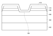
- FIG. 1 is a cross-sectional view of a semiconductor device according to the present invention.
- the manufacturing method which concerns on 1st Embodiment of the semiconductor device which concerns on 1st Embodiment shown in FIG. 1 is shown.
- the manufacturing method which concerns on 1st Embodiment of the semiconductor device which concerns on 1st Embodiment shown in FIG. 1 is shown.
- the manufacturing method which concerns on 1st Embodiment of the semiconductor device which concerns on 1st Embodiment shown in FIG. 1 is shown.
- It is sectional drawing of a microwave plasma apparatus.
- a manufacturing method according to a second embodiment of the semiconductor device according to the first embodiment shown in FIG. 1 will be described.
- a manufacturing method according to a second embodiment of the semiconductor device according to the first embodiment shown in FIG. 1 will be described.
- a manufacturing method according to a second embodiment of the semiconductor device according to the first embodiment shown in FIG. 1 will be described.
- a manufacturing method according to a second embodiment of the semiconductor device according to the first embodiment shown in FIG. 1 will be described.
- a manufacturing method according to a second embodiment of the semiconductor device according to the first embodiment shown in FIG. 1 will be described.
- It is an AFM image of the surface of the semiconductor device manufactured with the manufacturing method concerning a 2nd embodiment. 6 shows CV characteristics of a semiconductor device manufactured by the manufacturing method according to the first and second embodiments.
- the JE characteristic of the semiconductor device manufactured by the manufacturing method according to the first and second embodiments is shown.
- the transfer characteristic of the semiconductor device manufactured with the manufacturing method concerning the 1st and 2nd embodiment is shown.
- the field effect mobility of a carrier of the semiconductor device manufactured with the manufacturing method concerning the 1st and 2nd embodiments is shown.
- the SIMS measurement result of the semiconductor substrate shown in FIG. 13 is shown.
- the SIMS measurement result of the semiconductor substrate shown in FIG. 14 is shown.
- FIG. 1 is a schematic cross-sectional view of a semiconductor device 100 manufactured by a manufacturing method according to the first or second embodiment of the present invention.
- the semiconductor device 100 is, for example, a GaN-based MOS field effect transistor.
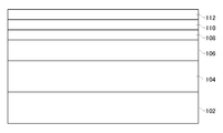
- the semiconductor device 100 includes a substrate 102, a buffer layer 104, a channel layer 106, a drift layer 108, an electron supply layer 110, a gate insulating film 120, a source electrode 122, a drain electrode 124, and a gate electrode 126.
- the substrate 102 may be a silicon substrate having a (111) plane as a main surface.
- the substrate 102 may be a sapphire substrate having a (0001) c-plane as a main surface. Further, the substrate 102 may be a SiC substrate or a GaN substrate.
- the buffer layer 104 is formed on the substrate 102.
- the buffer layer 104 is a semiconductor layer in which, for example, a semiconductor layer made of GaN and a semiconductor layer made of AlN are alternately stacked by 8 layers each.
- the thickness of the semiconductor layer made of GaN is, for example, 200 nm.
- the thickness of the semiconductor layer made of AlN is, for example, 20 nm.
- the channel layer 106 is formed on the buffer layer 104.
- the channel layer 106 is, for example, a semiconductor layer made of p-type GaN having a thickness of 500 nm doped with Mg to about 1 ⁇ 10 17 cm ⁇ 3 .
- the dopant in the channel layer 106 may be Zn or Be.
- the drift layer 108 is formed on the channel layer 106.
- the drift layer 108 is a semiconductor layer (u-GaN layer) made of undoped GaN having a thickness of 20 nm, for example.
- As the drift layer 108 a semiconductor layer made of GaN having a p-type impurity concentration lower than that of the channel layer 106 may be used.
- the electron supply layer 110 is formed on the drift layer 108.
- the Al composition ratio in the electron supply layer 110 may be set in a range of 0 ⁇ Y ⁇ 1.
- Al Y Ga 1-Y N has a larger band gap than GaN. Due to the difference in the band gap and the piezoelectric effect, a two-dimensional electron gas is formed in the vicinity of the interface between the drift layer 108 and the electron supply layer 110.
- a recess 116 is formed in a part between the source electrode 122 and the drain electrode 124.
- the electron supply layer 110 and a part of the drift layer 108 are removed.
- a part of the surface of the channel layer 106 formed under the electron supply layer 110 and the drift layer 108 is removed to form a recess surface 128.
- the gate insulating film 120 is formed in contact with and covering the recess surface 128 of the channel layer 106, the side surface of the drift layer 108, and the side surface and the surface of the electron supply layer 110.
- the gate insulating film 120 is a SiO 2 film having a thickness of 60 nm, for example. However, the gate insulating film 120 is removed in a portion where the source electrode 122 and the drain electrode 124 are formed.
- the source electrode 122 and the drain electrode 124 are formed on a part of the electron supply layer 110.
- Each of the source electrode 122 and the drain electrode 124 is a composite layer in which, for example, an Al layer having a thickness of 300 nm is formed on a Ti layer having a thickness of 25 nm.
- the source electrode 122 and the drain electrode 124 may be formed over the entire electron supply layer 110.
- the source electrode 122 and the drain electrode 124 may be other metal materials having a high work function, and may be, for example, a composite layer made of Ti / AlSi / Mo.
- the gate electrode 126 is formed on the gate insulating film 120 in the recess portion 116.
- the gate electrode 126 is, for example, a composite layer in which an Al layer having a thickness of 300 nm is formed on a Ti layer having a thickness of 25 nm.
- the gate electrode 126 may be a composite layer made of Ti / Au.
- the electron supply layer 110 and the drift layer 108 are removed at the end of the semiconductor device 100 and insulated from other adjacent elements. Further, all or part of the channel layer 106 and the buffer layer 104 may be removed at the end portion of the semiconductor device 100 to improve insulation from other adjacent elements.
- FIG. 2A to 2C show a method of manufacturing the semiconductor device 100 shown in FIG. 1 according to the first embodiment of the present invention.
- the elements denoted by the same reference numerals as those in FIG. 1 may have the same functions and configurations as the elements described in FIG.
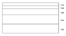
- FIG. 2A shows a state where the buffer layer 104, the channel layer 106, the drift layer 108, and the electron supply layer 110 are formed on the substrate 102.
- a buffer layer 104 in which a plurality of GaN layers and AlN layers are stacked on a substrate 102 and a channel layer 106 made of p-type GaN are formed using trimethylgallium (TMGa), trimethylaluminum (TMAl), and ammonia (NH 3 ). Then, it may be epitaxially grown by the MOCVD method.
- Bis (cyclopentadienyl) magnesium (Cp 2 Mg) may be used as a Mg doping source of the channel layer 106.
- a drift layer 108 made of u-GaN may be epitaxially grown on the channel layer 106 by MOCVD using TMGa and NH 3 . Further, an electron supply layer made of Al Y Ga 1-Y N may be epitaxially grown on the drift layer 108 by MOCVD using TMGa, TMAl, and NH 3 .
- the growth temperature of the buffer layer 104, the channel layer 106, the drift layer 108, and the electron supply layer 110 may be 1050 ° C., and hydrogen gas may be used as a carrier gas.
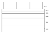
- FIG. 2B shows a state in which a mask layer 114 is formed on the electron supply layer 110 shown in FIG. 2A.
- the mask layer 114 is made of amorphous silicon, for example.
- An amorphous silicon (a-Si) layer having a thickness of 500 nm is formed on the electron supply layer 110 by plasma enhanced chemical vapor deposition (PCVD).
- PCVD plasma enhanced chemical vapor deposition
- the formed a-Si layer is patterned by photolithography and dry etching using CF 4 gas to form a mask layer 114.
- FIG. 2C shows a state in which the recess 116 is formed.
- the recess 116 is formed by dry etching using a bromine-based gas by a microwave plasma process.
- the microwave plasma process is a process of etching an object with an etching gas that has been turned into plasma by microwaves.
- Portions of the electron supply layer 110 and the drift layer 108 that are not covered with the mask layer 114 are dry-etched to penetrate in the depth direction, and the channel layer 106 that is formed under the drift layer 108 includes the portions.
- the recess surface 128 may be formed by being partially exposed. Further, a recess surface 128 of the channel layer 106 may be formed by dry etching a part of the surface of the channel layer 106.
- the bromine-based etching gas is, for example, hydrogen bromide (HBr).
- the bromine-based etching gas may be bromine (Br 2 ), boron tribromide (BBr 3 ), or a mixed gas thereof.
- the gate insulating film 120 made of SiO 2 may be formed by PCVD using SiH 4 and N 2 O as source gases. A part of the gate insulating film 120 may be removed with hydrofluoric acid to expose the electron supply layer 110.
- the source electrode 122 and the drain electrode 124 may be formed on the exposed portion of the electron supply layer 110 by a lift-off method.
- the gate electrode 126 may be formed on the gate insulating film 120 of the recess portion 116 by a lift-off method.
- FIG. 3 is a schematic cross-sectional view of a microwave plasma apparatus 250 that performs dry etching by a microwave plasma process.
- the microwave plasma apparatus 250 includes a stage 254, an antenna 262 that supplies a microwave, a dielectric 256 that introduces a microwave, a shower head 260 that introduces an etching gas between the dielectric and the processing substrate, and plasma.
- a processing chamber 258 for performing the processing used is provided.
- a processing substrate 252 is disposed on the stage 254.
- the bromine-based gas introduced from the shower head 260 is turned into plasma by the microwave introduced from the dielectric 256, and the semiconductor layer formed on the processing substrate 252 is dry-etched.
- the antenna 262 is, for example, a planar antenna having a plurality of slot-shaped holes.
- the antenna 262 may be an RLSA (radian line slot antenna).
- a microwave having a frequency of 915 MHz is used.
- a microwave having a frequency between 900 MHz and 2.5 GHz can be used.
- a microwave of 1.98 GHz or 2.45 GHz can be used.
- FIG. 4 is an AFM photograph of the recess surface 128 of the channel layer 106 formed by the process shown in FIG. 2C. Since the microwave plasma process is excellent in uniformity, the arithmetic average roughness Ra of the recess surface 128 of the channel layer 106 is 1 nm or less, and the difference PV between the maximum peak height and the maximum valley depth of the cross section curve of the recess surface 128 is 15 nm. The root mean square roughness RMS of the recess surface 128 is 1.4 nm or less.
- the arithmetic average roughness Ra of the recess surface 128 is 0.6773 nm, and the difference PV between the maximum peak height and the maximum valley depth of the sectional curve is 11.61 nm.
- the root mean square RMS was 1.235 nm.
- FIG. 5 shows, as a comparative example, when the etching of a part of the electron supply layer 110 and the drift layer 108 and the etching of a part of the surface of the channel layer 106 are performed by ICP-RIE to obtain the state of FIG. It is an AFM photograph of the recess surface 128.
- the arithmetic mean roughness Ra of the recess surface 128 was 1.1112 nm
- the difference PV between the maximum peak height and the maximum valley depth of the sectional curve was 16.27 nm
- the root mean square roughness RMS was 1.436 nm.
- Dielectrically coupled plasma has a high electron temperature, and high energy ion species collide with the recess surface 128, so that the unevenness of the etched surface becomes large.
- Table 1 shows the results of analyzing the elemental composition of the recess surface 128 shown in FIG. 4 by X-ray photoelectron spectroscopy (XPS).
- XPS X-ray photoelectron spectroscopy
- part of the electron supply layer 110 and the drift layer 108 and part of the surface of the channel layer 106 are dry-etched by a microwave plasma process using chlorine gas (Cl 2 ) to obtain the state of FIG. 2C.
- the surface composition of the recess surface 128 is shown.
- the element described as 0.0 atom% was below the lower limit of detection by XPS analysis.
- the halogen present on the recess surface 128 of the channel layer is 3 atom% or less.
- HBr is used as an etching gas
- the halogen present in the recess surface 128 is 0.2 atom%.
- a chlorine-based gas is used as an etching gas
- a large amount of halogen remains on the surface of the GaN-based semiconductor after the etching.
- 4.6 atom% of chlorine remained on the recess surface 128. This is because chlorine tends to remain on the semiconductor surface. If halogen atoms remain on the surface of the channel layer 106, the field-effect mobility of carriers decreases. Therefore, it is preferable to reduce halogen remaining on the surface of the channel layer 106.
- FIG. 6A to 6E show a method for manufacturing the semiconductor device 100 of FIG. 1 according to the second embodiment of the present invention.
- the same reference numerals as those in FIG. 1 or 2A to 2C may have the same functions and configurations as the elements described in FIG. 1 or 2A to 2C.
- FIG. 6A shows a state in which the buffer layer 104, the channel layer 106, the drift layer 108, and the electron supply layer 110 are formed on the substrate 102.
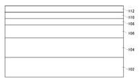
- FIG. 6B shows a state in which the first sacrificial layer 112 is formed in contact with the electron supply layer 110 shown in FIG. 6A.
- the first sacrificial layer 112 has a higher solid solubility of impurities contained in the electron supply layer 110, which is a semiconductor layer formed in contact with the first sacrificial layer 112, than the electron supply layer 110.
- the impurities in the semiconductor layer include an oxide formed by oxidizing the surface of the semiconductor layer and other impurities present on the surface of the semiconductor layer.
- the electron supply layer 110 may be formed of Al Y Ga 1-Y N. Nitrogen having a high vapor pressure is selectively released from the surface of the electron supply layer 110 made of Al Y Ga 1-Y N, and Al and Ga are present in an amount larger than the stoichiometric amount and become impurities. Further, gallium oxide, aluminum oxide, or the like is present as an impurity on the surface of the electron supply layer 110 made of Al Y Ga 1-Y N.
- SiO 2 has a higher solid solubility of the impurities than Al Y Ga 1-Y N. Accordingly, the first sacrificial layer 112 may be made of SiO 2.
- the first sacrificial layer 112 may be in contact with the entire surface of the electron supply layer 110. Alternatively, the first sacrificial layer 112 may be formed in contact with a part of the electron supply layer 110 in order to process a part of the electron supply layer 110.
- the first sacrificial layer 112 made of SiO 2 is formed by PCVD using SiH 4 and N 2 O as source gases.
- the film thickness of the first sacrificial layer 112 is, for example, 60 nm.
- the first sacrificial layer 112 and the electron supply layer 110 may be annealed.
- the annealing temperature may be 600 ° C. or higher.
- the first sacrificial layer 112 and the electron supply layer 110 are annealed at 800 ° C. for 30 minutes in a nitrogen atmosphere.
- An electric furnace may be used for annealing. Since the impurity solubility of the electron supply layer 110 is higher than that of the electron supply layer 110 with respect to the first sacrificial layer 112, the impurities diffuse from the electron supply layer 110 to the first sacrificial layer 112 during annealing. To do.
- gallium and gallium oxide on the surface of the electron supply layer 110 which are impurities of the electron supply layer 110 made of Al Y Ga 1-Y N, diffuse into the first sacrificial layer 112.
- the first sacrificial layer 112 is removed by a wet process.
- an etchant that can selectively wet-etch the first sacrificial layer 112 with respect to the electron supply layer 110 is used.
- An etchant of hydrofluoric acid that can selectively etch SiO 2 can be used.
- buffered hydrofluoric acid controlled at a liquid temperature of 23 ° C. is used.
- the impurities in the electron supply layer 110 diffused into the first sacrificial layer 112 are removed together with the first sacrificial layer 112 by wet etching. Thereby, a clean and flat surface of the electron supply layer 110 is obtained.
- the step of forming the first sacrificial layer 112, the step of annealing the first sacrificial layer 112 and the electron supply layer 110, and the step of removing the first sacrificial layer 112 may be repeated two or more times. Good. Thereby, the surface of the electron supply layer 110 can be further cleaned.
- FIG. 6C shows a state in which the mask layer 114 is formed on the electron supply layer 110 shown in FIG. 6B.
- the mask layer 114 may be formed of a-Si.
- the mask layer 114 may be formed by the same method as the mask layer 114 shown in FIG. 2B.
- FIG. 6D shows a state in which the recess 116 is formed.
- the recess 116 in this example may be formed by the same method as the recess 116 in FIG. 2C.
- a part of the channel layer 106 may be exposed to form a recess surface 128. Since the impurities on the surface of the electron supply layer 110 are removed before dry-etching a part of the electron supply layer 110 and the drift layer 108, a flat recess surface 128 can be formed.
- FIG. 6E shows a state in which the second sacrificial layer 118 is formed.
- the second sacrificial layer 118 is formed in contact with the exposed recess surface 128 of the channel layer 106.
- the second sacrificial layer 118 has a higher solid solubility of impurities contained in the channel layer 106, which is a semiconductor layer formed in contact with the second sacrificial layer 118, than the channel layer 106.
- the channel layer 106 may be formed of p-type GaN.
- nitrogen having a high vapor pressure is selectively separated, and Ga is present in an amount larger than the stoichiometric amount, which is an impurity.
- gallium oxide or the like is present as an impurity on the surface of the channel layer 106 made of p-type GaN.
- the impurity in the channel layer here does not include a p-type GaN dopant.
- SiO 2 has a higher solid solubility of the impurities than p-type GaN.
- the second sacrificial layer 118 may consist of SiO 2.
- the second sacrificial layer 118 is in contact with the recess surface 128 where the channel layer 106 is exposed.
- the second sacrificial layer 118 may also cover the patterned drift layer 108 and the electron supply layer 110.
- the second sacrificial layer 118 made of SiO 2 is formed by PCVD using SiH 4 and N 2 O as source gases.
- the film thickness of the second sacrificial layer 118 is, for example, 60 nm.
- annealing of the second sacrificial layer 118 and the channel layer 106 and removal of the second sacrificial layer 118 are performed in the same manner as the first sacrificial layer 112. Impurities on the recess surface 128 of the channel layer 106 are diffused into the second sacrificial layer 118 by the annealing of the second sacrificial layer 118 and the channel layer.
- the annealing Ga, Ga oxide, and the like, which are impurities in the channel layer 106, diffuse into the second sacrificial layer 118.
- the impurities are removed together with the second sacrificial layer 118 when the second sacrificial layer 118 is removed by a wet process, and a clean and flat recess surface 128 of the channel layer 106 is obtained.
- the gate insulating film 120 may be formed in contact with and covering the recess surface 128 of the channel layer 106, the side surface of the drift layer 108, and the side surface and surface of the electron supply layer 110.
- the gate insulating film 120 is removed from a part of the surface of the electron supply layer 110, the source electrode 122 and the drain electrode 124 are formed in the portion where the gate insulating film 120 is removed, and the semiconductor device 100 of FIG. 1 is manufactured. Good.
- the step of forming the second sacrificial layer 118, the step of annealing the second sacrificial layer 118 and the channel layer 106, and the step of removing the second sacrificial layer 118 may be repeated twice or more.
- the manufacturing method other than the above is the same as the manufacturing method according to the first embodiment.
- the semiconductor device 100 of FIG. 1 is obtained.
- the first sacrificial layer 112 and the second sacrificial layer 118 are preferably formed at a temperature of the substrate 102 of 500 ° C. or lower.
- nitrogen (N) is detached from the GaN-based semiconductor, and the composition may deviate from the stoichiometry.
- the first sacrificial layer 112 and the second sacrificial layer 118 are not limited to SiO 2 formed by CVD, and are formed by CVD, sputtering, or vapor deposition, SiO X (0 ⁇ X ⁇ 2), AlO X.
- It may be a film made of at least one of TiO X (0 ⁇ X ⁇ 2), NiO X (0 ⁇ X ⁇ 1.5), and vanadium (V). This is because the solid solubility of impurities in GaN-based semiconductors is higher for these materials than GaN-based impurities.
- the sacrificial layer 112 or the second sacrificial layer 118 may be formed by a CVD method. Further, the first sacrificial layer 112 or the second sacrificial layer 118 made of any one or more of Ta, Ti, Ni, and V may be formed by a sputtering method or an evaporation method.
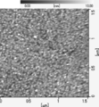
- FIG. 7 is an AFM photograph of the recess surface 128 of the channel layer 106 formed by the process shown in FIG. 6D.
- Microwave plasma process has excellent uniformity.
- the surface of the electron supply layer 110 is cleaned and flattened by the pretreatment using the first sacrificial layer 112.
- the arithmetic average roughness Ra of the recess surface 128 of the channel layer 106 is 0.5 nm or less
- the difference PV between the maximum peak height and the maximum valley depth of the sectional surface 128 is 10 nm or less
- the root mean square roughness RMS is either 1.1 nm or less. Therefore, dry etching of part of the electron supply layer 110 and the drift layer 108 can be performed uniformly.
- the arithmetic mean roughness Ra of the recess surface 128 is 0.4322 nm, and the difference PV between the maximum peak height and the maximum valley depth of the sectional curve is 5.618 nm.
- the root mean square RMS was 0.5494 nm.
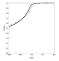
- FIG. 8 shows voltage-capacitance characteristics (CV characteristics) between the gate electrode 126 of the semiconductor device 100 manufactured by the manufacturing method according to the first and second embodiments and the channel layer 106.
- a broken line corresponds to the semiconductor device 100 manufactured in the first embodiment
- a solid line corresponds to the semiconductor device 100 manufactured in the second embodiment.
- the CV characteristic was measured at 1 MHz.
- the gate voltage (Vg) is 0 V
- C / Cox is 0.9.
- C / Cox exceeds 0.95.
- the slope of the CV characteristic curve is larger in the semiconductor device 100 manufactured in the second embodiment than in the semiconductor device 100 manufactured in the first embodiment. This indicates that the interface state density at the interface between the channel layer 106 and the gate insulating film 120 is lower in the semiconductor device 100 manufactured in the second embodiment than in the semiconductor device 100 manufactured in the first embodiment. .
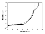
- FIG. 9 shows the JE characteristics of the semiconductor device 100 manufactured by the manufacturing method according to the first and second embodiments.
- the horizontal axis represents the channel field strength
- the vertical axis represents the channel current density.
- a broken line corresponds to the semiconductor device 100 manufactured in the first embodiment
- a solid line corresponds to the semiconductor device 100 manufactured in the second embodiment.
- the electric field intensity is started the current density rises from 4.5 MV / cm 2 around, breakdown phenomenon occurs at 11 MV / cm 2.
- the electric field strength is the current density from 6.5 MV / cm 2 near, the breakdown phenomenon occurs, the electric field strength is from beyond 12 MV / cm 2 .
- FIG. 10 shows transfer characteristics of the semiconductor device 100 manufactured by the manufacturing method according to the first and second embodiments.
- a broken line corresponds to the semiconductor device 100 manufactured in the first embodiment
- a solid line corresponds to the semiconductor device 100 manufactured in the second embodiment.
- the voltage (V ds ) between the source electrode 122 and the drain electrode 124 was 0.1 V
- the channel length was 6 ⁇ m
- the channel width was 0.84 mm.
- the channel lengths are the end portion of the drift layer 108 formed under the source electrode 122 near the gate electrode 126 side and the end portion of the drift layer 108 formed under the drain electrode 124 near the gate electrode 126 side. It corresponds to the length between.
- the gate voltage is 10 V
- the drain current is 0.37 mA
- the gate voltage is 15 V
- the drain current is 0.7 mA
- the gate voltage is 10 V
- the drain current is 0.5 mA
- the gate voltage is 15 V
- the drain current is 0.9 mA.
- FIG. 11 shows the field effect mobility of carriers in the semiconductor device 100 manufactured by the manufacturing method according to the first and second embodiments.
- a black square corresponds to the semiconductor device 100 manufactured in the first embodiment
- a white square in the black square corresponds to the semiconductor device 100 manufactured in the second embodiment.
- the voltage (V ds ) between the source electrode 122 and the drain electrode 124 was set to 0.1V.
- the channel length is 30 ⁇ m or more
- the carrier field-effect mobility exceeds 140 cm 2 / Vs
- the channel length is 50 ⁇ m
- the field-effect mobility is 160 cm 2 / Vs.
- the carrier field-effect mobility exceeds 140 cm 2 / Vs when the channel length is 15 ⁇ m or more, and the channel length is 30 ⁇ m and the field-effect mobility is 170 cm 2 / Vs. As described above, the channel length is 50 ⁇ m and the field-effect mobility is 190 cm 2 / Vs.
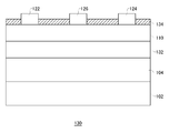
- FIG. 12 is a schematic cross-sectional view of an HFET 130 (GaN-based heterojunction field effect transistor) according to the third embodiment of the present invention.
- the HFET 130 includes a substrate 102, a buffer layer 104, an electron transit layer 132, an electron supply layer 110, an insulating layer 134, a source electrode 122, a drain electrode 124, and a gate electrode 126.
- the substrate 102 a silicon substrate having a (111) plane as a main surface may be used.
- a sapphire substrate, a SiC substrate, or a GaN substrate can also be used.
- the buffer layer 104 is formed on the substrate 102.
- the buffer layer 104 may be a semiconductor layer made of AlGaN.
- the electron transit layer 132 is formed on the buffer layer 104.
- the electron transit layer 132 may be a semiconductor layer made of GaN.
- the electron supply layer 110 is formed on the electron transit layer 132.
- the electron supply layer 110 may be a semiconductor layer made of Al 0.25 Ga 0.75 N. Two-dimensional electron gas is formed near the interface between the electron transit layer 132 and the electron supply layer 110.
- the source electrode 122, the drain electrode 124, and the gate electrode 126 are formed on part of the electron supply layer 110.
- the HFET 130 may be formed as follows. In the following description, elements described using the same reference numerals as in FIGS. 6A to 6E may have the same functions and configurations as the elements described in FIGS. 6A to 6E.
- the buffer layer 104, the electron transit layer 132, and the electron supply layer 110 are formed on the substrate 102. Thereafter, a first sacrificial layer having a higher solubility of impurities in the electron supply layer 110 than the electron supply layer 110 is formed in contact with the electron supply layer 110. After the electron supply layer 110 and the first sacrificial layer are annealed, the first sacrificial layer is removed by a wet process. Thereby, impurities in the electron supply layer 110 are removed, and the surface of the electron supply layer 110 is flattened.
- the pretreatment using the first sacrificial layer may be performed in the same manner as the manufacturing method according to the second embodiment.
- an insulating layer 134 is formed on the electron supply layer 110.
- the insulating layer 134 may be a SiO 2 film formed by a CVD method.
- the insulating layer 134 where the source electrode 122, the drain electrode 124, and the gate electrode 126 are to be formed is removed.
- the removal may be performed by dry etching using a microwave plasma process using a bromine-based etching gas.
- the microwave plasma process may be performed in the same manner as the manufacturing method according to the first embodiment. By the microwave plasma process using a bromine-based etching gas, the surface of the electron supply layer 110 is flattened, and the amount of halogen remaining on the surface is reduced.
- a source electrode 122, a drain electrode 124, and a gate electrode 126 are formed on the portion of the electron supply layer 110 from which the insulating layer 134 has been removed.
- the source electrode 122, the drain electrode 124, and the gate electrode 126 may be Ti / Al / Au formed by an evaporation method.
- the method for manufacturing the GaN-based MOS field effect transistor and the GaN-based heterojunction field effect transistor has been described.
- the present invention is not limited thereto, and other semiconductors including III-V group compound semiconductors are used.
- the sacrificial layer described in the manufacturing methods according to the first and second embodiments can also be applied to the MOS field effect transistor and the heterojunction field effect transistor.
- GaAs-based semiconductor devices such as GaAs and AlGaAs
- As is present on the surface of the GaAs-based semiconductor layer in excess of the stoichiometry and becomes an impurity.
- As oxide is present on the surface of the GaAs-based semiconductor layer.
- a sacrificial layer in which the solid solubility of impurities in the GaAs-based semiconductor layer is higher than that of the GaAs-based semiconductor layer may be formed on the GaAs-based semiconductor layer. After annealing the GaAs-based semiconductor layer and the sacrificial layer, the sacrificial layer can be removed by a wet process. Therefore, the surface of the GaAs-based semiconductor layer can be pretreated with the sacrificial layer, and the surface of the GaAs-based semiconductor layer can be made clean and flat.
- the sacrificial layer used for the GaAs-based semiconductor layer may be, for example, a polysilicon film or an amorphous silicon film in which the solid solubility of As is higher than that of the GaAs-based semiconductor layer.
- etching using microwave plasma and pretreatment using a sacrificial layer can be used in a manufacturing method of a semiconductor device such as a MISFET, a bipolar transistor, a Schottky diode, or the like.
- FIG. 13 shows a state in which the buffer layer 104, the channel layer 106, the drift layer 108, the electron supply layer 110, and the first sacrificial layer 112 are formed on the substrate 102. 13 that have the same reference numerals as those in FIG. 6B may have the same functions and configurations as the elements described in FIG. 6B.
- the buffer layer 104 is a composite layer in which GaN layers and AlN layers are alternately stacked.
- the channel layer 106 is made of p-type GaN.
- the drift layer 108 is made of u-GaN.
- the electron supply layer 110 is made of Al Y Ga 1-Y N (0 ⁇ Y ⁇ 1).
- the first sacrificial layer 112 is made of SiO 2 having a thickness of 60 nm. This configuration corresponds to a state in which the first sacrificial layer 112 is formed on the electron supply layer 110 illustrated in FIG. 6B.
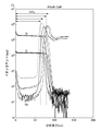
- the graph of FIG. 14 shows the result of measuring the distribution in the depth direction of silicon, oxygen and gallium atoms by SIMS analysis in the state shown in FIG. Cesium ions were used as primary ions for SIMS analysis.
- the horizontal axis of the graph represents the depth from the surface, and the vertical axis represents the ion count.
- an alternate long and two short dashes line indicates a result measured before the first sacrificial layer 112 is formed and annealed.
- the alternate long and short dash line shows the result of measurement in a state where the first sacrificial layer 112 was formed and annealed at 800 ° C. for 30 minutes in a nitrogen atmosphere.
- the first sacrificial layer 112 is removed with buffered hydrofluoric acid, the first sacrificial layer 112 is formed once again, and the result of SIMS analysis is shown by a solid line. Thereafter, the results of SIMS analysis after annealing in a nitrogen atmosphere at 800 ° C. for 30 minutes are shown by broken lines.
- the SIMS analysis result shown in FIG. 14 shows that the first sacrificial layer 112 is formed, the first sacrificial layer 112 and the electron supply layer 110 are annealed, and then the first sacrificial layer 112 is removed. Thus, the oxide on the surface of the electron supply layer 110 is removed.
- the result shows that by repeating the pretreatment using the first sacrificial layer 112, removal of impurities of Al Y Ga 1 -YN proceeds and the surface of the electron supply layer 110 becomes clean.
- FIG. 15 shows that a buffer layer 104 in which GaN layers and AlN layers are alternately stacked, a channel layer 106 made of p-type GaN, and a second sacrificial layer 118 made of SiO 2 having a thickness of 60 nm are formed on a substrate 102. Shows the state.
- elements denoted by the same reference numerals as those in FIG. 6E may have the same functions and configurations as the elements described in FIG. 6E.
- This structure corresponds to a state in which the second sacrificial layer 118 is formed on the recess surface 128 of the channel layer 106 shown in FIG. 6E.
- the graph of FIG. 16 shows the result of measuring the depth direction distribution of silicon, oxygen and gallium atoms by SIMS in the state shown in FIG.
- the SIMS analysis was performed in the same manner as the analysis shown in FIG.
- An alternate long and two short dashes line indicates a result of measurement before forming the second sacrificial layer 118 and performing annealing.
- the alternate long and short dash line shows the result of measurement with the second sacrificial layer 118 formed and annealed at 800 ° C. for 30 minutes in a nitrogen atmosphere.
- the second sacrificial layer 118 is removed with buffered hydrofluoric acid, and the second sacrificial layer 118 is formed once again.
- the result of SIMS analysis is shown by a solid line. Thereafter, the results of SIMS analysis after annealing in a nitrogen atmosphere at 800 ° C. for 30 minutes are shown by broken lines.
- the second sacrificial layer 118 is formed, the second sacrificial layer 118 and the channel layer 106 are annealed, and then the second sacrificial layer 118 is removed. This shows that the oxide on the surface of the channel layer 106 is removed.
- 100 semiconductor device 102 substrate, 104 buffer layer, 106 channel layer, 108 drift layer, 110 electron supply layer, 112 sacrificial layer, 114 mask layer, 116 recess portion, 118 sacrificial layer, 120 gate insulating film, 122 source electrode, 124 Drain electrode, 126 gate electrode, 128 recess surface, 130 HFET, 132 electron transit layer, 134 insulating layer, 250 microwave plasma device, 252 processing substrate, 254 stage, 256 dielectric, 258 processing chamber, 260 shower head, 262 antenna
Landscapes
- Junction Field-Effect Transistors (AREA)
- Insulated Gate Type Field-Effect Transistor (AREA)
- Chemical & Material Sciences (AREA)
- Drying Of Semiconductors (AREA)
- Thin Film Transistor (AREA)
- Recrystallisation Techniques (AREA)
- Chemical Kinetics & Catalysis (AREA)
- General Chemical & Material Sciences (AREA)
- Engineering & Computer Science (AREA)
- Materials Engineering (AREA)
Abstract
La présente invention concerne un procédé de production d'un dispositif à semi-conducteur produisant un dispositif à semi-conducteur à base de nitrure de gallium et comprenant : une étape de formation de première couche semi-conductrice formant une première couche semi-conductrice comprenant un semi-conducteur à base de nitrure de gallium ; et une étape de formation d'évidement effectuant la gravure sèche d'une partie de la première couche semi-conductrice par le biais d'un processus de plasma micro-ondes au moyen d'un gaz à base de brome, ce qui permet de former un évidement.
Priority Applications (3)
| Application Number | Priority Date | Filing Date | Title |
|---|---|---|---|
| EP12739117.5A EP2669933A4 (fr) | 2011-01-25 | 2012-01-23 | Dispositif à semi-conducteur à base de nitrure de gallium et procédé de production du dispositif à semi-conducteur |
| CN2012800049252A CN103299405A (zh) | 2011-01-25 | 2012-01-23 | 氮化镓系半导体装置及半导体装置的制造方法 |
| US13/950,079 US8999788B2 (en) | 2011-01-25 | 2013-07-24 | Manufacturing method of GaN-based semiconductor device and semiconductor device |
Applications Claiming Priority (2)
| Application Number | Priority Date | Filing Date | Title |
|---|---|---|---|
| JP2011-013425 | 2011-01-25 | ||
| JP2011013425A JP5841726B2 (ja) | 2011-01-25 | 2011-01-25 | 窒化ガリウム系半導体装置の製造方法 |
Related Child Applications (1)
| Application Number | Title | Priority Date | Filing Date |
|---|---|---|---|
| US13/950,079 Continuation US8999788B2 (en) | 2011-01-25 | 2013-07-24 | Manufacturing method of GaN-based semiconductor device and semiconductor device |
Publications (1)
| Publication Number | Publication Date |
|---|---|
| WO2012102011A1 true WO2012102011A1 (fr) | 2012-08-02 |
Family
ID=46580587
Family Applications (1)
| Application Number | Title | Priority Date | Filing Date |
|---|---|---|---|
| PCT/JP2012/000404 Ceased WO2012102011A1 (fr) | 2011-01-25 | 2012-01-23 | Dispositif à semi-conducteur à base de nitrure de gallium et procédé de production du dispositif à semi-conducteur |
Country Status (5)
| Country | Link |
|---|---|
| US (1) | US8999788B2 (fr) |
| EP (1) | EP2669933A4 (fr) |
| JP (1) | JP5841726B2 (fr) |
| CN (1) | CN103299405A (fr) |
| WO (1) | WO2012102011A1 (fr) |
Families Citing this family (9)
| Publication number | Priority date | Publication date | Assignee | Title |
|---|---|---|---|---|
| KR101455283B1 (ko) * | 2013-08-09 | 2014-10-31 | 홍익대학교 산학협력단 | 패시베이션막 형성방법 및 이를 포함하는 AlGaN/GaN HFET의 제조방법 |
| US9966519B2 (en) * | 2014-05-15 | 2018-05-08 | The Hong Kong University Of Science And Technology | Gallium nitride flip-chip light emitting diode |
| JP6950185B2 (ja) * | 2017-01-12 | 2021-10-13 | 三菱電機株式会社 | 高電子移動度トランジスタの製造方法、高電子移動度トランジスタ |
| CN111164733B (zh) * | 2017-07-20 | 2024-03-19 | 斯维甘公司 | 用于高电子迁移率晶体管的异质结构及其生产方法 |
| JP7112857B2 (ja) * | 2018-03-02 | 2022-08-04 | 株式会社サイオクス | GaN材料および半導体装置の製造方法 |
| JP7071893B2 (ja) * | 2018-07-23 | 2022-05-19 | 株式会社東芝 | 半導体装置及びその製造方法 |
| JP7107106B2 (ja) * | 2018-08-30 | 2022-07-27 | 富士電機株式会社 | 窒化ガリウム系半導体装置および窒化ガリウム系半導体装置の製造方法 |
| JP7084371B2 (ja) * | 2019-11-13 | 2022-06-14 | 株式会社サイオクス | 半導体装置、および、構造体の製造方法 |
| CN113005409B (zh) * | 2021-02-22 | 2022-09-13 | 延边大学 | 一种复合金属薄膜制备方法 |
Citations (6)
| Publication number | Priority date | Publication date | Assignee | Title |
|---|---|---|---|---|
| JPH0567592A (ja) * | 1991-09-10 | 1993-03-19 | Fujitsu Ltd | 半導体装置の製造方法 |
| JPH0823152A (ja) * | 1994-07-08 | 1996-01-23 | Mitsubishi Materials Corp | パターニング方法 |
| JP2007115752A (ja) * | 2005-10-18 | 2007-05-10 | Sumitomo Electric Ind Ltd | 窒化ガリウム系半導体領域にパターンを形成する方法 |
| JP2007235000A (ja) * | 2006-03-03 | 2007-09-13 | Eudyna Devices Inc | 半導体の処理方法、半導体装置およびその製造方法 |
| JP2010170974A (ja) * | 2008-12-22 | 2010-08-05 | Tokyo Electron Ltd | プラズマ源およびプラズマ処理装置 |
| JP2010272728A (ja) * | 2009-05-22 | 2010-12-02 | Furukawa Electric Co Ltd:The | GaN系半導体素子およびその製造方法 |
Family Cites Families (1)
| Publication number | Priority date | Publication date | Assignee | Title |
|---|---|---|---|---|
| JP5566670B2 (ja) * | 2008-12-16 | 2014-08-06 | 古河電気工業株式会社 | GaN系電界効果トランジスタ |
-
2011
- 2011-01-25 JP JP2011013425A patent/JP5841726B2/ja active Active
-
2012
- 2012-01-23 CN CN2012800049252A patent/CN103299405A/zh active Pending
- 2012-01-23 EP EP12739117.5A patent/EP2669933A4/fr not_active Withdrawn
- 2012-01-23 WO PCT/JP2012/000404 patent/WO2012102011A1/fr not_active Ceased
-
2013
- 2013-07-24 US US13/950,079 patent/US8999788B2/en active Active
Patent Citations (6)
| Publication number | Priority date | Publication date | Assignee | Title |
|---|---|---|---|---|
| JPH0567592A (ja) * | 1991-09-10 | 1993-03-19 | Fujitsu Ltd | 半導体装置の製造方法 |
| JPH0823152A (ja) * | 1994-07-08 | 1996-01-23 | Mitsubishi Materials Corp | パターニング方法 |
| JP2007115752A (ja) * | 2005-10-18 | 2007-05-10 | Sumitomo Electric Ind Ltd | 窒化ガリウム系半導体領域にパターンを形成する方法 |
| JP2007235000A (ja) * | 2006-03-03 | 2007-09-13 | Eudyna Devices Inc | 半導体の処理方法、半導体装置およびその製造方法 |
| JP2010170974A (ja) * | 2008-12-22 | 2010-08-05 | Tokyo Electron Ltd | プラズマ源およびプラズマ処理装置 |
| JP2010272728A (ja) * | 2009-05-22 | 2010-12-02 | Furukawa Electric Co Ltd:The | GaN系半導体素子およびその製造方法 |
Non-Patent Citations (1)
| Title |
|---|
| See also references of EP2669933A4 * |
Also Published As
| Publication number | Publication date |
|---|---|
| JP5841726B2 (ja) | 2016-01-13 |
| CN103299405A (zh) | 2013-09-11 |
| US8999788B2 (en) | 2015-04-07 |
| EP2669933A4 (fr) | 2015-05-13 |
| EP2669933A1 (fr) | 2013-12-04 |
| JP2012156263A (ja) | 2012-08-16 |
| US20130307063A1 (en) | 2013-11-21 |
Similar Documents
| Publication | Publication Date | Title |
|---|---|---|
| JP5841726B2 (ja) | 窒化ガリウム系半導体装置の製造方法 | |
| CN107946358B (zh) | 一种与Si-CMOS工艺兼容的AlGaN/GaN异质结HEMT器件及其制作方法 | |
| CN101211969B (zh) | 高速大功率氮化物半导体器件及其制造方法 | |
| JP5697012B2 (ja) | 溝の形成方法、および電界効果トランジスタの製造方法 | |
| KR101439015B1 (ko) | 반도체 장치 및 반도체 장치의 제조 방법 | |
| CN105655395B (zh) | 一种增强型高电子迁移率晶体管及其制作方法 | |
| CN103035703B (zh) | 化合物半导体器件及其制造方法 | |
| CN114521293B (zh) | 半导体装置及半导体装置的制造方法 | |
| WO2019009111A1 (fr) | Dispositif semi-conducteur et son procédé de production | |
| CN106257686A (zh) | 半导体器件及其制造方法 | |
| JP5506055B2 (ja) | 半導体装置の製造方法 | |
| KR101688965B1 (ko) | 반도체 소자 제조방법 | |
| JP6152700B2 (ja) | 半導体装置の製造方法 | |
| CN117199124A (zh) | 功率器件外延结构及其制备方法、功率器件 | |
| JP6028970B2 (ja) | 半導体装置の製造方法およびエッチング方法 | |
| CN106409901B (zh) | 一种半导体器件及其制备方法 | |
| CN116845111A (zh) | 一种双终端氮化镓基二极管及其制备方法 | |
| JP6019558B2 (ja) | 窒化物電子デバイス、窒化物電子デバイスを作製する方法 | |
| KR101952176B1 (ko) | 인헨스먼트 질화물 반도체 소자 및 이의 제조 방법 | |
| CN108695156A (zh) | 改善ⅲ族氮化物mis-hemt欧姆接触的方法及mis-hemt器件 | |
| JP2013187285A (ja) | エピタキシャルウェハの製造方法 | |
| JP5619854B2 (ja) | 電界効果トランジスタ | |
| JP2012004444A (ja) | 半導体装置の製造方法 | |
| JP2011061094A (ja) | 電界効果トランジスタの製造方法 | |
| JP2013131651A (ja) | 半導体装置の製造方法 |
Legal Events
| Date | Code | Title | Description |
|---|---|---|---|
| 121 | Ep: the epo has been informed by wipo that ep was designated in this application |
Ref document number: 12739117 Country of ref document: EP Kind code of ref document: A1 |
|
| WWE | Wipo information: entry into national phase |
Ref document number: 2012739117 Country of ref document: EP |
|
| NENP | Non-entry into the national phase |
Ref country code: DE |