WO2012102043A1 - Procédé de commande de panneau d'affichage à plasma et dispositif d'affichage à plasma - Google Patents
Procédé de commande de panneau d'affichage à plasma et dispositif d'affichage à plasma Download PDFInfo
- Publication number
- WO2012102043A1 WO2012102043A1 PCT/JP2012/000484 JP2012000484W WO2012102043A1 WO 2012102043 A1 WO2012102043 A1 WO 2012102043A1 JP 2012000484 W JP2012000484 W JP 2012000484W WO 2012102043 A1 WO2012102043 A1 WO 2012102043A1
- Authority
- WO
- WIPO (PCT)
- Prior art keywords
- voltage
- subfield
- discharge
- scan electrode
- sustain
- Prior art date
- Legal status (The legal status is an assumption and is not a legal conclusion. Google has not performed a legal analysis and makes no representation as to the accuracy of the status listed.)
- Ceased
Links
Images


Classifications
-
- G—PHYSICS
- G09—EDUCATION; CRYPTOGRAPHY; DISPLAY; ADVERTISING; SEALS
- G09G—ARRANGEMENTS OR CIRCUITS FOR CONTROL OF INDICATING DEVICES USING STATIC MEANS TO PRESENT VARIABLE INFORMATION
- G09G3/00—Control arrangements or circuits, of interest only in connection with visual indicators other than cathode-ray tubes
- G09G3/20—Control arrangements or circuits, of interest only in connection with visual indicators other than cathode-ray tubes for presentation of an assembly of a number of characters, e.g. a page, by composing the assembly by combination of individual elements arranged in a matrix no fixed position being assigned to or needed to be assigned to the individual characters or partial characters
- G09G3/22—Control arrangements or circuits, of interest only in connection with visual indicators other than cathode-ray tubes for presentation of an assembly of a number of characters, e.g. a page, by composing the assembly by combination of individual elements arranged in a matrix no fixed position being assigned to or needed to be assigned to the individual characters or partial characters using controlled light sources
- G09G3/28—Control arrangements or circuits, of interest only in connection with visual indicators other than cathode-ray tubes for presentation of an assembly of a number of characters, e.g. a page, by composing the assembly by combination of individual elements arranged in a matrix no fixed position being assigned to or needed to be assigned to the individual characters or partial characters using controlled light sources using luminous gas-discharge panels, e.g. plasma panels
- G09G3/288—Control arrangements or circuits, of interest only in connection with visual indicators other than cathode-ray tubes for presentation of an assembly of a number of characters, e.g. a page, by composing the assembly by combination of individual elements arranged in a matrix no fixed position being assigned to or needed to be assigned to the individual characters or partial characters using controlled light sources using luminous gas-discharge panels, e.g. plasma panels using AC panels
- G09G3/291—Control arrangements or circuits, of interest only in connection with visual indicators other than cathode-ray tubes for presentation of an assembly of a number of characters, e.g. a page, by composing the assembly by combination of individual elements arranged in a matrix no fixed position being assigned to or needed to be assigned to the individual characters or partial characters using controlled light sources using luminous gas-discharge panels, e.g. plasma panels using AC panels controlling the gas discharge to control a cell condition, e.g. by means of specific pulse shapes
- G09G3/292—Control arrangements or circuits, of interest only in connection with visual indicators other than cathode-ray tubes for presentation of an assembly of a number of characters, e.g. a page, by composing the assembly by combination of individual elements arranged in a matrix no fixed position being assigned to or needed to be assigned to the individual characters or partial characters using controlled light sources using luminous gas-discharge panels, e.g. plasma panels using AC panels controlling the gas discharge to control a cell condition, e.g. by means of specific pulse shapes for reset discharge, priming discharge or erase discharge occurring in a phase other than addressing
- G09G3/2927—Details of initialising
-
- G—PHYSICS
- G09—EDUCATION; CRYPTOGRAPHY; DISPLAY; ADVERTISING; SEALS
- G09G—ARRANGEMENTS OR CIRCUITS FOR CONTROL OF INDICATING DEVICES USING STATIC MEANS TO PRESENT VARIABLE INFORMATION
- G09G3/00—Control arrangements or circuits, of interest only in connection with visual indicators other than cathode-ray tubes
- G09G3/20—Control arrangements or circuits, of interest only in connection with visual indicators other than cathode-ray tubes for presentation of an assembly of a number of characters, e.g. a page, by composing the assembly by combination of individual elements arranged in a matrix no fixed position being assigned to or needed to be assigned to the individual characters or partial characters
- G09G3/22—Control arrangements or circuits, of interest only in connection with visual indicators other than cathode-ray tubes for presentation of an assembly of a number of characters, e.g. a page, by composing the assembly by combination of individual elements arranged in a matrix no fixed position being assigned to or needed to be assigned to the individual characters or partial characters using controlled light sources
- G09G3/28—Control arrangements or circuits, of interest only in connection with visual indicators other than cathode-ray tubes for presentation of an assembly of a number of characters, e.g. a page, by composing the assembly by combination of individual elements arranged in a matrix no fixed position being assigned to or needed to be assigned to the individual characters or partial characters using controlled light sources using luminous gas-discharge panels, e.g. plasma panels
- G09G3/288—Control arrangements or circuits, of interest only in connection with visual indicators other than cathode-ray tubes for presentation of an assembly of a number of characters, e.g. a page, by composing the assembly by combination of individual elements arranged in a matrix no fixed position being assigned to or needed to be assigned to the individual characters or partial characters using controlled light sources using luminous gas-discharge panels, e.g. plasma panels using AC panels
- G09G3/291—Control arrangements or circuits, of interest only in connection with visual indicators other than cathode-ray tubes for presentation of an assembly of a number of characters, e.g. a page, by composing the assembly by combination of individual elements arranged in a matrix no fixed position being assigned to or needed to be assigned to the individual characters or partial characters using controlled light sources using luminous gas-discharge panels, e.g. plasma panels using AC panels controlling the gas discharge to control a cell condition, e.g. by means of specific pulse shapes
- G09G3/294—Control arrangements or circuits, of interest only in connection with visual indicators other than cathode-ray tubes for presentation of an assembly of a number of characters, e.g. a page, by composing the assembly by combination of individual elements arranged in a matrix no fixed position being assigned to or needed to be assigned to the individual characters or partial characters using controlled light sources using luminous gas-discharge panels, e.g. plasma panels using AC panels controlling the gas discharge to control a cell condition, e.g. by means of specific pulse shapes for lighting or sustain discharge
-
- G—PHYSICS
- G09—EDUCATION; CRYPTOGRAPHY; DISPLAY; ADVERTISING; SEALS
- G09G—ARRANGEMENTS OR CIRCUITS FOR CONTROL OF INDICATING DEVICES USING STATIC MEANS TO PRESENT VARIABLE INFORMATION
- G09G3/00—Control arrangements or circuits, of interest only in connection with visual indicators other than cathode-ray tubes
- G09G3/20—Control arrangements or circuits, of interest only in connection with visual indicators other than cathode-ray tubes for presentation of an assembly of a number of characters, e.g. a page, by composing the assembly by combination of individual elements arranged in a matrix no fixed position being assigned to or needed to be assigned to the individual characters or partial characters
- G09G3/22—Control arrangements or circuits, of interest only in connection with visual indicators other than cathode-ray tubes for presentation of an assembly of a number of characters, e.g. a page, by composing the assembly by combination of individual elements arranged in a matrix no fixed position being assigned to or needed to be assigned to the individual characters or partial characters using controlled light sources
- G09G3/28—Control arrangements or circuits, of interest only in connection with visual indicators other than cathode-ray tubes for presentation of an assembly of a number of characters, e.g. a page, by composing the assembly by combination of individual elements arranged in a matrix no fixed position being assigned to or needed to be assigned to the individual characters or partial characters using controlled light sources using luminous gas-discharge panels, e.g. plasma panels
- G09G3/288—Control arrangements or circuits, of interest only in connection with visual indicators other than cathode-ray tubes for presentation of an assembly of a number of characters, e.g. a page, by composing the assembly by combination of individual elements arranged in a matrix no fixed position being assigned to or needed to be assigned to the individual characters or partial characters using controlled light sources using luminous gas-discharge panels, e.g. plasma panels using AC panels
- G09G3/296—Driving circuits for producing the waveforms applied to the driving electrodes
- G09G3/2965—Driving circuits for producing the waveforms applied to the driving electrodes using inductors for energy recovery
-
- G—PHYSICS
- G09—EDUCATION; CRYPTOGRAPHY; DISPLAY; ADVERTISING; SEALS
- G09G—ARRANGEMENTS OR CIRCUITS FOR CONTROL OF INDICATING DEVICES USING STATIC MEANS TO PRESENT VARIABLE INFORMATION
- G09G2310/00—Command of the display device
- G09G2310/06—Details of flat display driving waveforms
- G09G2310/066—Waveforms comprising a gently increasing or decreasing portion, e.g. ramp
Definitions
- the present invention relates to a plasma display device using an AC surface discharge type plasma display panel and a driving method of the plasma display panel.
- a typical AC surface discharge type panel as a plasma display panel (hereinafter abbreviated as “panel”) has a large number of discharge cells formed between a front substrate and a rear substrate that are arranged to face each other.
- a plurality of pairs of display electrodes composed of a pair of scan electrodes and sustain electrodes are formed in parallel with each other on the front glass substrate.
- a dielectric layer and a protective layer are formed so as to cover the display electrode pairs.
- the back substrate has a plurality of parallel data electrodes formed on the glass substrate on the back side, a dielectric layer is formed so as to cover the data electrodes, and a plurality of barrier ribs are formed thereon in parallel with the data electrodes. ing. And the fluorescent substance layer is formed in the surface of a dielectric material layer, and the side surface of a partition.
- the front substrate and the rear substrate are arranged opposite to each other and sealed so that the display electrode pair and the data electrode are three-dimensionally crossed.
- a discharge gas containing xenon at a partial pressure ratio of 5% is sealed, and a discharge cell is formed in a portion where the display electrode pair and the data electrode face each other.
- ultraviolet rays are generated by gas discharge in each discharge cell, and the phosphors of each color of red (R), green (G) and blue (B) are excited and emitted by the ultraviolet rays. Display an image.
- a subfield method is generally used as a method for displaying an image in an image display area of a panel by combining binary control of light emission and non-light emission in a discharge cell.
- each discharge cell In the subfield method, one field is divided into a plurality of subfields having different emission luminances.
- each discharge cell light emission / non-light emission of each subfield is controlled by a combination according to a desired gradation value.
- each discharge cell emits light with the emission luminance of one field set to a desired gradation value, and an image composed of various combinations of gradation values is displayed in the image display area of the panel.
- each subfield has an initialization period, an address period, and a sustain period.
- an initialization waveform is applied to each scan electrode, and an initialization operation is performed to generate an initialization discharge in each discharge cell.
- wall charges necessary for the subsequent address operation are formed, and priming particles (excited particles for generating the discharge) for generating the address discharge stably are generated.
- the scan pulse is sequentially applied to the scan electrodes, and the address pulse is selectively applied to the data electrodes based on the image signal to be displayed.
- an address discharge is generated between the scan electrode and the data electrode of the discharge cell to emit light, and a wall charge is formed in the discharge cell (hereinafter, these operations are also collectively referred to as “address”). ).
- the number of sustain pulses based on the luminance weight determined for each subfield is alternately applied to the display electrode pairs composed of the scan electrodes and the sustain electrodes.
- a sustain discharge is generated in the discharge cell that has generated the address discharge, and the phosphor layer of the discharge cell emits light (hereinafter referred to as “lighting” that the discharge cell emits light by the sustain discharge, and “non-emitting”). Also written as “lit”.)
- each discharge cell is made to emit light with the luminance according to the luminance weight.
- each discharge cell of the panel is caused to emit light with a luminance corresponding to the gradation value of the image signal, and an image is displayed in the image display area of the panel.
- One of the important factors in improving the image display quality on the panel is the improvement in contrast.
- a driving method for reducing the light emission not related to gradation display as much as possible and improving the contrast ratio is disclosed (for example, see Patent Document 1).
- a forced initializing operation in which initializing discharge is generated in all discharge cells using a ramp waveform voltage that gradually increases in voltage, and a sustain discharge is generated in the sustain period of the immediately preceding subfield. Any initializing operation of the selective initializing operation for selectively generating the initializing discharge with respect to the discharged cells is performed. Then, the number of times of performing the forced initializing operation is once per field, and the selective initializing operation is performed in the initializing period of the other subfield.
- black luminance The luminance of the black display area where no sustain discharge occurs (hereinafter abbreviated as “black luminance”) varies depending on light emission not related to image display, for example, light emission caused by initialization discharge.
- light emission in the black display region is only weak light emission when the forced initializing operation for generating the initializing discharge in all the discharge cells is performed. As a result, it is possible to reduce the black luminance and display an image with high contrast.
- the display electrode pairs are divided into a plurality of groups, and the number of times of performing the forced initializing operation is once in a plurality of fields, thereby further reducing the light emission not related to the gradation display and further reducing the black luminance.
- a driving method for further improving the above is also disclosed (for example, see Patent Document 2).
- the forced initialization operation has a function of accumulating wall charges necessary for generating an address discharge in the discharge cell in the subsequent address period.
- it has a function of generating priming particles for shortening the discharge delay time to surely generate the address discharge.
- This discharge delay time is the time required for the actual discharge to occur after the voltage applied to the discharge cell exceeds the discharge start voltage. The longer the discharge delay time, the more unstable the generation of discharge. .
- the wall charge and priming particles necessary to generate the address discharge are insufficient, the address discharge delay time becomes long, and the address operation becomes unstable. Or, there is a risk of malfunction such as no occurrence of address discharge.
- the sustain discharge does not occur in the discharge cell displaying black, the priming particles are likely to be insufficient, and the address operation is likely to be unstable. Such a phenomenon is likely to occur in a panel with high definition and a finer discharge cell structure.
- the present invention relates to a panel having a plurality of discharge cells each having a display electrode pair consisting of a scan electrode and a sustain electrode and a data electrode, and selectively initializing the scan electrode with a falling ramp waveform voltage that decreases toward a negative voltage.
- This is a panel driving method in which a subfield having an initialization period in which an operation is performed, an address period, and a sustain period in which a number of sustain pulses corresponding to a luminance weight are applied to a display electrode pair is provided in one field.
- an upward ramp waveform voltage for generating an erasing discharge in the discharge cells is applied to the scan electrodes after the last sustain pulse is generated in the sustain period.
- the maximum voltage of the upward ramp waveform voltage is The voltage is set to a voltage higher than the maximum voltage of the upward ramp waveform voltage generated in the subfield having a relatively small luminance weight.
- a forced initialization operation in which an up-slope waveform voltage and a down-slope waveform voltage are applied to the scan electrode and a selective initialization operation in which a down-slope waveform voltage is applied to the scan electrode are mixed.
- the specific cell initialization period may be provided, and the initialization period of the subfield having the relatively small luminance weight may be set as the specific cell initialization period.
- the subfield having the relatively large luminance weight and the subfield having the relatively small luminance weight may be continuously generated in the same field.
- the voltage applied to the scan electrode is decreased once before the voltage applied to the scan electrode is increased, and the voltage applied to the scan electrode is again reduced. It may be generated by raising.
- the present invention also provides a panel having a plurality of discharge cells each having a display electrode pair consisting of a scan electrode and a sustain electrode and a data electrode, and a selection to apply a downward ramp waveform voltage that decreases toward a negative voltage to the scan electrode.
- the drive circuit applies an upward ramp waveform voltage for generating an erasing discharge to the discharge cells after the generation of the last sustain pulse in the sustain period to the scan electrodes.
- the maximum voltage of the upward ramp waveform voltage is The voltage is set to a voltage higher than the maximum voltage of the upward ramp waveform voltage generated in the subfield having a relatively small luminance weight.
- the driving circuit includes a forced initializing operation for applying the rising ramp waveform voltage and the falling ramp waveform voltage to the scan electrode, and a selective initialization operation for applying the falling ramp waveform voltage to the scan electrode. May be provided, and the initialization period of the subfield having a relatively small luminance weight may be set as the specific cell initialization period.
- the driving circuit continuously generates the subfield having the relatively large luminance weight and the subfield having the relatively small luminance weight in the same field. May be.
- the driving circuit decreases the applied voltage to the scan electrode once before the applied voltage to the scan electrode rises to the maximum voltage, and again, It may be generated by increasing the voltage applied to the scan electrode.
- FIG. 1 is an exploded perspective view showing a structure of a panel used in the plasma display device in accordance with the first exemplary embodiment of the present invention.
- FIG. 2 is an electrode array diagram of the panel used in the plasma display device in accordance with the first exemplary embodiment of the present invention.
- FIG. 3 is a diagram showing a driving voltage waveform applied to each electrode of the panel used in the plasma display device in accordance with the first exemplary embodiment of the present invention.
- FIG. 4 is a circuit block diagram of the plasma display device in accordance with the first exemplary embodiment of the present invention.
- FIG. 5 is a circuit diagram schematically showing a configuration of a scan electrode driving circuit of the plasma display device in accordance with the first exemplary embodiment of the present invention.
- FIG. 1 is an exploded perspective view showing a structure of a panel used in the plasma display device in accordance with the first exemplary embodiment of the present invention.
- FIG. 2 is an electrode array diagram of the panel used in the plasma display device in accordance with the first exemplary embodiment of the
- FIG. 6 is a timing chart for explaining the operation of the driving circuit of the plasma display device in accordance with the first exemplary embodiment of the present invention.
- FIG. 7 is a diagram showing a driving voltage waveform applied to each electrode of the panel used in the plasma display device in accordance with the second exemplary embodiment of the present invention.
- FIG. 1 is an exploded perspective view showing the structure of panel 10 used in the plasma display device in accordance with the first exemplary embodiment of the present invention.
- a plurality of display electrode pairs 24 each including a scanning electrode 22 and a sustaining electrode 23 are formed on a glass front substrate 21.
- a dielectric layer 25 is formed so as to cover the scan electrode 22 and the sustain electrode 23, and a protective layer 26 is formed on the dielectric layer 25.
- the protective layer 26 is formed of a material mainly composed of magnesium oxide (MgO), which is a material having high electron emission performance, in order to easily generate discharge in the discharge cell.
- MgO magnesium oxide
- the protective layer 26 may be composed of a single layer or may be composed of a plurality of layers. Moreover, the structure which particle
- a plurality of data electrodes 32 are formed on the rear substrate 31, a dielectric layer 33 is formed so as to cover the data electrodes 32, and a grid-like partition wall 34 is formed thereon.
- a phosphor layer 35 that emits light of each color of red (R), green (G), and blue (B) is provided on the side surface of the partition wall 34 and on the dielectric layer 33.
- the front substrate 21 and the rear substrate 31 are arranged to face each other so that the display electrode pair 24 and the data electrode 32 intersect each other with a minute discharge space interposed therebetween, and a discharge space is formed in the gap between the front substrate 21 and the rear substrate 31.
- the outer peripheral part is sealed with sealing materials, such as glass frit. Then, for example, a mixed gas of neon (Ne) and xenon (Xe) is sealed in the discharge space inside as a discharge gas.
- the discharge space is divided into a plurality of sections by partition walls 34, and discharge cells constituting pixels are formed at the intersections of the display electrode pairs 24 and the data electrodes 32.
- a color image is displayed on the panel 10 by discharging and emitting (lighting) these discharge cells.
- One pixel is composed of three discharge cells, ie, discharge cells emitting blue (B).
- the structure of the panel 10 is not limited to the above-described structure, and may be, for example, provided with a stripe-shaped partition wall.
- FIG. 2 is an electrode array diagram of panel 10 used in the plasma display device in accordance with the first exemplary embodiment of the present invention.
- the panel 10 includes n scan electrodes SC1 to SCn (scan electrode 22 in FIG. 1) extended in the horizontal direction (row direction and line direction) and n sustain electrodes SU1 to SUn (FIG. 1). Are arranged, and m data electrodes D1 to Dm (data electrode 32 in FIG. 1) extending in the vertical direction (column direction) are arranged.
- the plasma display device in this embodiment performs gradation display by a subfield method.
- the subfield method one field is divided into a plurality of subfields on the time axis, and a luminance weight is set for each subfield.
- Each subfield has an initialization period, an address period, and a sustain period.
- An image is displayed on the panel 10 by controlling light emission / non-light emission of each discharge cell for each subfield.
- the luminance weight represents a ratio of the luminance magnitudes displayed in each subfield, and the number of sustain pulses corresponding to the luminance weight is generated in the sustain period in each subfield. Therefore, for example, the subfield with the luminance weight “8” emits light with a luminance about eight times that of the subfield with the luminance weight “1”, and emits light with about four times the luminance of the subfield with the luminance weight “2”. Therefore, various gradations can be displayed and images can be displayed by selectively causing each subfield to emit light in a combination according to the image signal.
- one field is divided into 10 subfields (subfield SF1, subfield SF2,..., Subfield SF10), and the luminance weight increases in the later subfield.
- each subfield has a luminance weight of (1, 2, 3, 6, 11, 18, 30, 44, 60, 80).
- a red image signal (R signal), a green image signal (G signal), and a blue image signal (B signal) are displayed in 256 gradations from 0 to 255, respectively. Can do.
- the initializing operation at this time includes a forced initializing operation in which initializing discharge is generated in all the discharge cells, and an initializing discharge selectively with respect to the discharge cells in which the sustain discharge is generated in the sustain period of the immediately preceding subfield. And a selective initialization operation that generates
- an address operation is performed in which an address discharge is selectively generated in the discharge cells to emit light to form wall charges necessary for the sustain discharge.
- a number of sustain pulses corresponding to the luminance weight determined in advance for each subfield are alternately applied to the display electrode pair 24 to generate a sustain discharge in the discharge cell in which the address discharge is generated.
- a sustain operation for emitting light from the cell is performed.
- the “specific cell initialization operation” is performed in the initialization period of one subfield, and all the subfields in the initialization period of the other subfields.
- a selective initialization operation is performed in the discharge cell.
- the specific cell initializing operation is an initializing operation in which a forced initializing operation is performed in a specific discharge cell and a selective initializing operation is performed in another discharge cell. Therefore, in the initialization period in which the specific cell initializing operation is performed, an initializing waveform for performing the forced initializing operation is applied to the specific discharge cell, and the initial stage for performing the selective initializing operation is performed on the other discharge cells. Apply the waveform.
- the initialization waveform for performing the forced initialization operation is referred to as “forced initialization waveform”
- the initialization waveform for performing the selective initialization operation is referred to as “selective initialization waveform”.
- An initialization period in which the specific cell initialization operation is performed is referred to as a “specific cell initialization period”
- a subfield having the specific cell initialization period is referred to as a “specific cell initialization subfield”.
- an initialization period in which a selective initialization operation is performed in all discharge cells is referred to as a “selective initialization period”
- a subfield having the selective initialization period is referred to as a “selective initialization subfield”.
- the first subfield (subfield SF1) of each field is a specific cell initialization subfield
- the other subfields (subfield SF2 to subfield SF10) are selective initialization subfields. .
- the luminance weight is increased in the field as the subfield occurs later in time.
- one field includes one subfield group including a plurality of subfields whose luminance weight increases as the subfield occurs later in time.
- the number of subfields constituting one field and the luminance weight of each subfield are not limited to the above values.
- the structure which switches a subfield structure based on an image signal etc. may be sufficient.
- FIG. 3 is a diagram showing drive voltage waveforms applied to the respective electrodes of panel 10 used in the plasma display device in accordance with the first exemplary embodiment of the present invention.
- FIG. 3 shows scan electrode SC1 that performs the address operation first in the address period, scan electrode SC2 that performs the address operation second in the address period, sustain electrode SU1 to sustain electrode SUn, and data electrode D1 to data electrode Dm.
- the drive voltage waveform applied to is shown.
- FIG. 3 shows drive voltage waveforms in a subfield SF1 which is a specific cell initialization subfield and subfields SF2 and subsequent subfields SF2 which are selective initialization subfields.
- the specific cell initialization subfield and the selective initialization subfield differ in the waveform shape of the drive voltage applied to scan electrode SC1 through scan electrode SCn in the initialization period 2.
- FIG. 3 shows two fields.
- a forced initializing waveform is applied to scan electrode SC1 and a selective initializing waveform is applied to scan electrode SC2 in the initializing period (specific cell initializing period) of subfield SF1, which is a specific cell initializing subfield.
- a forced initializing waveform is applied to scan electrode SC2 during the initializing period of subfield SF1
- a selective initializing waveform is applied to scan electrode SC1.
- the drive voltage waveform in the subfield after subfield SF3 is substantially the same as the drive voltage waveform in subfield SF2 except that the number of sustain pulses generated in the sustain period is different.
- the waveform shape of the rising ramp waveform voltage for generating the erasing discharge is different from the rising ramp waveform voltage for generating the erasing discharge in the other subfields. Details of this will be described later.
- scan electrode SCi, sustain electrode SUi, and data electrode Dk in the following represent electrodes selected from each electrode based on image data (data indicating lighting / non-lighting for each subfield).
- subfield SF1 which is a specific cell initialization subfield
- the first, third, fifth,... A forced initialization waveform for performing a forced initialization operation is applied to the (1 + 2 ⁇ N) th (N is an integer of 0 or more) scan electrode SC (1 + 2 ⁇ N). Then, the second, fourth, sixth,... From the top in terms of arrangement, the (2 + 2 ⁇ N) th (N is an integer of 0 or more) scan electrode SC (2 + 2 ⁇ N). Applies a selective initialization waveform for performing a selective initialization operation.
- the (2 + 2 ⁇ N) th (2, +4, 6th,...
- a forced initialization waveform for performing a forced initialization operation is applied to scan electrodes SC (2 + 2 ⁇ N), where N is an integer of 0 or more.
- the (1 + 2 ⁇ N) th (N is an integer of 0 or more) scan electrode SC (1 + 2 ⁇ N).
- FIG. 3 shows the scan electrode SC1 as a representative example of the scan electrode SC (1 + 2 ⁇ N), and the scan electrode SC2 as a representative example of the scan electrode SC (2 + 2 ⁇ N).
- the voltage 0 (V) is applied to the data electrodes D1 to Dm, and the voltage 0 (V) is applied to the sustain electrodes SU1 to SUn. ) Is applied.
- Scan electrode SC (1 + 2 ⁇ N) (for example, scan electrode SC1) to which a forced initialization waveform is applied is applied is applied with voltage Vi1 after voltage 0 (V) is applied, and gradually from voltage Vi1 to voltage Vi2.
- Apply a rising ramp waveform voltage (eg, with a slope of about 5 V / ⁇ sec).
- the voltage Vi1 is set to a voltage lower than the discharge start voltage with respect to the sustain electrode SU (1 + 2 ⁇ N) (that is, a voltage at which no discharge occurs in the discharge cell), and the voltage Vi2 is set to the sustain electrode SU (1 + 2).
- XN is set to a voltage exceeding the discharge start voltage (that is, a voltage at which discharge occurs in the discharge cell regardless of whether there is a previous discharge).
- negative wall voltage is accumulated on scan electrode SC (1 + 2 ⁇ N), and on data electrode D1 to data electrode Dm and sustain electrode SU (1 + 2 ⁇ N) intersecting scan electrode SC (1 + 2 ⁇ N).
- the positive wall voltage is accumulated in.
- priming particles that shorten the discharge delay time of the address discharge (the length of time from when the voltage applied to the discharge cell exceeds the discharge start voltage to when the discharge occurs in the discharge cell) are also generated.
- the wall voltage on the electrode represents a voltage generated by wall charges accumulated on the dielectric layer 25 covering the electrode, the protective layer 26, the phosphor layer 35, and the like.
- the positive voltage Ve is applied to the sustain electrodes SU1 to SUn, and the voltage 0 (V) is applied to the data electrodes D1 to Dm.
- Scan electrode SC (1 + 2 ⁇ N) (for example, scan electrode SC1, scan electrode SC3, scan electrode SC5,...) Gradually (eg, about ⁇ 2.5 V) from voltage Vi3 to negative voltage Vi4. Apply a falling ramp waveform voltage (with a slope of / ⁇ sec).
- the voltage Vi3 is set to a voltage lower than the discharge start voltage with respect to the sustain electrode SU (1 + 2 ⁇ N), and the voltage Vi4 is set to a voltage higher than the discharge start voltage with respect to the sustain electrode SU (1 + 2 ⁇ N).
- the positive wall voltage on the data electrode Dm is adjusted to a voltage suitable for the write operation in the write period. Furthermore, priming particles that shorten the discharge delay time of the address discharge are also generated.
- the above voltage waveform is a forced initializing waveform that generates an initializing discharge in the discharge cell regardless of the operation of the immediately preceding subfield.
- the operation for applying the forced initialization waveform to the scan electrode 22 is the forced initialization operation.
- the initialization operation in the discharge cell formed on the (1 + 2 ⁇ N) -th scan electrode SC (1 + 2 ⁇ N) from the top is the previous sub-field SF1.
- the forced initializing operation generates an initializing discharge in the discharge cells regardless of the field operation.
- voltage Vi1 is applied to scan electrode SC (2 + 2 ⁇ N) (for example, scan electrode SC2, scan electrode SC4, scan electrode SC6,...) In the first half of initialization period Ti1 of subfield SF1.
- an upward ramp waveform voltage that gently rises from the voltage 0 (V) toward the voltage Vi5 is applied.
- This upward ramp waveform voltage is a voltage waveform that continues to rise for the same time at the same gradient as the upward ramp waveform voltage applied to scan electrode SC (1 + 2 ⁇ N). Therefore, the voltage Vi5 is equal to the voltage obtained by subtracting the voltage Vi1 from the voltage Vi2.
- each voltage is set so that the voltage Vi5 is lower than the discharge start voltage with respect to the sustain electrode SU (2 + 2 ⁇ N). As a result, no discharge is substantially generated in the discharge cell to which this upward ramp waveform voltage is applied.
- the wall voltage in the discharge cell is adjusted to a wall voltage suitable for the address operation. Furthermore, priming particles that shorten the discharge delay time of the address discharge are also generated.
- the above voltage waveform is a selective initialization waveform in which an initializing discharge is selectively generated in a discharge cell that has performed an address operation in the address period Tw of the immediately preceding subfield.
- the operation of applying the selective initialization waveform to the scan electrode 22 is the selective initialization operation.
- the initialization operation in the discharge cell formed on the (2 + 2 ⁇ N) th scan electrode SC (2 + 2 ⁇ N) from the top is arranged immediately before. This is a selective initializing operation in which initializing discharge is selectively generated in the discharge cells in which the address operation is performed in the subfield address period.
- the specific cell initialization operation in the initialization period Ti1 of the specific cell initialization subfield (subfield SF1) is completed.
- the discharge cells that perform the forced initialization operation and the discharge cells that perform the selective initialization operation coexist.
- the voltage 0 (V) is applied to the data electrodes D1 to Dm and the voltage Ve is applied to the sustain electrodes SU1 to SUn following the latter half of the initialization period Ti1. To do. Then, voltage Vc is applied to scan electrode SC1 through scan electrode SCn.
- a scan pulse of the negative voltage Va is applied to the scan electrode SC1 in the first row where the address operation is performed first.
- an address pulse of a positive voltage Vd is applied to the data electrode Dk of the discharge cell that should emit light in the first row among the data electrodes D1 to Dm.
- the voltage difference at the intersection between the data electrode Dk and the scan electrode SC1 exceeds the discharge start voltage, and a discharge occurs between the data electrode Dk and the scan electrode SC1.
- a discharge is generated between the sustain electrode SU1 and the scan electrode SC1 in a region intersecting the data electrode Dk, induced by a discharge generated between the data electrode Dk and the scan electrode SC1.
- an address discharge is generated in the discharge cell to emit light, a positive wall voltage is accumulated on scan electrode SC1, a negative wall voltage is accumulated on sustain electrode SU1, and a negative wall voltage is also accumulated on data electrode Dk. Is accumulated.
- a scan pulse is applied to the scan electrode SC2 that performs the second address operation, and an address pulse is applied to the data electrode Dk that corresponds to the discharge cell that should emit light in the second row that performs the address operation.
- an address discharge is generated and an address operation is performed.
- the above address operation is sequentially performed until the discharge cell in the n-th row, and the address period Tw ends.
- address discharge is selectively generated in the discharge cells to emit light, and wall charges necessary for generating the sustain discharge in the subsequent sustain period Ts1 are formed in the discharge cells.
- the voltage 0 (V) is applied to the data electrodes D1 to Dm. Then, voltage 0 (V) is applied to sustain electrode SU1 through sustain electrode SUn, and a sustain pulse of positive voltage Vs is applied to scan electrode SC1 through scan electrode SCn.
- the voltage difference between scan electrode SCi and sustain electrode SUi exceeds the discharge start voltage, and a sustain discharge occurs between scan electrode SCi and sustain electrode SUi.
- the fluorescent substance layer 35 light-emits with the ultraviolet-ray which generate
- a negative wall voltage is accumulated on scan electrode SCi, and a positive wall voltage is accumulated on sustain electrode SUi. Furthermore, a positive wall voltage is also accumulated on the data electrode Dk.
- the positive wall voltage on the data electrode Dk is a wall voltage necessary for generating an address discharge in the next subfield.
- a sustain discharge is generated again between the sustain electrode SUi and the scan electrode SCi, and the phosphor layer 35 emits light by the ultraviolet rays generated by this discharge. Then, a negative wall voltage is accumulated on sustain electrode SUi, and a positive wall voltage is accumulated on scan electrode SCi.
- sustain pulses of the number obtained by multiplying the luminance weight by a predetermined luminance magnification are alternately applied to scan electrode SC1 through scan electrode SCn and sustain electrode SU1 through sustain electrode SUn. By doing so, sustain discharge is continuously generated in the discharge cells that have generated address discharge in the address period.
- sustain electrode SU1 to sustain electrode SUn and data electrode D1 to data electrode Dm have a voltage of 0 (V ) Is applied to scan electrode SC1 through scan electrode SCn with a gentle gradient (for example, a gradient of about 5 V / ⁇ sec) until voltage Vr1 is reached from voltage 0 (V), which is the base potential and less than the discharge start voltage. Apply a rising ramp waveform voltage.
- the charged particles generated by this weak discharge are accumulated as wall charges on the sustain electrode SUi and the scan electrode SCi so as to reduce the voltage difference between the sustain electrode SUi and the scan electrode SCi. That is, the discharge generated by this upward ramp waveform voltage works as an erasing discharge. Thereby, in the discharge cell in which the sustain discharge has occurred, a part or all of the wall voltage on scan electrode SCi and sustain electrode SUi is erased while the positive wall voltage on data electrode Dk remains.
- the voltage Vr1 is set to a voltage lower than the sustain pulse voltage Vs.
- the voltage 0 (V) is applied to the data electrode D1 to the data electrode Dm, and the voltage Ve is applied to the sustain electrode SU1 to the sustain electrode SUn.
- Scan electrode SC1 to scan electrode SCn have a voltage that gradually falls from voltage Vi3 ′ (for example, voltage 0 (V) that is the base potential), which is less than the discharge start voltage, to negative voltage Vi4 that exceeds the discharge start voltage. Apply ramp waveform voltage.
- the gradient of the downward ramp waveform voltage may be the same as the gradient of the downward ramp waveform voltage generated in the initialization period Ti1 of the subfield SF1, and an example thereof is a numerical value of about ⁇ 2.5 V / ⁇ sec. Can be mentioned.
- the initializing operation in the subfield SF2 is a selective initializing operation in which the initializing discharge is generated only in the discharge cells that generate the address discharge in the address period Tw of the immediately preceding subfield and generate the sustain discharge in the sustain period Ts1. It becomes.
- the selective initialization waveform generated in the initialization period Ti1 of the subfield SF1 and the selective initialization waveform generated in the initialization period Ti2 of the subfield SF2 have different waveform shapes.
- the selective initializing waveform generated in the initializing period Ti1 of the subfield SF1 does not generate discharge in the first half of the initializing period Ti1, and the operation in the second half of the initializing period Ti1 is performed in the initializing period of the subfield SF2.
- This is substantially equivalent to the selective initialization operation in Ti2. Therefore, in the present embodiment, the initialization waveform applied to the discharge cells that are not subjected to the forced initialization operation in the initialization period Ti1 of the subfield SF1 is the selective initialization waveform.
- sustain period Ts1 of subfield SF2 As in sustain period Ts1 of subfield SF2, as in sustain period Ts1 of subfield SF1, the number of sustain pulses corresponding to the luminance weight is alternately applied to scan electrode SC1 through scan electrode SCn and sustain electrode SU1 through sustain electrode SUn. To do. Then, after generation of the last sustain pulse in sustain period Ts1, an upward ramp waveform voltage that gradually rises from voltage 0 (V) to voltage Vr1 is generated and applied to scan electrode SC1 through scan electrode SCn to generate erase discharge. To do.
- V voltage 0
- a drive voltage waveform similar to that in subfield SF2 is applied to each electrode except for the number of sustain pulses generated in sustain period Ts1.
- the same drive voltage waveform as that of the subfield SF2 is applied to each electrode. Further, in the sustain period Ts2 of the subfield SF10, the sustain pulses similar to the sustain pulse in the sustain period Ts1 of the subfield SF2 are alternately applied to the display electrode pairs 24, except for the number of sustain pulses generated.
- the rising ramp waveform voltage for the erasing discharge generated in the sustain period Ts2 of the subfield SF10 has a waveform shape different from the rising ramp waveform voltage for the erasing discharge generated in the sustaining period Ts1 of the subfield SF2.
- the rising ramp waveform voltage that gradually increases from voltage 0 (V) to voltage Vr2 (for example, with a gradient of about 5 V / ⁇ sec) after generation of the last sustain pulse in sustain period Ts2 is applied. It is generated and applied to scan electrode SC1 through scan electrode SCn.
- the voltage Vr2 is set to a voltage higher than the voltage Vr1.
- the rising ramp waveform voltage rising from the voltage 0 (V) to the voltage Vr2 higher than the voltage Vr1 is generated and applied to the scan electrodes SC1 to SCn.
- an erasing discharge is generated in the discharge cell that has generated the sustain discharge, and a part or all of the wall voltage on the scan electrode SCi and the sustain electrode SUi is erased.
- the voltage Vr2 is set higher than the voltage Vs of the sustain pulse.
- the gradient of the rising ramp waveform voltage applied to scan electrodes SC1 to SCn is 5 (V / ⁇ sec), and the gradient of the falling ramp waveform voltage is ⁇ 2.5 (V / ⁇ sec).
- the specific numerical values such as the voltage value, time, and gradient described above are merely examples, and the present invention is not limited to the numerical values described above for each voltage value, time, gradient, and the like.
- Each voltage value, time, gradient, and the like are preferably set optimally based on the discharge characteristics of the panel and the specifications of the plasma display device.
- the voltage Vi5 the voltage Vi3 may be used.
- one field is composed of 10 subfields (subfield SF1 to subfield SF10), and each subfield has a luminance weight so that the luminance weight increases as the subfield occurs later in time. Is set.
- one field is subfield SF1.
- subfield SF10 can be regarded as being composed of one subfield group consisting of ten subfields.
- the luminance weight is relatively small, and the sub-field having a relatively large luminance weight generated immediately before the sub-field where the selective initialization operation is performed in the initialization period is used for erasing discharge.
- the maximum voltage of the rising ramp waveform voltage that is generated is set to a voltage that is higher than the maximum voltage of the rising ramp waveform voltage for erasing discharge that occurs in a subfield having a relatively small luminance weight.
- the above-described subfield having a relatively small luminance weight and performing the selective initialization operation in the initialization period has the luminance weight “1”, and the specific cell initialization operation is performed in the initialization period.
- the subfield having the relatively large luminance weight is the subfield SF10 having the luminance weight “80”.
- the maximum voltage of the rising ramp waveform voltage generated for erasing discharge in the sustain period of the subfield generated at the end of one subfield group is set as voltage Vr2.
- voltage Vr2 is set to a voltage higher than voltage Vr1, which is the maximum voltage of the rising ramp waveform voltage generated for erasing discharge in the sustain period of the other subfield.
- the maximum voltage of the rising ramp waveform voltage generated for erasing discharge is set to voltage Vr2, and in the sustain period of each subfield from subfield SF1 to subfield SF9.
- the maximum voltage of the rising ramp waveform voltage generated for erasing discharge is defined as voltage Vr1.
- the voltage Vr2 is set to a voltage higher than the voltage Vr1.
- each discharge cell performs a forced initializing operation only once in a plurality of consecutive fields (for example, two consecutive fields in this embodiment).
- each discharge cell reduces the frequency of occurrence of the forced initializing operation and reduces light emission not related to gradation display, as compared with the configuration in which the forced initializing operation is performed once per field.
- the plasma display device 40 in the present embodiment reduces the black luminance in the display image and performs image display with high contrast.
- an initializing discharge occurs during the initializing period of the next subfield.
- the wall charge accumulated in the discharge cell is adjusted to a wall voltage suitable for the address operation by the initialization discharge. Therefore, a stable address operation can be performed in the address period of the next subfield in the discharge cell in which the sustain discharge has occurred.
- the inventors of the present application investigated the charge loss phenomenon. Then, it was confirmed that in a discharge cell in which two or more subfields that do not perform the address operation and do not generate the initialization discharge are continuously generated, the probability of the address failure occurring increases.
- non-light emitting subfield a subfield in which no address operation is performed and no initialization discharge occurs is referred to as a “non-light emitting subfield”.
- target cell is a discharge cell in which two or more non-light-emitting subfields are continuously generated.
- the address pulse is applied to the data electrode 32, so the probability that the address discharge will normally occur is high.
- the target cell does not perform the write operation in the next subfield. For this reason, when an address discharge occurs in a discharge cell adjacent to the target cell, the target cell may be affected by the address discharge and an erroneous address discharge may occur again. However, this erroneous address discharge is a weaker discharge than the previous erroneous address discharge. Therefore, even if this erroneous address discharge occurs, no discharge occurs in the subsequent sustain period.
- each discharge cell is initialized by either a forced initializing operation or a selective initializing operation in initializing period Ti1 of subfield SF1, which is a specific cell initializing subfield. Perform the action.
- the luminance weight is set in each subfield such that the luminance weight increases as the subfield occurs later in time.
- the subfield immediately before the subfield SF1 having the smallest luminance weight “1” is the last subfield of one field, and is the subfield having the largest luminance weight “80”.
- the probability that subfield SF9 and subfield SF10 having relatively large luminance weights emit light is relatively low, and subweights having relatively small luminance weights.
- the probability that the field SF1 emits light is relatively high. Therefore, the probability that the subfield SF9 and the subfield SF10 are non-light emitting subfields and the subfield SF1 is a light emitting subfield is relatively high.
- the subfield SF9 and the subfield SF10 are continuously non-light-emitting subfields, in the discharge cell that performs the selective initialization operation in the initialization period Ti1 of the subfield SF1 that is the specific cell initialization subfield, There is a possibility that the address discharge cannot be generated for the reason described above.
- the maximum voltage of the rising ramp waveform voltage is defined as voltage Vr2.
- the voltage Vr2 is a voltage that is the maximum voltage of the rising ramp waveform voltage generated for the erasing discharge in the sustain period of the other subfield (in this embodiment, each subfield from subfield SF1 to subfield SF9).
- a voltage higher than Vr1 is set.
- the subfield SF9 and the subfield SF10 are continuously non-light emitting subfields, and the discharge cells that may cause a write failure in the subsequent subfield SF1 remain on the data electrode 32.
- the negative wall voltage can be inverted to prevent the occurrence of write failure in the subsequent subfield SF1.
- the luminance weight is relatively small, and the subfield (in this embodiment, the luminance weight “1” is selected during the initialization period).
- a subfield having a relatively large luminance weight (subfield SF1 in the present embodiment, which is generated immediately before the subfield SF1 in which the specific cell initializing operation is performed in the initializing period).
- the voltage Vr2 which is the maximum voltage of the rising ramp waveform voltage generated for the erasing discharge is the maximum voltage of the rising ramp waveform voltage for the erasing discharge generated in the subfield having a relatively small luminance weight.
- a voltage higher than a certain voltage Vr1 is set.
- the voltage Vr2 which is the maximum voltage of the rising ramp waveform voltage generated for the erase discharge in the sustain period Ts2 of the last subfield (subfield SF10 in the present embodiment) of the subfield group, is set to the other subfields.
- Vr1 which is the maximum voltage of the rising ramp waveform voltage generated for erasing discharge in sustain period Ts1 of the field (in this embodiment, each subfield from subfield SF1 to subfield SF9).
- the plasma display device 40 it is possible to stably generate an address discharge and display an image with high contrast and high image display quality on the panel 10.
- the sustain period Ts2 (for example, the subfield SF) immediately before the subfield SF1 is applied.
- the maximum voltage of the rising ramp waveform voltage generated for erasing discharge in the sustain period Ts2) of SF10 is defined as voltage Vr2.
- the sustain period immediately before the subfield SF1 is generated.
- the maximum voltage of the rising ramp waveform voltage generated for erasing discharge in Ts2 (for example, sustain period Ts2 of subfield SF10) may not be voltage Vr2.
- the maximum voltage of the upward ramp waveform voltage may be the voltage Vr1.
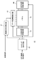
- FIG. 4 is a circuit block diagram of plasma display device 40 in accordance with the first exemplary embodiment of the present invention.
- the plasma display device 40 includes a panel 10 and a drive circuit that drives the panel 10.
- the drive circuit includes an image signal processing circuit 41, a data electrode drive circuit 42, a scan electrode drive circuit 43, a sustain electrode drive circuit 44, a timing generation circuit 45, and a power supply circuit (not shown) that supplies necessary power to each circuit block. It has.
- the image signal processing circuit 41 assigns a gradation value to each discharge cell based on the input image signal. Then, the gradation value is converted into image data indicating light emission / non-light emission for each subfield.
- the input image signal sig when the input image signal sig includes an R signal, a G signal, and a B signal, R, G, and B gradation values (in one field) are assigned to each discharge cell based on the R signal, the G signal, and the B signal. Assigned gradation value).
- the input image signal sig when the input image signal sig includes a luminance signal (Y signal) and a saturation signal (C signal, RY signal and BY signal, or u signal and v signal), the luminance signal and R, G, and B signals are calculated based on the saturation signal, and thereafter, R, G, and B gradation values are assigned to the respective discharge cells. Then, the R, G, and B gradation values assigned to each discharge cell are converted into image data indicating light emission / non-light emission for each subfield.
- the timing generation circuit 45 generates various timing signals for controlling the operation of each circuit block based on the horizontal synchronization signal and the vertical synchronization signal. Then, the generated timing signal is supplied to each circuit block (image signal processing circuit 41, data electrode drive circuit 42, scan electrode drive circuit 43, sustain electrode drive circuit 44, etc.).
- Scan electrode drive circuit 43 has an initialization waveform generation circuit, a sustain pulse generation circuit, and a scan pulse generation circuit (not shown).
- the initialization waveform generating circuit generates an initialization waveform to be applied to scan electrode SC1 through scan electrode SCn during the initialization period.
- the sustain pulse generation circuit generates a sustain pulse to be applied to scan electrode SC1 through scan electrode SCn during the sustain period.
- the scan pulse generating circuit includes a plurality of scan electrode driving ICs (scan ICs), and generates scan pulses to be applied to scan electrode SC1 through scan electrode SCn in the address period.
- Scan electrode driving circuit 43 drives scan electrode SC1 through scan electrode SCn based on the timing signal supplied from timing generation circuit 45, respectively.
- the data electrode drive circuit 42 converts the data for each subfield constituting the image data into address pulses corresponding to the data electrodes D1 to Dm. Then, based on the timing signal supplied from the timing generation circuit 45, an address pulse is applied to each of the data electrodes D1 to Dm.
- Sustain electrode drive circuit 44 includes a sustain pulse generation circuit and a circuit for generating voltage Ve (not shown), and drives sustain electrode SU1 through sustain electrode SUn based on the timing signal supplied from timing generation circuit 45.
- FIG. 5 is a circuit diagram schematically showing a configuration of scan electrode drive circuit 43 of plasma display device 40 in accordance with the first exemplary embodiment of the present invention.
- the scan electrode drive circuit 43 includes a sustain pulse generation circuit 50, a ramp waveform voltage generation circuit 60, and a scan pulse generation circuit 70. Each circuit block operates based on the timing signal supplied from the timing generation circuit 45, but details of the timing signal path are omitted in FIG.
- the voltage input to the scan pulse generation circuit 70 is referred to as “reference potential A”.
- Sustain pulse generation circuit 50 includes power recovery circuit 51, switching element Q55, switching element Q56, and switching element Q59.
- the power recovery circuit 51 includes a power recovery capacitor, a plurality of switching elements, a plurality of backflow prevention diodes, and a plurality of resonance inductors.
- the power recovery circuit 51 recovers the power stored in the panel 10 from the panel 10 through LC resonance between the interelectrode capacitance of the panel 10 and the inductor, and stores it in the capacitor. Then, the recovered power is LC-resonated between the interelectrode capacitance of the panel 10 and the inductor, supplied again from the capacitor to the panel 10, and reused as power for driving the scan electrodes SC1 to SCn.
- Switching element Q55 clamps scan electrode SC1 through scan electrode SCn to voltage Vs
- switching element Q56 clamps scan electrode SC1 through scan electrode SCn to voltage 0 (V).
- the switching element Q59 is a separation switch, and prevents a current from flowing back through a parasitic diode or the like of the switching element constituting the scan electrode driving circuit 43.
- sustain pulse generating circuit 50 generates a sustain pulse of voltage Vs applied to scan electrode SC1 through scan electrode SCn.
- Scan pulse generation circuit 70 sequentially applies scan pulses to scan electrode SC1 through scan electrode SCn at the timing shown in FIG. Scan pulse generation circuit 70 outputs the output voltage of sustain pulse generation circuit 50 as it is during the sustain period. That is, the reference potential A is output to scan electrode SC1 through scan electrode SCn.
- the ramp waveform voltage generation circuit 60 includes a Miller integration circuit 61, a Miller integration circuit 62, and a Miller integration circuit 63, and generates the ramp waveform voltage shown in FIG.
- Miller integrating circuit 61 includes transistor Q61, capacitor C61, and resistor R61. Then, by applying a constant voltage to the input terminal IN61 (giving a constant voltage difference between two circles shown as the input terminal IN61), an upward ramp waveform voltage that gradually increases toward the voltage Vt is obtained. appear.
- the voltage Vi2 is set to be equal to a voltage obtained by superimposing the voltage Vp on the voltage Vt. That is, when Miller integrating circuit 61 is operated, switching element Q72 and switching elements Q71L1 to Q71Ln are turned off, switching elements Q71H1 to switching element Q71Hn are turned on, and the upward slope generated in Miller integrating circuit 61 is generated. A voltage Vp of the power supply E71 is superimposed on the waveform voltage to generate an upslope waveform voltage having a forced initialization waveform.
- Miller integrating circuit 62 includes transistor Q62, capacitor C62, resistor R62, and diode Di62 for preventing backflow. Then, by applying a constant voltage to the input terminal IN62 (giving a constant voltage difference between two circles shown as the input terminal IN62), an upward ramp waveform voltage that gradually increases toward the voltage Vr1 is obtained. appear.
- Miller integrating circuit 63 includes transistor Q63, capacitor C63, and resistor R63. Then, by applying a constant voltage to the input terminal IN63 (giving a constant voltage difference between the two circles shown as the input terminal IN63), a downward ramp waveform voltage that gently falls toward the voltage Vi4 is obtained. appear.
- the switching element Q69 is a separation switch, and prevents a current from flowing back through a parasitic diode or the like of the switching element constituting the scan electrode driving circuit 43.
- switching elements and transistors can be configured using generally known semiconductor elements such as MOSFETs and IGBTs. These switching elements and transistors are controlled by timing signals corresponding to the respective switching elements and transistors generated by the timing generation circuit 45.
- the voltage Vi1 is equal to the voltage Vp
- the voltage Vi2 is equal to the voltage (Vt + Vp)
- the voltage Vi3 is equal to the voltage Vs
- the voltage Vc is equal to the voltage (Va + Vp). It shall be equal.
- these voltages are not limited to the above-described numerical values, and are desirably set as appropriate according to the characteristics of the panel 10 and the specifications of the plasma display device.
- FIG. 6 is a timing chart for explaining the operation of the driving circuit of the plasma display device 40 according to the first embodiment of the present invention.
- the scan electrode 22 to which the forced initialization waveform is applied is the scan electrode SC1
- the scan electrode 22 to which the selective initialization waveform is applied is the scan electrode SC2.
- the switching element corresponding to the scan electrode SC1 is referred to as a switching element Q71H1
- the switching element corresponding to the scan electrode SC1 is referred to as a switching element Q71H1.
- the switching element corresponding to scan electrode SC1 is referred to as switching element Q71L1
- the switching element corresponding to scan electrode SC1 is referred to as switching element Q71L1.
- the waveform shape of the rising ramp waveform voltage having the maximum voltage as the voltage Vr2 is different from the waveform shape of the rising ramp waveform voltage having the maximum voltage as the voltage Vr2 shown in FIG.
- the same effect as described above can be obtained with any upward ramp waveform voltage.
- FIG. 6 shows an example of generating an upslope waveform voltage that can achieve the same effect as described above even in such a case.
- the switching element Q56 of the scan electrode drive circuit 43 is turned on to apply the voltage 0 (V) to the scan electrode SC1 and the scan electrode SC1.
- switching element Q56 is turned off, and switching element Q71L1 is turned off, switching element Q71H1 is turned on, and voltage Vp is applied to scan electrode SC1 to which a forced initialization waveform is applied.
- the voltage 0 (V) is kept applied to the scan electrode SC2 to which the selective initialization waveform is applied without performing the forced initialization operation.
- a constant voltage is applied to the input terminal IN61 of the Miller integrating circuit 61, and the voltage of the reference potential A is gradually raised to the voltage Vt. Since a voltage obtained by superimposing the voltage Vp on the reference potential A is applied to the scan electrode SC1 to which the forced initializing waveform is applied, an ascending waveform that gently rises from the voltage Vp to the voltage (Vt + Vp). A voltage can be applied.
- the switching element Q71H1 of the scan electrode driving circuit 43 is turned off, the switching element Q71L1 is turned on, the switching element Q55 and the switching element Q59 are turned on, and the scan electrode A voltage Vs is applied to SC1 and scan electrode SC2.
- the switching element Q69 is turned off and a constant voltage is applied to the input terminal IN63 of the Miller integrating circuit 63 to operate the Miller integrating circuit 63, so that the scanning electrode SC1 and the scanning electrode SC2 are gradually applied from the voltage Vs to the voltage Vi4. A falling ramp waveform voltage is applied.
- the transistor Q63 of the Miller integrating circuit 63 of the scan electrode driving circuit 43 is turned off, the switching element Q72 is turned on, and the voltage of the reference potential A is set to the voltage Va. Then, switching element Q71L1 and switching element Q71L2 are turned off, switching element Q71H1 and switching element Q71H2 are turned on, and voltage (Va + Vp), that is, voltage Vc is applied to scan electrode SC1 and scan electrode SC2.
- switching element Q71H1 is turned off, switching element Q71L1 is turned on, and a scan pulse that is displaced from voltage Vc to voltage Va is applied to scan electrode SC1.
- the switching element Q71H1 is turned on, the switching element Q71L1 is turned off, and the voltage applied to the scan electrode SC1 is returned to the voltage Vc. In this way, a scan pulse is applied to scan electrode SC1.
- switching element Q71H2 is turned off, switching element Q71L2 is turned on, and a scan pulse that is displaced from voltage Vc to voltage Va is applied to scan electrode SC2.
- the switching element Q71H2 is turned on, the switching element Q71L2 is turned off, and the voltage applied to the scan electrode SC2 is returned to the voltage Vc. In this way, a scan pulse is applied to scan electrode SC2.
- scan pulses are sequentially applied to the scan electrode 22 until the scan electrode SCn is reached.
- switching element Q72, switching element Q71H1, and switching element Q71H2 are turned off, and switching element Q56, switching element Q69, switching element Q71L1, and switching element Q71L2 are turned on, respectively, and voltage 0 ( V) is applied.
- the writing period ends.
- the sustain pulse generation circuit 50 of the scan electrode driving circuit 43 is used to apply the number of sustain pulses corresponding to the luminance weight to scan electrode SC1 to scan electrode SCn.
- the switching element Q56 of the scan electrode drive circuit 43 is turned off.
- a constant voltage is applied to input terminal IN62 of Miller integrating circuit 62 to operate Miller integrating circuit 62, and an upward ramp waveform voltage that gradually rises to voltage Vr1 is applied to scan electrode SC1 through scan electrode SCn.
- the switching element Q71L1 to the switching element Q71Ln of the scan electrode driving circuit 43 are turned on, and the switching element Q71H1 to the switching element Q71Hn are kept off, and the input terminal IN63 of the Miller integrating circuit 63 is constant. Apply a voltage of. Miller integrating circuit 63 is thus operated, and a downward ramp waveform voltage that gently falls to voltage Vi4 is applied to scan electrode SC1 through scan electrode SCn.
- the sustain pulse generation circuit 50 of the scan electrode driving circuit 43 is used to apply the number of sustain pulses corresponding to the luminance weight to the scan electrodes SC1 to SCn.
- the switching element Q56 of the scan electrode drive circuit 43 is turned off.
- a constant voltage is applied to input terminal IN62 of Miller integrating circuit 62 to operate Miller integrating circuit 62, and an upward ramp waveform voltage that gradually rises to voltage Vr1 is applied to scan electrode SC1 through scan electrode SCn.
- switching element Q56 is turned on to apply voltage 0 (V) to scan electrode SC1 through scan electrode SCn. Thereafter, switching element Q56 is turned off.
- switching element Q71L1 to switching element Q71Ln are turned off, switching element Q71H1 to switching element Q71Hn are turned on, and voltage Vp is applied to scan electrode SC1 to scan electrode SCn.
- an upward ramp waveform voltage that rises to a voltage Vr2 higher than the voltage Vr1 is applied to scan electrode SC1 through scan electrode SCn.
- switching element Q71H1 to switching element Q71Hn are turned off, and switching element Q71L1 to switching element Q71Ln are turned on.
- the drive voltage waveforms shown in FIG. 3 are generated using data electrode drive circuit 42, scan electrode drive circuit 43, and sustain electrode drive circuit 44, and data electrodes D1 to D Dm is applied to each of scan electrode SC1 through scan electrode SCn and sustain electrode SU1 through sustain electrode SUn.
- the number of sustain pulses corresponding to a predetermined luminance weight is generated and applied alternately to the scan electrode 22 and the sustain electrode 23.
- sustain period Ts1 of subfields other than the final subfield in this embodiment, each subfield from subfield SF1 to subfield SF9
- the voltage rises to voltage Vr1.
- An upward ramp waveform voltage is generated and applied to the scan electrode 22.
- each discharge cell performs a forced initialization operation only once in a plurality of consecutive fields (for example, two consecutive fields in this embodiment).
- the frequency of the forced initialization operation is reduced, and the light emission not related to the gradation display is reduced. It is possible to reduce black luminance in the display image and display an image with high contrast.
- the uplink generated due to the erasing discharge is generated.
- the maximum voltage of the ramp waveform voltage is set to voltage Vr2, and the ramp waveform voltage generated for erasing discharge in the sustain period of the other subfield (in this embodiment, each subfield from subfield SF1 to subfield SF9) The maximum voltage is set to voltage Vr1. Then, the voltage Vr2 is set to a voltage higher than the voltage Vr1.
- the address discharge can be stably generated in the discharge cell that performs the selective initializing operation in the initializing period Ti1 of the subfield SF1 that is the specific cell initializing subfield. Can do.
- one field is composed of 10 subfields (subfield SF1 to subfield SF10), and the luminance weight increases in each subfield as the subfield occurs later in time.
- the luminance weight is set. Therefore, if a plurality of subfields that are temporally continuous so that the luminance weight becomes larger as a subfield that occurs later in time is defined as one subfield group, in this embodiment, one field is subfield SF1.
- subfield SF10 can be regarded as being composed of one subfield group consisting of ten subfields. Therefore, it can be said that subfield SF10 is the last subfield of one subfield group.
- the present invention is not limited to this configuration.
- the present invention is a subfield configuration in which a subfield with a small luminance weight is generated after a subfield with a large luminance weight is continuously generated and an initialization discharge is not generated in the subfield with the small luminance weight. With the same configuration as described above, the same effect as described above can be obtained.
- such a subfield configuration includes, for example, a subdevice designed to suppress flicker when an image is displayed on the panel 10 using a PAL image signal.
- a subdevice designed to suppress flicker when an image is displayed on the panel 10 using a PAL image signal.
- Embodiment 1 an example in which the configuration shown in Embodiment 1 is applied to a subfield configuration designed to suppress flicker when an image is displayed on the panel 10 using a PAL image signal will be described.
- the configuration of the plasma display device is the same as the configuration of the plasma display device 40 shown in the first embodiment, and a description thereof will be omitted.
- the subfield configuration is different from the subfield configuration shown in the first embodiment.
- one field is composed of 14 subfields (subfield SF1 to subfield SF14), and each subfield is (1, 2, 4, 8, 20, 32, 56, 4, 12). , 16, 16, 20, 32, 32) will be described.
- the luminance weight of the plurality of subfields constituting one field increases from the subfield SF1 to the subfield SF7, and the luminance weight temporarily decreases from the subfield SF7 to the subfield SF8.
- the luminance weight increases again from subfield SF8 to subfield SF14.
- one field is subfield SF1.
- a subfield group consisting of seven subfields and a subfield group consisting of seven subfields from subfield SF8 to subfield SF14 be able to.
- Such a sub-field configuration has a flicker (image flicker) when an image signal with a low field frequency (number of fields generated per second) is displayed on the panel 10, such as a PAL image signal. It is effective in suppressing the occurrence.
- FIG. 7 is a diagram showing drive voltage waveforms applied to each electrode of the panel used in the plasma display device in accordance with the second exemplary embodiment of the present invention.
- FIG. 7 shows scan electrode SC1 that performs the address operation first in the address period, scan electrode SC2 that performs the address operation second in the address period, sustain electrode SU1 to sustain electrode SUn, and data electrode D1 to data electrode Dm.
- the drive voltage waveform applied to is shown.
- FIG. 7 shows the drive voltage waveforms of two subfields having different waveform shapes of the drive voltages applied to scan electrode SC1 through scan electrode SCn during the initialization period.
- These two subfields are a subfield SF1 that is an all-cell initializing subfield and a subfield after the subfield SF2 that is a selective initializing subfield.
- the all-cell initializing subfield refers to initializing discharge cells in all the discharge cells in the image display area of the panel 10 by applying a forced initializing waveform to all the scan electrodes SC1 to SCn in the initializing period. A subfield that occurs.
- the initialization period of the all-cell initialization subfield is also referred to as “all-cell initialization period”.
- the drive voltage waveform in the subfield after subfield SF3 is substantially the same as the drive voltage waveform in subfield SF2 except that the number of sustain pulses generated in the sustain period is different.
- the waveform shape of the rising ramp waveform voltage for generating the erasing discharge is different from the rising ramp waveform voltage for generating the erasing discharge in the other subfields.
- subfield SF1 which is an all-cell initialization subfield
- the forced initializing waveform shown in the first embodiment is applied to all the scan electrodes SC1 to SCn.
- a voltage of 0 (V) is applied to the data electrode D1 to the data electrode Dm and the sustain electrode SU1 to the sustain electrode SUn.
- Voltage Vi1 is applied to scan electrode SC1 through scan electrode SCn.
- Voltage Vi1 is set to a voltage lower than the discharge start voltage with respect to sustain electrode SU1 through sustain electrode SUn.
- an upward ramp waveform voltage that gently rises from voltage Vi1 to voltage Vi2 is applied to scan electrode SC1 through scan electrode SCn.
- While the rising ramp waveform voltage is rising, between scan electrode SC1 through scan electrode SCn and sustain electrode SU1 through sustain electrode SUn, and between scan electrode SC1 through scan electrode SCn and data electrode D1 through data electrode Dm.
- a weak initializing discharge is continuously generated.
- Negative wall voltage is accumulated on scan electrode SC1 through scan electrode SCn
- positive wall voltage is accumulated on data electrode D1 through data electrode Dm and sustain electrode SU1 through sustain electrode SUn.
- priming particles that help generate subsequent discharge are also generated.
- positive voltage Ve is applied to sustain electrode SU1 through sustain electrode SUn, and voltage 0 (V) is applied as the first voltage to data electrode D1 through data electrode Dm.
- a downward ramp waveform voltage that gently decreases from voltage Vi3 toward negative voltage Vi4 is applied to scan electrode SC1 through scan electrode SCn.
- the voltage Vi3 is set to a voltage lower than the discharge start voltage with respect to the sustain electrodes SU1 to SUn, and the voltage Vi4 is set to a voltage exceeding the discharge start voltage.
- the negative wall voltage on scan electrode SC1 through scan electrode SCn and the positive wall voltage on sustain electrode SU1 through sustain electrode SUn are weakened, and the positive wall voltage on data electrode D1 through data electrode Dm is used for the write operation. It is adjusted to a suitable value.
- priming particles that help generate subsequent discharge are also generated.
- the same drive voltage waveform as that in the address period Tw shown in the first embodiment is applied to each electrode. That is, a scan pulse is sequentially applied to scan electrode SC1 through scan electrode SCn, and an address pulse of voltage Vd is applied to data electrode Dk corresponding to a discharge cell to emit light. Thus, an address discharge is generated in the discharge cell to emit light, and wall charges necessary for the subsequent sustain discharge are formed.
- a drive voltage waveform similar to that in the sustain period Ts1 described in the first embodiment is applied to each electrode. That is, the number of sustain pulses corresponding to the luminance weight is generated and applied alternately to scan electrode SC1 through scan electrode SCn and sustain electrode SU1 through sustain electrode SUn, and the luminance weight is applied to the discharge cells that have caused the address discharge. The number of times of sustain discharge is generated.
- the selective initialization waveform shown in the first embodiment is applied to all the scan electrodes SC1 to SCn.
- the voltage 0 (V) is applied to the data electrodes D1 to Dm, and the voltage Ve is applied to the sustain electrodes SU1 to SUn.
- Scan electrode SC1 through scan electrode SCn gradually decrease from voltage Vi3 ′ (eg, voltage 0 (V), which is the base potential), which is less than the discharge start voltage, to negative voltage Vi4 that exceeds the discharge start voltage. Apply a downward ramp waveform voltage.
- the initialization discharge does not occur, and the wall charge at the end of the immediately preceding subfield initialization period is maintained. In this way, the initialization operation in the subfield SF2 is completed.
- the initializing operation in subfield SF2 is a selective initializing operation in which initializing discharge is generated only in the discharge cells in which the address discharge is generated in the address period of the immediately preceding subfield and the sustain discharge is generated in the sustain period.
- the same drive voltage waveform as that in the address period and the sustain period of the subfield SF1 is applied to each electrode, except for the number of sustain pulses.
- each subfield from subfield SF3 to subfield SF6 the drive voltage waveform similar to that in subfield SF2 is applied to each electrode except for the number of sustain pulses generated in sustain period Ts1.
- the same drive voltage waveform as that of the subfield SF2 is applied to each electrode. Further, in the sustain period Ts2 of the subfield SF7, a sustain pulse similar to the sustain pulse in the sustain period Ts1 of the subfield SF2 is alternately applied to the display electrode pair 24, except for the number of sustain pulses generated.
- the rising ramp waveform voltage for the erasing discharge generated in the sustain period Ts2 of the subfield SF7 has a waveform shape different from the rising ramp waveform voltage for the erasing discharge generated in the sustaining period Ts1 of the subfield SF2.
- sustain period Ts2 of subfield SF7 after the generation of the last sustain pulse in sustain period Ts2, an upward ramp waveform voltage that gradually rises from voltage 0 (V) to voltage Vr2 is generated and applied to scan electrode SC1 through scan electrode SCn. Apply. Then, the voltage Vr2 is set to a voltage higher than the voltage Vr1.
- each subfield from subfield SF8 to subfield SF14, which is the second subfield group the same drive voltage waveform as in subfield SF2 is applied to each electrode except for the number of sustain pulses generated in sustain period Ts1. To do.
- the selective initialization operation is performed in the initialization period Ti1 of the subfield SF8 which is the first subfield of the second subfield group.
- the luminance weight is set in each subfield so that the luminance weight increases as the subfield occurs later in time.
- the subfield immediately before the subfield SF8 is the last subfield of the first subfield group, and is the subfield having the largest luminance weight in the subfield group.
- the probability that subfield SF6 and subfield SF7 having relatively large luminance weights emit light is relatively low, and subfield SF8 having a small luminance weight has The probability of emitting light is relatively high. Therefore, there is a relatively high probability that subfield SF6 and subfield SF7 are non-light emitting subfields, and subfield SF8 is a light emitting subfield.
- the initializing discharge does not occur in the initializing period Ti2 of the subfield SF8 that is the selective initializing subfield, and for the reason described above. There is a possibility that the address discharge cannot be generated.
- the voltage Vr2 that is the maximum voltage of the rising ramp waveform voltage that is generated is set to a voltage that is higher than the voltage Vr1 that is the maximum voltage of the rising ramp waveform voltage for the erasing discharge that occurs in the subfield having a relatively small luminance weight.
- the above-described subfield having a relatively small luminance weight and performing the selective initialization operation in the initialization period has the luminance weight “4”, and performs the selective initialization operation in the initialization period.
- the subfield having a relatively large luminance weight is the subfield SF7 having the luminance weight “56”.
- the sustain period of the subfield immediately before the second subfield group that is, the last subfield of the first subfield group (subfield SF7 in the present embodiment).
- the maximum voltage of the rising ramp waveform voltage generated for erasing discharge is defined as voltage Vr2.
- Voltage Vr2 is generated due to erasing discharge in the sustain period of other subfields (in this embodiment, subfields SF1 to SF6 and subfield SF8 to subfield SF14).
- a voltage higher than the voltage Vr1, which is the maximum voltage of the ramp waveform voltage, is set.
- the subfield SF6 and the subfield SF7 continuously become non-light-emitting subfields, and the discharge cells that may cause a write failure in the subsequent subfield SF8 remain on the data electrode 32.
- the negative wall voltage is inverted, and the occurrence of write failure can be prevented in the subsequent subfield SF8.
- the configuration for generating the rising ramp waveform voltage having the maximum voltage Vr2 in the last subfield SF7 of the first subfield group has been described.
- the present invention is not limited to this configuration.
- an upward ramp waveform voltage whose maximum voltage is the voltage Vr2 may be generated. This is particularly effective in a subfield configuration in which the subfield SF1 is a specific cell initialization subfield because the forced initialization operation is performed only once in a plurality of consecutive fields.
- the number of subfields constituting one field, subfields to be forced initialization subfields, luminance weights of each subfield, and the like are not limited to the above-described numerical values. Moreover, the structure which switches a subfield structure based on an image signal etc. may be sufficient.
- the driving voltage waveforms shown in FIGS. 3, 6, and 7 are merely examples in the embodiment of the present invention, and the present invention is not limited to these driving voltage waveforms.
- the configuration of the drive circuit shown in FIGS. 4 and 5 is merely an example in the embodiment of the present invention, and the present invention is not limited to these circuit configurations.
- each circuit block shown in the embodiment of the present invention may be configured as an electric circuit that performs each operation shown in the embodiment, or a microcomputer that is programmed to perform the same operation. May be used.
- the number of subfields constituting one field is not limited to the above number.
- the number of gradations that can be displayed on the panel 10 can be further increased.
- the time required for driving panel 10 can be shortened by reducing the number of subfields.
- one pixel is constituted by discharge cells of three colors of red, green, and blue.
- a panel in which one pixel is constituted by discharge cells of four colors or more has been described.
- the specific numerical values shown in the embodiment of the present invention are set based on the characteristics of the panel 10 having a screen size of 50 inches and the number of display electrode pairs 24 of 1024. It is just an example.
- the present invention is not limited to these numerical values, and each numerical value is desirably set optimally in accordance with panel specifications, panel characteristics, plasma display device specifications, and the like. Each of these numerical values is allowed to vary within a range where the above-described effect can be obtained.
- the number of subfields constituting one field, the luminance weight of each subfield, etc. are not limited to the values shown in the embodiment of the present invention, and the subfield configuration is based on the image signal or the like. The structure to switch may be sufficient.
- the present invention can perform a stable writing operation even when driving a high-definition large-screen panel, and can display a high-quality image on the panel. It is useful as a plasma display device.
- SYMBOLS 10 Panel 21 Front substrate 22 Scan electrode 23 Sustain electrode 24 Display electrode pair 25,33 Dielectric layer 26 Protective layer 31 Back substrate 32 Data electrode 34 Partition 35 Phosphor layer 40 Plasma display device 41 Image signal processing circuit 42 Data electrode drive circuit 43 Scan electrode drive circuit 44 Sustain electrode drive circuit 45 Timing generation circuit 50 Sustain pulse generation circuit 51 Power recovery circuit 60 Ramp waveform voltage generation circuit 61, 62, 63 Miller integration circuit 70 Scan pulse generation circuit Di62 Diodes Q55, Q56, Q59, Q69, Q72, Q71H1 to Q71Hn, Q71L1 to Q71Ln Switching elements C61, C62, C63 Capacitors R61, R62, R63 Resistors Q61, Q62, Q63 Transistors IN61, IN62, N63 input terminal E71 power Ti1, Ti2 initialization period Tw write period Ts1, Ts2 sustain period
Landscapes
- Engineering & Computer Science (AREA)
- Physics & Mathematics (AREA)
- Power Engineering (AREA)
- Plasma & Fusion (AREA)
- Computer Hardware Design (AREA)
- General Physics & Mathematics (AREA)
- Theoretical Computer Science (AREA)
- Control Of Indicators Other Than Cathode Ray Tubes (AREA)
- Control Of Gas Discharge Display Tubes (AREA)
Abstract
Une opération d'écriture stable est effectuée pendant la commande d'un panneau d'affichage à plasma à haute définition et grand écran. Il est proposé, par conséquent, un procédé de commande pour commander un panneau d'affichage à plasma dans lequel un champ unique est composé de sous-champs ayant une période d'initialisation pour effectuer une opération d'initialisation sélective au cours de laquelle une tension à forme d'onde inclinée vers le bas qui diminue vers une tension négative est appliquée à une électrode de balayage, une période d'écriture et une période d'entretien pendant laquelle le nombre d'impulsions d'entretien qui correspond à des coefficients de pondération de luminance est appliqué à une paire d'électrodes d'affichage, une forme d'onde inclinée vers le haut pour générer une décharge d'effacement dans une cellule de décharge étant appliquée à l'électrode de balayage après que l'impulsion d'entretien finale a été générée dans la période d'entretien. Dans un sous-champ ayant un coefficient de pondération de luminance relativement élevé généré immédiatement avant un sous-champ dans lequel le coefficient de pondération de luminance est relativement faible et dans lequel l'opération d'initialisation sélective est effectuée dans la période d'initialisation, la tension maximum de la tension à forme d'onde inclinée vers le haut est fixée à une tension élevée supérieure à la tension maximum de la tension à forme d'onde inclinée vers le haut générée dans le sous-champ ayant le coefficient de pondération de luminance relativement faible.
Priority Applications (2)
| Application Number | Priority Date | Filing Date | Title |
|---|---|---|---|
| CN2012800037946A CN103229226A (zh) | 2011-01-28 | 2012-01-26 | 等离子显示面板的驱动方法以及等离子显示装置 |
| JP2012554694A JPWO2012102043A1 (ja) | 2011-01-28 | 2012-01-26 | プラズマディスプレイパネルの駆動方法およびプラズマディスプレイ装置 |
Applications Claiming Priority (2)
| Application Number | Priority Date | Filing Date | Title |
|---|---|---|---|
| JP2011-016042 | 2011-01-28 | ||
| JP2011016042 | 2011-01-28 |
Publications (1)
| Publication Number | Publication Date |
|---|---|
| WO2012102043A1 true WO2012102043A1 (fr) | 2012-08-02 |
Family
ID=46580618
Family Applications (1)
| Application Number | Title | Priority Date | Filing Date |
|---|---|---|---|
| PCT/JP2012/000484 Ceased WO2012102043A1 (fr) | 2011-01-28 | 2012-01-26 | Procédé de commande de panneau d'affichage à plasma et dispositif d'affichage à plasma |
Country Status (3)
| Country | Link |
|---|---|
| JP (1) | JPWO2012102043A1 (fr) |
| CN (1) | CN103229226A (fr) |
| WO (1) | WO2012102043A1 (fr) |
Citations (10)
| Publication number | Priority date | Publication date | Assignee | Title |
|---|---|---|---|---|
| JPH11242459A (ja) * | 1998-02-25 | 1999-09-07 | Nec Corp | プラズマディスプレイパネルの駆動方法 |
| JP2000172224A (ja) * | 1998-12-08 | 2000-06-23 | Hitachi Ltd | プラズマディスプレイパネルの駆動方法及びプラズマディスプレイ |
| JP2003005700A (ja) * | 2001-06-20 | 2003-01-08 | Matsushita Electric Ind Co Ltd | プラズマディスプレイ表示装置 |
| JP2003005704A (ja) * | 2001-06-25 | 2003-01-08 | Matsushita Electric Ind Co Ltd | プラズマディスプレイの駆動方法 |
| JP2003050562A (ja) * | 2001-08-08 | 2003-02-21 | Fujitsu Hitachi Plasma Display Ltd | プラズマディスプレイ装置の駆動方法 |
| JP2003140609A (ja) * | 2001-10-31 | 2003-05-16 | Matsushita Electric Ind Co Ltd | プラズマディスプレイの駆動方法 |
| JP2005148594A (ja) * | 2003-11-19 | 2005-06-09 | Pioneer Plasma Display Corp | プラズマディスプレイパネルの駆動方法 |
| JP2006308625A (ja) * | 2005-04-26 | 2006-11-09 | Matsushita Electric Ind Co Ltd | プラズマディスプレイ装置 |
| JP2010107547A (ja) * | 2008-10-28 | 2010-05-13 | Panasonic Corp | プラズマディスプレイパネルの駆動方法およびプラズマディスプレイ装置 |
| JP2010249914A (ja) * | 2009-04-13 | 2010-11-04 | Panasonic Corp | プラズマディスプレイパネルの駆動方法およびプラズマディスプレイ装置 |
Family Cites Families (8)
| Publication number | Priority date | Publication date | Assignee | Title |
|---|---|---|---|---|
| EP1202241B1 (fr) * | 1998-09-04 | 2007-09-12 | Matsushita Electric Industrial Co., Ltd. | Procédé de commande d'écran au plasma et appareil à écran au plasma capable d'afficher des images de haute qualité à haut rendement lumineux |
| KR100697891B1 (ko) * | 2000-09-04 | 2007-03-21 | 오리온피디피주식회사 | 플라즈마 디스플레이 패널의 구동방법 |
| WO2002101707A1 (fr) * | 2001-06-12 | 2002-12-19 | Matsushita Electric Industrial Co., Ltd. | Ecran a plasma et son procede d'attaque |
| KR100563464B1 (ko) * | 2003-11-03 | 2006-03-23 | 엘지전자 주식회사 | 플라즈마 디스플레이 패널의 구동방법 |
| KR100499101B1 (ko) * | 2003-11-04 | 2005-07-01 | 엘지전자 주식회사 | 플라즈마 디스플레이 패널의 구동방법 및 장치 |
| KR20070075205A (ko) * | 2006-01-12 | 2007-07-18 | 엘지전자 주식회사 | 플라즈마 디스플레이 장치 |
| WO2007099903A1 (fr) * | 2006-02-28 | 2007-09-07 | Matsushita Electric Industrial Co., Ltd. | Procede d'entrainement de panneau d'affichage plasma et dispositif d'affichage plasma |
| CN101055692A (zh) * | 2006-04-12 | 2007-10-17 | 乐金电子(南京)等离子有限公司 | 等离子显示器的驱动方法 |
-
2012
- 2012-01-26 WO PCT/JP2012/000484 patent/WO2012102043A1/fr not_active Ceased
- 2012-01-26 CN CN2012800037946A patent/CN103229226A/zh active Pending
- 2012-01-26 JP JP2012554694A patent/JPWO2012102043A1/ja active Pending
Patent Citations (10)
| Publication number | Priority date | Publication date | Assignee | Title |
|---|---|---|---|---|
| JPH11242459A (ja) * | 1998-02-25 | 1999-09-07 | Nec Corp | プラズマディスプレイパネルの駆動方法 |
| JP2000172224A (ja) * | 1998-12-08 | 2000-06-23 | Hitachi Ltd | プラズマディスプレイパネルの駆動方法及びプラズマディスプレイ |
| JP2003005700A (ja) * | 2001-06-20 | 2003-01-08 | Matsushita Electric Ind Co Ltd | プラズマディスプレイ表示装置 |
| JP2003005704A (ja) * | 2001-06-25 | 2003-01-08 | Matsushita Electric Ind Co Ltd | プラズマディスプレイの駆動方法 |
| JP2003050562A (ja) * | 2001-08-08 | 2003-02-21 | Fujitsu Hitachi Plasma Display Ltd | プラズマディスプレイ装置の駆動方法 |
| JP2003140609A (ja) * | 2001-10-31 | 2003-05-16 | Matsushita Electric Ind Co Ltd | プラズマディスプレイの駆動方法 |
| JP2005148594A (ja) * | 2003-11-19 | 2005-06-09 | Pioneer Plasma Display Corp | プラズマディスプレイパネルの駆動方法 |
| JP2006308625A (ja) * | 2005-04-26 | 2006-11-09 | Matsushita Electric Ind Co Ltd | プラズマディスプレイ装置 |
| JP2010107547A (ja) * | 2008-10-28 | 2010-05-13 | Panasonic Corp | プラズマディスプレイパネルの駆動方法およびプラズマディスプレイ装置 |
| JP2010249914A (ja) * | 2009-04-13 | 2010-11-04 | Panasonic Corp | プラズマディスプレイパネルの駆動方法およびプラズマディスプレイ装置 |
Also Published As
| Publication number | Publication date |
|---|---|
| JPWO2012102043A1 (ja) | 2014-06-30 |
| CN103229226A (zh) | 2013-07-31 |
Similar Documents
| Publication | Publication Date | Title |
|---|---|---|
| JP5104757B2 (ja) | プラズマディスプレイ装置およびプラズマディスプレイパネルの駆動方法 | |
| WO2010146827A1 (fr) | Procédé de commande pour panneau d'affichage à plasma, et dispositif d'affichage à plasma | |
| JP2010266651A (ja) | プラズマディスプレイパネルの駆動方法およびプラズマディスプレイ装置 | |
| JPWO2012090451A1 (ja) | プラズマディスプレイパネルの駆動方法およびプラズマディスプレイ装置 | |
| WO2012102043A1 (fr) | Procédé de commande de panneau d'affichage à plasma et dispositif d'affichage à plasma | |
| JP5263450B2 (ja) | プラズマディスプレイパネルの駆動方法およびプラズマディスプレイ装置 | |
| WO2012073516A1 (fr) | Procédé de pilotage de dispositif d'affichage à plasma et dispositif d'affichage à plasma | |
| JP2010266648A (ja) | プラズマディスプレイパネルの駆動方法およびプラズマディスプレイ装置 | |
| WO2011096220A1 (fr) | Dispositif d'affichage à plasma et procédé de pilotage d'un écran d'affichage à plasma | |
| WO2012017648A1 (fr) | Procédé d'excitation d'écran d'affichage à plasma et appareil d'affichage à plasma | |
| WO2010131466A1 (fr) | Procédé de commande de panneau d'affichage à plasma et dispositif d'affichage à plasma | |
| JP2010266652A (ja) | プラズマディスプレイパネルの駆動方法およびプラズマディスプレイ装置 | |
| WO2012102032A1 (fr) | Procédé de commande de panneau d'affichage à plasma et dispositif d'affichage à plasma | |
| JP2010175772A (ja) | プラズマディスプレイパネルの駆動方法 | |
| WO2012102031A1 (fr) | Procédé de commande de panneau d'affichage à plasma et appareil d'affichage à plasma | |
| WO2013046652A1 (fr) | Procédé de commande de panneau d'affichage à plasma et dispositif d'affichage à plasma | |
| WO2012017647A1 (fr) | Procédé d'excitation d'écran à plasma et appareil d'affichage à plasma | |
| WO2012102033A1 (fr) | Procédé de commande de panneau d'affichage à plasma et dispositif d'affichage à plasma | |
| WO2011148644A1 (fr) | Procédé d'attaque d'un panneau d'affichage à plasma et dispositif d'affichage à plasma | |
| JP2010266649A (ja) | プラズマディスプレイパネルの駆動方法およびプラズマディスプレイ装置 | |
| JP2013148762A (ja) | プラズマディスプレイパネルの駆動方法 | |
| JP2009251267A (ja) | プラズマディスプレイ装置およびプラズマディスプレイパネルの駆動方法 | |
| WO2011052219A1 (fr) | Procédé de commande de panneau d'affichage à plasma et dispositif d'affichage à plasma | |
| JP2010266650A (ja) | プラズマディスプレイパネルの駆動方法およびプラズマディスプレイ装置 | |
| WO2012035761A1 (fr) | Dispositif d'affichage au plasma et son procédé d'activation |
Legal Events
| Date | Code | Title | Description |
|---|---|---|---|
| 121 | Ep: the epo has been informed by wipo that ep was designated in this application |
Ref document number: 12739103 Country of ref document: EP Kind code of ref document: A1 |
|
| ENP | Entry into the national phase |
Ref document number: 2012554694 Country of ref document: JP Kind code of ref document: A |
|
| NENP | Non-entry into the national phase |
Ref country code: DE |
|
| 122 | Ep: pct application non-entry in european phase |
Ref document number: 12739103 Country of ref document: EP Kind code of ref document: A1 |