WO2012102232A1 - Circuit d'entraînement pour un moteur pas à pas, son circuit intégré et dispositif électronique le comprenant, et procédé de commande pour un circuit d'entraînement de moteur pas à pas - Google Patents
Circuit d'entraînement pour un moteur pas à pas, son circuit intégré et dispositif électronique le comprenant, et procédé de commande pour un circuit d'entraînement de moteur pas à pas Download PDFInfo
- Publication number
- WO2012102232A1 WO2012102232A1 PCT/JP2012/051325 JP2012051325W WO2012102232A1 WO 2012102232 A1 WO2012102232 A1 WO 2012102232A1 JP 2012051325 W JP2012051325 W JP 2012051325W WO 2012102232 A1 WO2012102232 A1 WO 2012102232A1
- Authority
- WO
- WIPO (PCT)
- Prior art keywords
- stepping motor
- drive circuit
- abnormality
- excitation current
- signal
- Prior art date
- Legal status (The legal status is an assumption and is not a legal conclusion. Google has not performed a legal analysis and makes no representation as to the accuracy of the status listed.)
- Ceased
Links
Images






Classifications
-
- H—ELECTRICITY
- H02—GENERATION; CONVERSION OR DISTRIBUTION OF ELECTRIC POWER
- H02P—CONTROL OR REGULATION OF ELECTRIC MOTORS, ELECTRIC GENERATORS OR DYNAMO-ELECTRIC CONVERTERS; CONTROLLING TRANSFORMERS, REACTORS OR CHOKE COILS
- H02P8/00—Arrangements for controlling dynamo-electric motors rotating step by step
- H02P8/34—Monitoring operation
-
- H—ELECTRICITY
- H02—GENERATION; CONVERSION OR DISTRIBUTION OF ELECTRIC POWER
- H02P—CONTROL OR REGULATION OF ELECTRIC MOTORS, ELECTRIC GENERATORS OR DYNAMO-ELECTRIC CONVERTERS; CONTROLLING TRANSFORMERS, REACTORS OR CHOKE COILS
- H02P8/00—Arrangements for controlling dynamo-electric motors rotating step by step
- H02P8/36—Protection against faults, e.g. against overheating or step-out; Indicating faults
- H02P8/38—Protection against faults, e.g. against overheating or step-out; Indicating faults the fault being step-out
-
- H—ELECTRICITY
- H02—GENERATION; CONVERSION OR DISTRIBUTION OF ELECTRIC POWER
- H02P—CONTROL OR REGULATION OF ELECTRIC MOTORS, ELECTRIC GENERATORS OR DYNAMO-ELECTRIC CONVERTERS; CONTROLLING TRANSFORMERS, REACTORS OR CHOKE COILS
- H02P8/00—Arrangements for controlling dynamo-electric motors rotating step by step
- H02P8/36—Protection against faults, e.g. against overheating or step-out; Indicating faults
-
- B—PERFORMING OPERATIONS; TRANSPORTING
- B41—PRINTING; LINING MACHINES; TYPEWRITERS; STAMPS
- B41J—TYPEWRITERS; SELECTIVE PRINTING MECHANISMS, i.e. MECHANISMS PRINTING OTHERWISE THAN FROM A FORME; CORRECTION OF TYPOGRAPHICAL ERRORS
- B41J19/00—Character- or line-spacing mechanisms
- B41J19/18—Character-spacing or back-spacing mechanisms; Carriage return or release devices therefor
- B41J19/20—Positive-feed character-spacing mechanisms
- B41J19/202—Drive control means for carriage movement
Definitions
- the present invention relates to a driving circuit for a stepping motor, an integrated circuit in which the driving circuit is integrated, an electronic apparatus including the integrated circuit, and a method for controlling the driving circuit for a stepping motor, and more specifically, an excitation current from the driving circuit to the stepping motor.
- the present invention relates to a technique for detecting an abnormality in a path that transmits a signal.
- stepping motors that realize smooth rotation without unevenness and enable low vibration and low noise are often used.
- a stepping motor is driven by applying excitation currents whose phases are shifted from each other by 90 ° to a two-phase excitation coil with a waveform close to a sine wave (that is, a pseudo sine wave).
- Patent Document 1 discloses a target voltage generation unit that generates a target voltage that indicates a target value of an excitation current based on a reference voltage that indicates an upper limit value of the excitation current, and based on the target voltage.
- An example of a stepping motor drive circuit including a current control unit for controlling the excitation current is disclosed.
- the drive circuit and the stepping motor are connected to each other by wiring.
- This wiring is connected by connection parts, such as a terminal or a connector, in a drive circuit and a stepping motor. Furthermore, in the middle part of the wiring, the wiring may be connected by a connector or the like.
- connection part of this wiring is loosened, poor contact, or the wiring is disconnected, the excitation current cannot be supplied appropriately from the drive circuit to the excitation coil. Can not be.
- Patent Document 1 Japanese Patent Laid-Open No. 2008-029145
- the present invention has been made to solve such problems, and an object thereof is to provide a stepping motor drive circuit capable of detecting an abnormality in wiring for supplying an excitation current to the stepping motor. That is.
- a driving circuit for a stepping motor includes a target voltage generating unit for generating a target voltage indicating a target value for an exciting current determined based on a reference voltage indicating an upper limit value of an exciting current flowing in the stepping motor, and a target A current control unit that controls the excitation current so that the value of the excitation current is maintained at a target value based on the voltage;
- the current control unit includes a comparison unit for comparing a signal corresponding to the excitation current with a predetermined threshold value.
- the drive circuit further includes an abnormality detection unit for detecting an abnormality in a path through which the excitation current is supplied from the drive circuit to the stepping motor based on an output signal from the comparison unit.
- the comparison unit compares a voltage corresponding to the excitation current with a target voltage as a threshold value.
- the abnormality detection unit detects an abnormality based on the output signal from the comparison unit and the control signal indicating the polarity of the excitation current.
- the stepping motor includes first and second exciting coils.
- the current control unit includes a first channel and a second channel for outputting an excitation current corresponding to each of the first and second excitation coils.
- the current control unit has an abnormality based on the state of the output signal of the other channel at a predetermined timing when the control signal for one of the first and second channels is in a predetermined state. Detect that.
- the current control unit sets the voltage corresponding to the excitation current for the other channel to the target value of the channel.
- the output signal indicates that it has not reached, it is detected that an abnormality has occurred.
- control signal is a pulse signal.
- the predetermined timing is determined based on the falling timing of the control signal.
- the target voltage generation unit generates the target voltage by dividing the reference voltage according to a ratio that changes stepwise from 0 to 1 of the target value with respect to the upper limit value.
- the drive circuit further includes a command generation unit that generates a signal indicating a ratio and a control signal based on information from outside the drive circuit.
- the abnormality detection unit is based on the number of times that the level of the signal corresponding to the excitation current reaches the threshold value within a predetermined period in a state where the excitation current can be output from the drive circuit to the stepping motor. To detect abnormalities.
- the threshold value is determined based on the target value.
- the abnormality detection unit counts the number of times based on the output signal from the comparison unit.
- the abnormality detection unit detects that an abnormality has occurred when the number of times falls below a predetermined reference number.
- the threshold value is determined based on a minimum current value that is different from the target value and that can drive the stepping motor.
- the abnormality detection unit counts the number of times based on the output signal from the comparison unit.
- the threshold value is set based on a value lower than the target value.
- the predetermined period is determined based on at least one of a start signal for the drive circuit, an enable signal for enabling the drive circuit, and a control signal indicating the polarity of the excitation current.
- the abnormality detection unit determines the abnormality in response to the abnormality being continuously detected a predetermined number of times.
- the abnormality detection unit outputs an abnormality signal based on the fact that the abnormality has been confirmed.
- An integrated circuit according to the present invention is obtained by integrating any one of the drive circuits described above.
- An electronic apparatus includes a stepping motor and any one of the drive circuits described above.
- the stepping motor drive circuit control method includes a step of generating a target voltage indicating a target value for an excitation current determined based on a reference voltage indicating an upper limit value of the excitation current flowing in the stepping motor, and a target voltage. Based on this, the step of controlling the exciting current so that the value of the exciting current is maintained at the target value, the step of comparing the signal corresponding to the exciting current with a predetermined threshold, and the output signal by the step of comparing And detecting an abnormality in a path through which an exciting current is supplied from the drive circuit to the stepping motor.
- the comparing step includes a step of comparing a voltage corresponding to the exciting current with a target voltage as a threshold value.
- the step of detecting the abnormality includes a step of detecting the abnormality based on the output signal and a control signal indicating the polarity of the excitation current.
- the method further includes a step of counting the number of times that the level of the signal corresponding to the excitation current reaches the threshold value within a predetermined period in a state where the excitation current can be output from the drive circuit to the stepping motor.
- the step of detecting the abnormality includes a step of detecting the abnormality based on the number of times.
- FIG. 1 is an overall block diagram of a motor drive system including a drive circuit for a stepping motor according to a first embodiment. It is an example of the time chart for demonstrating abnormality detection control in the case of full step mode. It is an example of the time chart for demonstrating abnormality detection control in the case of a half step mode. It is another example of the time chart for demonstrating abnormality detection control in the case of a half step mode.
- FIG. 3 is a functional block diagram for explaining abnormality detection control executed by an abnormality detection unit in the first embodiment. 5 is a flowchart for illustrating details of an abnormality detection control process executed by an abnormality detection unit in the first embodiment.
- FIG. 6 is an overall block diagram of a motor drive system including a drive circuit for a stepping motor according to a second embodiment.
- FIG. 10 is an overall block diagram of a motor drive system including a drive circuit for a stepping motor according to a third embodiment.
- 12 is a first time chart for illustrating abnormality detection control in the third embodiment.
- 10 is a second time chart for illustrating abnormality detection control in the third embodiment.
- it is a functional block diagram for demonstrating abnormality detection control performed by the abnormality detection part.
- 10 is a flowchart for explaining details of an abnormality detection control process executed by an abnormality detection unit in the third embodiment.
- FIG. 10 is an overall block diagram of a motor drive system including a drive circuit for a stepping motor according to a fourth embodiment.
- FIG. 10 is an overall block diagram of a motor drive system including a drive circuit for a stepping motor according to a fifth embodiment.
- 10 is a time chart for explaining abnormality detection control in a fifth embodiment.
- it is a flowchart for demonstrating the detail of the abnormality detection control process performed in an abnormality detection part.
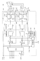
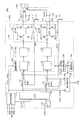
- FIG. 1 is an overall block diagram of a motor drive system 10 including a stepping motor drive circuit 100 according to the first embodiment.
- the motor drive system 10 is used as a drive unit of an electronic device such as a printer, a fax machine, a scanner, or a camera, for example.
- stepping motor 200 is a two-phase stepping motor.
- the stepping motor 200 includes excitation coils L1 and L2 corresponding to two phases, respectively, and a rotor 210.
- Excitation currents IOUT1 and IOUT2 flow through the excitation coils L1 and L2, respectively.
- the drive circuit 100 controls the excitation currents IOUT1 and IOUT2 so that the values of the excitation currents IOUT1 and IOUT2 are maintained at the set values.
- the drive circuit 100 causes the stepping motor to be microstep driven. That is, the drive circuit 100 rotates the rotor 210 of the stepping motor at a step angle smaller than the basic step angle by finely changing the ratio of the excitation currents IOUT1 and IOUT2.
- the drive circuit 100 includes an input buffer 110, a D / A converter (DAC) 120, a current control circuit 130, an abnormality detection unit 170, a PWM control unit 180, and an oscillation circuit 190.
- DAC D / A converter
- the current control circuit 130 includes comparators 131 and 132, a logic control unit 140 including logic circuits 141 and 142, a pre-driver unit 150 including pre-drivers 151 and 152, and H bridges 161 and 162.
- the comparator 131, the logic circuit 141, the pre-driver 151, and the H bridge 161 constitute a circuit corresponding to the channel CH1 that supplies the exciting current IOUT1 to the exciting coil L1.
- the comparator 132, the logic circuit 142, the pre-driver 152, and the H bridge 162 constitute a circuit corresponding to the channel CH2 that supplies the exciting current IOUT2 to the exciting coil L2. Since the configurations and functions of the respective circuits corresponding to channels CH1 and CH2 are the same, in the detailed description of the circuit shown below, description will be made regarding channel CH1, and the same description regarding channel CH2 will not be repeated. .
- the input buffer 110 is a so-called voltage follower circuit and outputs the input reference voltage VREF as it is.
- the reference voltage VREF is a voltage indicating the upper limit value of the excitation currents IOUT1 and IOUT2.
- the D / A converter 120 corresponds to a “target voltage generator” in the stepping motor drive circuit of the present invention.
- the D / A converter 120 receives the reference voltage VREF and the control signals I01 and I11 and outputs the target voltage VA1 for the channel CH1.
- the control signals I01 and I11 are signals for changing the ratio of the set value of the excitation current IOUT1 to the upper limit value of the excitation current IOUT1 between 0 and 1.
- the ratio of the set value of the excitation current IOUT1 to the upper limit value of the excitation current IOUT1 is the combination of the potential levels of the control signals I01 and I11 (H, H), (L, H), (H, L), (L, L) In contrast, for example, it varies between four values of 0%, 33%, 67%, and 100%, respectively.
- the D / A converter 120 generates the target voltage VA1 by dividing the reference voltage VREF according to the above ratio.
- the current control circuit 130 receives the target voltage VA1 and controls the excitation current IOUT1 so that the value of the excitation current IOUT1 is maintained at a set value.
- the comparator 131 compares the voltage RNF1 indicating the current (excitation current IOUT1) flowing through the H bridge 161 converted by the resistor R1 provided outside the drive circuit 100 with the target voltage VA1, and outputs an output signal indicating the comparison result. CLOUT1 is generated. For example, the output signal CLOUT1 is set to high (Hi) when the voltage RNF1 does not reach the target voltage VA1, and is set to low (Lo) when the voltage RNF1 reaches the target voltage VA1.
- the logic circuit 141 receives the control signal PHA1 indicating the polarity of the excitation current IOUT1 and the output signal CLOUT1 of the comparator 131.
- the logic circuit 141 generates a drive signal using these signals and the control signal PWM set by the PWM control unit based on the oscillation signal OSC from the oscillation circuit 190.
- the pre-driver 151 amplifies the drive signal sent from the logic circuit 141. A signal from the pre-driver 151 is given to the H bridge 161. According to the operation of the H bridge 161, the magnitude of the excitation current IOUT1 supplied to the excitation coil L1 changes.
- the logic circuit 141 decreases the excitation current IOUT1.
- the logic circuit 141 increases the excitation current IOUT1 after a lapse of a predetermined time from the start of the operation of decreasing the excitation current IOUT1. By repeating this operation, the value of the excitation current IOUT1 is controlled to be kept at the set value.
- the H bridge 161 includes P-type MOS transistors Q11 and Q12 and N-type MOS transistors Q13 and Q14.
- P-type MOS transistor Q11 and N-type MOS transistor Q13 are connected in series between a power supply node to which power supply potential VM of stepping motor 200 is applied and a terminal T13 to which one end of resistor R1 is connected.
- P-type MOS transistor Q12 and N-type MOS transistor Q14 are connected in series between the power supply node and terminal T13 to which one end of resistor R1 is connected. The other end of resistor R1 is connected to the ground node.
- the node N11 to which the P-type MOS transistor Q11 and the N-type MOS transistor Q13 are connected is connected to the terminal T11.
- node N12 to which P-type MOS transistor Q12 and N-type MOS transistor Q14 are connected is connected to terminal T12.
- the two terminals of the exciting coil L1 are connected to the terminals T11 and T12 through wiring.
- an example of a configuration using an H-bridge formed of a P-type MOS transistor and an N-type MOS transistor has been described.
- an N-type MOS transistor is used for the entire configuration of a transistor that forms an H-bridge. May be.
- the booster circuit for driving the transistors is compared with the case where the P-type MOS transistor and the N-type MOS transistor are used.
- the circuit area of the N-type MOS transistor tends to be smaller than that of the P-type MOS transistor.
- the booster circuit may be included.
- N-type MOS transistors can have the advantage of reducing the overall circuit area.
- a booster circuit becomes unnecessary. Therefore, the type of the transistor forming the H bridge is appropriately selected in consideration of factors such as the current flowing through the circuit and the circuit area.
- the abnormality detection unit 170 receives control signals PHA1 and PHA2 indicating the polarities of the excitation currents IOUT1 and IOUT2, output signals CLOUT1 and CLOUT2 of the comparators 131 and 132, and an oscillation signal OSC from the oscillation circuit 190, respectively. Based on these pieces of information, the abnormality detection unit 170 performs abnormality detection control for detecting whether or not an abnormality has occurred in the wiring that supplies the excitation currents IOUT1 and IOUT2 from the drive circuit 100 to the stepping motor 200.
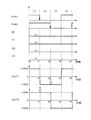
- FIG. 2 shows an example of a time chart in the case of the full step mode
- FIG. 3 shows an example of a time chart in the case of the half step mode. 2 and 3
- the horizontal axis indicates time
- the vertical axis indicates the state of the control signals PHA1 and PHA2 indicating the polarity of the excitation current
- the control signals I01, I11 which determine the voltage division ratio of the target voltage.
- the states of I02 and I12 and the states of excitation currents IOUT1 and IOUT2 are shown.
- control signals I01, I11, I02, and I12 are always set to a low level (Lo), and excitation currents IOUT1 and IOU2 are controlled by control signal PHA1.
- a square wave shape is switched between a + 100% state and a -100% state.
- the excitation current IOUT1 is switched from + 100% to ⁇ 100% as the control signal PHA1 falls from the high level to the low level at time t1, and is controlled at time t3. As the signal PHA1 rises from the low level to the high level, the exciting current IOUT1 is switched from ⁇ 100% to + 100%.
- the excitation current IOUT2 has a phase difference of 90 ° from the excitation current IOUT2, the excitation current IOUT2 is switched from + 100% to ⁇ 100% at time t2, and the excitation current IOUT2 is ⁇ 100 at time t4. From% to + 100%.
- the output signal CLOUT2 of the comparator 132 is in the Lo state.
- the output signal CLOUT2 of the comparator 132 is in the Hi state.
- the timing of detecting the state of the output signal of the comparator may be either when the control signals PHA1 and PHA2 rise or fall. Alternatively, the timing for detecting the state of the output signal of the comparator may be after a predetermined delay time has elapsed from the rise or fall of the control signals PHA1 and PHA2.
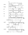
- the states of the control signals I01, I11, I02, and I12 are changed for half the quarter period (ie, 1/8 period) when the combination state of the excitation currents IOUT1 and IOUT2 changes. Be controlled.
- control signals I01 and I11 are set to the Hi state only from time t22 to time t23 and from time t26 to time t27 in FIG.
- control signals I02 and I12 are set to the Hi state only from time t20 to time t21 and from time t24 to time t25 in FIG.
- the excitation currents IOUT1 and IOUT2 are in the 0% state, and the excitation currents IOUT1 and IOUT2 are The waveform can be made closer to a sine wave.
- the current state of the other channel is detected by detecting the current state of the other channel. It can be determined whether or not an abnormality has occurred in the wiring.
- FIG. 4 shows an example in which the control signals I01 and I02 are set to become Lo for 1/8 period and the control signals I11 and I12 are set to Hi for 1/8 period.
- the excitation current level is + 67% between time t31 and time t32, between time t33 and time t34, between time t35 and time t36, and between time t37 and time t38 in FIG.
- An intermediate state of ⁇ 67% can be obtained, and the excitation current can be made closer to a sine wave.
- the timing at which the states of the control signals PHA1, PHA2 are just switched is also the timing at which the level of the excitation current changes to + 100% (or to -100%). For this reason, there is a possibility that a state during charging of the exciting coil is detected and an abnormality cannot be appropriately detected. In such a case, as described above, it is preferable to detect a state after a predetermined delay time from the timing at which the states of the control signals PHA1 and PHA2 are switched.
- control signals I01, I11, I02,... are further output for 1/4 of the 1/4 cycle (that is, 1/16 cycle) in which the polarity combination state of the excitation currents IOUT1, IOUT2 changes.
- the level of the excitation current can be further set to + 33% or ⁇ 33% by the combination of the control signals I01, I11, I02, and I12. Thereby, the waveform of the excitation current can be made closer to a sine wave, and smoother rotation can be realized.
- an abnormality occurs in the wiring of the other channel by detecting the current state of the other channel at an appropriate timing based on the timing at which the control signals PHA1 and PHA2 are switched. It can be determined whether or not.
- FIG. 5 is a functional block diagram for explaining the abnormality detection control executed by the abnormality detection unit 170 in the first embodiment.
- Each functional block described in the functional block diagram of FIG. 5 is realized by hardware or software processing by the abnormality detection unit 170.
- abnormality detection unit 170 includes a current limit detection unit 171, a determination unit 172, and a malfunction prevention unit 173.
- the current limit detection unit 171 receives the oscillation signal OSC from the oscillation circuit 190 and the output signals CLOUT1 and CLOUT2 from the comparators 131 and 132. For each of the output signals CLOUT1 and CLOUT2, the current limit detection unit 171 determines whether or not the output signals CLOUT1 and CLOUT2 become Lo during a predetermined period (T1) determined from the oscillation signal OSC, that is, the output signals CLOUT1 and CLOUT2. It is determined whether CLOUT2 reaches the target voltages VA1 and VA2, respectively, and whether the excitation currents IOUT1 and IOUT2 have reached current limit values corresponding to the target voltages VA1 and VA2.
- T1 predetermined period
- the current limit detection unit 171 sets the corresponding detection signals CLD1 and CLD2 to OFF when the output signals CLOUT1 and CLOUT2 become Lo during the predetermined period. On the other hand, when the output signals CLOUT1 and CLOUT2 remain Hi during the predetermined period, the detection signals CLD1 and CLD2 are set to ON. Then, current limit detection unit 171 outputs detection signals CLD1 and CLD2 to determination unit 172.
- Determination unit 172 receives detection signals CLD1, CLD2 and control signals PHA1, PHA2 from current limit detection unit 171. As described with reference to FIGS. 2 to 4, the determination unit 172 sets the detection signals CLD1 and CLD2 of the other channel to ON at a predetermined timing determined based on the rise or fall of the control signals PHA1 and PHA2. It is determined whether or not.
- the determination unit 172 may have an abnormality in the wiring of the other channel. As a result, the abnormality flags DET1 and DET2 of the corresponding channel are set to ON. When the detection signals CLD1, CLD2 are off, the abnormality flags DET1, DET2 are set off.
- the determination unit 172 outputs the abnormality flags DET1 and DET2 to the malfunction prevention unit 173.
- the malfunction prevention unit 173 is temporarily determined to be abnormal by the determination unit 172 even though there is originally no wiring abnormality due to, for example, a delay in the excitation current rising due to the operating state of the stepping motor 200 or the influence of noise. This is a function to prevent the influence of false detection in the case of failure.
- the malfunction prevention unit 173 receives the abnormality flags DET1, DET2 and the control signals PHA1, PHA2 from the determination unit 172.
- the malfunction prevention unit 173 determines whether or not the abnormality flags DET1 and DET2 are continuously set to ON in the determination unit 172 at a predetermined predetermined number of times (for example, three times) of the control signals PHA1 and PHA2.
- the malfunction prevention unit 173 detects that the abnormality flags DET1 and DET2 are set to ON continuously for a predetermined number of times, the malfunction prevention unit 173 determines that a wiring abnormality has occurred, and in response thereto, an abnormality signal Outputs ALM.
- the abnormality signal ALM is received by an abnormality notification unit (not shown) provided outside or inside the drive circuit 100, and the occurrence of abnormality is notified to the user.
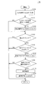
- FIG. 6 is a flowchart for explaining details of the abnormality detection control process executed by the abnormality detection unit 170 in the first embodiment.
- a program stored in advance in the CPU is called from the main routine, and The processing is realized by being executed periodically.
- dedicated hardware electronic circuit
- abnormality detection unit 170 outputs signals CLOUT1 and CLOUT2 (hereinafter referred to as CLOUT1 and CLOUT2) from comparators 131 and 132 at step (hereinafter abbreviated as S) 100. Collectively also referred to as “CLOUT”). Then, in S110, the abnormality detection unit 170 determines whether or not these output signals are in a Hi state for a predetermined period T1.
- abnormality detection unit 170 detects detection signal CLD (hereinafter, CLD1, CLD2) for the corresponding channel in S120. Are also collectively referred to as “CLD”). Thereafter, the process proceeds to S130.
- CLD detection signal
- the abnormality detection unit 170 determines whether or not there is a predetermined detection timing based on a control signal PHA (hereinafter, PHA1 and PHA2 are also collectively referred to as “PHA”).
- PHA1 and PHA2 are also collectively referred to as “PHA”.
- the abnormality detection unit 170 ends the process.
- abnormality detection unit 170 determines whether or not detection signal CLD of the other channel is set to ON. .
- the abnormality detection unit 170 determines that the exciting current is equal to the target value and no wiring abnormality has occurred, and ends the process. To do.
- abnormality detection unit 170 determines that there is a possibility that a wiring abnormality has occurred.
- the abnormality flag DET (hereinafter, DET1 and DET2 are collectively referred to as “DET”) is set to ON.
- the abnormality detection unit 170 determines whether or not the abnormality flag DET has been detected for a predetermined number of cycles (n times: n is a natural number) of the control signal PHA.
- abnormality detection unit 170 terminates the process as an erroneous detection of an abnormal state.
- control signal PHA is detected n times consecutively (YES in S160)
- the process proceeds to S170, and abnormality detection unit 170 determines that a wiring abnormality has occurred. Then, abnormality detection unit 170 outputs abnormality signal ALM in S180.
- Embodiment 2 a stepping motor drive circuit having a function of internally generating the above-described control signal based on information such as a control mode given from the outside will be described.
- FIG. 7 is an overall block diagram of a motor drive system 10A including a stepping motor drive circuit 100A according to the second embodiment.
- FIG. 7 shows a configuration in which a command generation unit 115 is added to the drive circuit 100 described in FIG. 1 of the first embodiment. In FIG. 7, the description of the elements overlapping with those in FIG. 1 will not be repeated.
- drive circuit 100A further includes a command generation unit 115 in addition to the configuration of drive circuit 100 shown in FIG.
- the command generation unit 115 receives a reference clock signal CLK, a control mode signal MOD, a signal CW_CCW indicating a rotation direction, and an enable signal ENB from the outside of the circuit.
- the control mode signal MOD is a signal that determines which of the full step mode, the half step mode, and the quarter step mode described with reference to FIGS. 2 to 4 of the first embodiment is selected.
- the command generation unit 115 generates control signals PHA1 and PHA2 based on these pieces of information, and outputs them to the logic control unit 140 and the abnormality detection unit 170. Further, the command generator 115 generates control signals I01, I11, I02, and I12 and outputs them to the D / A converter 120.
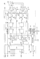
- FIG. 8 is an overall block diagram of a motor drive system 10B including a stepping motor drive circuit 100B according to the third embodiment.
- the abnormality detection unit 170 in FIG. 1 of the first embodiment is replaced with the abnormality detection unit 170B, and a resistor R10 and a capacitor C10 connected in parallel provided outside the drive circuit are connected to the oscillation circuit 190. It has become a thing.
- drive circuit 100B receives a power save signal PS that is a start signal from the outside.
- the drive circuit 100B is powered on by supplying power to each circuit in the drive circuit 100B.
- the power save signal PS is turned off (low level)
- the standby state is entered, and the output of the excitation current to the stepping motor 200 is stopped.
- the logic circuit 141 of the channel CH1 receives the phase signal PHA1 indicating the polarity of the excitation current IOUT1, the output signal CLOUT1 of the comparator 131, and the enable signal ENB. Then, the logic circuit 141 generates a drive signal using these signals and a control signal PWM set by the PWM control unit based on the oscillation signal OSC from the oscillation circuit 190.
- the enable signal ENB is a signal for enabling the logic control unit 140 (logic circuits 141 and 142).
- the enable signal ENB When the enable signal ENB is turned on (high level), the logic control unit 140 is enabled and H When the transistors included in the bridges 161 and 162 are driven, an excitation current is supplied from the drive circuit 100B to the stepping motor 200.
- the enable signal ENB is turned off (low level)
- the logic control unit 140 is disabled, and the supply of the excitation current from the drive circuit 100B to the stepping motor 200 is stopped.
- the oscillation circuit 190 is connected to a resistor R10 and a capacitor C10 connected in parallel.
- the period of the chopping operation as will be described later with reference to FIG. 10 is determined by the parallel circuit of the resistor R10 and the capacitor C10.
- the abnormality detector 170B includes phase signals PHA1 and PHA2 indicating the polarities of the excitation currents IOUT1 and IOUT2, output signals CLOUT1 and CLOUT2 of the comparators 131 and 132, an oscillation signal OSC from the oscillation circuit 190, and an enable signal ENB.
- the power save signal PS is received. Based on this information, the abnormality detection unit 170B executes abnormality detection control for detecting whether or not an abnormality has occurred in the wiring that supplies the excitation currents IOUT1 and IOUT2 from the drive circuit 100B to the stepping motor 200.
- FIG. 9 shows a time chart showing a general output current in the case of the full step mode as an example.
- the horizontal axis represents time, and the vertical axis represents the states of the phase signals PHA1 and PHA2 indicating the polarity of the excitation current, the states of the control signals I01, I11, I02, and I12 that determine the voltage division ratio of the target voltage, and the excitation current IOUT1. , IOUT2 is shown.
- the case of the full step mode will be described as an example.
- each control signal is only output for a half of a quarter period (that is, a 1/8 period) during which the combination state of the polarities of the excitation currents IOUT1 and IOUT2 changes.
- a half step mode in which the states of I01, I11, I02, and I12 are controlled, or for a quarter (ie, 1/16 period) of a quarter period in which the combination state of the polarity of the excitation currents IOUT1 and IOUT2 changes.
- the quarter step mode for controlling the states of the control signals I01, I11, I02, and I12 the following control can be applied.
- control signals I01, I11, I02, and I12 are always set to a low level (Lo), and excitation currents IOUT1 and IOU2 are applied to phase signals PHA1 and PHA2, respectively. Synchronously, it switches to a square waveform between + 100% and ⁇ 100%.
- the excitation current IOUT1 switches from + 100% to ⁇ 100% as the phase signal PHA1 falls from the high level to the low level at time t41, and the phase at time t43. As the signal PHA1 rises from the low level to the high level, the exciting current IOUT1 is switched from ⁇ 100% to + 100%.
- the excitation current IOUT2 has a phase difference of 90 ° from the excitation current IOUT2, the excitation current IOUT2 is switched from + 100% to ⁇ 100% at time t42, and the excitation current IOUT2 is ⁇ 100 at time t44. From% to + 100%.
- an excitation current closer to a sine wave can be supplied than in the full step mode of FIG. 9 by using an intermediate level excitation current.
- FIG. 10 is a diagram for explaining in more detail the state of the excitation current IOUT1 from time 0 to time t41 in FIG. 9, for example.
- the horizontal axis represents time
- the vertical axis represents excitation current IOUT, voltage RNF indicating excitation current IOUT, oscillation signal OSC, and output signal CLOUT.
- the signals for channels CH1 and CH2 are generically named, for example, IOUT1 and IOUT2 are referred to as “IOUT” or the like.
- the output current IOUT is controlled to be the target current IREF by using a feedback loop as shown in FIG.
- the oscillation signal OSC changes in a triangular waveform between the potential VCRH and the potential VCRL by the parallel circuit of the resistor R10 and the capacitor C10 shown in FIG. More specifically, when the oscillation signal OSC becomes the potential VCRL, the capacitor C10 of the parallel circuit is charged, and the oscillation signal OSC increases to the potential VCRH. When the oscillation signal OSC becomes the potential VCRH, the charging of the capacitor C10 is stopped, and the charge stored in the capacitor C10 is discharged by the resistor R10. When the potential of the oscillation signal OSC decreases to the potential VCRL due to this discharge, the capacitor C10 is charged again.
- the chopping cycle TCH of the current control circuit 130 is determined by the resistor R10 and the capacitor C10 of the parallel circuit.
- the output signal CLOUT is turned on, and the logic control unit 140 and the pre-driver unit 150 start driving the H-bridge transistor.
- the excitation current IOUT increases.
- the voltage RNF increases.
- the output signal CLOUT remains on and the supply of the excitation current IOUT is continued.
- the output signal CLOUT from the comparator is turned off (time t51, t53, t55, t57).
- the driving of the H bridge is stopped by the logic control unit 140. Then, since no current flows through the resistors R1 and R2, the voltage RNF is lowered to the ground potential.
- the oscillation signal OSC rises again after the oscillation signal OSC has dropped to the potential VCRL, the output signal CLOUT is turned on, the H bridge is driven, and the output current IOUT increases.
- the phase signal PHA indicating the polarity of the excitation current IOUT and the control signals I01, I02, I11, and I12 indicate the target current IREF.
- the output current IOUT is always controlled to be a predetermined target current IREF by repeating the chopping operation as described above in a short chopping cycle TCH.
- the voltage RNF reaches the target voltage VA in each chopping cycle TCH, that is, the excitation current IOUT is the current.
- the target current IREF which is a limit
- the output signal CLOUT is turned off from on.
- the excitation signal IOUT does not reach the current limit, and the output signal CLOUT remains on.
- the path through which the excitation current is supplied by detecting whether the excitation current IOUT has reached the current limit, that is, whether the output signal CLOUT has changed from on to off. Detect abnormalities.
- FIG. 11 is a functional block diagram for explaining the abnormality detection control executed by the abnormality detection unit 170B in the third embodiment.
- Each functional block described in the functional block diagram of FIG. 11 is realized by hardware or software processing by the abnormality detection unit 170B.
- abnormality detection unit 170B includes a current limit detection unit 171B, a determination unit 172B, and a malfunction prevention unit 173B.
- the current limit detection unit 171B receives the oscillation signal OSC from the oscillation circuit 190 and the output signal CLOUT from the comparator. For the output signal CLOUT, the current limit detection unit 171B determines whether or not the output signal CLOUT has been turned from on to off during each chopping period described in FIG. 10, that is, the output signal CLOUT has reached the target voltage VA. Then, it is determined whether or not the excitation current IOUT has reached a current limit value corresponding to the target voltage VA.
- the current limit detection unit 171B sets the detection signal CLD to off when the output signal CLOUT is turned off from on during the predetermined period. On the other hand, when the output signal CLOUT remains on during the predetermined period, the detection signal CLD is set to on. Then, the current limit detection unit 171B outputs the detection signal CLD to the determination unit 172B.
- Determination unit 172B receives detection signal CLD, phase signal PHA, enable signal ENB, and power save signal PS from current limit detection unit 171B. For example, the determination unit 172B counts the number of times that the detection signal CLD has been turned off in a predetermined period in which the target current IREF is constant, which is determined based on the rising or falling edge of the phase signal PHA.
- the determination unit 172B may have an abnormality in the wiring of the channel. As a result, the abnormality flag DET of the corresponding channel is set to ON. When the number of times the detection signal CLD is turned off exceeds a predetermined number, it is determined that the wiring is normal, and the abnormality flag DET is set to off. Then, the determination unit 172B outputs the abnormality flag DET to the malfunction prevention unit 173B.
- the PHA signal is not switched unless the stepping motor 200 is actually driven (rotated). Then, if the determination is made based only on the timing based on the switching of the phase signal PHA, the wiring abnormality cannot be determined when the stepping motor 200 is in the stopped state. Therefore, in addition to the timing of switching the phase signal PHA, the timing when the power save signal PS is turned on and the enable signal ENB is turned on, that is, the timing when the excitation current is supplied from the drive circuit 100B to the stepping motor 200. Also in the period determined based on the above, it is preferable to determine the abnormality of the wiring as described above. Further, when the PHA signal is not switched for a certain period, the abnormality may be determined at predetermined time intervals.
- the malfunction prevention unit 173B is temporarily determined to be abnormal by the determination unit 172B even though there is originally no wiring abnormality due to, for example, the delay in the rise of the excitation current due to the operating state of the stepping motor 200 or the influence of noise. This is a function to prevent the influence of false detection in the case of failure.
- the malfunction prevention unit 173B receives the abnormality flag DET and the phase signal PHA from the determination unit 172B.
- the malfunction prevention unit 173B determines whether or not the abnormality flag DET is continuously set to ON in the determination unit 172B at a predetermined cycle (for example, three times) of the phase signal PHA. Then, when the malfunction prevention unit 173B detects that the abnormality flag DET is set to ON continuously for a predetermined number of times, the malfunction prevention unit 173B determines that a wiring abnormality has occurred, and responds to the abnormality signal ALM. Output.
- the abnormality signal ALM is received by an abnormality notification unit (not shown) provided outside or inside the drive circuit 100B, and the occurrence of abnormality is notified to the user.
- the abnormality flag DET determined at predetermined time intervals continues to be abnormal for a predetermined number of times. May indicate that a wiring abnormality has occurred.
- FIG. 12 is a flowchart for explaining details of the abnormality detection control process executed by the abnormality detection unit 170B in the third embodiment.
- a program stored in advance in the CPU is called from the main routine and The processing is realized by being executed periodically.
- dedicated hardware electronic circuit
- abnormality detection unit 170B obtains output signal CLOUT from the comparator at step (hereinafter, step is abbreviated as S) 100B.
- step is abbreviated as S) 100B.
- abnormality detection unit 170B determines whether or not output signal CLOUT has fallen from on to off, that is, whether or not excitation current IOUT has reached the current limit.
- abnormality detection unit 170B sets detection signal CLD for that channel to ON in S220. Thereafter, the process proceeds to S230.
- the abnormality detection unit 170B determines whether or not a predetermined detection period determined based on the phase signal PHA or the power save signal PS and the enable signal ENB.
- abnormality detection unit 170B ends the process and returns the process to the main routine.
- abnormality detection unit 170B determines whether or not the number CNT of times that detection signal CLD has been turned on is greater than a predetermined threshold value ⁇ at the end of the detection period.
- abnormality detection unit 170B assumes that a wiring abnormality may have occurred, Is set to ON.
- the abnormality detection unit 170B determines whether or not the abnormality flag DET has been continuously detected a predetermined number of times (n times: n is a natural number).
- abnormality detection unit 170B ends the process on the assumption that there is a high possibility of an erroneous detection of an abnormal state.
- abnormality flag DET If abnormality flag DET is detected n times consecutively (YES in S270), the process proceeds to S280, and abnormality detection unit 170B determines that a wiring abnormality has occurred. Then, abnormality detection unit 170B outputs abnormality signal ALM in S290.
- a stepping motor drive circuit having a function of internally generating the above-described control signal based on information such as a control mode given from the outside will be described.
- FIG. 13 is an overall block diagram of a motor drive system 10C including a stepping motor drive circuit 100C according to the fourth embodiment.
- FIG. 13 shows a configuration in which a command generation unit 115C is added to the drive circuit 100B described in FIG. 8 of the third embodiment. In FIG. 13, the description of the elements overlapping with those in FIG. 8 will not be repeated.
- drive circuit 100C further includes a command generation unit 115C in addition to the configuration of drive circuit 100B shown in FIG.
- the command generation unit 115C receives a reference clock signal CLK, a control mode signal MOD, a signal CW_CCW indicating a rotation direction, and an enable signal ENB from the outside of the circuit.
- the control mode signal MOD is a signal that determines which one of the full step mode, the half step mode, and the quarter step mode is selected.
- the command generation unit 115C generates phase signals PHA1 and PHA2 based on these pieces of information and outputs them to the logic control unit 140 and the abnormality detection unit 170B. Further, command generation unit 115C generates control signals I01, I11, I02, and I12 and outputs them to D / A converter 120.
- the same abnormality detection control as that of the third embodiment can be applied to the circuit having such a configuration.
- a configuration for detecting an abnormality in a wiring to which an excitation current is supplied will be described based on a comparison between a voltage RNF indicating the excitation current IOUT and a reference voltage different from the target voltage VA.
- FIG. 14 is an overall block diagram of a motor drive system 10D including a stepping motor drive circuit 100D according to the fifth embodiment.
- FIG. 14 shows a configuration in which comparators 131 # and 132 # are added to the drive circuit 100B described in FIG. 8 of the third embodiment. In FIG. 14, the description of the same elements as those in FIG. 8 will not be repeated.
- drive circuit 100D further includes comparators 131 # and 132 # in addition to the configuration of drive circuit 100B shown in FIG.
- the comparator 131 # compares the reference voltage source B1 with the voltage RNF1 indicating the excitation current IOUT1, and generates an output signal CLOUT1 # indicating the comparison result. Comparator 131 # sets output signal CLOUT1 # off when voltage RNF1 reaches the reference voltage, and sets output signal CLOUT1 # on when voltage RNF1 does not reach the reference voltage. To do. Comparator 131 # outputs output signal CLOUT1 # to abnormality detection unit 170B.
- the comparator 132 # compares the reference voltage source B2 with the voltage RNF2 indicating the excitation current IOUT2, and generates an output signal CLOUT2 # indicating the comparison result. Comparator 132 # sets output signal CLOUT2 # off when voltage RNF2 reaches the reference voltage, and sets output signal CLOUT2 # on when voltage RNF2 does not reach the reference voltage. To do. Comparator 132 # outputs output signal CLOUT2 # to abnormality detection unit 170B.
- the voltages of the reference voltage sources B1 and B2 are set smaller than the target voltage VA.
- the voltages of the reference voltages B1 and B2 are set based on, for example, the minimum set current value of the stepping motor 200 determined depending on the application to be used. More preferably, the reference voltage is smaller than the minimum set current value. Set to a value. As an example, when the operating current range of the stepping motor 200 is 100 mA to 1 A (that is, the minimum set current value is 100 mA), the reference voltage can be set to a value corresponding to a current value of 30 to 50 mA.
- the abnormality detection unit 170B receives the output signals CLOUT1 # and CLOUT2 # from the comparators 131 # and 132 #. As in the case of the third embodiment, the abnormality detection unit 170B detects the number of times the output signals CLOUT1 # and CLOUT2 # are turned off within a predetermined period, thereby detecting an abnormality in the wiring to which the excitation current is supplied. To detect.
- FIG. 15 is a time chart corresponding to FIG. 10 of the third embodiment.
- the output signal CLOUT in FIG. 10 is replaced with an output signal CLOUT # (hereinafter, the output signals CLOUT1 # and CLOUT2 # are collectively referred to as “CLOUT #”).
- the output signal CLOUT # is switched from on to off when the voltage RNF reaches the reference voltage VB lower than the target voltage VA (time t61, t64, t67, t70).
- FIG. 16 is a flowchart for explaining details of the abnormality detection control process executed by the abnormality detection unit 170B in the fifth embodiment.
- steps S200 and S210 in FIG. 12 of the third embodiment are replaced with S200 # and S210 #.
- the comparison is performed.
- the detection signal CLD is set based on the output signals CLOUT1 # and CLOUT2 # from the devices 131 # and 132 # (S220). Since the processing after S220 is the same as the description of FIG. 12, it will not be repeated.
- a command generation unit may be provided in the drive circuit.
- the driving circuits described in Embodiments 1 to 5 may be configured to construct a part or all of the circuits and functions included in the driving circuits using individual electronic devices, or the entire circuits may be configured. It is good also as a structure constructed
- 10, 10A-10D motor drive system 100, 100A-100D drive circuit, 110 input buffer, 115, 115C command generator, 120 D / A converter, 130 current control circuit, 131, 131 #, 132, 132 # comparator , 140 logic control unit, 141, 142 logic circuit, 150 pre-driver unit, 151, 152 pre-driver, 161, 162 H bridge, 170, 170B abnormality detection unit, 171, 171B current limit detection unit, 172, 172B determination unit, 173, 173B malfunction prevention unit, 180 PWM control unit, 190 oscillation circuit, 200 stepping motor, 210 rotor, B1, B2 reference voltage, C10 capacitor, CH1, CH2 channel, L1, L2 excitation coil, N11, 12, N21, N22 nodes, Q11 ⁇ Q14, Q21 ⁇ Q24 transistors, R1, R2, R10 resistors, T11 ⁇ T13, T21 ⁇ T23 terminal.
Landscapes
- Engineering & Computer Science (AREA)
- Power Engineering (AREA)
- Control Of Stepping Motors (AREA)
Abstract
La présente invention concerne un circuit d'entraînement (100) pour un moteur pas à pas (200) qui comprend un convertisseur N/A (120), une unité de commande du courant (130) comprenant des unités de comparaison (131, 132) et une unité de détection d'erreurs (170). Le convertisseur N/A (CNA) (120) génère des tensions cibles (VA1, VA2) indiquant des valeurs cibles pour des courants d'excitation stipulés sur la base d'une tension de référence (VREF) indiquant la limite supérieure pour des courants d'excitation (IOUT1, IOUT2) circulant vers le moteur pas à pas (200). L'unité de commande du courant (130) commande les courants d'excitation sur la base des tensions cibles. Les unités de comparaison (131, 132) comparent les tensions (RNF1, RNF2) qui correspondent aux courants d'excitation avec les tensions cibles. L'unité de détection d'erreurs (170) détecte des erreurs dans le câblage entre le circuit d'entraînement (100) et le moteur pas à pas (200) sur la base de signaux de sortie (CLOUT1, CLOUT2) à partir des unités de comparaison et de signaux de commande (PHA1, PHA2) indiquant la polarité des courants d'excitation.
Priority Applications (2)
| Application Number | Priority Date | Filing Date | Title |
|---|---|---|---|
| US13/981,391 US9654040B2 (en) | 2011-01-25 | 2012-01-23 | Drive circuit of stepping motor, integrated circuit thereof, and electronic equipment including same, and method for controlling drive circuit of stepping motor |
| CN201280011448.2A CN103404020B (zh) | 2011-01-25 | 2012-01-23 | 步进电机的驱动电路、其集成电路和包括该集成电路的电子设备以及步进电机的驱动电路的控制方法 |
Applications Claiming Priority (4)
| Application Number | Priority Date | Filing Date | Title |
|---|---|---|---|
| JP2011-012839 | 2011-01-25 | ||
| JP2011012839A JP5785718B2 (ja) | 2011-01-25 | 2011-01-25 | ステッピングモータの駆動回路、その集積回路およびそれを備える電子機器 |
| JP2011085361A JP5835923B2 (ja) | 2011-04-07 | 2011-04-07 | ステッピングモータの駆動回路および集積回路 |
| JP2011-085361 | 2011-04-07 |
Publications (1)
| Publication Number | Publication Date |
|---|---|
| WO2012102232A1 true WO2012102232A1 (fr) | 2012-08-02 |
Family
ID=46580799
Family Applications (1)
| Application Number | Title | Priority Date | Filing Date |
|---|---|---|---|
| PCT/JP2012/051325 Ceased WO2012102232A1 (fr) | 2011-01-25 | 2012-01-23 | Circuit d'entraînement pour un moteur pas à pas, son circuit intégré et dispositif électronique le comprenant, et procédé de commande pour un circuit d'entraînement de moteur pas à pas |
Country Status (3)
| Country | Link |
|---|---|
| US (1) | US9654040B2 (fr) |
| CN (1) | CN103404020B (fr) |
| WO (1) | WO2012102232A1 (fr) |
Families Citing this family (16)
| Publication number | Priority date | Publication date | Assignee | Title |
|---|---|---|---|---|
| JP6384201B2 (ja) | 2014-08-28 | 2018-09-05 | セイコーエプソン株式会社 | 集積回路装置及び電子機器 |
| WO2016147511A1 (fr) * | 2015-03-19 | 2016-09-22 | 三菱電機株式会社 | Dispositif de commande de moteur pas-à-pas, et épurateur d'air incorporant un moteur pas-à-pas |
| JP6641794B2 (ja) | 2015-08-28 | 2020-02-05 | 株式会社リコー | モータ駆動装置、モータ制御装置、搬送装置及びモータ駆動方法 |
| CN105553357B (zh) * | 2015-12-10 | 2019-01-01 | 中国航空工业集团公司西安航空计算技术研究所 | 一种固定占空比步进电机恒流驱动系统及方法 |
| EP3291438B1 (fr) * | 2016-08-30 | 2021-11-10 | Valeo Klimasysteme GmbH | Procédé de détection de blocage d'un moteur pas à pas électrique, moteur pas à pas électrique et dispositif de chauffage, de ventilation et/ou un système de climatisation comprenant un moteur pas à pas électrique |
| RU173260U1 (ru) * | 2016-12-19 | 2017-08-21 | Федеральное государственное автономное образовательное учреждение высшего образования "Крымский федеральный университет имени В.И. Вернадского" | Устройство для обнаружения отказов в шаговом электроприводе |
| JP6826075B2 (ja) * | 2018-07-03 | 2021-02-03 | ミネベアミツミ株式会社 | モータ駆動制御装置及びモータ駆動制御装置の制御方法 |
| CN108964539A (zh) * | 2018-07-24 | 2018-12-07 | 中国石油集团渤海钻探工程有限公司 | 一种用于底部钻具动力执行机构的电机驱动电路及方法 |
| JP7387268B2 (ja) * | 2019-02-15 | 2023-11-28 | ローム株式会社 | ステッピングモータの駆動回路、それを用いた電子機器 |
| JP7224204B2 (ja) * | 2019-02-26 | 2023-02-17 | ローム株式会社 | ステッピングモータの駆動回路、それを用いた電子機器 |
| DE112020004991T5 (de) * | 2019-10-15 | 2022-07-14 | Ngk Spark Plug Co., Ltd. | Sensorsystem und Sensorsystemfehlererfassungsverfahren |
| JP7549000B2 (ja) * | 2020-03-27 | 2024-09-10 | ローム株式会社 | ドライバ装置 |
| JP7390621B2 (ja) * | 2020-06-25 | 2023-12-04 | パナソニックIpマネジメント株式会社 | ステッピングモータ異常検知装置 |
| ES3034239T3 (en) * | 2020-08-28 | 2025-08-14 | Panasonic Ip Man Co Ltd | Stepping motor abnormality detecting device |
| DE102022134623A1 (de) * | 2022-12-22 | 2024-06-27 | Middex - Electronic GmbH | System zur Zustandsüberwachung eines elektrischen Motors |
| CN116604954B (zh) * | 2023-04-25 | 2024-02-23 | 珠海芯烨电子科技有限公司 | 一种用于热敏打印机步进电机的控制方法 |
Citations (3)
| Publication number | Priority date | Publication date | Assignee | Title |
|---|---|---|---|---|
| JPH02184296A (ja) * | 1989-01-09 | 1990-07-18 | Asmo Co Ltd | ステップモータの異常検出装置 |
| JPH04261396A (ja) * | 1991-02-14 | 1992-09-17 | Nippondenso Co Ltd | ステッピングモータの異常監視装置 |
| JP2008029145A (ja) * | 2006-07-24 | 2008-02-07 | Rohm Co Ltd | ステッピングモータの駆動回路および電子機器 |
Family Cites Families (7)
| Publication number | Priority date | Publication date | Assignee | Title |
|---|---|---|---|---|
| US4748954A (en) * | 1984-07-16 | 1988-06-07 | Nippon Soken, Inc. | Electrostrictive actuator device and fuel injection device using same |
| JP2545641B2 (ja) * | 1990-08-09 | 1996-10-23 | 本田技研工業株式会社 | パルスモータの駆動制御装置 |
| JPH1127991A (ja) * | 1997-07-07 | 1999-01-29 | Canon Inc | 画像形成装置 |
| JP3374361B2 (ja) * | 1997-04-04 | 2003-02-04 | 矢崎総業株式会社 | 車両の異常電流検出方法及び車両の異常電流検出装置並びに車両用電源供給装置 |
| JP3938920B2 (ja) * | 2004-04-02 | 2007-06-27 | 日本サーボ株式会社 | ステッピングモータの制御装置 |
| JP4177387B2 (ja) * | 2006-05-01 | 2008-11-05 | 三菱電機株式会社 | モータ制御装置 |
| JP2011069336A (ja) * | 2009-09-28 | 2011-04-07 | Keihin Corp | 内燃機関の制御装置 |
-
2012
- 2012-01-23 WO PCT/JP2012/051325 patent/WO2012102232A1/fr not_active Ceased
- 2012-01-23 CN CN201280011448.2A patent/CN103404020B/zh not_active Expired - Fee Related
- 2012-01-23 US US13/981,391 patent/US9654040B2/en not_active Expired - Fee Related
Patent Citations (3)
| Publication number | Priority date | Publication date | Assignee | Title |
|---|---|---|---|---|
| JPH02184296A (ja) * | 1989-01-09 | 1990-07-18 | Asmo Co Ltd | ステップモータの異常検出装置 |
| JPH04261396A (ja) * | 1991-02-14 | 1992-09-17 | Nippondenso Co Ltd | ステッピングモータの異常監視装置 |
| JP2008029145A (ja) * | 2006-07-24 | 2008-02-07 | Rohm Co Ltd | ステッピングモータの駆動回路および電子機器 |
Also Published As
| Publication number | Publication date |
|---|---|
| US9654040B2 (en) | 2017-05-16 |
| CN103404020B (zh) | 2016-12-07 |
| US20130307460A1 (en) | 2013-11-21 |
| CN103404020A (zh) | 2013-11-20 |
Similar Documents
| Publication | Publication Date | Title |
|---|---|---|
| WO2012102232A1 (fr) | Circuit d'entraînement pour un moteur pas à pas, son circuit intégré et dispositif électronique le comprenant, et procédé de commande pour un circuit d'entraînement de moteur pas à pas | |
| CN101361260B (zh) | 电机驱动电路、驱动方法、电机装置及使用了它的电子设备 | |
| US7710173B2 (en) | Duty cycle correction circuit and delay locked loop circuit including the same | |
| US8004338B2 (en) | Pulse generator | |
| US8519747B2 (en) | Driver and high voltage drive circuit including the same | |
| CA2770381C (fr) | Circuit generateur de temps mort et appareil de commande de moteur | |
| JP2013162568A (ja) | モータ駆動制御システム | |
| US9793839B2 (en) | Motor control circuit | |
| US20180019747A1 (en) | Signal transmission circuit and driving device for switching element | |
| JP5785718B2 (ja) | ステッピングモータの駆動回路、その集積回路およびそれを備える電子機器 | |
| JP3833199B2 (ja) | 相補信号発生回路 | |
| US7466093B2 (en) | Motor drive unit and electric apparatus having a motor | |
| US20220077851A1 (en) | Electronic circuitry and power converter | |
| JP5835923B2 (ja) | ステッピングモータの駆動回路および集積回路 | |
| KR20160109578A (ko) | 듀티 보정 회로 및 그를 포함하는 이미지 센싱 장치 | |
| JP2008029146A (ja) | モータの駆動回路および電子機器 | |
| JP6456212B2 (ja) | 制御装置及び駆動装置 | |
| US10644679B2 (en) | Level shift circuit | |
| JP2008029145A (ja) | ステッピングモータの駆動回路および電子機器 | |
| JP7691287B2 (ja) | ブリッジ回路の駆動回路、それを用いたモータ駆動装置、電子機器 | |
| JP6456211B2 (ja) | 制御装置及び駆動装置 | |
| JP2012065471A (ja) | モータ駆動回路 | |
| JP6456210B2 (ja) | 制御装置及び駆動装置 | |
| JP4783189B2 (ja) | 駆動回路 | |
| JP2025008085A (ja) | ブリッジ回路の駆動装置 |
Legal Events
| Date | Code | Title | Description |
|---|---|---|---|
| 121 | Ep: the epo has been informed by wipo that ep was designated in this application |
Ref document number: 12739973 Country of ref document: EP Kind code of ref document: A1 |
|
| WWE | Wipo information: entry into national phase |
Ref document number: 13981391 Country of ref document: US |
|
| NENP | Non-entry into the national phase |
Ref country code: DE |
|
| 122 | Ep: pct application non-entry in european phase |
Ref document number: 12739973 Country of ref document: EP Kind code of ref document: A1 |