WO2012105232A1 - Procédé de lecture de données d'élément d'enregistrement non volatil et dispositif d'enregistrement non volatil - Google Patents
Procédé de lecture de données d'élément d'enregistrement non volatil et dispositif d'enregistrement non volatil Download PDFInfo
- Publication number
- WO2012105232A1 WO2012105232A1 PCT/JP2012/000608 JP2012000608W WO2012105232A1 WO 2012105232 A1 WO2012105232 A1 WO 2012105232A1 JP 2012000608 W JP2012000608 W JP 2012000608W WO 2012105232 A1 WO2012105232 A1 WO 2012105232A1
- Authority
- WO
- WIPO (PCT)
- Prior art keywords
- resistance
- nonvolatile memory
- memory element
- resistance state
- value
- Prior art date
- Legal status (The legal status is an assumption and is not a legal conclusion. Google has not performed a legal analysis and makes no representation as to the accuracy of the status listed.)
- Ceased
Links
Images


Classifications
-
- G—PHYSICS
- G11—INFORMATION STORAGE
- G11C—STATIC STORES
- G11C13/00—Digital stores characterised by the use of storage elements not covered by groups G11C11/00, G11C23/00, or G11C25/00
- G11C13/0002—Digital stores characterised by the use of storage elements not covered by groups G11C11/00, G11C23/00, or G11C25/00 using resistive RAM [RRAM] elements
- G11C13/0021—Auxiliary circuits
- G11C13/004—Reading or sensing circuits or methods
-
- G—PHYSICS
- G11—INFORMATION STORAGE
- G11C—STATIC STORES
- G11C13/00—Digital stores characterised by the use of storage elements not covered by groups G11C11/00, G11C23/00, or G11C25/00
- G11C13/0002—Digital stores characterised by the use of storage elements not covered by groups G11C11/00, G11C23/00, or G11C25/00 using resistive RAM [RRAM] elements
- G11C13/0007—Digital stores characterised by the use of storage elements not covered by groups G11C11/00, G11C23/00, or G11C25/00 using resistive RAM [RRAM] elements comprising metal oxide memory material, e.g. perovskites
-
- G—PHYSICS
- G11—INFORMATION STORAGE
- G11C—STATIC STORES
- G11C13/00—Digital stores characterised by the use of storage elements not covered by groups G11C11/00, G11C23/00, or G11C25/00
- G11C13/0002—Digital stores characterised by the use of storage elements not covered by groups G11C11/00, G11C23/00, or G11C25/00 using resistive RAM [RRAM] elements
- G11C13/0021—Auxiliary circuits
- G11C13/004—Reading or sensing circuits or methods
- G11C2013/0054—Read is performed on a reference element, e.g. cell, and the reference sensed value is used to compare the sensed value of the selected cell
-
- H—ELECTRICITY
- H10—SEMICONDUCTOR DEVICES; ELECTRIC SOLID-STATE DEVICES NOT OTHERWISE PROVIDED FOR
- H10B—ELECTRONIC MEMORY DEVICES
- H10B63/00—Resistance change memory devices, e.g. resistive RAM [ReRAM] devices
- H10B63/20—Resistance change memory devices, e.g. resistive RAM [ReRAM] devices comprising selection components having two electrodes, e.g. diodes
- H10B63/22—Resistance change memory devices, e.g. resistive RAM [ReRAM] devices comprising selection components having two electrodes, e.g. diodes of the metal-insulator-metal type
-
- H—ELECTRICITY
- H10—SEMICONDUCTOR DEVICES; ELECTRIC SOLID-STATE DEVICES NOT OTHERWISE PROVIDED FOR
- H10B—ELECTRONIC MEMORY DEVICES
- H10B63/00—Resistance change memory devices, e.g. resistive RAM [ReRAM] devices
- H10B63/30—Resistance change memory devices, e.g. resistive RAM [ReRAM] devices comprising selection components having three or more electrodes, e.g. transistors
-
- H—ELECTRICITY
- H10—SEMICONDUCTOR DEVICES; ELECTRIC SOLID-STATE DEVICES NOT OTHERWISE PROVIDED FOR
- H10N—ELECTRIC SOLID-STATE DEVICES NOT OTHERWISE PROVIDED FOR
- H10N70/00—Solid-state devices having no potential barriers, and specially adapted for rectifying, amplifying, oscillating or switching
- H10N70/011—Manufacture or treatment of multistable switching devices
- H10N70/021—Formation of switching materials, e.g. deposition of layers
- H10N70/026—Formation of switching materials, e.g. deposition of layers by physical vapor deposition, e.g. sputtering
-
- H—ELECTRICITY
- H10—SEMICONDUCTOR DEVICES; ELECTRIC SOLID-STATE DEVICES NOT OTHERWISE PROVIDED FOR
- H10N—ELECTRIC SOLID-STATE DEVICES NOT OTHERWISE PROVIDED FOR
- H10N70/00—Solid-state devices having no potential barriers, and specially adapted for rectifying, amplifying, oscillating or switching
- H10N70/20—Multistable switching devices, e.g. memristors
- H10N70/24—Multistable switching devices, e.g. memristors based on migration or redistribution of ionic species, e.g. anions, vacancies
-
- H—ELECTRICITY
- H10—SEMICONDUCTOR DEVICES; ELECTRIC SOLID-STATE DEVICES NOT OTHERWISE PROVIDED FOR
- H10N—ELECTRIC SOLID-STATE DEVICES NOT OTHERWISE PROVIDED FOR
- H10N70/00—Solid-state devices having no potential barriers, and specially adapted for rectifying, amplifying, oscillating or switching
- H10N70/801—Constructional details of multistable switching devices
- H10N70/821—Device geometry
- H10N70/826—Device geometry adapted for essentially vertical current flow, e.g. sandwich or pillar type devices
-
- H—ELECTRICITY
- H10—SEMICONDUCTOR DEVICES; ELECTRIC SOLID-STATE DEVICES NOT OTHERWISE PROVIDED FOR
- H10N—ELECTRIC SOLID-STATE DEVICES NOT OTHERWISE PROVIDED FOR
- H10N70/00—Solid-state devices having no potential barriers, and specially adapted for rectifying, amplifying, oscillating or switching
- H10N70/801—Constructional details of multistable switching devices
- H10N70/881—Switching materials
- H10N70/883—Oxides or nitrides
- H10N70/8833—Binary metal oxides, e.g. TaOx
Definitions
- Patent Document 1 One is a perovskite material (Pr (1-x) Ca x MnO 3 (PCMO), LaSrMnO 3 (LSMO), GdBaCo x O y (GBCO), etc.) disclosed in Patent Document 1 or the like as a resistance change layer.
- This is a variable resistance nonvolatile memory element used.
- the unipolar switching operation is an operation mode in which the resistance value is changed by applying electric pulses of the same polarity and different magnitudes to the lower electrode and the upper electrode, which are disclosed in Patent Document 2 and the like.
- the length (pulse width) of the electrical pulse it is necessary to change not only the magnitude of the voltage but also the length (pulse width) of the electrical pulse at the same time. For example, it is necessary to use two types of electrical pulses having a length of nanosecond order and a length of microsecond order.
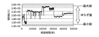
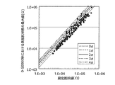
- a non-volatile memory element is an element that has the property that after information is electrically stored, the information is not volatilized (disappeared, degraded, or changed) even when the power is turned off. . Therefore, one of the most important characteristics required for nonvolatile memory elements is high information storage. In other words, the nonvolatile memory element needs to have the ability to retain information without deterioration once written. The higher the information retention capability, the better. However, in general, in any nonvolatile memory element, it is unavoidable that stored information changes within a finite time.
- an information read error may occur.
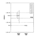
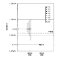
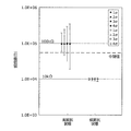
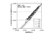
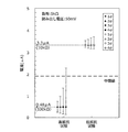
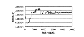
- the case where the set resistance value of the nonvolatile memory element is 120 k ⁇ and half of that value is 60 k ⁇ is considered. That is, a resistance state of 60 k ⁇ or more is defined as a high resistance state, and a resistance state of 60 k ⁇ or less is defined as a low resistance state. Then, when the resistance of the nonvolatile memory element is read at about 1000 seconds after setting the resistance, the resistance value is 50 k ⁇ , and it is determined that the nonvolatile memory element is in the low resistance state.
- the standard electrode potential of the second transition metal is preferably lower than the standard electrode potential of the first transition metal.
- the following method is preferable as the data reading method of the resistance change type nonvolatile memory element. That is, when a voltage having a first polarity (for example, negative polarity) is applied between the first and second electrodes, the resistance between the first and second electrodes is reduced to the first resistance state (that is, low Resistance value RL in the resistance state), and the first and second when a voltage having a second polarity (for example, positive polarity) different from the first polarity is applied between the first and second electrodes.
- a voltage having a first polarity for example, negative polarity
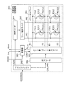
- FIG. 15 is a block diagram showing an example of the configuration of the nonvolatile memory device 300 according to the third embodiment of the present invention.
- the nonvolatile memory device 300 includes a memory cell array 301 including nonvolatile memory elements R311 to R322, an address buffer 302, a control unit 303, a row decoder 304, a word line driver 305, A column decoder 306 and a bit line / plate line driver 307 are provided.
- the bit line / plate line driver 307 includes a sense circuit (sense amplifier), and measures (calculates) a current flowing through the bit line or the plate line, a generated voltage, or a resistance value calculated from the current and the voltage. )can do.
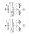
- a write voltage V WRITE that is, a write voltage pulse having a voltage value of ⁇ 2.4 V and a pulse width of 100 ns is output to the plate line with reference to the bit line and applied to the memory cell MC311.
- the writing process is executed by the pulse voltage application unit, and the resistance value of the nonvolatile memory element R311 of the memory cell MC311 changes from the high resistance state to the low resistance state.
- no write voltage pulse is applied to the memory cells MC321 and MC322, and no activation voltage is applied to the gate of the selection transistor T312 of the memory cell MC312. Therefore, the nonvolatile memory elements of the memory cells MC312 and MC321 and MC322 are not applied. The resistance state does not change.
- a new address signal ADDRESS is input to the address buffer 302, and the above-described operation in the write mode of the nonvolatile memory device 300 is repeated for memory cells other than the memory cell MC311. It is.
- the bit line driver 407 sets the bit line selected by the column decoder 406 to the ground state based on the output signal of the column decoder 406.
Landscapes
- Chemical & Material Sciences (AREA)
- Engineering & Computer Science (AREA)
- Materials Engineering (AREA)
- Semiconductor Memories (AREA)
Abstract
Priority Applications (2)
| Application Number | Priority Date | Filing Date | Title |
|---|---|---|---|
| US13/982,280 US9142292B2 (en) | 2011-02-02 | 2012-01-31 | Method for reading data from nonvolatile storage element, and nonvolatile storage device |
| JP2012555748A JP5380611B2 (ja) | 2011-02-02 | 2012-01-31 | 不揮発性記憶素子のデータ読み出し方法及び不揮発性記憶装置 |
Applications Claiming Priority (2)
| Application Number | Priority Date | Filing Date | Title |
|---|---|---|---|
| JP2011-021135 | 2011-02-02 | ||
| JP2011021135 | 2011-02-02 |
Publications (1)
| Publication Number | Publication Date |
|---|---|
| WO2012105232A1 true WO2012105232A1 (fr) | 2012-08-09 |
Family
ID=46602456
Family Applications (1)
| Application Number | Title | Priority Date | Filing Date |
|---|---|---|---|
| PCT/JP2012/000608 Ceased WO2012105232A1 (fr) | 2011-02-02 | 2012-01-31 | Procédé de lecture de données d'élément d'enregistrement non volatil et dispositif d'enregistrement non volatil |
Country Status (3)
| Country | Link |
|---|---|
| US (1) | US9142292B2 (fr) |
| JP (1) | JP5380611B2 (fr) |
| WO (1) | WO2012105232A1 (fr) |
Cited By (1)
| Publication number | Priority date | Publication date | Assignee | Title |
|---|---|---|---|---|
| US9640238B2 (en) | 2014-05-21 | 2017-05-02 | Panasonic Intellectual Property Management Co., Ltd. | Data generating device and data generating method |
Families Citing this family (1)
| Publication number | Priority date | Publication date | Assignee | Title |
|---|---|---|---|---|
| FR3066309B1 (fr) * | 2017-05-09 | 2020-10-16 | Commissariat Energie Atomique | Procede de gestion de l'endurance d'une memoire reinscriptible non volatile et dispositif de programmation d'une telle memoire |
Citations (2)
| Publication number | Priority date | Publication date | Assignee | Title |
|---|---|---|---|---|
| JP2007164969A (ja) * | 2005-12-15 | 2007-06-28 | Samsung Electronics Co Ltd | 選択された基準メモリセルを具備する抵抗型メモリ素子 |
| WO2010058569A1 (fr) * | 2008-11-19 | 2010-05-27 | パナソニック株式会社 | Elément de mémoire non volatile et dispositif de mémoire non volatile |
Family Cites Families (11)
| Publication number | Priority date | Publication date | Assignee | Title |
|---|---|---|---|---|
| US7235407B2 (en) | 2004-05-27 | 2007-06-26 | Sharp Laboratories Of America, Inc. | System and method for forming a bipolar switching PCMO film |
| KR100593750B1 (ko) | 2004-11-10 | 2006-06-28 | 삼성전자주식회사 | 이성분계 금속 산화막을 데이터 저장 물질막으로 채택하는교차점 비휘발성 기억소자 및 그 제조방법 |
| JP3845734B2 (ja) | 2004-11-16 | 2006-11-15 | 国立大学法人金沢大学 | 不揮発性メモリ |
| KR100735750B1 (ko) | 2005-12-15 | 2007-07-06 | 삼성전자주식회사 | 복수개의 균일한 기준 데이터들을 생성하는 기준 셀 블록및 감지증폭 유니트들을 구비하는 반도체 소자들 및 이를채택하는 시스템들 |
| JP4987616B2 (ja) * | 2006-08-31 | 2012-07-25 | 株式会社東芝 | 磁気ランダムアクセスメモリ及び抵抗ランダムアクセスメモリ |
| JP2008065953A (ja) | 2006-09-11 | 2008-03-21 | Fujitsu Ltd | 不揮発性半導体記憶装置及びその読み出し方法 |
| EP2077580B1 (fr) | 2006-11-17 | 2011-11-30 | Panasonic Corporation | Élément de mémoire non volatile, dispositif de mémoire non volatile, dispositif semi-conducteur non volatile et procédé de fabrication d'un élément de mémoire non volatile |
| JP2009021524A (ja) | 2007-07-13 | 2009-01-29 | Panasonic Corp | 抵抗変化素子とその製造方法ならびに抵抗変化型メモリ |
| JP4203532B2 (ja) | 2008-02-04 | 2009-01-07 | シャープ株式会社 | 不揮発性半導体記憶装置及びその書き換え方法 |
| CN102568582A (zh) * | 2010-12-24 | 2012-07-11 | 三星电子株式会社 | 可变电阻器件、包括可变电阻器件的半导体器件及操作方法 |
| JP5966150B2 (ja) * | 2012-07-31 | 2016-08-10 | パナソニックIpマネジメント株式会社 | 不揮発性記憶素子の駆動方法及び不揮発性記憶装置 |
-
2012
- 2012-01-31 WO PCT/JP2012/000608 patent/WO2012105232A1/fr not_active Ceased
- 2012-01-31 JP JP2012555748A patent/JP5380611B2/ja active Active
- 2012-01-31 US US13/982,280 patent/US9142292B2/en active Active
Patent Citations (2)
| Publication number | Priority date | Publication date | Assignee | Title |
|---|---|---|---|---|
| JP2007164969A (ja) * | 2005-12-15 | 2007-06-28 | Samsung Electronics Co Ltd | 選択された基準メモリセルを具備する抵抗型メモリ素子 |
| WO2010058569A1 (fr) * | 2008-11-19 | 2010-05-27 | パナソニック株式会社 | Elément de mémoire non volatile et dispositif de mémoire non volatile |
Cited By (1)
| Publication number | Priority date | Publication date | Assignee | Title |
|---|---|---|---|---|
| US9640238B2 (en) | 2014-05-21 | 2017-05-02 | Panasonic Intellectual Property Management Co., Ltd. | Data generating device and data generating method |
Also Published As
| Publication number | Publication date |
|---|---|
| JP5380611B2 (ja) | 2014-01-08 |
| US9142292B2 (en) | 2015-09-22 |
| JPWO2012105232A1 (ja) | 2014-07-03 |
| US20130308371A1 (en) | 2013-11-21 |
Similar Documents
| Publication | Publication Date | Title |
|---|---|---|
| JP5133471B2 (ja) | 抵抗変化型不揮発性素子の書き込み方法および記憶装置 | |
| JP5966150B2 (ja) | 不揮発性記憶素子の駆動方法及び不揮発性記憶装置 | |
| CN103052991B (zh) | 电阻变化型非易失性存储元件的写入方法 | |
| US8942025B2 (en) | Variable resistance nonvolatile memory element writing method | |
| US9202565B2 (en) | Write method for writing to variable resistance nonvolatile memory element and variable resistance nonvolatile memory device | |
| JP5390730B2 (ja) | 不揮発性記憶素子のデータ書き込み方法及び不揮発性記憶装置 | |
| JP5450911B2 (ja) | 不揮発性記憶素子のデータ読み出し方法及び不揮発性記憶装置 | |
| WO2013080499A1 (fr) | Procédé d'écriture d'élément de stockage non volatil de type à changement de résistance, et dispositif de stockage non volatil de type à changement de résistance | |
| CN102612716B (zh) | 非易失性存储装置 | |
| JP5380611B2 (ja) | 不揮発性記憶素子のデータ読み出し方法及び不揮発性記憶装置 | |
| JP5431267B2 (ja) | 抵抗変化素子の駆動方法及び不揮発性記憶装置 | |
| JP2012169000A (ja) | 抵抗変化素子の駆動方法、不揮発性記憶装置、抵抗変化素子および多値記憶方法 |
Legal Events
| Date | Code | Title | Description |
|---|---|---|---|
| 121 | Ep: the epo has been informed by wipo that ep was designated in this application |
Ref document number: 12741878 Country of ref document: EP Kind code of ref document: A1 |
|
| ENP | Entry into the national phase |
Ref document number: 2012555748 Country of ref document: JP Kind code of ref document: A |
|
| WWE | Wipo information: entry into national phase |
Ref document number: 13982280 Country of ref document: US |
|
| NENP | Non-entry into the national phase |
Ref country code: DE |
|
| 122 | Ep: pct application non-entry in european phase |
Ref document number: 12741878 Country of ref document: EP Kind code of ref document: A1 |