WO2012105508A1 - Ébauche de masque réfléchissante pour la lithographie aux uve - Google Patents
Ébauche de masque réfléchissante pour la lithographie aux uve Download PDFInfo
- Publication number
- WO2012105508A1 WO2012105508A1 PCT/JP2012/052012 JP2012052012W WO2012105508A1 WO 2012105508 A1 WO2012105508 A1 WO 2012105508A1 JP 2012052012 W JP2012052012 W JP 2012052012W WO 2012105508 A1 WO2012105508 A1 WO 2012105508A1
- Authority
- WO
- WIPO (PCT)
- Prior art keywords
- layer
- hard mask
- film
- reflective
- euv
- Prior art date
- Legal status (The legal status is an assumption and is not a legal conclusion. Google has not performed a legal analysis and makes no representation as to the accuracy of the status listed.)
- Ceased
Links
Images


Classifications
-
- G—PHYSICS
- G03—PHOTOGRAPHY; CINEMATOGRAPHY; ANALOGOUS TECHNIQUES USING WAVES OTHER THAN OPTICAL WAVES; ELECTROGRAPHY; HOLOGRAPHY
- G03F—PHOTOMECHANICAL PRODUCTION OF TEXTURED OR PATTERNED SURFACES, e.g. FOR PRINTING, FOR PROCESSING OF SEMICONDUCTOR DEVICES; MATERIALS THEREFOR; ORIGINALS THEREFOR; APPARATUS SPECIALLY ADAPTED THEREFOR
- G03F1/00—Originals for photomechanical production of textured or patterned surfaces, e.g., masks, photo-masks, reticles; Mask blanks or pellicles therefor; Containers specially adapted therefor; Preparation thereof
- G03F1/22—Masks or mask blanks for imaging by radiation of 100nm or shorter wavelength, e.g. X-ray masks, extreme ultraviolet [EUV] masks; Preparation thereof
- G03F1/24—Reflection masks; Preparation thereof
-
- G—PHYSICS
- G03—PHOTOGRAPHY; CINEMATOGRAPHY; ANALOGOUS TECHNIQUES USING WAVES OTHER THAN OPTICAL WAVES; ELECTROGRAPHY; HOLOGRAPHY
- G03F—PHOTOMECHANICAL PRODUCTION OF TEXTURED OR PATTERNED SURFACES, e.g. FOR PRINTING, FOR PROCESSING OF SEMICONDUCTOR DEVICES; MATERIALS THEREFOR; ORIGINALS THEREFOR; APPARATUS SPECIALLY ADAPTED THEREFOR
- G03F1/00—Originals for photomechanical production of textured or patterned surfaces, e.g., masks, photo-masks, reticles; Mask blanks or pellicles therefor; Containers specially adapted therefor; Preparation thereof
- G03F1/54—Absorbers, e.g. of opaque materials
-
- G—PHYSICS
- G03—PHOTOGRAPHY; CINEMATOGRAPHY; ANALOGOUS TECHNIQUES USING WAVES OTHER THAN OPTICAL WAVES; ELECTROGRAPHY; HOLOGRAPHY
- G03F—PHOTOMECHANICAL PRODUCTION OF TEXTURED OR PATTERNED SURFACES, e.g. FOR PRINTING, FOR PROCESSING OF SEMICONDUCTOR DEVICES; MATERIALS THEREFOR; ORIGINALS THEREFOR; APPARATUS SPECIALLY ADAPTED THEREFOR
- G03F1/00—Originals for photomechanical production of textured or patterned surfaces, e.g., masks, photo-masks, reticles; Mask blanks or pellicles therefor; Containers specially adapted therefor; Preparation thereof
- G03F1/68—Preparation processes not covered by groups G03F1/20 - G03F1/50
- G03F1/80—Etching
-
- H—ELECTRICITY
- H10—SEMICONDUCTOR DEVICES; ELECTRIC SOLID-STATE DEVICES NOT OTHERWISE PROVIDED FOR
- H10P—GENERIC PROCESSES OR APPARATUS FOR THE MANUFACTURE OR TREATMENT OF DEVICES COVERED BY CLASS H10
- H10P76/00—Manufacture or treatment of masks on semiconductor bodies, e.g. by lithography or photolithography
- H10P76/20—Manufacture or treatment of masks on semiconductor bodies, e.g. by lithography or photolithography of masks comprising organic materials
- H10P76/204—Manufacture or treatment of masks on semiconductor bodies, e.g. by lithography or photolithography of masks comprising organic materials of organic photoresist masks
- H10P76/2041—Photolithographic processes
Definitions
- the present invention relates to a reflective mask blank for EUV (Extreme Ultra Violet) lithography (hereinafter, also referred to as “EUV mask blank” in the present specification) used in semiconductor manufacturing and the like.
- EUV mask blank Extreme Ultra Violet
- the resolution limit of the pattern is about 1 ⁇ 2 of the exposure wavelength, and it is said that the immersion wavelength is about 1 ⁇ 4 of the exposure wavelength, and the ArF laser (wavelength: 193 nm) is used. Even if the immersion method is used, the exposure wavelength is expected to be about 45 nm.
- EUV lithography which is an exposure technique using EUV light having a wavelength shorter than that of an ArF laser, is promising as a next-generation exposure technique using a wavelength shorter than 45 nm.
- EUV light refers to light having a wavelength in the soft X-ray region or the vacuum ultraviolet region, and specifically refers to light having a wavelength of about 10 to 20 nm, particularly about 13.5 nm ⁇ 0.3 nm.
- EUV light is easily absorbed by any substance, and the refractive index of the substance is close to 1 at this wavelength, so that a conventional refractive optical system such as photolithography using visible light or ultraviolet light cannot be used.
- a reflective optical system that is, a reflective photomask and a mirror are used.
- the mask blank is a layered body before patterning used for manufacturing a photomask.
- the EUV mask blank has a structure in which a reflective layer that reflects EUV light and an absorption layer that absorbs EUV light are formed in this order on a substrate such as glass.
- a low reflection layer for a pattern inspection wavelength (190 to 260 nm) is formed as necessary.
- a material having a high absorption coefficient for EUV light specifically, a material mainly composed of Ta, for example, is used.
- a material having low reflection characteristics with respect to the pattern inspection wavelength specifically, a material mainly containing Ta and O is used.
- a resist film is applied to the uppermost layer of the mask blank (absorbing layer, or the low reflecting layer if a low reflecting layer is formed on the absorbing layer).
- the A pattern is formed on the resist film using an electron beam drawing machine, and then the resist film on which the pattern is formed is used as a mask to undergo an etching process, whereby the pattern is reduced to an absorption layer (on the absorption layer).
- a reflective layer is formed, it is transferred to an absorbing layer and a low reflective layer.
- the film thickness of the resist film must be sufficiently thick.
- the thickness of the resist is usually about 150 nm.
- a layer of a material having resistance to etching conditions of an absorption layer in the case where a low reflection layer is formed on the absorption layer, the absorption layer and the low reflection layer
- the resist can be thinned by providing the (hard mask layer) on the absorption layer (or on the low reflection layer when the low reflection layer is formed on the absorption layer) (Patent Document 1, Patent Document). 2).
- the absorption layer low reflection on the absorption layer
- the etching selectivity between the absorption layer and the low reflection layer and the hard mask layer specifically, the absorption layer (when the low reflection layer is formed on the absorption layer, the absorption layer and The etching rate of the absorption layer under the etching conditions of the low reflection layer (if the low reflection layer is formed on the absorption layer, the etching rate of the absorption layer and the low reflection layer) and the etching rate of the hard mask layer
- the resist can be thinned.
- Patent Document 1 since it has high etching resistance with respect to the fluorine-type gas plasma used for the etching of the light absorption layer (absorption layer) which has Ta as a main component, and it can etch easily by chlorine-type gas plasma, A material mainly composed of chromium (Cr), zirconium (Zr) or indium (In) is considered preferable as a constituent material of the hard mask layer.
- Patent Document 2 since a high etching resistance is exhibited in a fluorine-based dry etching process, a layer containing any one of silicon, oxygen, carbon, and chromium is preferable as the hard mask layer.
- a hard mask layer made of a material that increases the etching selectivity under the etching conditions of the absorption layer is provided on the absorption layer (or on the low reflection layer when a low reflection layer is formed on the absorption layer).
- the resist can be thinned.
- the hard mask layer has a high etching selectivity ratio under the etching conditions of the absorption layer, and the properties of the hard mask layer, specifically, The inventors of the present application have found that the crystal state of the hard mask layer (that is, whether it is a film having a crystal structure or an amorphous film) and the surface roughness are also important.
- the hard mask layer when the hard mask layer is a film having a crystal structure or a film having a large surface roughness, it is predicted that the line edge roughness after pattern formation becomes large and a high-resolution pattern cannot be obtained. For this reason, the inventors of the present application have found that the hard mask layer preferably has a high etching selectivity under the etching conditions of the absorption layer, an amorphous crystal state, and a sufficiently small surface roughness.
- the hard mask layer that is, the main component constituting the hard mask layer, but there is no description regarding the crystal state and surface roughness of the hard mask layer. Points are not taken into account.
- the hard mask layer may be a film having a crystal structure or a film having a large surface roughness. It is possible to become.
- the present invention has a sufficiently high etching selectivity in the etching conditions of the absorption layer or the absorption layer and the low reflection layer, and increases the line edge roughness after pattern formation.
- An object of the present invention is to provide an EUV mask blank capable of obtaining a high-resolution pattern.
- a mask blank having an absorption layer mainly composed of at least one of tantalum (Ta) and palladium (Pd), or the tantalum (Ta) And a low reflection layer mainly comprising at least one of tantalum (Ta) and palladium (Pd) and oxygen (O) on the absorption layer mainly comprising at least one of palladium (Pd).
- a hard mask layer formed on the absorption layer (on the low reflection layer when a low reflection layer is formed on the absorption layer), Cr, one of N and O, H and a film containing a specific ratio (CrNH film or CrOH film), the etching selectivity in the etching conditions of the absorption layer is sufficiently high, One, the crystalline state becomes amorphous, found that the surface roughness can be sufficiently reduced.
- the present invention has been made on the basis of the above findings, and a reflective layer that reflects EUV light, an absorption layer that absorbs EUV light, and a hard mask layer are formed in this order on a substrate.
- a reflective mask blank for EUV lithography The absorption layer is mainly composed of at least one of tantalum (Ta) and palladium (Pd),
- the hard mask layer contains chromium (Cr), nitrogen (N) and hydrogen (H);
- Cr chromium
- N nitrogen
- H hydrogen
- the total content of Cr and N is 85 to 99.9 atomic% (hereinafter, atomic% is referred to as at%), and the content of H is 0.1 to 15 at%.
- a reflective mask blank for EUV lithography is provided.
- the present invention provides a reflective layer that reflects EUV light, an absorption layer that absorbs EUV light, a low reflective layer for mask pattern inspection light (wavelength 190 to 260 nm), a hard mask layer, Is a reflective mask blank for EUV lithography formed in this order,
- the absorption layer is mainly composed of at least one of tantalum (Ta) and palladium (Pd)
- the low reflection layer is mainly composed of at least one of tantalum (Ta) and palladium (Pd) and oxygen (O)
- the hard mask layer contains chromium (Cr), nitrogen (N) and hydrogen (H);
- a reflective mask blank for EUV lithography wherein the total content of Cr and N in the hard mask layer is 85 to 99.9 at% and the content of H is 0.1 to 15 at% To do.
- the hard mask layer containing Cr, N, and H includes at least one selected from the group consisting of helium (He), argon (Ar), neon (Ne), krypton (Kr), and xenon (Xe). It is preferably formed by performing a sputtering method using a Cr target in an atmosphere containing an inert gas, nitrogen (N 2 ), and hydrogen (H 2 ).
- the present invention is a reflective mask blank for EUV lithography in which a reflective layer that reflects EUV light, an absorption layer that absorbs EUV light, and a hard mask layer are formed in this order on a substrate.
- the absorption layer is mainly composed of at least one of tantalum (Ta) and palladium (Pd)
- the hard mask layer contains chromium (Cr), oxygen (O) and hydrogen (H);
- a reflective mask blank for EUV lithography wherein the total content of Cr and O in the hard mask layer is 85 to 99.9 at% and the content of H is 0.1 to 15 at% To do.
- the present invention provides a reflective layer that reflects EUV light, an absorption layer that absorbs EUV light, a low reflective layer for mask pattern inspection light (wavelength 190 to 260 nm), a hard mask layer, Is a reflective mask blank for EUV lithography formed in this order,
- the absorption layer is mainly composed of at least one of tantalum (Ta) and palladium (Pd)
- the low reflection layer is mainly composed of at least one of tantalum (Ta) and palladium (Pd) and oxygen (O)
- the hard mask layer contains chromium (Cr), oxygen (O) and hydrogen (H);
- a reflective mask blank for EUV lithography wherein the total content of Cr and O in the hard mask layer is 85 to 99.9 at% and the content of H is 0.1 to 15 at% To do.
- the hard mask layer containing Cr, O, and H includes at least one selected from the group consisting of helium (He), argon (Ar), neon (Ne), krypton (Kr), and xenon (Xe). It is preferably formed by performing a sputtering method using a Cr target in an atmosphere containing an inert gas, oxygen (O 2 ), and hydrogen (H 2 ).
- the crystal state of the hard mask layer is amorphous.
- the surface roughness (rms) of the surface of the hard mask layer is preferably 0.5 nm or less.
- the hard mask layer preferably has a thickness of 2 to 30 nm.
- a protective layer for protecting the reflective layer may be formed between the reflective layer and the absorbent layer when forming a pattern on the absorbent layer.
- the protective layer is formed of at least one selected from the group consisting of Ru, Ru compound, SiO 2 and Cr compound.
- the etching selectivity in the etching conditions of the absorption layer or the absorption layer and the low reflection layer is sufficiently high, so that the resist thinning required when obtaining a high-resolution pattern can be achieved. Further, since the crystal state of the hard mask layer is amorphous and the surface roughness is sufficiently small, the line edge roughness after pattern formation does not increase and a high resolution pattern can be obtained.
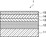
- FIG. 1 is a schematic cross-sectional view showing an embodiment of the EUV mask blank of the present invention.
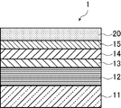
- FIG. 2 is a diagram showing a procedure for forming a pattern on the EUV mask blank 1 shown in FIG. 1 and shows a state in which a resist film 20 is formed on the hard mask layer 15 of the EUV mask blank 1.
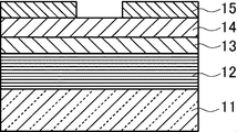
- FIG. 3 is a diagram showing a procedure following FIG. 2 and shows a state in which a pattern is formed on the resist film 20.
- FIG. 4 is a diagram showing a procedure following FIG. 3 and shows a state in which a pattern is formed on the hard mask layer 15.
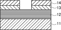
- FIG. 5 is a diagram showing a procedure following FIG. 4, and shows a state where patterns are formed on the absorption layer 13 and the low reflection layer 14.
- FIG. 6 is a diagram showing a procedure following FIG. 5 and shows a state where the hard mask layer 15 is removed.
- FIG. 1 is a schematic cross-sectional view showing an embodiment of the EUV mask blank of the present invention.
- a mask blank 1 shown in FIG. 1 includes a reflection layer 12 that reflects EUV light on a substrate 11, an absorption layer 13 that absorbs EUV light, a low reflection layer 14 in inspection light used for inspection of a mask pattern, The mask layer 15 is formed in this order.
- the EUV mask blank of the present invention in the configuration shown in FIG. 1, only the substrate 11, the reflective layer 12, the absorption layer 13, and the hard mask layer 15 are essential, and the low reflective layer 14 is an optional component.
- a protective layer may be formed between the reflective layer 12 and the absorption layer 13.
- the protective layer referred to here is a layer provided for the purpose of protecting the reflective layer 12 during pattern formation of the absorption layer (in the case of the illustrated EUV mask blank 1, the absorption layer 13 and the low reflection layer 14).
- the absorption layer in the case of the illustrated EUV mask blank 1, the absorption layer 13 and the low reflection layer 14.
- the substrate 11 is required to satisfy the characteristics as a substrate for an EUV mask blank. Therefore, the substrate 11 is required to have a low thermal expansion coefficient.
- the thermal expansion coefficient at 20 ° C. is preferably 0 ⁇ 0.05 ⁇ 10 ⁇ 7 / ° C., and in particular, 0 ⁇ 0. 0.03 ⁇ 10 ⁇ 7 / ° C. is preferable.
- the substrate preferably has excellent smoothness, flatness, and resistance to a cleaning liquid used for cleaning a mask blank or a photomask after pattern formation.
- the substrate 11 is made of glass having a low thermal expansion coefficient, such as SiO 2 —TiO 2 glass, but is not limited to this.
- Crystallized glass, quartz glass, silicon or the like on which ⁇ quartz solid solution is precipitated is used.
- a substrate such as metal can be used. Since the substrate 11 has a smooth surface with a surface roughness (rms) of 0.15 nm or less and a flatness of 100 nm or less, high reflectivity and transfer accuracy can be obtained in a photomask after pattern formation. Is preferred.
- the size and thickness of the substrate 11 are appropriately determined according to the design value of the mask. In the examples described later, SiO 2 —TiO 2 glass having an outer shape of 6 inches (152 mm) square and a thickness of 0.25 inches (6.3 mm) was used. It is preferable that the surface of the substrate 11 on the side where the reflective layer 12 is formed has no defects.
- the depth of the concave defect and the height of the convex defect are not more than 2 nm so that the phase defect does not occur due to the concave defect and / or the convex defect.
- the full width at half maximum of the size of the defect and the convex defect is preferably 60 nm or less.
- the reflective layer 12 is not particularly limited as long as it has desired characteristics as a reflective layer of an EUV mask blank.
- the characteristic particularly required for the reflective layer 12 is a high EUV light reflectance.
- the maximum value of light reflectance near a wavelength of 13.5 nm is preferably 60% or more, More preferably, it is 65% or more.
- the maximum value of the light reflectance near the wavelength of 13.5 nm is preferably 60% or more, and more preferably 65% or more. preferable.
- the reflective layer 12 can achieve high EUV light reflectance, a multilayer reflective film in which a high refractive layer and a low refractive index layer are alternately laminated a plurality of times is usually used as the reflective layer 12.
- a multilayer reflective film in which a high refractive layer and a low refractive index layer are alternately laminated a plurality of times is usually used as the reflective layer 12.
- Si is widely used for the high refractive index layer
- Mo is widely used for the low refractive index layer. That is, the most common is a Mo / Si multilayer reflective film (a multilayer reflective layer in which Mo layers and Si layers are alternately laminated a plurality of times).
- the multilayer reflective film is not limited to this, for example, Ru / Si multilayer reflective film, Mo / Be multilayer reflective film, Mo compound / Si compound multilayer reflective film, Si / Mo / Ru multilayer reflective film, Si / Mo / A Ru / Mo multilayer reflective film and a Si / Ru / Mo / Ru multilayer reflective film can also be used.
- each layer constituting the multilayer reflective film constituting the reflective layer 12 and the number of repeating units of the layer can be appropriately selected according to the film material used and the EUV light reflectance required for the reflective layer.
- the multilayer reflective film is composed of a Mo layer having a film thickness of 2.3 ⁇ 0.1 nm, A Si layer having a thickness of 4.5 ⁇ 0.1 nm may be stacked so that the number of repeating units is 30 to 60.
- each layer which comprises the multilayer reflective film which comprises the reflective layer 12 so that it may become desired thickness using well-known film-forming methods, such as a magnetron sputtering method and an ion beam sputtering method.
- film-forming methods such as a magnetron sputtering method and an ion beam sputtering method.
- a Mo / Si multilayer reflective film is formed by ion beam sputtering
- an Si target is used as a target and Ar gas (gas pressure 1.3 ⁇ 10 ⁇ 2 Pa to 2.7 ⁇ 10 ⁇ as a sputtering gas). 2 Pa)
- an Si film is formed to have a thickness of 4.5 nm at an ion acceleration voltage of 300 to 1500 V and a film formation rate of 0.03 to 0.30 nm / sec.
- the Mo film is formed by laminating 30 to 60 cycles of the Si film and the Mo film.
- the uppermost layer of the multilayer reflective film forming the reflective layer 12 is preferably a layer made of a material that is not easily oxidized.
- the layer of material that is not easily oxidized functions as a cap layer of the reflective layer 12.
- a Si layer can be exemplified as a specific example of the layer of a material that is hardly oxidized and functions as a cap layer.
- the multilayer reflective film forming the reflective layer 12 is a Mo / Si film
- the uppermost layer can be made to function as a cap layer by forming the uppermost layer as an Si layer. In that case, the thickness of the cap layer is preferably 11 ⁇ 2 nm.
- a protective layer may be formed between the reflective layer 12 and the absorption layer 13.
- the protective layer is provided for the purpose of protecting the reflective layer 12 so that the reflective layer 12 is not damaged by the etching process when the absorption layer 13 is patterned by an etching process, usually a dry etching process. Therefore, as the material of the protective layer, a material that is not easily affected by the etching process of the absorption layer 13, that is, the etching rate is slower than that of the absorption layer 13 and is not easily damaged by this etching process is selected.
- Examples of the material satisfying this condition include Cr, Al, Ta and nitrides thereof, Ru and Ru compounds (RuB, RuSi, etc.), and SiO 2 , Si 3 N 4 , Al 2 O 3 and mixtures thereof. Is done. Among these, Ru and Ru compounds (RuB, RuSi, etc.), CrN and SiO 2 are preferable, and Ru and Ru compounds (RuB, RuSi, etc.) are particularly preferable.
- the thickness of the protective layer is preferably 1 to 60 nm.
- the protective layer is formed using a known film formation method such as a magnetron sputtering method or an ion beam sputtering method.
- a Ru film is formed by magnetron sputtering
- a Ru target is used as a target
- Ar gas gas pressure: 1.0 ⁇ 10 ⁇ 2 Pa to 10 ⁇ 10 ⁇ 1 Pa
- an input voltage is 30 V. It is preferable to form a film at a thickness of 2 to 5 nm at a film thickness of 0.01 to 1500 V and a film formation rate of 0.02 to 1.0 nm / sec.
- the characteristic particularly required for the absorption layer 13 is that the EUV light reflectance is extremely low. Specifically, when the surface of the absorption layer 13 is irradiated with light in the wavelength region of EUV light, the maximum light reflectance near a wavelength of 13.5 nm is preferably 0.5% or less, and 0.1% or less. It is more preferable that In the EUV mask blank 1 of the present invention, even when the surface of the low reflection layer 14 is irradiated with light in the wavelength region of EUV light, the maximum light reflectance near a wavelength of 13.5 nm may be 0.5% or less. Preferably, it is 0.1% or less.
- the absorption layer 13 is made of a material having a high EUV light absorption coefficient.
- a material having at least one of tantalum (Ta) and palladium (Pd) as a main component is used as a material having a high absorption coefficient of EUV light constituting the absorption layer 13.
- at least one of Ta or Pd in the material is 40 at% or more, preferably 50 at% or more. More preferably, it means a material containing 55 at% or more.
- the material may contain both Ta and Pd, and TaPd is exemplified.
- a material mainly composed of at least one of Ta and Pd used for the absorption layer 13 is not only Ta or Pd but also hafnium (Hf), silicon (Si), zirconium (Zr), germanium (Ge), boron (B), It may contain at least one element selected from nitrogen (N) and hydrogen (H).
- the material containing the above elements other than Ta or Pd include, for example, TaN, TaNH, PdN, PdNH, TaPdN, TaPdNH, TaHf, TaHfN, TaBSi, TaBSiH, TaBSiN, TaBSiNH, TaB, TaBH, TaBN, Examples include TaBNH, TaSi, TaSiN, TaGe, TaGeN, TaZr, TaZrN, and the like.
- TaNH is preferable because the crystalline state of the absorption layer becomes amorphous and the surface of the absorption layer is excellent in smoothness.
- TaPd, TaPdN, and TaPdNH are preferable because the absorption layer can be made thin because the crystalline state of the absorption layer is amorphous, the refractive index value is small, and a desired extinction coefficient is obtained. Note that in this specification, when the crystal state is referred to as amorphous, what state is indicated will be described later.
- the absorption layer 13 having the above-described configuration can be formed by performing a known film formation method, for example, a magnetron sputtering method or an ion beam sputtering method.
- a known film formation method for example, a magnetron sputtering method or an ion beam sputtering method.
- a TaNH film is formed as the absorption layer 13 by using a magnetron sputtering method
- a Ta target is used as a target, and a mixed gas of Ar, N 2 and H 2 (H 2 gas concentration 1 to 50 vol%) as a sputtering gas.
- a mixed gas of Ar and N 2 (N 2 gas concentration 1 to 80 vol%, Ar gas concentration 5 to 95 vol%, gas pressure 1.0 ⁇ 10 ⁇ 1 Pa to 50 ⁇ 10 ⁇ 1 Pa) is used.
- N 2 gas concentration 1 to 80 vol%, Ar gas concentration 5 to 95 vol%, gas pressure 1.0 ⁇ 10 ⁇ 1 Pa to 50 ⁇ 10 ⁇ 1 Pa) is used.
- the TaPdN film so as to have a thickness of 20 to 50 nm at an input power of 30 to 1000 W and a film formation rate of 0.5 to 60 nm / min.
- concentration of the inert gas sets it as the same concentration range as above-mentioned Ar gas concentration.
- the absorption layer 13 is preferably set such that the total thickness of the absorption layer 13 and the low reflection layer 14 is 10 to 90 nm, and the total thickness of both is 15 to 87 nm. Is more preferable, and it is more preferable to set the film thickness so that the total film thickness of both is 15 to 85 nm.
- the low reflection layer 14 is composed of a film that exhibits low reflection in the inspection light used for inspection of the mask pattern.
- an inspection machine that normally uses light of about 190 to 260 nm as inspection light is used. That is, the difference in reflectance of light of about 190 to 260 nm, specifically, the surface where the absorbing layer 13 is removed by pattern formation and the surface of the absorbing layer 13 remaining without being removed by pattern formation, It is inspected by the difference in reflectance.
- the former is the surface of the reflective layer 12, and when the protective layer is formed on the reflective layer 12, it is the surface of the protective layer.
- the difference in reflectance between the surface of the reflective layer 12 with respect to the wavelength of the inspection light (the protective layer surface when a protective layer is formed on the reflective layer 12) and the surface of the absorption layer 13 is small, the contrast at the time of inspection Will be worse and accurate inspection will not be possible.
- the absorption layer 13 having the above-described configuration has extremely low EUV light reflectance, and has excellent characteristics as the absorption layer of the EUV mask blank 1, but the light reflectance is not always sufficient when viewed with respect to the wavelength of the inspection light. It's not low. As a result, the difference between the reflectance of the surface of the absorption layer 13 at the wavelength of the inspection light and the reflectance of the surface of the reflective layer 12 (or the surface of the protective layer when a protective layer is formed on the reflective layer 12) is small. Therefore, there is a possibility that sufficient contrast at the time of inspection cannot be obtained. If sufficient contrast at the time of inspection is not obtained, pattern defects cannot be sufficiently determined in mask inspection, and accurate defect inspection cannot be performed.
- the EUV mask blank 1 of the present invention by forming the low reflection layer 14 for the inspection light on the absorption layer 13, the light reflectance at the wavelength of the inspection light becomes extremely low, and the contrast at the time of inspection becomes good.
- the low reflection layer 14 is preferably made of a material whose refractive index at the wavelength of the inspection light is lower than that of the absorption layer 13, and its crystal state is preferably amorphous.
- the EUV mask blank 1 of the present invention as a constituent material of the low reflection layer 14, at least one of tantalum (Ta) and palladium (Pd) and oxygen (O) are main components.
- the material to be used is used.
- at least one of Ta or Pd in the material and O is 40 at% in total content.
- it means a material containing preferably 50 at% or more, more preferably 55 at% or more, and TaO and PdO are exemplified as those containing one of Ta or Pd and O.
- the material may contain both Ta and Pd, and TaPdO is exemplified.
- a material mainly composed of at least one of Ta and Pd used for the low reflection layer 14 and O is hafnium (Hf), silicon (Si), zirconium (Zr), germanium (other than Ta, Pd and O). It may contain at least one element selected from Ge), boron (B), nitrogen (N) and hydrogen (H).
- Specific examples of materials containing at least one of Ta and Pd and the above-described elements other than O include TaON, TaONH, PdON, PdONH, TaPdON, TaPdONH, TaHfO, TaHfON, TaBSiO, TaBSiON, and the like. .
- TaO, TaON, and TaONH are preferable because the crystalline state of the absorption layer becomes amorphous and the surface of the absorption layer is excellent in smoothness.
- TaPdO, TaPdON, and TaPdONH are preferable because the absorption layer can be made thin because the crystalline state of the absorption layer is amorphous, the refractive index is small, and a desired extinction coefficient is obtained. Note that in this specification, when the crystal state is referred to as amorphous, what state is indicated will be described later.
- the total thickness of both is preferably 10 to 90 nm, more preferably 15 to 87 nm, and 15 to 85 nm. Is more preferable.
- the film thickness of the low reflection layer 14 is larger than the film thickness of the absorption layer 13, the EUV light absorption characteristics in the absorption layer 13 may be deteriorated. Therefore, the film thickness of the low reflection layer 14 is absorbed. It is preferable that the thickness of the layer 13 is smaller. For this reason, the film thickness of the low reflection layer 14 is preferably 1 to 20 nm, more preferably 1 to 15 nm, and even more preferably 1 to 10 nm.
- the low reflection layer 14 having the above-described configuration can be formed by performing a known film forming method, for example, a magnetron sputtering method or an ion beam sputtering method.
- a known film forming method for example, a magnetron sputtering method or an ion beam sputtering method.
- a TaONH film is formed as the low reflection layer 14 by using a magnetron sputtering method
- a Ta target is used as a target
- a mixed gas (H 2 gas) of Ar, O 2 , N 2 and H 2 is used as a sputtering gas.
- the low reflection layer 14 on the absorption layer 13 because the wavelength of the pattern inspection light and the wavelength of the EUV light are different. Therefore, when EUV light (near 13.5 nm) is used as the pattern inspection light, it is considered unnecessary to form the low reflection layer 14 on the absorption layer 13.
- the wavelength of the inspection light tends to shift to the short wavelength side as the pattern size becomes smaller, and it is conceivable that it will shift to 193 nm and further to 13.5 nm in the future.
- the wavelength of the inspection light is 193 nm, it may not be necessary to form the low reflection layer 14 on the absorption layer 13.
- the wavelength of the inspection light is 13.5 nm, it is considered unnecessary to form the low reflection layer 14 on the absorption layer 13.
- the hard mask layer 15 is required to have a sufficiently high etching selectivity in the etching conditions of the absorption layer 13 and the low reflection layer 14. In order to achieve this, it is necessary that the hard mask layer 15 has sufficient etching resistance with respect to the etching conditions of the absorption layer 13 and the low reflection layer 14.
- a chlorine-based gas process or a fluorine-based gas process is used for etching an absorption layer or a low reflection layer of an EUV mask blank.
- the low reflection layer 14 of the present invention is mainly composed of at least one of Ta and Pd and O, but generally, in the case of a film containing oxygen, it is resistant to etching with respect to a chlorine-based gas process.
- the absorption layer 13 mainly composed of at least one of Ta and Pd in the present invention can also be easily etched for the fluorine-based gas process.
- the etching characteristics of these layers by the chlorine-based gas process and the fluorine-based gas process are also shown in the examples described later.
- the hard mask layer 15 is preferably chlorine. It is easy to etch by the system gas process, and has high etching resistance to the fluorine system gas process. In this case, by using a fluorine-based gas process for etching the absorption layer 13 and the low reflection layer 14, the etching selectivity in the etching conditions of the absorption layer 13 and the low reflection layer 14 is increased. On the other hand, by using a chlorine-based gas process for etching the hard mask layer 15, the etching selectivity obtained by the following formula is increased, and only the hard mask layer 15 can be selectively etched.
- Etching selectivity (during etching of hard mask layer 15) (Etching rate of hard mask layer 15) / (Etching rate of low reflection layer 14)
- the etching selectivity is preferably 2.0 or more, more preferably 2.5 or more, and further preferably 3.0 or more.
- the low reflection layer 14 is not provided on the TaPdN film as the absorption layer 13, but as shown in Table 1, the TaPdN film has etching resistance against the chlorine-based gas process. .
- etching can be easily performed for a fluorine-based gas process.
- the etching selectivity under the etching conditions of the absorption layer 13 is increased.
- the etching selectivity obtained by the following formula is increased, and only the hard mask layer 15 can be selectively etched.
- Etching selectivity (during etching of hard mask layer 15) (Etching rate of hard mask layer 15) / (Etching rate of absorption layer 13)
- the etching selectivity is preferably 4.0 or more, more preferably 4.5 or more, and further preferably 5.0 or more.
- the hard mask layer 15 is required to be made of a material having a sufficiently high etching resistance with respect to the fluorine-based gas process and a high etching rate with respect to the chlorine-based gas process. It is done.
- the hard mask layer 15 is required to have an amorphous crystal state and a sufficiently small surface roughness.
- the hard mask layer is a crystalline film or a film having a large surface roughness, it is predicted that the line edge roughness after pattern formation becomes large and a high resolution pattern cannot be obtained.
- the hard mask layer 15 is in an amorphous state and the surface roughness is sufficiently small, the line edge roughness after pattern formation does not increase and a high-resolution pattern can be obtained.
- the hard mask layer 15 of the EUV mask blank 1 of the present invention satisfies the above characteristics by containing the elements described below in a specific ratio.
- the first aspect of the hard mask layer 15 is a CrNH film containing chromium (Cr), nitrogen (N) and hydrogen (H).
- the hard mask layer 15 is a CrNH film
- the total content of Cr and N is 85 to 99.9 at%, and the content of H is 0.1 to 15 at%. If the H content is less than 0.1 at%, the crystal state of the CrNH film does not become amorphous, and the surface roughness of the CrNH film may increase. On the other hand, even when the H content is higher than 15 at%, the crystal state of the CrNH film does not become amorphous, and the surface roughness of the CrNH film may increase.
- the H content is more preferably 0.1 to 13 at%, further preferably 0.1 to 10 at%, and 0.1 to 8 at%. It is particularly preferred. Further, the total content of Cr and N is more preferably 87 to 99.9 at%, further preferably 90 to 99.9 at%, and particularly preferably 92 to 99.9 at%.
- the composition ratio (atomic ratio) of Cr and N is preferably 9: 1 to 2.5: 7.5, more preferably 8.5: 1.5 to 2.5: 7.5. A ratio of 8: 2 to 2.5: 7.5 is particularly preferable.
- the second mode of the hard mask layer 15 is a CrOH film containing chromium (Cr), oxygen (O), and hydrogen (H).
- Cr chromium
- O oxygen
- H hydrogen
- the total content of Cr and O is 15 to 99.9 at%, and the content of H is 0.1 to 15 at%. If the H content is less than 0.1 at%, the CrOH film does not have an amorphous structure, and the surface roughness of the CrOH film may increase. On the other hand, even when H is higher than 15 at%, the crystal state of the CrOH film does not become amorphous, and the surface roughness of the CrOH film may increase.
- the H content is more preferably 0.1 to 13 at%, further preferably 0.1 to 10 at%, and 0.1 to 8 at%. It is particularly preferred. Further, the total content of Cr and O is more preferably 87 to 99.9 at%, further preferably 90 to 99.9 at%, and particularly preferably 92 to 99.9 at%.
- the composition ratio (atomic ratio) of Cr and O is preferably 9: 1 to 2.5: 7.5, more preferably 8.5: 1.5 to 2.5: 7.5. A ratio of 8: 2 to 2.5: 7.5 is particularly preferable.
- the crystalline state thereof is amorphous.
- the phrase “crystalline state is amorphous” includes a microcrystalline structure other than an amorphous structure having no crystal structure.
- the hard mask layer 15 CrNH film, CrOH film
- the surface roughness (rms) of the hard mask layer 15 is preferably 0.5 nm or less.
- the surface roughness of the hard mask layer 15 can be measured by using an atomic force microscope (Atomic Force Microscope).
- the hard mask layer 15 When the surface roughness of the hard mask layer 15 is large, the edge roughness of the pattern formed on the hard mask layer 15 increases, and the dimensional accuracy of the pattern deteriorates. Since the influence of edge roughness becomes more prominent as the pattern becomes finer, the hard mask layer 15 is required to have a smooth surface. If the surface roughness (rms) of the hard mask layer 15 is 0.5 nm or less, since the surface of the hard mask layer 15 is sufficiently smooth, there is no possibility that the dimensional accuracy of the pattern is deteriorated due to the influence of edge roughness.
- the surface roughness (rms) of the hard mask layer 15 is more preferably 0.4 nm or less, and further preferably 0.3 nm or less.
- the crystal state of the hard mask layer 15 (CrNH film, CrOH film) can be confirmed by an X-ray diffraction (XRD) method to be amorphous, that is, an amorphous structure or a microcrystalline structure. If the crystal state of the hard mask layer 15 is an amorphous structure or a microcrystalline structure, a sharp peak is not seen in a diffraction peak obtained by XRD measurement.
- XRD X-ray diffraction
- the hard mask layer 15 is a film having a crystal structure
- the edge roughness of the pattern formed on the hard mask layer 15 increases due to the selective etching of only a specific crystal orientation. There is a risk that accuracy may deteriorate. For this reason, it is preferable that the crystal state of the hard mask layer 15 (CrNH film, CrOH film) is amorphous.
- the film thickness of the hard mask layer 15 is preferably 2 to 28 nm, and more preferably 2 to 25 nm.
- the hard mask layer 15 (CrNH film, CrOH film) can be formed by performing a known film forming method, for example, a sputtering method such as a magnetron sputtering method or an ion beam sputtering method.
- a sputtering method such as a magnetron sputtering method or an ion beam sputtering method.
- the hard mask layer 15 (CrNH film, CrOH film) is formed by sputtering, it is selected from the group consisting of helium (He), argon (Ar), neon (Ne), krypton (Kr), and xenon (Xe).
- a sputtering method using a Cr target is performed in an atmosphere containing an inert gas containing at least one kind, oxygen (O 2 ) or nitrogen (N 2 ), and hydrogen (H 2 ) Good.
- the magnetron sputtering method When the magnetron sputtering method is used, specifically, it may be performed under the following film forming conditions.
- Sputtering gas Mixed gas of Ar, N 2 and H 2 (H 2 gas concentration 1 to 50 vol%, preferably 1 to 30 vol%, N 2 gas concentration 1 to 80 vol%, preferably 5 to 75 vol%, Ar gas concentration 5 ⁇ 95 vol%, preferably 10 to 94 vol%, gas pressure 1.0 x 10 -1 Pa to 50 x 10 -1 Pa, preferably 1.0 x 10 -1 Pa to 40 x 10 -1 Pa, more preferably 1.0 ⁇ 10 ⁇ 1 Pa to 30 ⁇ 10 ⁇ 1 Pa.)
- Input power 30 to 3000 W, preferably 100 to 3000 W, more preferably 500 to 3000 W
- Deposition rate 0.5 to 60 nm / min, preferably 1.0 to 45 nm / min, more preferably 1.5 to 30 nm / min
- the EUV mask blank 1 of the present invention is a functional film known in the field of EUV mask blanks in addition to the reflective layer 12, the absorbing layer 13, the low reflective layer 14, the hard mask layer 15, and a protective layer formed as necessary. You may have.
- a functional film for example, as described in Japanese Patent Application Publication No. 2003-501823, a high dielectric material applied to the back side of the substrate in order to promote electrostatic chucking of the substrate.
- a functional coating As a specific example of such a functional film, for example, as described in Japanese Patent Application Publication No. 2003-501823, a high dielectric material applied to the back side of the substrate in order to promote electrostatic chucking of the substrate. A functional coating.
- the back surface of the substrate refers to the surface of the substrate 11 in FIG. 1 opposite to the side on which the reflective layer 12 is formed.
- the electrical conductivity and thickness of the constituent material are selected so that the sheet resistance is 100 ⁇ / ⁇ or less.
- the constituent material of the high dielectric coating can be widely selected from those described in known literature.
- a high dielectric constant coating described in JP-A-2003-501823 specifically, a coating made of silicon, TiN, molybdenum, chromium, or TaSi can be applied.
- the thickness of the high dielectric coating can be, for example, 10 to 1000 nm.
- the high dielectric coating can be formed using a known film forming method, for example, a sputtering method such as a magnetron sputtering method or an ion beam sputtering method, a CVD method, a vacuum evaporation method, or an electrolytic plating method.
- a sputtering method such as a magnetron sputtering method or an ion beam sputtering method
- a CVD method a vacuum evaporation method
- electrolytic plating method electrolytic plating method
- FIG. 2 When forming a pattern on the EUV mask blank of the present invention, as shown in FIG. 2, a resist film 20 is formed on the hard mask layer 15 of the EUV mask blank 1, and as shown in FIG. 3 using an electron beam drawing machine. Then, a pattern is formed on the resist film 20. Next, using the patterned resist film as a mask, a pattern is formed on the hard mask layer 15 as shown in FIG. FIG. 4 shows a state in which the resist film 20 is removed after the pattern formation of the hard mask layer 15. For the pattern formation of the hard mask layer 15, etching by a chlorine-based gas process may be performed.
- a pattern is formed on the absorption layer 13 and the low reflection layer 14 as shown in FIG.
- etching by a fluorine-based gas process may be performed.
- the hard mask layer 15 is removed.
- the hard mask layer 15 may be removed by etching using a chlorine-based gas process.
- Example 1 In this example, the EUV mask blank 1 shown in FIG. 1 was produced. However, a protective layer was formed between the reflective layer 12 and the absorbing layer 13.
- a SiO 2 —TiO 2 glass substrate (outer diameter 6 inches (152 mm) square, thickness 6.3 mm) was used. This glass substrate has a thermal expansion coefficient at 20 ° C. of 0.05 ⁇ 10 ⁇ 7 / ° C., Young's modulus of 67 GPa, Poisson's ratio of 0.17, and specific rigidity of 3.07 ⁇ 10 7 m 2 / s 2 .
- This glass substrate was polished to form a smooth surface with a surface roughness (rms) of 0.15 nm or less and a flatness of 100 nm or less.
- a high dielectric coating having a sheet resistance of 100 ⁇ / ⁇ was applied to the back side of the substrate 11 by depositing a Cr film having a thickness of 100 nm using a magnetron sputtering method.
- the substrate 11 is fixed to a normal electrostatic chuck having a flat plate shape via a formed Cr film, and an Si film and a Mo film are alternately formed on the surface of the substrate 11 by using an ion beam sputtering method.
- Mo / Si having a total thickness of 272 nm ((4.5 nm (Si film) +2.3 nm (Mo film)) ⁇ 40 times) having a Si film in the lowermost layer on the substrate surface side
- a multilayer reflective film (reflective layer 12) was formed.
- a protective layer was formed on the Mo / Si multilayer reflective film (reflective layer 12) by forming a Ru film (film thickness 2.5 nm) using an ion beam sputtering method.
- the deposition conditions for the Si film, the Mo film, and the Ru film are as follows.
- Si film formation conditions Target: Si target (boron doped) Sputtering gas: Ar gas (gas pressure 0.02 Pa) Voltage: 700V Deposition rate: 0.077 nm / sec Film thickness: 4.5nm
- Mo target Sputtering gas Ar gas (gas pressure 0.02 Pa) Voltage: 700V Deposition rate: 0.064 nm / sec Film thickness: 2.3 nm
- Ru target Sputtering gas Ar gas (gas pressure 0.02 Pa) Voltage: 500V Deposition rate: 0.023 nm / sec Film thickness: 2.5nm
- an absorption layer 13 (TaNH film) containing Ta, N and H was formed on the protective layer by using a magnetron sputtering method.
- the film forming conditions of the absorption layer 13 are as follows.
- Target Ta target Sputtering gas: Mixed gas of Ar, N 2 and H 2 (Ar: 89 vol%, N 2 : 8.3 vol%, H 2 : 2.7 vol%, gas pressure: 0.46 Pa)
- Input power 300W
- Deposition rate 1.5 nm / min Film thickness: 70nm
- a low reflection layer 14 (TaONH film) containing Ta, O, N, and H was formed on the absorption layer 13 (TaNH film).
- the film forming conditions of the low reflective layer 14 (TaONH film) are as follows.
- Target Ta target Sputtering gas: Mixed gas of Ar, O 2 , N 2 and H 2 (Ar: 48 vol%, O 2 : 36 vol%, N 2 : 14 vol%, H 2 : 2 vol%, gas pressure: 0.3 Pa )
- a hard mask layer 15 (CrNH film) containing Cr, N, and H is formed on the low reflective layer 14 by using a magnetron sputtering method, whereby the reflective layer 12, the protective layer, The EUV mask blank 1 in which the absorption layer 13, the low reflection layer 14, and the hard mask layer 15 were formed in this order was obtained.
- the conditions for forming the hard mask layer 15 are as follows.
- the following evaluations (1) to (4) were performed on the hard mask layer 15 (CrNH film) of the EUV mask blank 1 obtained by the above procedure.
- (1) Film composition The composition of the hard mask layer 15 (CrNH film) is determined using an X-ray photoelectron spectrometer (manufactured by PERKIN ELEMER-PHI), a secondary ion mass spectrometer (Secondary Ion Mass Spectrometer). (PHI-ATOMIKA) and Rutherford Back Scattering Spectroscopy (Kobe Steel) were used.
- the surface roughness of the hard mask layer 15 was measured with a dynamic force mode using an atomic force microscope (SII, SPI-3800).
- the surface roughness measurement area was 1 ⁇ m ⁇ 1 ⁇ m, and SI-DF40 (manufactured by SII) was used as the cantilever.
- the surface roughness (rms) of the hard mask layer 15 was 0.35 nm.
- Etching characteristics were evaluated by the following method instead of using the EUV mask blank 1 produced by the above procedure.
- An absorption layer 13 (TaNH film), a low reflection layer 14 (TaONH film), and a hard mask layer 15 (CrNH film) are sampled on the sample stage (4-inch quartz substrate) of the RF plasma etching apparatus under the same conditions as above.
- a deposited Si chip (10 mm ⁇ 30 mm) was installed. The sample was subjected to plasma RF etching by the following chlorine-based gas process and fluorine-based process.
- Bias RF 50W Etching time: 120 sec Trigger pressure: 3 Pa Etching pressure: 0.3 Pa Etching gas: Cl 2 / He Gas flow rate (Cl 2 / Ar): 4/16 sccm Distance between electrode substrates: 55 mm
- Bias RF 50W Etching time: 120 sec Trigger pressure: 3Pa Etching pressure: 0.3 Pa Etching gas: CF 4 / He Gas flow rate (CF 4 / He): 4/16 sccm Distance between electrode substrates: 55 mm
- Table 1 shows the results of determining the etching rates of the TaNH film, TaONH film, and CrNH film.
- the CrNH film cannot confirm the amount of film loss after etching, and the etching rate is N.P. D. It was. That is, the CrNH film has high etching resistance to the fluorine-based gas process used for etching the absorption layer 13 (TaNH film) and the low reflection layer 14, and the absorption layer 13 (TaNH film) and the low reflection layer 14 ( The etching selectivity under the etching conditions of the TaONH film is sufficiently high.
- the CrNH film had a sufficiently high etching rate with respect to the chlorine-based gas process used for etching the hard mask layer 15.
- Example 2 an EUV mask blank was produced in the same procedure as in Example 1 except that the hard mask layer 15 was a CrOH film.
- the CrOH film was formed under the following conditions.
- Target Cr target Sputtering gas: Mixed gas of Ar, O 2 and H 2 (Ar: 89 vol%, O 2 : 8.3 vol%, H 2 : 2.7 vol%, gas pressure: 0.46 Pa)
- Input power 2000W Deposition rate: 5.5 nm / min Film thickness: 20nm
- Table 1 shows the results of the etching characteristics measured by the same method as in Example 1.
- the CrOH film cannot confirm the amount of film loss after etching, and the etching rate is N.P. D. It was. That is, the CrOH film has a high etching resistance against the fluorine-based gas process used for etching the absorption layer 13 (TaNH film) and the low reflection layer 14, and the absorption layer 13 (TaNH film) and the low reflection layer 14.
- the etching selectivity in the etching conditions of (TaONH film) is sufficiently high.
- the CrOH film had a sufficiently high etching rate with respect to the chlorine-based gas process used for etching the hard mask layer 15.
- Table 1 shows the etching rate of the TaPdN film measured by the same method as in Example 1.
- the etching rate of the absorption layer 13 (TaPdN film) was 4.0 nm / min.
- the etching selection under the etching conditions of the absorption layer 13 (TaPdN film) is performed. The ratio is high enough.
- the etching selectivity of the CrNH film and the CrOH film with respect to the TaPdN film was calculated based on the following formula.
- Etching selectivity in the case of CrNH film
- Etching selectivity in the case of CrOH film
- the etching selectivity with respect to the TaPdN film calculated from the above is 6.2 in the case of the CrNH film and 18.3 in the case of the CrOH film, and it was confirmed that a sufficient etching selectivity was ensured.
- Comparative Example 1 an EUV mask blank was produced in the same procedure as in Example 1 except that the hard mask layer 15 was a CrN film not containing hydrogen.
- the CrN film was formed under the following conditions.
- Target Cr target Sputtering gas: Mixed gas of Ar and N 2 (Ar: 89 vol%, N 2 : 11 vol%, gas pressure: 0.46 Pa)
- Input power 2000W Deposition rate: 5.5 nm / min Film thickness: 20nm
- the surface roughness of the hard mask layer 15 was measured by the same method as in Example 1, and as a result, the surface roughness (rms) was 0.65 nm.
- the CrN film of this comparative example has a crystal structure and a large surface roughness, it is predicted that the line edge roughness at the time of pattern formation will increase, which is not preferable as a hard mask layer of an EUV mask blank.
- Comparative Example 2 an EUV mask blank was produced in the same procedure as in Example 1 except that the hard mask layer 15 was a CrNH film having a hydrogen content higher than 15 at%.
- the CrNH film was formed under the following conditions.
- Target Cr target Sputtering gas: Mixed gas of Ar, N 2 and H 2 (Ar: 80 vol%, N 2 : 5 vol%, H 2 : 15 vol%, gas pressure: 0.46 Pa)
- Input power 2000W Deposition rate: 4.0 nm / min Film thickness: 20nm
- the film composition of the hard mask layer 15 (CrNH film) of the EUV mask blank obtained by the above procedure was measured by the same method as in Example 1.
- the surface roughness of the hard mask layer 15 was measured by the same method as in Example 1, and as a result, the surface roughness (rms) was 0.70 nm.
- the CrNH film of this comparative example has a crystal structure and a large surface roughness, it is predicted that the line edge roughness at the time of pattern formation will increase, which is not preferable as a hard mask layer of an EUV mask blank.
- Comparative Example 3 an EUV mask blank was produced in the same procedure as in Example 2 except that the hard mask layer 15 was a CrO film not containing hydrogen.
- the CrO film was formed under the following conditions.
- Target Cr target Sputtering gas: Mixed gas of Ar and O 2 (Ar: 89 vol%, O 2 : 11 vol%, gas pressure: 0.46 Pa)
- Input power 2000W Deposition rate: 5.5 nm / min Film thickness: 20nm
- the surface roughness of the hard mask layer 15 was measured by the same method as in Example 1, and as a result, the surface roughness (rms) was 0.65 nm.
- the CrO film of this comparative example has a crystal structure and a large surface roughness, it is predicted that the line edge roughness at the time of pattern formation will increase, which is not preferable as a hard mask layer of an EUV mask blank.
- Comparative Example 4 an EUV mask blank was produced in the same procedure as in Example 1 except that the hard mask layer 15 was a CrOH film having a hydrogen content higher than 15 at%.
- the CrOH film was formed under the following conditions.
- Target Cr target Sputtering gas: Mixed gas of Ar, O 2 and H 2 (Ar: 80 vol%, O 2 : 5 vol%, H 2 : 15 vol%, gas pressure: 0.46 Pa)
- Input power 2000W Deposition rate: 4.2 nm / min Film thickness: 20nm
- the film composition of the hard mask layer 15 (CrOH film) of the EUV mask blank obtained by the above procedure was measured by the same method as in Example 1.
- the surface roughness of the hard mask layer 15 was measured by the same method as in Example 1, and as a result, the surface roughness (rms) was 0.75 nm.
- the CrOH film of this comparative example has a crystal structure and a large surface roughness, it is predicted that the line edge roughness at the time of pattern formation will increase, which is not preferable as a hard mask layer of an EUV mask blank.
- EUV mask blank 11 Substrate 12: Reflective layer (multilayer reflective film) 13: Absorption layer 14: Low reflection layer 15: Hard mask layer 20: Resist film
Landscapes
- Physics & Mathematics (AREA)
- General Physics & Mathematics (AREA)
- Exposure Of Semiconductors, Excluding Electron Or Ion Beam Exposure (AREA)
- Preparing Plates And Mask In Photomechanical Process (AREA)
Abstract
Priority Applications (3)
| Application Number | Priority Date | Filing Date | Title |
|---|---|---|---|
| KR1020137015772A KR20140004101A (ko) | 2011-02-01 | 2012-01-30 | Euv 리소그래피용 반사형 마스크 블랭크 |
| JP2012555867A JP5971122B2 (ja) | 2011-02-01 | 2012-01-30 | Euvリソグラフィ用反射型マスクブランク |
| US13/956,691 US9097976B2 (en) | 2011-02-01 | 2013-08-01 | Reflective mask blank for EUV lithography |
Applications Claiming Priority (2)
| Application Number | Priority Date | Filing Date | Title |
|---|---|---|---|
| JP2011019391 | 2011-02-01 | ||
| JP2011-019391 | 2011-02-01 |
Related Child Applications (1)
| Application Number | Title | Priority Date | Filing Date |
|---|---|---|---|
| US13/956,691 Continuation US9097976B2 (en) | 2011-02-01 | 2013-08-01 | Reflective mask blank for EUV lithography |
Publications (1)
| Publication Number | Publication Date |
|---|---|
| WO2012105508A1 true WO2012105508A1 (fr) | 2012-08-09 |
Family
ID=46602722
Family Applications (1)
| Application Number | Title | Priority Date | Filing Date |
|---|---|---|---|
| PCT/JP2012/052012 Ceased WO2012105508A1 (fr) | 2011-02-01 | 2012-01-30 | Ébauche de masque réfléchissante pour la lithographie aux uve |
Country Status (4)
| Country | Link |
|---|---|
| US (1) | US9097976B2 (fr) |
| JP (1) | JP5971122B2 (fr) |
| KR (1) | KR20140004101A (fr) |
| WO (1) | WO2012105508A1 (fr) |
Cited By (15)
| Publication number | Priority date | Publication date | Assignee | Title |
|---|---|---|---|---|
| JP2015008265A (ja) * | 2013-05-31 | 2015-01-15 | 旭硝子株式会社 | Euvリソグラフィ用反射型マスクブランク |
| JP2015133514A (ja) * | 2013-08-30 | 2015-07-23 | Hoya株式会社 | 反射型マスクブランク、反射型マスクブランクの製造方法、反射型マスク及び半導体装置の製造方法 |
| JP2015142083A (ja) * | 2014-01-30 | 2015-08-03 | Hoya株式会社 | 反射型マスクブランク、反射型マスクの製造方法、及び半導体装置の製造方法 |
| WO2015141706A1 (fr) * | 2014-03-18 | 2015-09-24 | Hoya株式会社 | Ébauche équipée d'une couche résistante comportant une couche d'accélération de développement |
| KR20160101920A (ko) * | 2013-12-25 | 2016-08-26 | 호야 가부시키가이샤 | 반사형 마스크 블랭크 및 반사형 마스크, 및 반도체 장치의 제조 방법 |
| JP2018173664A (ja) * | 2018-08-01 | 2018-11-08 | Hoya株式会社 | 反射型マスクブランク、反射型マスクの製造方法、及び半導体装置の製造方法 |
| JP2020064307A (ja) * | 2014-07-11 | 2020-04-23 | アプライド マテリアルズ インコーポレイテッドApplied Materials,Incorporated | 吸収体を有する、平坦化された極紫外線リソグラフィブランク及びその製造システム |
| JP2021110952A (ja) * | 2020-01-08 | 2021-08-02 | エスアンドエス テック カンパニー リミテッド | 極紫外線用反射型ブランクマスク及びフォトマスク |
| US20220075256A1 (en) * | 2019-05-21 | 2022-03-10 | AGC Inc. | Reflective mask blank for euv lithography |
| EP4261614A1 (fr) | 2022-04-13 | 2023-10-18 | Shin-Etsu Chemical Co., Ltd. | Ébauche de photomasque réfléchissant, procédé de fabrication de photomasque réfléchissant et photomasque réfléchissant |
| EP4276532A1 (fr) | 2022-05-13 | 2023-11-15 | Shin-Etsu Chemical Co., Ltd. | Ébauche de photomasque réfléchissant et procédé de fabrication de photomasque réfléchissant |
| JP2024516398A (ja) * | 2021-04-28 | 2024-04-15 | アプライド マテリアルズ インコーポレイテッド | マスク材料のプラズマエッチング |
| EP4474904A2 (fr) | 2023-06-06 | 2024-12-11 | Shin-Etsu Chemical Co., Ltd. | Ébauche de photomasque réfléchissant avec un masque dur monocouche ou bicouche et procédé de fabrication d'un photomasque réfléchissant par gravure sèche de l'ébauche de photomasque réfléchissant |
| WO2025192373A1 (fr) * | 2024-03-13 | 2025-09-18 | Agc株式会社 | Ébauche de masque réfléchissant, masque réfléchissant et procédé de fabrication de masque réfléchissant |
| KR20250164715A (ko) | 2023-03-31 | 2025-11-25 | 에이지씨 가부시키가이샤 | 반사형 마스크 블랭크, 반사형 마스크 블랭크의 제조 방법, 반사형 마스크, 반사형 마스크의 제조 방법 |
Families Citing this family (8)
| Publication number | Priority date | Publication date | Assignee | Title |
|---|---|---|---|---|
| JPWO2013077430A1 (ja) | 2011-11-25 | 2015-04-27 | 旭硝子株式会社 | Euvリソグラフィ用反射型マスクブランクおよびその製造方法 |
| JP2016057577A (ja) * | 2014-09-12 | 2016-04-21 | 信越化学工業株式会社 | フォトマスクブランク |
| WO2018074512A1 (fr) | 2016-10-21 | 2018-04-26 | Hoya株式会社 | Ébauche de masque réfléchissant, procédé de production de masque réfléchissant et procédé de production de dispositif à semi-conducteurs |
| US10553428B2 (en) * | 2017-08-22 | 2020-02-04 | Taiwan Semiconductor Manufacturing Company, Ltd. | Reflection mode photomask and fabrication method therefore |
| US11086215B2 (en) * | 2017-11-15 | 2021-08-10 | Taiwan Semiconductor Manufacturing Co., Ltd. | Extreme ultraviolet mask with reduced mask shadowing effect and method of manufacturing the same |
| JP7250511B2 (ja) * | 2018-12-27 | 2023-04-03 | Hoya株式会社 | 反射型マスクブランク、反射型マスク、及び半導体装置の製造方法 |
| JP7346088B2 (ja) * | 2019-05-31 | 2023-09-19 | 株式会社トッパンフォトマスク | 反射型フォトマスクブランクス及び反射型フォトマスク |
| US11619875B2 (en) * | 2020-06-29 | 2023-04-04 | Taiwan Semiconductor Manufacturing Co., Ltd. | EUV photo masks and manufacturing method thereof |
Citations (5)
| Publication number | Priority date | Publication date | Assignee | Title |
|---|---|---|---|---|
| JP2007250613A (ja) * | 2006-03-14 | 2007-09-27 | Toppan Printing Co Ltd | 反射型マスクブランク、反射型マスク及び極端紫外線の露光方法 |
| JP2008072127A (ja) * | 2006-09-15 | 2008-03-27 | Applied Materials Inc | 極紫外線(euv)フォトマスクのエッチング方法 |
| JP2008078551A (ja) * | 2006-09-25 | 2008-04-03 | Toppan Printing Co Ltd | 反射型フォトマスクブランク及び反射型フォトマスク並びに半導体装置の製造方法 |
| JP2009021582A (ja) * | 2007-06-22 | 2009-01-29 | Advanced Mask Technology Center Gmbh & Co Kg | マスクブランク、フォトマスク、及びフォトマスクの製造方法 |
| JP2009054899A (ja) * | 2007-08-29 | 2009-03-12 | Toppan Printing Co Ltd | 反射型フォトマスクブランク及び反射型フォトマスクの製造方法 |
Family Cites Families (25)
| Publication number | Priority date | Publication date | Assignee | Title |
|---|---|---|---|---|
| JPH10198023A (ja) * | 1997-01-09 | 1998-07-31 | Nec Corp | X線露光マスク及びその製造方法 |
| EP2317383A3 (fr) | 2002-04-11 | 2011-12-28 | HOYA Corporation | Ébauche de masque réfléchissant, masque réfléchissant et procédés de fabrication de l'ébauche de masque et masque |
| JP4483355B2 (ja) | 2004-03-16 | 2010-06-16 | 凸版印刷株式会社 | 極限紫外線露光用マスクブランク及びマスク並びに転写方法 |
| EP1791168A1 (fr) | 2004-09-17 | 2007-05-30 | Asahi Glass Company, Limited | Ébauche de masque réfléchissant pour lithographie euv et procédé de fabrication de ladite ébauche |
| JP4926521B2 (ja) | 2006-03-30 | 2012-05-09 | Hoya株式会社 | 反射型マスクブランクス及び反射型マスク並びに半導体装置の製造方法 |
| TWI444757B (zh) | 2006-04-21 | 2014-07-11 | 旭硝子股份有限公司 | 用於極紫外光(euv)微影術之反射性空白光罩 |
| TWI417647B (zh) | 2006-06-08 | 2013-12-01 | 旭硝子股份有限公司 | Euv微影術用之反射性空白遮光罩及用於彼之具有功能性薄膜的基板 |
| JP2008101246A (ja) | 2006-10-19 | 2008-05-01 | Asahi Glass Co Ltd | Euvリソグラフィ用反射型マスクブランクを製造する際に使用されるスパッタリングターゲット |
| JP5009590B2 (ja) | 2006-11-01 | 2012-08-22 | Hoya株式会社 | マスクブランクの製造方法及びマスクの製造方法 |
| ATE526679T1 (de) | 2006-12-27 | 2011-10-15 | Asahi Glass Co Ltd | Reflexionsmaskenrohling für euv-lithographie |
| JP5018789B2 (ja) | 2007-01-31 | 2012-09-05 | 旭硝子株式会社 | Euvリソグラフィ用反射型マスクブランク |
| JP5040996B2 (ja) | 2007-04-17 | 2012-10-03 | 旭硝子株式会社 | Euvリソグラフィ用反射型マスクブランク |
| JP2009210802A (ja) | 2008-03-04 | 2009-09-17 | Asahi Glass Co Ltd | Euvリソグラフィ用反射型マスクブランク |
| EP2256789B1 (fr) | 2008-03-18 | 2012-07-04 | Asahi Glass Company, Limited | Ébauche de masque réflecteur pour lithographie euv |
| JP5067483B2 (ja) | 2008-06-19 | 2012-11-07 | 旭硝子株式会社 | Euvリソグラフィ用反射型マスクブランク |
| KR20110050427A (ko) | 2008-07-14 | 2011-05-13 | 아사히 가라스 가부시키가이샤 | Euv 리소그래피용 반사형 마스크 블랭크 및 euv 리소그래피용 반사형 마스크 |
| CN102203907B (zh) | 2008-10-30 | 2014-03-26 | 旭硝子株式会社 | Euv光刻用反射型掩模基板 |
| JP5348141B2 (ja) | 2008-10-30 | 2013-11-20 | 旭硝子株式会社 | Euvリソグラフィ用反射型マスクブランク |
| JP5638769B2 (ja) | 2009-02-04 | 2014-12-10 | Hoya株式会社 | 反射型マスクブランクの製造方法及び反射型マスクの製造方法 |
| JP5507876B2 (ja) | 2009-04-15 | 2014-05-28 | Hoya株式会社 | 反射型マスクブランク及び反射型マスクの製造方法 |
| WO2011004850A1 (fr) | 2009-07-08 | 2011-01-13 | 旭硝子株式会社 | Ébauche de masque de type à réflexion pour lithographie par ultraviolet extrême |
| WO2011030521A1 (fr) | 2009-09-09 | 2011-03-17 | Hoya株式会社 | Procédé de fabrication d'une ébauche de masque, procédé de fabrication d'un masque de transfert et procédé de fabrication d'un masque réfléchissant |
| JP5221495B2 (ja) | 2009-11-30 | 2013-06-26 | Hoya株式会社 | マスクブランクの製造方法 |
| KR20130007537A (ko) | 2010-03-02 | 2013-01-18 | 아사히 가라스 가부시키가이샤 | Euv 리소그래피용 반사형 마스크 블랭크 및 그 제조 방법 |
| JP6060636B2 (ja) | 2012-01-30 | 2017-01-18 | 旭硝子株式会社 | Euvリソグラフィ用反射型マスクブランク、および、euvリソグラフィ用反射型マスク |
-
2012
- 2012-01-30 WO PCT/JP2012/052012 patent/WO2012105508A1/fr not_active Ceased
- 2012-01-30 KR KR1020137015772A patent/KR20140004101A/ko not_active Ceased
- 2012-01-30 JP JP2012555867A patent/JP5971122B2/ja active Active
-
2013
- 2013-08-01 US US13/956,691 patent/US9097976B2/en active Active
Patent Citations (5)
| Publication number | Priority date | Publication date | Assignee | Title |
|---|---|---|---|---|
| JP2007250613A (ja) * | 2006-03-14 | 2007-09-27 | Toppan Printing Co Ltd | 反射型マスクブランク、反射型マスク及び極端紫外線の露光方法 |
| JP2008072127A (ja) * | 2006-09-15 | 2008-03-27 | Applied Materials Inc | 極紫外線(euv)フォトマスクのエッチング方法 |
| JP2008078551A (ja) * | 2006-09-25 | 2008-04-03 | Toppan Printing Co Ltd | 反射型フォトマスクブランク及び反射型フォトマスク並びに半導体装置の製造方法 |
| JP2009021582A (ja) * | 2007-06-22 | 2009-01-29 | Advanced Mask Technology Center Gmbh & Co Kg | マスクブランク、フォトマスク、及びフォトマスクの製造方法 |
| JP2009054899A (ja) * | 2007-08-29 | 2009-03-12 | Toppan Printing Co Ltd | 反射型フォトマスクブランク及び反射型フォトマスクの製造方法 |
Cited By (28)
| Publication number | Priority date | Publication date | Assignee | Title |
|---|---|---|---|---|
| JP2015008265A (ja) * | 2013-05-31 | 2015-01-15 | 旭硝子株式会社 | Euvリソグラフィ用反射型マスクブランク |
| JP2015133514A (ja) * | 2013-08-30 | 2015-07-23 | Hoya株式会社 | 反射型マスクブランク、反射型マスクブランクの製造方法、反射型マスク及び半導体装置の製造方法 |
| KR20170121315A (ko) * | 2013-08-30 | 2017-11-01 | 호야 가부시키가이샤 | 반사형 마스크 블랭크, 반사형 마스크 블랭크의 제조방법, 반사형 마스크 및 반도체 장치의 제조방법 |
| KR102012783B1 (ko) | 2013-08-30 | 2019-08-21 | 호야 가부시키가이샤 | 반사형 마스크 블랭크, 반사형 마스크 블랭크의 제조방법, 반사형 마스크 및 반도체 장치의 제조방법 |
| KR102331865B1 (ko) | 2013-12-25 | 2021-11-29 | 호야 가부시키가이샤 | 반사형 마스크 블랭크 및 반사형 마스크, 및 반도체 장치의 제조 방법 |
| KR20160101920A (ko) * | 2013-12-25 | 2016-08-26 | 호야 가부시키가이샤 | 반사형 마스크 블랭크 및 반사형 마스크, 및 반도체 장치의 제조 방법 |
| JP2015142083A (ja) * | 2014-01-30 | 2015-08-03 | Hoya株式会社 | 反射型マスクブランク、反射型マスクの製造方法、及び半導体装置の製造方法 |
| WO2015141706A1 (fr) * | 2014-03-18 | 2015-09-24 | Hoya株式会社 | Ébauche équipée d'une couche résistante comportant une couche d'accélération de développement |
| JP2015194741A (ja) * | 2014-03-18 | 2015-11-05 | Hoya株式会社 | レジスト層付ブランク、その製造方法、マスクブランクおよびインプリント用モールドブランク、ならびに転写用マスク、インプリント用モールドおよびそれらの製造方法 |
| KR20160132979A (ko) | 2014-03-18 | 2016-11-21 | 호야 가부시키가이샤 | 레지스트층을 구비한 블랭크, 그 제조 방법, 마스크 블랭크 및 임프린트용 몰드 블랭크와, 전사용 마스크, 임프린트용 몰드 및 그들의 제조 방법 |
| JP2020064307A (ja) * | 2014-07-11 | 2020-04-23 | アプライド マテリアルズ インコーポレイテッドApplied Materials,Incorporated | 吸収体を有する、平坦化された極紫外線リソグラフィブランク及びその製造システム |
| JP2018173664A (ja) * | 2018-08-01 | 2018-11-08 | Hoya株式会社 | 反射型マスクブランク、反射型マスクの製造方法、及び半導体装置の製造方法 |
| US11982935B2 (en) * | 2019-05-21 | 2024-05-14 | AGC Inc. | Reflective mask blank for EUV lithography |
| US20220075256A1 (en) * | 2019-05-21 | 2022-03-10 | AGC Inc. | Reflective mask blank for euv lithography |
| US11815801B2 (en) | 2020-01-08 | 2023-11-14 | S & S Tech Co., Ltd. | Reflective type blankmask and photomask for EUV |
| JP2021110952A (ja) * | 2020-01-08 | 2021-08-02 | エスアンドエス テック カンパニー リミテッド | 極紫外線用反射型ブランクマスク及びフォトマスク |
| JP7564968B2 (ja) | 2021-04-28 | 2024-10-09 | アプライド マテリアルズ インコーポレイテッド | マスク材料のプラズマエッチング |
| JP2024516398A (ja) * | 2021-04-28 | 2024-04-15 | アプライド マテリアルズ インコーポレイテッド | マスク材料のプラズマエッチング |
| KR20230146998A (ko) | 2022-04-13 | 2023-10-20 | 신에쓰 가가꾸 고교 가부시끼가이샤 | 반사형 포토마스크 블랭크, 반사형 포토마스크의 제조 방법 및 반사형 포토마스크 |
| EP4261614A1 (fr) | 2022-04-13 | 2023-10-18 | Shin-Etsu Chemical Co., Ltd. | Ébauche de photomasque réfléchissant, procédé de fabrication de photomasque réfléchissant et photomasque réfléchissant |
| EP4276532A1 (fr) | 2022-05-13 | 2023-11-15 | Shin-Etsu Chemical Co., Ltd. | Ébauche de photomasque réfléchissant et procédé de fabrication de photomasque réfléchissant |
| KR20230159292A (ko) | 2022-05-13 | 2023-11-21 | 신에쓰 가가꾸 고교 가부시끼가이샤 | 반사형 포토마스크 블랭크, 및 반사형 포토마스크의 제조 방법 |
| JP2023167983A (ja) * | 2022-05-13 | 2023-11-24 | 信越化学工業株式会社 | 反射型フォトマスクブランク、及び反射型フォトマスクの製造方法 |
| JP7687269B2 (ja) | 2022-05-13 | 2025-06-03 | 信越化学工業株式会社 | 反射型フォトマスクブランク、及び反射型フォトマスクの製造方法 |
| KR20250164715A (ko) | 2023-03-31 | 2025-11-25 | 에이지씨 가부시키가이샤 | 반사형 마스크 블랭크, 반사형 마스크 블랭크의 제조 방법, 반사형 마스크, 반사형 마스크의 제조 방법 |
| EP4474904A2 (fr) | 2023-06-06 | 2024-12-11 | Shin-Etsu Chemical Co., Ltd. | Ébauche de photomasque réfléchissant avec un masque dur monocouche ou bicouche et procédé de fabrication d'un photomasque réfléchissant par gravure sèche de l'ébauche de photomasque réfléchissant |
| KR20240173694A (ko) | 2023-06-06 | 2024-12-13 | 신에쓰 가가꾸 고교 가부시끼가이샤 | 반사형 포토마스크 블랭크, 및 반사형 포토마스크의 제조 방법 |
| WO2025192373A1 (fr) * | 2024-03-13 | 2025-09-18 | Agc株式会社 | Ébauche de masque réfléchissant, masque réfléchissant et procédé de fabrication de masque réfléchissant |
Also Published As
| Publication number | Publication date |
|---|---|
| KR20140004101A (ko) | 2014-01-10 |
| US9097976B2 (en) | 2015-08-04 |
| US20130316272A1 (en) | 2013-11-28 |
| JPWO2012105508A1 (ja) | 2014-07-03 |
| JP5971122B2 (ja) | 2016-08-17 |
Similar Documents
| Publication | Publication Date | Title |
|---|---|---|
| JP5971122B2 (ja) | Euvリソグラフィ用反射型マスクブランク | |
| JP5018789B2 (ja) | Euvリソグラフィ用反射型マスクブランク | |
| JP5018787B2 (ja) | Euvリソグラフィ用反射型マスクブランク | |
| JP5590113B2 (ja) | Euvリソグラフィ用反射型マスクブランクおよびその製造方法 | |
| JP6287099B2 (ja) | Euvリソグラフィ用反射型マスクブランク | |
| JP5040996B2 (ja) | Euvリソグラフィ用反射型マスクブランク | |
| KR101335077B1 (ko) | Euv 리소그래피용 반사형 마스크 블랭크 | |
| JP5067483B2 (ja) | Euvリソグラフィ用反射型マスクブランク | |
| JP5708651B2 (ja) | Euvリソグラフィ用反射型マスクブランク | |
| JP5348141B2 (ja) | Euvリソグラフィ用反射型マスクブランク | |
| US8133643B2 (en) | Reflective mask blank for EUV lithography | |
| JP4867695B2 (ja) | Euvリソグラフィ用反射型マスクブランク | |
| JPWO2011004850A1 (ja) | Euvリソグラフィ用反射型マスクブランク | |
| US20220075256A1 (en) | Reflective mask blank for euv lithography | |
| JP5333016B2 (ja) | Euvリソグラフィ用反射型マスクブランク | |
| JP2009210802A (ja) | Euvリソグラフィ用反射型マスクブランク | |
| JP2009252788A (ja) | Euvリソグラフィ用反射型マスクブランク |
Legal Events
| Date | Code | Title | Description |
|---|---|---|---|
| 121 | Ep: the epo has been informed by wipo that ep was designated in this application |
Ref document number: 12742602 Country of ref document: EP Kind code of ref document: A1 |
|
| ENP | Entry into the national phase |
Ref document number: 2012555867 Country of ref document: JP Kind code of ref document: A |
|
| ENP | Entry into the national phase |
Ref document number: 20137015772 Country of ref document: KR Kind code of ref document: A |
|
| NENP | Non-entry into the national phase |
Ref country code: DE |
|
| 122 | Ep: pct application non-entry in european phase |
Ref document number: 12742602 Country of ref document: EP Kind code of ref document: A1 |