WO2012108546A1 - Substrat inoxydable ayant une couche plaquée or et procédé de formation d'un motif partiellement plaqué or sur un substrat inoxydable - Google Patents
Substrat inoxydable ayant une couche plaquée or et procédé de formation d'un motif partiellement plaqué or sur un substrat inoxydable Download PDFInfo
- Publication number
- WO2012108546A1 WO2012108546A1 PCT/JP2012/053443 JP2012053443W WO2012108546A1 WO 2012108546 A1 WO2012108546 A1 WO 2012108546A1 JP 2012053443 W JP2012053443 W JP 2012053443W WO 2012108546 A1 WO2012108546 A1 WO 2012108546A1
- Authority
- WO
- WIPO (PCT)
- Prior art keywords
- stainless steel
- gold plating
- steel substrate
- plating layer
- gold
- Prior art date
- Legal status (The legal status is an assumption and is not a legal conclusion. Google has not performed a legal analysis and makes no representation as to the accuracy of the status listed.)
- Ceased
Links
Images







Classifications
-
- C—CHEMISTRY; METALLURGY
- C25—ELECTROLYTIC OR ELECTROPHORETIC PROCESSES; APPARATUS THEREFOR
- C25D—PROCESSES FOR THE ELECTROLYTIC OR ELECTROPHORETIC PRODUCTION OF COATINGS; ELECTROFORMING; APPARATUS THEREFOR
- C25D5/00—Electroplating characterised by the process; Pretreatment or after-treatment of workpieces
- C25D5/10—Electroplating with more than one layer of the same or of different metals
-
- B—PERFORMING OPERATIONS; TRANSPORTING
- B05—SPRAYING OR ATOMISING IN GENERAL; APPLYING FLUENT MATERIALS TO SURFACES, IN GENERAL
- B05D—PROCESSES FOR APPLYING FLUENT MATERIALS TO SURFACES, IN GENERAL
- B05D3/00—Pretreatment of surfaces to which liquids or other fluent materials are to be applied; After-treatment of applied coatings, e.g. intermediate treating of an applied coating preparatory to subsequent applications of liquids or other fluent materials
- B05D3/10—Pretreatment of surfaces to which liquids or other fluent materials are to be applied; After-treatment of applied coatings, e.g. intermediate treating of an applied coating preparatory to subsequent applications of liquids or other fluent materials by other chemical means
- B05D3/107—Post-treatment of applied coatings
-
- C—CHEMISTRY; METALLURGY
- C23—COATING METALLIC MATERIAL; COATING MATERIAL WITH METALLIC MATERIAL; CHEMICAL SURFACE TREATMENT; DIFFUSION TREATMENT OF METALLIC MATERIAL; COATING BY VACUUM EVAPORATION, BY SPUTTERING, BY ION IMPLANTATION OR BY CHEMICAL VAPOUR DEPOSITION, IN GENERAL; INHIBITING CORROSION OF METALLIC MATERIAL OR INCRUSTATION IN GENERAL
- C23C—COATING METALLIC MATERIAL; COATING MATERIAL WITH METALLIC MATERIAL; SURFACE TREATMENT OF METALLIC MATERIAL BY DIFFUSION INTO THE SURFACE, BY CHEMICAL CONVERSION OR SUBSTITUTION; COATING BY VACUUM EVAPORATION, BY SPUTTERING, BY ION IMPLANTATION OR BY CHEMICAL VAPOUR DEPOSITION, IN GENERAL
- C23C30/00—Coating with metallic material characterised only by the composition of the metallic material, i.e. not characterised by the coating process
-
- C—CHEMISTRY; METALLURGY
- C23—COATING METALLIC MATERIAL; COATING MATERIAL WITH METALLIC MATERIAL; CHEMICAL SURFACE TREATMENT; DIFFUSION TREATMENT OF METALLIC MATERIAL; COATING BY VACUUM EVAPORATION, BY SPUTTERING, BY ION IMPLANTATION OR BY CHEMICAL VAPOUR DEPOSITION, IN GENERAL; INHIBITING CORROSION OF METALLIC MATERIAL OR INCRUSTATION IN GENERAL
- C23F—NON-MECHANICAL REMOVAL OF METALLIC MATERIAL FROM SURFACE; INHIBITING CORROSION OF METALLIC MATERIAL OR INCRUSTATION IN GENERAL; MULTI-STEP PROCESSES FOR SURFACE TREATMENT OF METALLIC MATERIAL INVOLVING AT LEAST ONE PROCESS PROVIDED FOR IN CLASS C23 AND AT LEAST ONE PROCESS COVERED BY SUBCLASS C21D OR C22F OR CLASS C25
- C23F1/00—Etching metallic material by chemical means
- C23F1/44—Compositions for etching metallic material from a metallic material substrate of different composition
-
- C—CHEMISTRY; METALLURGY
- C25—ELECTROLYTIC OR ELECTROPHORETIC PROCESSES; APPARATUS THEREFOR
- C25D—PROCESSES FOR THE ELECTROLYTIC OR ELECTROPHORETIC PRODUCTION OF COATINGS; ELECTROFORMING; APPARATUS THEREFOR
- C25D3/00—Electroplating: Baths therefor
- C25D3/02—Electroplating: Baths therefor from solutions
- C25D3/48—Electroplating: Baths therefor from solutions of gold
-
- C—CHEMISTRY; METALLURGY
- C25—ELECTROLYTIC OR ELECTROPHORETIC PROCESSES; APPARATUS THEREFOR
- C25D—PROCESSES FOR THE ELECTROLYTIC OR ELECTROPHORETIC PRODUCTION OF COATINGS; ELECTROFORMING; APPARATUS THEREFOR
- C25D5/00—Electroplating characterised by the process; Pretreatment or after-treatment of workpieces
- C25D5/02—Electroplating of selected surface areas
- C25D5/022—Electroplating of selected surface areas using masking means
-
- C—CHEMISTRY; METALLURGY
- C25—ELECTROLYTIC OR ELECTROPHORETIC PROCESSES; APPARATUS THEREFOR
- C25D—PROCESSES FOR THE ELECTROLYTIC OR ELECTROPHORETIC PRODUCTION OF COATINGS; ELECTROFORMING; APPARATUS THEREFOR
- C25D5/00—Electroplating characterised by the process; Pretreatment or after-treatment of workpieces
- C25D5/34—Pretreatment of metallic surfaces to be electroplated
- C25D5/36—Pretreatment of metallic surfaces to be electroplated of iron or steel
-
- Y—GENERAL TAGGING OF NEW TECHNOLOGICAL DEVELOPMENTS; GENERAL TAGGING OF CROSS-SECTIONAL TECHNOLOGIES SPANNING OVER SEVERAL SECTIONS OF THE IPC; TECHNICAL SUBJECTS COVERED BY FORMER USPC CROSS-REFERENCE ART COLLECTIONS [XRACs] AND DIGESTS
- Y10—TECHNICAL SUBJECTS COVERED BY FORMER USPC
- Y10T—TECHNICAL SUBJECTS COVERED BY FORMER US CLASSIFICATION
- Y10T428/00—Stock material or miscellaneous articles
- Y10T428/12—All metal or with adjacent metals
- Y10T428/12361—All metal or with adjacent metals having aperture or cut
-
- Y—GENERAL TAGGING OF NEW TECHNOLOGICAL DEVELOPMENTS; GENERAL TAGGING OF CROSS-SECTIONAL TECHNOLOGIES SPANNING OVER SEVERAL SECTIONS OF THE IPC; TECHNICAL SUBJECTS COVERED BY FORMER USPC CROSS-REFERENCE ART COLLECTIONS [XRACs] AND DIGESTS
- Y10—TECHNICAL SUBJECTS COVERED BY FORMER USPC
- Y10T—TECHNICAL SUBJECTS COVERED BY FORMER US CLASSIFICATION
- Y10T428/00—Stock material or miscellaneous articles
- Y10T428/12—All metal or with adjacent metals
- Y10T428/12389—All metal or with adjacent metals having variation in thickness
-
- Y—GENERAL TAGGING OF NEW TECHNOLOGICAL DEVELOPMENTS; GENERAL TAGGING OF CROSS-SECTIONAL TECHNOLOGIES SPANNING OVER SEVERAL SECTIONS OF THE IPC; TECHNICAL SUBJECTS COVERED BY FORMER USPC CROSS-REFERENCE ART COLLECTIONS [XRACs] AND DIGESTS
- Y10—TECHNICAL SUBJECTS COVERED BY FORMER USPC
- Y10T—TECHNICAL SUBJECTS COVERED BY FORMER US CLASSIFICATION
- Y10T428/00—Stock material or miscellaneous articles
- Y10T428/12—All metal or with adjacent metals
- Y10T428/12493—Composite; i.e., plural, adjacent, spatially distinct metal components [e.g., layers, joint, etc.]
- Y10T428/12771—Transition metal-base component
- Y10T428/12861—Group VIII or IB metal-base component
- Y10T428/12889—Au-base component
Definitions
- the present invention relates to a method for directly forming a gold plating pattern on stainless steel, particularly a stainless steel substrate, and a stainless steel substrate having a gold plating layer on a surface different from the main plane.
- stainless steel has been used in various products such as connectors, fuel cells, hard disk suspensions, and ink jets as forms of substrates and the like.
- a desired pattern made of a conductive material such as copper, nickel, silver, or gold is formed on the stainless steel substrate in order to partially enhance the corrosion resistance of the stainless steel substrate or to conduct external connection ( Patent Documents 1 and 2).
- a copper plating layer is formed on a stainless steel substrate as a first layer and a silver plating layer or a nickel plating layer is formed as a second layer to form a pattern
- the passivation present on the surface of the stainless steel substrate There was a problem that sufficient adhesion between the coating and the copper plating layer could not be obtained.
- a nickel plating layer is formed as a first layer on the entire surface of the stainless steel substrate, then a silver plating layer or a gold plating layer is laminated in a desired pattern, and then an unnecessary nickel plating layer is peeled and removed.
- the ionization tendency between the nickel plating layer and the silver plating layer or the gold plating layer regardless of whether the stripping solution used for stripping the nickel plating layer is an alkaline or acidic stripping solution Due to the difference, the silver plating layer or the gold plating layer may be discolored to show erosion. In order to avoid the occurrence of defects due to the erosion of the stripping solution, it is necessary to prevent moisture from being taken in from the outside air.
- the silver plating layer or the gold plating layer is thickened, or the current density is increased to increase the density. It is required to improve.
- the adhesion of the gold plating layer becomes non-uniform or poor adhesion occurs.
- the surface corrosion of the stainless steel substrate occurs when the passivation film is excessively removed.
- a hydrochloric acid-based plating solution used, the surface corrosion action of the stainless steel substrate occurs as a simultaneous action during gold plating, so that the adhesion of the gold plating layer is good.
- the hydrochloric acid concentration of the hydrochloric acid plating solution is increased to increase the plating speed, corrosion occurs and the production efficiency is improved.
- the above problems are problems from the viewpoint of chemical reaction. Furthermore, when there are processing parts such as recess patterns and through holes on the stainless steel substrate, and the surface shape is complicated, or such processing parts are Even if it does not exist, it is desired to form a gold plating layer directly only on a desired portion of the stainless steel substrate and efficiently form the gold plating layer while suppressing the amount of gold used.
- the present invention has been made in view of the above circumstances, and a method for suppressing corrosion on a stainless steel substrate and forming a thin and defect-free gold plating layer pattern directly on a desired portion of the stainless steel substrate, and gold plating It is to provide a stainless steel substrate having a layer.
- a method for forming a partial gold plating pattern on a stainless steel substrate includes a stainless steel having opposing main planes and a processing portion constituted by a surface different from the main plane. After pre-treating the substrate, a first plating step of forming a first gold plating layer on the entire surface of the stainless steel substrate using a hydrochloric acid plating solution, and only on the first gold plating layer covering the processing site. The second plating step of forming a second gold plating layer in a desired pattern by mask plating, and the first gold plating layer in the region where the second gold plating layer does not exist is peeled off using an alkaline stripping solution. And a peeling process.
- the method for forming a partial gold plating pattern on the stainless steel substrate of the present invention is performed after pre-treating a stainless steel substrate having an opposing main plane and a processing portion constituted by a surface different from the main plane, A resist pattern is formed on the stainless steel substrate so that a desired part including at least the processed part is exposed, and then a first gold plating layer is formed on the exposed stainless steel substrate surface using a hydrochloric acid plating solution.
- the first gold plating layer in the region is configured to have a stripping step of stripping and removing using an alkaline stripping solution.
- the mask plating in the second plating step is configured to use a mask having an opening having an area smaller than the projected area of the processed part in a plane parallel to the main plane.
- the resist pattern is formed to be thicker than the thickness of the first gold plating layer to be formed.
- the second plating step a cyan plating solution is used, and the thickness of the first gold plating layer is in the range of 0.010 to 0.15 ⁇ m.
- the configuration was as another aspect of the present invention, in the second plating step, a hydrochloric acid plating solution is used, and the thickness of the first gold plating layer is in the range of 0.015 to 0.15 ⁇ m.
- the pretreatment of the stainless steel substrate in the first plating step includes an alkali cleaning treatment and a hydrochloric acid immersion treatment.
- gold ions are recovered after the first plating step and after the second plating step.
- the second gold plating layer formed in the second plating step is formed thicker than the first gold plating layer formed in the first plating step.
- the method for forming a partial gold plating pattern on a stainless steel substrate according to the present invention is such that after a pretreatment is performed on the stainless steel substrate, a resist pattern is formed so that only a desired portion of the stainless steel substrate is exposed, and then exposed.
- the resist pattern is formed thicker than the thickness of the first gold plating layer to be formed.
- the mask is arranged after the resist pattern formed in the first plating step is peeled and removed.
- the second plating step a cyan plating solution is used, and the thickness of the first gold plating layer is in the range of 0.010 to 0.15 ⁇ m.
- the configuration was as another aspect of the present invention, in the second plating step, a hydrochloric acid plating solution is used, and the thickness of the first gold plating layer is in the range of 0.015 to 0.15 ⁇ m.
- the pretreatment of the stainless steel substrate in the first plating step includes an alkali cleaning treatment and a hydrochloric acid immersion treatment.
- gold ions are recovered after the first plating step and after the second plating step.
- the second gold plating layer formed in the second plating step is formed thicker than the first gold plating layer formed in the first plating step.
- the stainless steel substrate of the present invention is a stainless steel substrate having an opposing main plane and a processing portion constituted by a surface different from the main plane, and the main plane has no gold plating layer, and the processing The gold plating layer was present on the surface of the part.
- the gold plating layer has a thickness in the range of 0.15 to 1 ⁇ m.
- the stainless steel substrate of the present invention is a stainless steel substrate having an opposing main plane and a processing portion constituted by a surface different from the main plane, and a gold plating thin film is formed on at least a part of the main plane.
- the gold plating layer is present on the surface of the processed portion, and the gold plating layer is thicker than the gold plating thin film, and the difference is in the range of 0.15 to 1 ⁇ m.
- the processing site is a recess and / or a through hole.
- the first gold plating layer is formed on the entire surface of the pretreated stainless steel substrate or on a desired site using the hydrochloric acid plating solution. 1 Adhesiveness with a gold plating layer is improved. Also, the second gold plating layer is formed in a desired pattern by mask plating only on the first gold plating layer, and then the first gold plating layer is peeled and removed using an alkaline stripping solution. Erosion is prevented. Moreover, since there is no difference in ionization tendency between the first gold plating layer and the second gold plating layer, the second gold plating layer does not erode and the thickness of the second gold plating layer can be reduced. it can.
- the pattern of the formed gold plating layer is a two-layer structure, both layers are gold plating layers, so that a stable coating without causing a battery reaction between the layers is obtained. Furthermore, when the stainless steel substrate has an unnecessary part of the gold plating layer pattern, this part can be exposed, so even if the stainless steel substrate is processed in advance, use of this processed part is possible. It will not cause any trouble. Moreover, when forming a gold plating layer only in a desired site
- the gold plating layer is present in a processed part constituted by a surface different from the main plane, and the thickness of the stainless steel substrate in the region where the main plane is exposed is set to a desired thickness. Therefore, strength necessary for handling can be maintained in production, work efficiency and efficiency of an automatic device can be increased, and easy handling leads to defect suppression. Further, in the stainless steel substrate of the present invention, the gold plating layer is present in the processing portion constituted by a surface different from the main plane, and the gold plating thin film is present in the main plane, so that the passive film on the stainless steel substrate is re-formed. Can be prevented, the work efficiency and the efficiency of the automatic device can be increased, and the ease of handling leads to defect suppression.
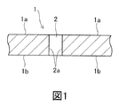
- FIG. 1 is a partial cross-sectional view showing an example of a stainless steel substrate having a processed part.
- FIG. 2 is a partial cross-sectional view showing another example of a stainless steel substrate having a processed part.
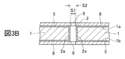
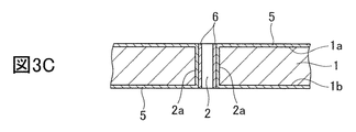
- 3A to 3D are process diagrams for explaining an example of a method for forming a partial gold plating pattern of the present invention.
- 4A to 4D are process diagrams for explaining another example of the method for forming a partial gold plating pattern of the present invention.
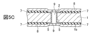
- 5A to 5E are process diagrams for explaining another example of the method for forming a partial gold plating pattern of the present invention.
- FIG. 6 is a diagram for explaining another example of the method for forming a partial gold plating pattern of the present invention.
- FIG. 7 is a view showing an example of a stainless steel substrate having a gold plating layer of the present invention, and is a partial plan view of the stainless steel substrate shown in FIG. 3D.
- FIG. 8 is a view showing another example of the stainless steel substrate having the gold plating layer of the present invention, and is a partial plan view of the stainless steel substrate shown in FIG. 4D.
- FIG. 9 is a cross-sectional view corresponding to FIGS. 3D and 4D showing another example of a stainless steel substrate having a gold plating layer of the present invention.
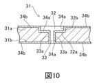
- FIG. 10 is a cross-sectional view corresponding to FIG. 9 showing another example of the stainless steel substrate having the gold plating layer of the present invention.
- FIG. 11 is a partial plan view showing another example of the stainless steel substrate having the gold plating layer of the present invention, and corresponds to the partial plan view of the stainless steel substrate shown in FIG. 5D.
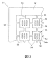
- FIG. 12 is a partial plan view showing another example of the stainless steel substrate having the gold plating layer of the present invention.
- FIG. 1 is a diagram showing an example of a stainless steel substrate having a processed portion.
- the stainless steel substrate 1 has opposing main planes 1a and 1b, and is further configured by a wall surface 2a different from the main planes 1a and 1b.
- the through-hole 2 is provided as a processing site.
- the number, position, size, and shape of the through-hole 2 as a processing part are not limited.
- FIG. 2 is a view showing another example of a stainless steel substrate having a processed part.
- the stainless steel substrate 11 has opposing main planes 11a and 11b, and a bottom surface 12a different from the main plane 11a, It has the recessed part 12 comprised by the wall surface 12b as a process site
- the number, position, size, and shape of the recesses 12 as processing parts are not limited.
- a main plane is a pair of plane which opposes in the thickness direction of a stainless steel substrate in the state before giving processing, such as an etching and press work.
- processing such as an etching and press work.
- first gold plating layers 5 and 15 are directly formed using a liquid (FIGS. 3A and 4A). That is, in the stainless steel substrate 1, the first gold plating layer 5 is formed on the main planes 1 a and 1 b and the wall surface 2 a constituting the through hole 2 that is a processing site. Further, in the stainless steel substrate 11, the first gold plating layer 15 is formed on the main planes 11a and 11b and the bottom surface 12a and the wall surface 12b constituting the recess 12 which is a processing site.
- the pretreatment for the stainless steel substrates 1 and 11 is for the purpose of activating by removing the surface degreasing and the passive film, for example, alkali dipping treatment, alkaline electrolytic treatment, acid electrolytic treatment, acid dipping treatment, etc. It can carry out by selecting suitably from the method.
- the transition time from the pretreatment to the formation of the first gold plating layers 5 and 15 is set to a range in which the passive film is not re-formed on the stainless steel substrates 1 and 11.
- the first gold plating layers 5 and 15 are formed using a hydrochloric acid plating solution.
- the hydrochloric acid plating solution to be used is preferably one that takes into consideration the prevention of erosion of the stainless steel substrates 1 and 11 and the reduction of the plating time.
- a hydrochloric acid plating solution prepared so that the degree of occurrence of micropitting corrosion on the surfaces of the target stainless steel substrates 1 and 11 is 5 or less per unit area (mm 2 ) can be used.
- the micro pitting corrosion is measured by immersing the stainless steel substrate in a hydrochloric acid plating solution for 10 seconds, washing with water and drying, and then observing with a scanning electron microscope.
- a hydrochloric acid plating solution moderate dissolution occurs on the surfaces of the stainless steel substrates 1 and 11 as a simultaneous action during the gold plating, thereby the first gold plating layers 5 and 15 and the stainless steel substrates 1 and 11. Adhesiveness with is good.
- the upper limit of the thickness of the first gold plating layers 5 and 15 to be formed is preferably 0.15 ⁇ m, and if it exceeds 0.15 ⁇ m, the peeling efficiency of the first gold plating layers 5 and 15 in the peeling process is lowered, which is not preferable. .
- the lower limit of the thickness of the first gold plating layers 5 and 15 is to prevent corrosion of the stainless steel substrate by the hydrochloric acid plating solution in the second plating step.
- the thickness is set to 0.015 ⁇ m.
- the thicknesses of the first gold plating layer and the second gold plating layer in the present invention are measured as follows. That is, after each plating layer is formed, measurement is performed using a fluorescent X-ray film thickness measuring device manufactured by Seiko Instruments Inc. In advance, prepare a thin standard foil and a thick standard foil that include the target film thickness to be measured, and use at least these two standard foils to create a calibration curve between the X-ray output and the film thickness.
- the cross-section is observed with SEM (scanning electron microscope), and the gold particles appearing in the cross-section are measured based on the scale corresponding to the magnification to be photographed. Check the thickness of each layer of different size.
- the first gold plating for covering the wall surface of the through-hole 2 which is the processing site of the stainless steel substrate 1 by mask plating using the masks 8 and 8 having the opening 9 (FIG. 3B). Only on the layer 5, the second gold plating layer 6 is formed in a desired pattern (FIG. 3C). Further, the mask plating using the masks 18 and 18 ′ having the opening 19 (FIG. 4B) is desired only on the first gold plating layer 15 covering the bottom surface and the wall surface of the recess 12 that is the processing part of the stainless steel substrate 11. A second gold plating layer 16 is formed in the pattern (FIG. 4C).
- the mask used for the mask plating in the second plating step is a mask for forming the second gold plating layer only on the processed part of the stainless steel substrate or only on the desired part of the processed part as necessary.
- the masks 8 and 8 used for mask plating on the stainless steel substrate 1 have an area S1 of the opening 9 that is larger than an opening area S2 of the through hole 2 (processed part) in the main plane 1a (1b) of the stainless steel substrate 1. It can be small.
- the mask 18 used for mask plating on the stainless steel substrate 11 has an area S11 of the opening 19 smaller than an opening area S12 of the recess 12 (processed part) in the main plane 11a of the stainless steel substrate 11. it can.
- the second gold plating layer is formed on the surface of the stainless steel substrate 1 by using a mask in which the areas S1 and S11 of the openings 9 and 19 are smaller than the opening areas S2 and S12 of the processed parts. Is prevented. Therefore, it is possible to suppress the occurrence of a conventional plating formation cross section in which a thick plating layer is formed at the corners of the recess and the opening, which is advantageous for controlling the formation of the second gold plating layer. In addition, the accuracy of the mask to be used can be given a margin, and an inexpensive and simple plating layer can be formed.
- the areas S1 and S11 of the openings 9 and 19 of the mask can be appropriately set in consideration of the area of the processing site, the conditions of the plating solution, the accuracy of the mask arrangement, and the like. In addition, it is desirable to set so as to be in the range of 90 to 50% of the opening areas S2 and S12 of the processing site.
- the material of the masks 8 and 8 and the masks 18 and 18 ′ is not particularly limited as long as it is electrically insulating, and may be a silicon mask for plating manufactured by Shin-Etsu Chemical Co., Ltd., for example.
- the plating solution used in the second plating step may be either a cyan plating solution or a hydrochloric acid plating solution.
- the thickness of the 2nd gold plating layers 6 and 16 to form can be suitably set according to the use of the pattern of the gold plating layer to form, in this invention, the total thickness with the 1st gold plating layers 5 and 15 It is possible to set the thickness of the second gold plating layers 6 and 16 so as to be a thin film of 1 ⁇ m or less.
- the first gold plating layers 5 and 15 in the region where the second gold plating layers 6 and 16 are not present are peeled and removed using an alkaline stripping solution, and the wall surface 2a of the through hole 2 which is a processing site.
- the gold plating patterns 4 and 14 are formed only on the bottom surface 12a and the wall surface 12b of the recess 12 which is the processing site (FIGS. 3D and 4D).
- the pattern may be a desired line, circle, ellipse, square, pattern or the like, and includes, for example, a desired electric wiring shape, a convex shape, or the like.
- the alkaline stripping solution used in the stripping process examples include Gold Stripper 645 manufactured by Evonik Degussa Japan Co., Ltd. and Enstrip AU-78M manufactured by Meltex Co., Ltd.
- the first gold plating layer can be peeled off by spraying, dipping, or the like.
- the stainless substrate and the first gold plating layer are formed. Adhesiveness with is good.
- the second gold plating layer is formed in a desired pattern by mask plating only on the first gold plating layer covering the processed portion of the stainless steel substrate.
- the thin film pattern made of a gold plating layer preferably has a thickness of 0.15 ⁇ m or more from the viewpoint of reliability of electrical continuity, while it is 1 ⁇ m or less from the viewpoint of manufacturing cost using gold plating. preferable.
- the pattern of the formed gold plating layer is a two-layer structure, both layers are gold plating layers, so that a stable coating without causing a battery reaction between the layers is obtained. Furthermore, when the stainless steel substrate has a processing part that does not require the gold plating layer pattern, this processing part can be exposed, so that there is no hindrance to utilization according to the purpose of the processing part. In addition, when a pattern of a gold plating layer is formed by a conventional method on a processed part formed on a stainless steel substrate by etching or pressing, the current density is high at the etched part of the processed part, and the gold plating layer is locally formed. It becomes a thick film.
- the first gold plating layer in the region where the second gold plating layer does not exist is peeled and removed using an alkaline stripping solution in the stripping step.
- the partial gold plating pattern covering the processing site is smooth and the gold plating layer is not locally thick.
- the following embodiment is possible for the formation method of the gold plating pattern of this invention.
- a resist pattern is formed on the stainless steel substrate so that at least the processing site is exposed, and then the first gold plating layer is formed on the exposed stainless steel substrate surface using a hydrochloric acid plating solution. You may form directly. Such an embodiment will be described with reference to the processes shown in FIGS.
- the first plating step first, a pretreatment is performed on the stainless steel substrate 1 having an opposing main plane and a processing portion (through hole 2) configured with a surface different from the main plane. Thereafter, resist patterns 7 and 7 are formed on the main planes 1a and 1b so as to expose the through-hole 2 which is a processing site (FIG. 5A).
- the resist patterns 7 and 7 can be formed, for example, by laminating a dry film resist and patterning it by photolithography. At this time, a part of the stainless steel substrate 1 is exposed for power supply in plating.
- the outer peripheral portion of the stainless steel substrate 1 may be exposed, or the power feeding pattern provided on the outer peripheral portion may be exposed.
- the first gold plating layer 5 is formed on the exposed main planes 1a and 1b of the stainless steel substrate and the wall surface 2a constituting the through-hole 2 which is the processing site (FIG. 5B).
- the resist patterns 7 and 7 after the pretreatment are formed at an early stage so that the passive film is not re-formed on the stainless steel substrate 1.
- the transition time until the subsequent formation of the first gold plating layer 5 is also set to a range in which the passive film is not re-formed on the stainless steel substrate 1.
- masks 8 and 8 having openings 9 are placed (FIG.
- the second gold plating layer 6 is formed in a desired pattern only on the first gold plating layer 5 covering the second wall surface. Thereafter, the masks 8 and 8 are removed, and the resist patterns 7 and 7 are peeled off (FIG. 5D).
- an alkaline stripping solution can be used, but it is preferable to use an alkaline stripping solution that cannot strip and remove the first gold plating layer 5. This is to prevent gold ion recovery efficiency, which will be described later, if the first gold plating layer 5 is peeled off together with the resist patterns 7 and 7, and this is prevented.
- the first gold plating layer 5 in a region where the second gold plating layer 6 does not exist is peeled and removed using an alkaline stripping solution, and only the wall surface 2a of the through-hole 2 that is the processing site is exposed to gold.
- a plating pattern 4 is formed (FIG. 5E).
- the resist patterns 7 and 7 are preferably formed to be thicker than the first gold plating layer 5. This is to prevent the first gold plating layer 5 from riding on the resist patterns 7 and 7 and to facilitate the peeling and removal of the resist patterns 7 and 7. Further, the resist patterns 7 and 7 may be peeled off before performing mask plating using the masks 8 and 8. FIG.
- FIG. 6 is a view showing a state in which the mask plating is arranged after the resist patterns 7 and 7 are peeled in this way, and corresponds to FIG. 5C described above.
- the first gold plating layer 5 may be stripped and removed in the next stripping process without stripping the resist patterns 7 and 7 in the stage of FIG. 5D, and then the resist patterns 7 and 7 may be stripped.
- the embodiment in which the resist patterns 7 and 7 are formed can be similarly applied to a stainless steel substrate having a recess as a processing site as shown in FIG.
- a stainless steel substrate which is not provided with the above process parts may be sufficient as a stainless steel substrate used as the object which uses the formation method of a gold plating pattern.
- the gold plating pattern of the present invention is formed even on a stainless steel substrate that does not have various processing parts such as recesses, grooves, and holes formed by etching, pressing, or the like on the opposing main plane.
- the method can be carried out. Therefore, after using a stainless steel substrate that does not have such a processed portion and pre-treating in the first plating step, the first gold plating layer is formed on the entire surface of the stainless steel substrate using a hydrochloric acid plating solution.
- One gold plating layer can be peeled and removed using an alkaline stripping solution to directly form a gold plating pattern on a stainless steel substrate.
- a stainless steel substrate that does not have a processed part is used, and after a pretreatment in the first plating step, a resist pattern is formed so that only a desired part of the stainless steel substrate is exposed, and then exposed.
- a first gold plating layer is formed on the surface of the stainless steel substrate using a hydrochloric acid plating solution, and the second gold plating layer is formed in a desired pattern by mask plating on the first gold plating layer in the second plating step.
- the first gold plating layer in the region where the second gold plating layer is not present can be peeled and removed using an alkaline stripping solution to directly form the gold plating pattern on the stainless steel substrate.
- the resist pattern formation, the relationship between the thickness of the resist pattern and the first gold plating layer, and the resist pattern stripping solution in this embodiment may be the same as those described with reference to FIGS. 5A to 5E. it can. Similarly, the resist pattern can be removed before the mask is arranged.
- a step of collecting gold ions in the plating solution that adheres to the stainless steel substrate without being subjected to the gold plating reaction and is taken out from the plating solution may be added.
- Such a gold ion recovery step can be added after the second plating step. By adding such a gold ion recovery process, the cost of pattern formation can be reduced.
- the stainless steel substrate with gold plating layer is either one having a processing part such as a recess or a through hole on one main plane, or one having both opposing main planes. May be.
- FIG. 7 is a view showing an example of a stainless steel substrate having a gold plating layer of the present invention, and is a partial plan view on the main plane 1a side of the stainless steel substrate 1 provided with the gold plating pattern 4 shown in FIG. 3D.
- the stainless steel substrate 1 has a through hole 2, and the gold plating layer 4 exists only on the wall surface of the through hole 2, and the gold plating layer does not exist on the main plane 1a. It is.
- the opening shape of the through-hole 2 is made into square, it is not limited to this.
- FIG. 7 is a view showing an example of a stainless steel substrate having a gold plating layer of the present invention, and is a partial plan view on the main plane 1a side of the stainless steel substrate 1 provided with the gold plating pattern 4 shown in FIG. 3D.
- the stainless steel substrate 1 has a through hole 2, and the gold plating layer 4 exists only on the wall surface of the through hole 2, and the gold plating layer does not exist on the main plane 1a. It is.
- FIG. 8 is a figure which shows the other example of the stainless steel substrate which has a gold plating layer of this invention, and is the partial top view by the side of the main plane 11a of the stainless steel substrate 11 provided with the gold plating pattern 14 shown by FIG. 4D. It is.
- the stainless steel substrate 11 has a recess 12, and the gold plating layer 14 exists only on the bottom surface and the wall surface constituting the recess 12, and the gold plating layer exists on the main plane 11 a. It is something that does not.
- FIG. 9 is a cross-sectional view corresponding to FIGS.
- FIG. 3D and 4D showing another example of the stainless steel substrate having the gold plating layer of the present invention.
- FIG. A gold plating layer is formed by the pattern forming method of the present invention.
- the stainless steel substrate 21 has a through hole 23 in the recess 22, and only the bottom surface 22 a and the wall surface 22 b constituting the recess 22 and the wall surface 23 a of the through hole 23 are made of gold.
- the plating layer 24 exists, and the gold plating layer does not exist on the main planes 21a and 21b.
- the thickness of the gold plating layer 24 is preferably in the range of 0.15 to 1 ⁇ m.
- FIG. 10 is a cross-sectional view corresponding to FIG. 9 showing another example of the stainless steel substrate having the gold plating layer of the present invention.
- the stainless steel substrate 31 has a through hole 33 in the recess 32, and a gold plating layer is formed on the bottom surface 32 a and the wall surface 32 b constituting the recess 32 and the wall surface 33 a of the through hole 33. 34a exists.
- the gold plating thin film 34b exists in the main planes 31a and 31b, and thereby re-formation of the passive film on the stainless steel substrate is suppressed.
- the gold plating layer 34a is thicker than the gold plating thin film 34b, and the difference is preferably in the range of 0.15 to 1 ⁇ m. If the difference between the thickness of the gold plating layer 34a and the thickness of the gold plating thin film 34b is less than 0.15 ⁇ m, for example, when the gold plating thin film 34b is peeled and removed when the stainless steel substrate 31 is used, the remaining gold plating layer 34a Insufficient thickness may reduce the reliability of electrical continuity.
- the stainless steel substrate having the gold plating layer of the present invention may have a gold plating thin film on a part of the main plane.
- the first gold plating layer 5 formed on the desired portions of the main planes 1a and 1b of the stainless steel substrate 1 and the wall surface of the through hole 2 and the wall surface of the through hole 2 are covered.
- a stainless steel substrate provided with a second gold plating layer 6 formed only on one gold plating layer 5 may be used.
- FIG. 11 is a partial plan view showing an example of a stainless steel substrate having such a gold plating layer, and corresponds to a partial plan view on the main plane 1a side of the stainless steel substrate 1 shown in FIG. 5D.
- the stainless steel substrate 41 has a through hole 42, a gold plating layer 44 a is present on the wall surface constituting the through hole 42, and gold plating is applied to a part of the main plane 41 a.
- a thin film 44b is present.
- the gold-plated thin film 44b is located around the through-hole 42, which is a processing site, and is continuous with the gold-plated layer 44a.
- FIG. 12 is a partial plan view showing another example of the stainless steel substrate having the gold plating layer of the present invention. In the example shown in FIG.
- the stainless steel substrate 51 is connected to and held by the frame body 52 via the connecting portion 53 and a plurality of pieces connected to each other via the connecting portion 53.
- a product area 54 is provided.
- the product region 54 has a recess 55 as a processing site on its main plane 54 a, and a gold plating layer 56 (shown with diagonal lines in the illustrated example) is formed only on the bottom surface and the wall surface constituting the recess 55. And a gold plating layer does not exist on the main plane 54a.
- the product region 54 included in the stainless steel substrate 51 can be separated into pieces by cutting the connecting portion 53.
- the recess 55 is shown as the processing site, but the present invention is not limited to this.
- the product region 54 has a rectangular shape, but may have a desired shape for use in various products such as a connector, a fuel cell, a hard disk suspension, and an ink jet. Moreover, it may have a gold plating thin film in the whole area of the main plane of the stainless steel substrate 51 including the frame body 52 and the connecting portion 53. In this case, the re-formation of the passive film on the stainless steel substrate 51 is suppressed. . Furthermore, it may have a gold-plated thin film on the entire main plane 54a of the product region 54 or on a desired portion of the main plane 54a. While the re-formation of the passive film is suppressed, the amount of the gold plating thin film is suppressed, and the cost can be reduced.
- Such a gold-plated thin film is thinner than the gold-plated layer 56, and the difference is preferably in the range of 0.15 to 1 ⁇ m. This is because the thickness of the gold-plated layer 34a on the stainless steel substrate 31 and the gold This is the same as the difference in thickness of the plated thin film 34b.
- a SUS316 material 150 mm ⁇ 150 mm having a thickness of 0.15 mm was prepared.
- a line-shaped recess having a depth of 100 ⁇ m, a width of 2000 ⁇ m, and a length of 5000 ⁇ m is etched by a pitch of 4000 ⁇ m in the width direction and a pitch of 7000 ⁇ m in the length direction, 10 in the width direction ⁇ long A total of 100, 10 in the length direction, was formed to form a stainless steel substrate having a processed part.
- the pitch of the recesses is a distance corresponding to the distance between the centers of the recesses, and the same applies to the following description.
- a hydrochloric acid plating solution A having the following composition was prepared.
- Composition of hydrochloric acid plating solution A ⁇ Metallic gold: 2.0 g / mL ⁇ Hydrochloric acid: 40 g / mL ⁇ Cobalt: 0.1 g / mL
- an alkali cleaning treatment normal temperature, 30 seconds
- a hydrochloric acid immersion treatment immersion in a 10% hydrochloric acid aqueous solution for 30 seconds).
- the stainless steel substrate was immersed in the hydrochloric acid plating solution A for 10 seconds, washed with water, and observed with a scanning electron microscope. Was confirmed to be 5 or less per unit area (mm 2 ). Further, the above stainless steel substrate was pretreated, washed with water, and immediately thereafter, a first gold plating layer was formed on the entire surface of the stainless steel substrate using the hydrochloric acid plating solution A under the following conditions. In the formation of the first gold plating layer, the first gold plating layer is formed with a thickness of five types (sample 1-1 to sample 1-5) as shown in Table 1 below by adjusting the plating processing time. did.
- a cyan plating solution having the following composition was prepared as a cyan plating solution.
- Composition of cyan plating solution ⁇ Metallic gold: 6.0 g / mL ⁇ Cobalt: 0.5g / mL
- This mask was arranged on the first gold plating layer formed on the main plane having the line-shaped recess (processed part) of the stainless steel substrate so that the openings of the mask coincide with the recess (processed part). Moreover, the mask which is the same material as this mask and does not have an opening part has been arrange
- the tape on the gold plating layer pattern located on the bottom surface of the recess is folded back or cut in advance from the side surface of the recess so that the adhesive tape can be applied to the bottom surface of the recess.
- a peel test was performed. (Substrate erosion) The surface of the stainless steel substrate exposed by peeling the first gold plating layer in the peeling process was observed with a microscope, and the presence or absence of erosion was evaluated. The results are shown in Table 1 below. As shown in Table 1, in the present invention, a thin gold plating pattern with a thickness of 1 ⁇ m or less can be directly formed only at a processing site, and the formed pattern exhibits excellent adhesion to a stainless steel substrate. It was also confirmed that there was no erosion of the stainless steel substrate.
- Example 1 The same stainless steel substrate as in Example 1 was prepared. In this stainless steel substrate, a square through-hole with an opening angle of 1000 ⁇ m is etched, and a total of 10 ⁇ 10 in the vertical direction with a pitch of 2000 ⁇ m in both the vertical and horizontal directions so that it is located at the intersection of the grid. 100 pieces were formed as a stainless steel substrate having a processed part.
- First plating process As in Example 1, the stainless steel substrate is pretreated, washed with water, and immediately after that, the same hydrochloric acid plating solution A as in Example 1 is used, and the first gold plating layer is formed on the stainless steel substrate under the same plating conditions as in Example 1. Formed on the entire surface.
- the first gold plating layer is formed with the thickness of five types (sample 2-1 to sample 2-5) as shown in Table 2 below by adjusting the plating treatment time. did.
- ⁇ Second plating process> A cyan plating solution having the same composition as in Example 1 was prepared. Next, a mask having a total of 100 square openings each having an opening angle of 900 ⁇ m at a pitch of 2000 ⁇ m in a vertical direction and a horizontal direction at a pitch of 2000 ⁇ m and 10 in the horizontal direction so as to be located at the intersection of the grid.
- One set of materials (silicon used for general-purpose plating) was prepared.
- each mask was arrange
- a second gold plating layer (thickness: 0.25 ⁇ m) was formed on the first gold plating layer through this mask using the cyan plating solution under the same plating conditions as in Example 1.
- the exposed first gold plating layer was peeled off. As a result, the exposed first gold plating layer was peeled off, and the gold plating layer could be directly formed only on the wall surface of the through hole (processed portion) of the stainless steel substrate.
- Example 1 Similar to Example 1, a stainless steel substrate having a recess as a processing site was prepared.
- First plating process> As in Example 1, the stainless steel substrate is pretreated, washed with water, and immediately after that, the same hydrochloric acid plating solution A as in Example 1 is used, and the first gold plating layer is formed on the stainless steel substrate under the same plating conditions as in Example 1. Formed on the entire surface. In the formation of the first gold plating layer, the first gold plating layer is formed with the thickness of five types (sample 3-1 to sample 3-5) as shown in Table 3 below by adjusting the plating processing time. did.
- a hydrochloric acid plating solution B having the following composition was prepared.
- Composition of hydrochloric acid plating solution B ⁇ Metallic gold: 4.0 g / mL ⁇ Hydrochloric acid: 60 g / mL ⁇ Cobalt: 0.1 g / mL
- the stainless steel substrate was immersed in the hydrochloric acid plating solution B for 10 seconds, washed with water, and then observed with a scanning electron microscope. As a result, micropitting corrosion on the surface of the stainless steel substrate was observed. It was confirmed that the degree of occurrence exceeded 5 (10 to 15) per unit area (mm 2 ).
- a mask having a total of 100 line openings having a width of 1800 ⁇ m and a length of 4800 ⁇ m with a pitch of 4000 ⁇ m in the width direction and a pitch of 7000 ⁇ m in the width direction, 10 in the width direction ⁇ 10 in the length direction material is Silicon used for general-purpose plating
- This mask is placed on a first gold plating layer formed on a main plane having a line-shaped recess (processed part) on a stainless steel substrate so that the center of each opening of the mask coincides with the center of the recess (processed part). Arranged.
- the mask which is the same material as this mask and does not have an opening part has been arrange
- a second gold plating layer (thickness: 0.25 ⁇ m) was formed on the first gold plating layer using the hydrochloric acid plating solution B under the following conditions through these masks.
- the treatment time was appropriately set in the following range so that the thickness of the second gold plating layer was 0.25 ⁇ m. (Conditions for second gold plating) ⁇ Current density: 3 A / dm 2 ⁇ Processing time: 50-60 seconds ⁇ Peeling process> In the same manner as in Example 1, the exposed first gold plating layer was peeled off.
- the exposed first gold plating layer was peeled off, and the gold plating layer could be directly formed only in the line-shaped recess (processed portion) of the stainless steel substrate.
- the adhesion test, the tape peeling test, and the substrate erosion were evaluated, and the results are shown in Table 3 below.
- Table 3 when the hydrochloric acid plating solution is used in the second plating step, the thickness of the first gold plating layer formed in the first plating step is preferably 0.015 ⁇ m or more.
- the thickness of the first gold plating layer is 0.015 ⁇ m or more, a partial gold plating pattern of a thin film of 1 ⁇ m or less can be directly formed only on the processing site without causing erosion of the stainless steel substrate, and It was confirmed that the formed pattern had excellent adhesion to the stainless steel substrate.
- Example 2 a stainless steel substrate having a through hole as a processing site was prepared.
- First plating process> As in Example 1, the stainless steel substrate is pretreated, washed with water, and immediately after that, the same hydrochloric acid plating solution A as in Example 1 is used, and the first gold plating layer is formed on the stainless steel substrate under the same plating conditions as in Example 1. Formed on the entire surface. In the formation of the first gold plating layer, the first gold plating layer is formed with a thickness of five types (sample 4-1 to sample 4-5) as shown in Table 4 below by adjusting the plating treatment time. did.
- ⁇ Second plating process> A hydrochloric acid plating solution B having the same composition as that of Example 3 was prepared.
- One set of materials (silicon used for general-purpose plating) was prepared.
- each mask is arrange
- a second gold plating layer (thickness: 0.25 ⁇ m) was formed on one gold plating layer using the hydrochloric acid plating solution B under the same plating conditions as in Example 3.
- ⁇ Peeling process> In the same manner as in Example 1, the exposed first gold plating layer was peeled off. As a result, the exposed first gold plating layer was peeled off, and the gold plating layer could be directly formed only on the wall surface of the through hole (processed portion) of the stainless steel substrate.
- the thickness of the first gold plating layer formed in the first plating step is preferably 0.015 ⁇ m or more.
- the thickness of the first gold plating layer is 0.015 ⁇ m or more, a partial gold plating pattern of a thin film of 1 ⁇ m or less can be directly formed only on the processing site without causing erosion of the stainless steel substrate, and It was confirmed that the formed pattern had excellent adhesion to the stainless steel substrate.
- Example 1 Five types of partial gold plating patterns were directly formed on a stainless steel substrate having a processed portion in the same manner as in Example 1 except that a SUS316L material (150 mm ⁇ 150 mm) having a thickness of 0.15 mm was used as the stainless steel substrate.
- the adhesion test, the tape peeling test and the substrate erosion were evaluated in the same manner as in Example 1.
- Example 1 No abnormality, no peeling in the tape peeling test, and no corrosion of the stainless steel substrate).
- Example 3 Five types of partial gold plating patterns were directly formed on a stainless steel substrate having a processed portion in the same manner as in Example 3 except that a SUS316L material (150 mm ⁇ 150 mm) having a thickness of 0.15 mm was used as the stainless steel substrate.
- the adhesion test, the tape peeling test and the substrate erosion were evaluated in the same manner as in Example 3.
- the same results as in Example 3 (first gold plating) Samples having a layer thickness of 0.015 ⁇ m or more obtained no abnormality in the adhesion test, no peeling in the tape peeling test, and no corrosion of the stainless steel substrate.
- Example 1 As in the case of Example 1, except that SUS304 material and SUS304L material (150 mm ⁇ 150 mm) having a thickness of 0.15 mm were used as the stainless steel substrate, five types of partial gold plating patterns were directly applied to the stainless steel substrate having the processed portion. Formed. For each of the five types of samples in which partial gold plating patterns were formed on two types of stainless steel substrates, the adhesion test, the tape peeling test, and the evaluation of substrate erosion were performed in the same manner as in Example 1. As in Example 1, (No abnormality in the adhesion test, no peeling in the tape peeling test, no erosion of the stainless steel substrate).
- Example 3 As in the case of Example 3, except that SUS304 material and SUS304L material (150 mm ⁇ 150 mm) having a thickness of 0.15 mm were used as the stainless steel substrate, five types of partial gold plating patterns were applied to the stainless steel substrate having the processed portion. Directly formed. For each of the five types of samples in which partial gold plating patterns were formed on two types of stainless steel substrates, the adhesion test, the tape peeling test and the substrate erosion were evaluated in the same manner as in Example 3. As a result, in the sample having the thickness of the first gold plating layer of 0.015 ⁇ m or more, there was no abnormality in the adhesion test, no peeling in the tape peeling test, and no corrosion of the stainless steel substrate.
- a SUS316 material 150 mm ⁇ 150 mm having a thickness of 0.15 mm was prepared. Etching by using masks having different openings on both main planes of this stainless steel substrate, a square recess having a depth of 100 ⁇ m and a side of 5000 ⁇ m is formed on one main plane. A total of 100 structures, each having a vertical through-hole of 10 ⁇ horizontal and a pitch of 7000 ⁇ m, are formed so that a structure having a 2000 ⁇ m square through-hole is positioned at the intersection of the grid.
- a stainless steel substrate was provided.
- Example 1 the stainless steel substrate is pretreated, washed with water, and immediately after that, the same hydrochloric acid plating solution A as in Example 1 is used, and the first gold plating layer is formed on the stainless steel substrate under the same plating conditions as in Example 1. Formed on the entire surface. Therefore, the thickness of the formed first gold plating layer was 5 types as shown in Table 1 above.
- ⁇ Second plating process> A cyan plating solution having the same composition as in Example 1 was prepared.
- the material is silicon used for general-purpose plating
- the mask is made of the same material as the mask, has a square opening with an opening angle of 1800 ⁇ m, and is 10 ⁇ longitudinal ⁇ 10 in the vertical and horizontal directions at a pitch of 7000 ⁇ m so as to be located at the intersection of the grid.
- a total of 100 masks were prepared and arranged on the first gold plating layer on the other main plane of the stainless steel substrate so that the center of the opening of the mask coincided with the center of the through hole.
- a second gold plating layer (thickness: 0.25 ⁇ m) was formed on the first gold plating layer using these cyan plating solutions through these masks under the following conditions.
- ⁇ Peeling process> In the same manner as in Example 1, the exposed first gold plating layer was peeled off.
- a SUS316 material 150 mm ⁇ 150 mm having a thickness of 0.15 mm was prepared.
- a hydrochloric acid plating solution a hydrochloric acid plating solution A having the same composition as in Example 1 was prepared.
- the above stainless steel substrate was subjected to an alkali cleaning treatment (normal temperature, 30 seconds), and then a hydrochloric acid immersion treatment (immersion in a 10% hydrochloric acid aqueous solution for 30 seconds). After this pretreatment, the substrate is washed with water, and then a dry film resist is laminated on both surfaces of the stainless steel substrate.
- the dry film resist is patterned by photolithography to form a resist pattern having a circular opening with a diameter of 3 mm and a thickness of 15 ⁇ m. Formed.
- the stainless substrate on which the resist pattern was formed in this way was immersed in the hydrochloric acid plating solution A for 10 seconds, washed with water, and then observed with a scanning electron microscope. As a result, the degree of occurrence of micropitting on the surface of the stainless substrate was measured. It was confirmed that the number was 2 or less per area (mm 2 ).
- a first gold plating layer was formed on the exposed surface of the stainless steel substrate on the stainless steel substrate on which the resist pattern was formed as described above using the hydrochloric acid plating solution A under the same conditions as in Example 1.
- the first gold plating layer is formed with a thickness of five types (sample 10-1 to sample 10-5) as shown in Table 5 below by adjusting the plating treatment time. did.
- ⁇ Second plating process> A cyan plating solution having the same composition as in Example 1 was prepared as a cyan plating solution.
- a mask having a circular opening with a diameter of 2 mm (the material is silicon used for general-purpose plating) was prepared. This mask was disposed on both surfaces of the stainless steel substrate so that the center of the circular opening of the mask coincided with the center of the first gold plating layer (circular shape with a diameter of 3 mm) formed on the exposed surface of the stainless steel substrate.
- a second gold plating layer (thickness: 0.25 ⁇ m) was formed on the first gold plating layer using these cyan plating solutions through these masks under the same conditions as in Example 1. Thereafter, the mask was removed, an alkaline stripping solution (3% sodium hydroxide aqueous solution) was prepared as a stripping solution, a stainless steel substrate was immersed in the stripping solution (solution temperature 50 ° C.) for 30 seconds, and then washed with water. Thereby, the resist pattern was peeled and removed.
- an alkaline stripping solution 3% sodium hydroxide aqueous solution
- ⁇ Peeling process> Using an alkaline stripping solution (Gold Stripper 645 manufactured by Evonik Degussa Japan Co., Ltd.) as the stripping solution, the stainless steel substrate was immersed in the stripping solution (liquid temperature 25 to 35 ° C.) for 10 seconds, and then washed with water. As a result, the first gold plating layer in the region where the second gold plating layer was not present was peeled off, and a gold plating layer having a circular pattern with a diameter of 2 mm could be directly formed on the stainless steel substrate.
- ⁇ Evaluation> Adhesion test
- the stainless steel substrate on which the gold plating layer pattern was formed was held at 350 ° C.
- a thin gold partial gold plating pattern of 1 ⁇ m or less can be directly formed on a desired portion of the stainless steel substrate, and the formed pattern has excellent adhesion to the stainless steel substrate. In addition, it was confirmed that there was no erosion of the stainless steel substrate.
- a stainless steel substrate was prepared in the same manner as in Example 10.
- a stainless steel substrate is pretreated to form a resist pattern.
- the same hydrochloric acid plating solution A as in Example 1 is used, and the first gold plating is performed under the same plating conditions as in Example 1.
- a layer was formed on the exposed surface of the stainless steel substrate.
- the first gold plating layer is formed with a thickness of five types (sample 11-1 to sample 11-5) as shown in Table 6 below by adjusting the plating treatment time. did.
- a hydrochloric acid plating solution B having the same composition as that of Example 3 was prepared as a hydrochloric acid plating solution.
- the stainless steel substrate on which the above resist pattern was formed was immersed in the hydrochloric acid plating solution B for 10 seconds, washed with water, and then observed with a scanning electron microscope. It was confirmed that the number exceeded 5 (10 to 15) per unit area (mm 2 ).
- a mask having a circular opening with a diameter of 2 mm (the material is silicon used for general-purpose plating) was prepared. This mask was disposed on both surfaces of the stainless steel substrate so that the center of the circular opening of the mask coincided with the center of the first gold plating layer (circular shape with a diameter of 3 mm) formed on the exposed surface of the stainless steel substrate.
- a second gold plating layer (thickness: 0.25 ⁇ m) was formed on the first gold plating layer using these hydrochloric acid plating solutions B under the same conditions as in Example 3 through these masks. Thereafter, the mask was removed, and the resist pattern was peeled off in the same manner as in Example 10.
- the exposed first gold plating layer was peeled off.
- the first gold plating layer in the region where the second gold plating layer was not present was peeled off, and a gold plating layer having a circular pattern with a diameter of 2 mm could be directly formed on the stainless steel substrate.
- the adhesion test, the tape peeling test and the substrate erosion were evaluated, and the results are shown in Table 6 below.
- Table 6 when the hydrochloric acid plating solution is used in the second plating step, the thickness of the first gold plating layer formed in the first plating step is preferably 0.015 ⁇ m or more. Further, when the thickness of the first gold plating layer is 0.015 ⁇ m or more, a thin gold plating pattern of 1 ⁇ m or less can be directly formed on the stainless steel substrate without causing corrosion of the stainless steel substrate, and the formation The obtained pattern was confirmed to have excellent adhesion to the stainless steel substrate.
- Example 10 As the stainless steel substrate, five types of gold plating layers having different thicknesses of the first gold plating layer (a circular shape having a diameter of 2 mm) were used in the same manner as in Example 10 except that a SUS316L material (150 mm ⁇ 150 mm) having a thickness of 0.15 mm was used. Pattern) was directly formed on the stainless steel substrate.
- the five samples thus prepared were evaluated for adhesion test, tape peeling test and substrate erosion in the same manner as in Example 10. As a result, the same results as in Example 10 (no abnormality in adhesion test) No peeling in the tape peeling test, no corrosion of the stainless steel substrate).
- Example 11 As the stainless steel substrate, five kinds of gold plating layers having different thicknesses of the first gold plating layer (a circular shape having a diameter of 2 mm) were used in the same manner as in Example 11 except that a SUS316L material (150 mm ⁇ 150 mm) having a thickness of 0.15 mm was used. Pattern) was directly formed on the stainless steel substrate.
- the five samples prepared in this manner were evaluated for adhesion test, tape peeling test and substrate erosion in the same manner as in Example 10. As a result, the same results as in Example 11 (the first gold plating layer) In the sample having a thickness of 0.015 ⁇ m or more, no abnormality in the adhesion test, no peeling in the tape peeling test, and no corrosion of the stainless steel substrate were obtained.
- SUS304 material and SUS304L material 150 mm ⁇ 150 mm having a thickness of 0.15 mm were prepared, and in the same manner as in Example 10, five kinds of gold plating layers (diameter of 2 mm having different diameters) were used. A circular pattern) was directly formed on two types of stainless steel substrates.
- the adhesion test, the tape peeling test, and the evaluation of substrate erosion were performed in the same manner as in Example 10. (No abnormality in the adhesion test, no peeling in the tape peeling test, no erosion of the stainless steel substrate) were obtained.
- Example 11 As the stainless steel substrate, SUS304 material and SUS304L material (150 mm ⁇ 150 mm) having a thickness of 0.15 mm were prepared, and in the same manner as in Example 11, five kinds of gold plating layers (diameter of 2 mm having different diameters) were used. A circular pattern) was directly formed on two types of stainless steel substrates. For each of the five types of samples prepared as described above using two types of stainless steel substrates, an adhesion test, a tape peeling test, and evaluation of substrate erosion were performed in the same manner as in Example 10. Example 11 (No abnormality in the adhesion test, no peeling in the tape peeling test, no erosion of the stainless steel substrate was obtained for the sample having the thickness of the first gold plating layer of 0.015 ⁇ m or more).
Landscapes
- Chemical & Material Sciences (AREA)
- Chemical Kinetics & Catalysis (AREA)
- Organic Chemistry (AREA)
- Engineering & Computer Science (AREA)
- Materials Engineering (AREA)
- Metallurgy (AREA)
- Electrochemistry (AREA)
- General Chemical & Material Sciences (AREA)
- Mechanical Engineering (AREA)
- Electroplating Methods And Accessories (AREA)
- Electroplating And Plating Baths Therefor (AREA)
- ing And Chemical Polishing (AREA)
- Supporting Of Heads In Record-Carrier Devices (AREA)
- Fuel Cell (AREA)
Abstract
Priority Applications (4)
| Application Number | Priority Date | Filing Date | Title |
|---|---|---|---|
| US13/979,930 US8828213B2 (en) | 2011-02-09 | 2012-02-08 | Stainless substrate having a gold-plating layer, and process of forming a partial gold-plating pattern on a stainless substrate |
| JP2012543063A JP5196086B2 (ja) | 2011-02-09 | 2012-02-08 | 金めっき層を有するステンレス基板とステンレス基板への部分金めっきパターンの形成方法 |
| CN201280008118.8A CN103339291B (zh) | 2011-02-09 | 2012-02-08 | 具有镀金层的不锈钢基板和对不锈钢基板的形成部分镀金图案的方法 |
| US14/339,152 US10017862B2 (en) | 2011-02-09 | 2014-07-23 | Stainless substrate having a gold-plating layer, and process of forming a partial gold-plating pattern on a stainless substrate |
Applications Claiming Priority (2)
| Application Number | Priority Date | Filing Date | Title |
|---|---|---|---|
| JP2011-025956 | 2011-02-09 | ||
| JP2011025956 | 2011-02-09 |
Related Child Applications (2)
| Application Number | Title | Priority Date | Filing Date |
|---|---|---|---|
| US13/979,930 A-371-Of-International US8828213B2 (en) | 2011-02-09 | 2012-02-08 | Stainless substrate having a gold-plating layer, and process of forming a partial gold-plating pattern on a stainless substrate |
| US14/339,152 Division US10017862B2 (en) | 2011-02-09 | 2014-07-23 | Stainless substrate having a gold-plating layer, and process of forming a partial gold-plating pattern on a stainless substrate |
Publications (1)
| Publication Number | Publication Date |
|---|---|
| WO2012108546A1 true WO2012108546A1 (fr) | 2012-08-16 |
Family
ID=46638756
Family Applications (1)
| Application Number | Title | Priority Date | Filing Date |
|---|---|---|---|
| PCT/JP2012/053443 Ceased WO2012108546A1 (fr) | 2011-02-09 | 2012-02-08 | Substrat inoxydable ayant une couche plaquée or et procédé de formation d'un motif partiellement plaqué or sur un substrat inoxydable |
Country Status (4)
| Country | Link |
|---|---|
| US (2) | US8828213B2 (fr) |
| JP (2) | JP5196086B2 (fr) |
| CN (1) | CN103339291B (fr) |
| WO (1) | WO2012108546A1 (fr) |
Families Citing this family (9)
| Publication number | Priority date | Publication date | Assignee | Title |
|---|---|---|---|---|
| US9123367B1 (en) * | 2014-06-16 | 2015-09-01 | Intri-Plex Technologies, Inc. | Swage mount having a mixture of a conductive material and a coating material and method of manufacturing the swage mount |
| CN104109887A (zh) * | 2014-07-08 | 2014-10-22 | 四川华丰企业集团有限公司 | 一种局部镀金工艺 |
| TWM491679U (zh) * | 2014-07-29 | 2014-12-11 | Min Aik Prec Ind Co Ltd | 可對加工件穿孔鍍金的電鍍設備 |
| JP6466747B2 (ja) * | 2015-03-12 | 2019-02-06 | 日東電工株式会社 | 回路付サスペンション基板およびその製造方法 |
| CH712752A1 (de) * | 2016-07-28 | 2018-01-31 | Wrh Walter Reist Holding Ag | Rollkörper zur zeitweiligen Aufnahme von Waren oder Gütern zum Zwecke der Lagerung und/oder des Transports sowie Verfahren zum Betrieb eines solchen Rollkörpers. |
| US11091850B2 (en) * | 2017-01-23 | 2021-08-17 | Nitto Denko Corporation | Producing method of wired circuit board |
| US10737359B2 (en) * | 2018-04-09 | 2020-08-11 | Lam Research Corporation | Manufacture of an orifice plate for use in gas calibration |
| CN111270278B (zh) * | 2020-03-23 | 2022-01-25 | 佛山科学技术学院 | 一种不锈钢电镀金及其加工工艺和应用 |
| US11898264B2 (en) | 2020-09-21 | 2024-02-13 | Hutchinson Technology Incorporated | Treatment methods and solutions for improving adhesion of gold electroplating on metal surfaces |
Citations (3)
| Publication number | Priority date | Publication date | Assignee | Title |
|---|---|---|---|---|
| JPS5380261A (en) * | 1976-12-24 | 1978-07-15 | Seiko Instr & Electronics Ltd | Stainless wristwatch band and its production |
| JPS5469530A (en) * | 1977-11-15 | 1979-06-04 | Nippon Electric Co | Forming of partial nickel plating layer |
| JPS5521536A (en) * | 1978-07-31 | 1980-02-15 | Nec Home Electronics Ltd | Method of forming partial nickel layer |
Family Cites Families (27)
| Publication number | Priority date | Publication date | Assignee | Title |
|---|---|---|---|---|
| FR1579546A (fr) * | 1968-03-29 | 1969-08-29 | ||
| US4422906A (en) * | 1981-09-17 | 1983-12-27 | Masami Kobayashi | Process for direct gold plating of stainless steel |
| US4447286A (en) * | 1982-04-05 | 1984-05-08 | Jerobee Industries, Inc. | Die and method of making same |
| US4431685A (en) * | 1982-07-02 | 1984-02-14 | International Business Machines Corporation | Decreasing plated metal defects |
| JPS61243193A (ja) * | 1985-04-18 | 1986-10-29 | Nisshin Steel Co Ltd | ステンレス鋼に純金めつきする方法 |
| JPH02165633A (ja) * | 1988-12-20 | 1990-06-26 | Nippondenso Co Ltd | 半導体装置の製造方法 |
| JPH03257178A (ja) * | 1990-03-06 | 1991-11-15 | Seiko Epson Corp | 装飾部材の蝕刻方法 |
| EP0459461B1 (fr) * | 1990-05-31 | 1995-08-23 | Toshiba Tungaloy Co. Ltd. | Produit polychromé et son procédé de préparation |
| JPH04136188A (ja) * | 1990-09-26 | 1992-05-11 | Seiko Epson Corp | 装飾部材の製造方法 |
| US5124175A (en) * | 1990-11-15 | 1992-06-23 | Microelectronics And Computer Technology Corporation | Method of patterned metal reflow on interconnect substrates |
| JP3243974B2 (ja) * | 1995-07-03 | 2002-01-07 | 富士電機株式会社 | 固体高分子電解質型燃料電池 |
| KR0170949B1 (ko) * | 1995-09-30 | 1999-03-30 | 배순훈 | 메탈층 형성 방법 |
| US5719605A (en) * | 1996-11-20 | 1998-02-17 | Lexmark International, Inc. | Large array heater chips for thermal ink jet printheads |
| US5942350A (en) * | 1997-03-10 | 1999-08-24 | United Technologies Corporation | Graded metal hardware component for an electrochemical cell |
| US6533376B1 (en) * | 1999-01-29 | 2003-03-18 | Spectra, Inc. | Conditioning ink jet orifices |
| US6290331B1 (en) * | 1999-09-09 | 2001-09-18 | Hewlett-Packard Company | High efficiency orifice plate structure and printhead using the same |
| US6635082B1 (en) * | 2000-12-29 | 2003-10-21 | Advanced Cardiovascular Systems Inc. | Radiopaque stent |
| JP3561504B2 (ja) | 2002-02-25 | 2004-09-02 | 日本金属株式会社 | ステンレス鋼製導電性部材及びその製造方法 |
| KR100584965B1 (ko) * | 2003-02-24 | 2006-05-29 | 삼성전기주식회사 | 패키지 기판 및 그 제조 방법 |
| JP2006131926A (ja) * | 2004-11-02 | 2006-05-25 | Sharp Corp | 微細孔に対するメッキ方法、及びこれを用いた金バンプ形成方法と半導体装置の製造方法、並びに半導体装置 |
| KR100683419B1 (ko) * | 2005-03-08 | 2007-02-20 | 자동차부품연구원 | 연료전지용 분리판 |
| WO2007058604A1 (fr) * | 2005-11-18 | 2007-05-24 | Replisaurus Technologies Ab | Electrode de reference et procede pour produire cette electrode de reference |
| JP2007220785A (ja) | 2006-02-15 | 2007-08-30 | Nippon Steel Materials Co Ltd | 導電性金属層付きステンレス基体とその製造方法及びハードディスクサスペンション材料、ハードディスクサスペンション |
| EP1978582A1 (fr) * | 2007-04-05 | 2008-10-08 | Atotech Deutschland Gmbh | Procédé pour la préparation d'électrodes à utiliser dans une pile à combustible |
| KR100833998B1 (ko) * | 2007-09-03 | 2008-05-30 | (주) 메트리젠 | 미세관의 내면에 도금을 하는 방법과 장치 그리고 내면에도금을 한 미세관과 내면에 금도금을 한 미세관으로 제작한캐뉼러 |
| JP5163027B2 (ja) * | 2007-09-20 | 2013-03-13 | 日立電線株式会社 | 燃料電池用複合金属材及びその製造方法、並びに燃料電池用セパレータ |
| JP2009140789A (ja) * | 2007-12-07 | 2009-06-25 | Toyota Motor Corp | 燃料電池用セパレータの製造方法及び燃料電池用セパレータ |
-
2012
- 2012-02-08 WO PCT/JP2012/053443 patent/WO2012108546A1/fr not_active Ceased
- 2012-02-08 US US13/979,930 patent/US8828213B2/en active Active
- 2012-02-08 CN CN201280008118.8A patent/CN103339291B/zh not_active Expired - Fee Related
- 2012-02-08 JP JP2012543063A patent/JP5196086B2/ja active Active
-
2013
- 2013-02-05 JP JP2013020325A patent/JP5861652B2/ja active Active
-
2014
- 2014-07-23 US US14/339,152 patent/US10017862B2/en active Active
Patent Citations (3)
| Publication number | Priority date | Publication date | Assignee | Title |
|---|---|---|---|---|
| JPS5380261A (en) * | 1976-12-24 | 1978-07-15 | Seiko Instr & Electronics Ltd | Stainless wristwatch band and its production |
| JPS5469530A (en) * | 1977-11-15 | 1979-06-04 | Nippon Electric Co | Forming of partial nickel plating layer |
| JPS5521536A (en) * | 1978-07-31 | 1980-02-15 | Nec Home Electronics Ltd | Method of forming partial nickel layer |
Also Published As
| Publication number | Publication date |
|---|---|
| JPWO2012108546A1 (ja) | 2014-07-03 |
| CN103339291A (zh) | 2013-10-02 |
| US8828213B2 (en) | 2014-09-09 |
| US20140335369A1 (en) | 2014-11-13 |
| JP5196086B2 (ja) | 2013-05-15 |
| JP5861652B2 (ja) | 2016-02-16 |
| US10017862B2 (en) | 2018-07-10 |
| JP2013139639A (ja) | 2013-07-18 |
| US20140023876A1 (en) | 2014-01-23 |
| CN103339291B (zh) | 2015-07-08 |
Similar Documents
| Publication | Publication Date | Title |
|---|---|---|
| JP5861652B2 (ja) | 金めっき層を有するステンレス基板 | |
| CN104717826B (zh) | 一种制作镀金线路板的方法及镀金线路板 | |
| KR101301815B1 (ko) | 연료 전지용 세퍼레이터 재료, 이를 사용한 연료 전지용 세퍼레이터, 연료 전지 스택, 및 연료 전지 세퍼레이터용 재료의 제조 방법 | |
| CN101267713A (zh) | 可节省镍、金用量的电镍、金线路板的制作方法 | |
| CN111372390A (zh) | 一种镀金工艺 | |
| JP5369975B2 (ja) | ステンレス基板への金めっきパターンの形成方法 | |
| JP6337951B2 (ja) | ステンレス基板 | |
| JP6127390B2 (ja) | ステンレス基板への高分子化合物層と部分金めっきパターンの形成方法 | |
| TWI536581B (zh) | A conductive substrate for forming a wiring pattern for a solar cell collector sheet, and a method for manufacturing a current collector for a solar cell | |
| JP6028446B2 (ja) | ステンレス基板への金めっきパターンの形成方法および金めっきパターンを有するステンレス基板 | |
| CN102958279A (zh) | Pcb的蚀刻方法和pcb在制板 | |
| JP5929853B2 (ja) | ステンレス基板の製造方法 | |
| CN103140042B (zh) | 印刷电路板无电镀导线之表面处理方法 | |
| CN115315083A (zh) | 印刷线路板上金手指的激光切割反蚀刻工艺 | |
| CN114340194B (zh) | 电路板制备方法 | |
| JP5333149B2 (ja) | ステンレス基板への金めっき層の形成方法およびそれに用いるめっき装置 | |
| JP4703551B2 (ja) | 配線回路基板およびその製造方法 | |
| TWI739008B (zh) | 配線基板及配線基板的製造方法 | |
| CN121700473A (zh) | 一种用于在探针制备过程中对探针尾部镀金的方法 | |
| CN120376418A (zh) | 一种选择性镍钯金点镀的制备方法以及引线框架 | |
| CN121531582A (zh) | 局部电镍金焊盘的线路板制作方法及线路板 | |
| JP2012104669A (ja) | 配線回路基板、燃料電池および配線回路基板の製造方法 | |
| CN113795084A (zh) | 一种多层板的线路制作方法 | |
| JP2005019513A (ja) | 導電性シート | |
| JPH02122690A (ja) | プリント配線板の製造方法 |
Legal Events
| Date | Code | Title | Description |
|---|---|---|---|
| WWE | Wipo information: entry into national phase |
Ref document number: 2012543063 Country of ref document: JP |
|
| 121 | Ep: the epo has been informed by wipo that ep was designated in this application |
Ref document number: 12744942 Country of ref document: EP Kind code of ref document: A1 |
|
| NENP | Non-entry into the national phase |
Ref country code: DE |
|
| WWE | Wipo information: entry into national phase |
Ref document number: 13979930 Country of ref document: US |
|
| 122 | Ep: pct application non-entry in european phase |
Ref document number: 12744942 Country of ref document: EP Kind code of ref document: A1 |