WO2012111140A1 - Récepteur optique, circuit d'égalisation non linéaire et circuit de traitement de signal numérique - Google Patents
Récepteur optique, circuit d'égalisation non linéaire et circuit de traitement de signal numérique Download PDFInfo
- Publication number
- WO2012111140A1 WO2012111140A1 PCT/JP2011/053499 JP2011053499W WO2012111140A1 WO 2012111140 A1 WO2012111140 A1 WO 2012111140A1 JP 2011053499 W JP2011053499 W JP 2011053499W WO 2012111140 A1 WO2012111140 A1 WO 2012111140A1
- Authority
- WO
- WIPO (PCT)
- Prior art keywords
- complex
- phase rotation
- digital signal
- unit
- weighted average
- Prior art date
- Legal status (The legal status is an assumption and is not a legal conclusion. Google has not performed a legal analysis and makes no representation as to the accuracy of the status listed.)
- Ceased
Links
Images


Classifications
-
- H—ELECTRICITY
- H04—ELECTRIC COMMUNICATION TECHNIQUE
- H04B—TRANSMISSION
- H04B10/00—Transmission systems employing electromagnetic waves other than radio-waves, e.g. infrared, visible or ultraviolet light, or employing corpuscular radiation, e.g. quantum communication
- H04B10/60—Receivers
- H04B10/61—Coherent receivers
- H04B10/616—Details of the electronic signal processing in coherent optical receivers
- H04B10/6163—Compensation of non-linear effects in the fiber optic link, e.g. self-phase modulation [SPM], cross-phase modulation [XPM], four wave mixing [FWM]
-
- H—ELECTRICITY
- H04—ELECTRIC COMMUNICATION TECHNIQUE
- H04L—TRANSMISSION OF DIGITAL INFORMATION, e.g. TELEGRAPHIC COMMUNICATION
- H04L27/00—Modulated-carrier systems
- H04L27/0014—Carrier regulation
-
- H—ELECTRICITY
- H04—ELECTRIC COMMUNICATION TECHNIQUE
- H04L—TRANSMISSION OF DIGITAL INFORMATION, e.g. TELEGRAPHIC COMMUNICATION
- H04L27/00—Modulated-carrier systems
- H04L27/01—Equalisers
-
- H—ELECTRICITY
- H04—ELECTRIC COMMUNICATION TECHNIQUE
- H04L—TRANSMISSION OF DIGITAL INFORMATION, e.g. TELEGRAPHIC COMMUNICATION
- H04L27/00—Modulated-carrier systems
- H04L27/18—Phase-modulated carrier systems, i.e. using phase-shift keying
- H04L27/22—Demodulator circuits; Receiver circuits
- H04L27/223—Demodulation in the optical domain
-
- H—ELECTRICITY
- H04—ELECTRIC COMMUNICATION TECHNIQUE
- H04L—TRANSMISSION OF DIGITAL INFORMATION, e.g. TELEGRAPHIC COMMUNICATION
- H04L27/00—Modulated-carrier systems
- H04L27/0014—Carrier regulation
- H04L2027/0024—Carrier regulation at the receiver end
- H04L2027/0026—Correction of carrier offset
- H04L2027/0038—Correction of carrier offset using an equaliser
-
- H—ELECTRICITY
- H04—ELECTRIC COMMUNICATION TECHNIQUE
- H04L—TRANSMISSION OF DIGITAL INFORMATION, e.g. TELEGRAPHIC COMMUNICATION
- H04L27/00—Modulated-carrier systems
- H04L27/0004—Modulated-carrier systems using wavelets
-
- H—ELECTRICITY
- H04—ELECTRIC COMMUNICATION TECHNIQUE
- H04L—TRANSMISSION OF DIGITAL INFORMATION, e.g. TELEGRAPHIC COMMUNICATION
- H04L5/00—Arrangements affording multiple use of the transmission path
- H04L5/02—Channels characterised by the type of signal
- H04L5/04—Channels characterised by the type of signal the signals being represented by different amplitudes or polarities, e.g. quadriplex
Definitions
- the present invention relates to an optical receiver of an optical transmission system using a digital coherent system and a non-linear equalization circuit including an N (N ⁇ 1) stage digital signal processing circuit.
- BPSK binary phase-shift keying
- QPSK quaternary PSK
- OOK on-off keying
- Quaternary Phase-Shift Keying
- QPSK and 16QAM are transmitted by assigning signals to the same phase axis (I axis: In-Phase axis) and quadrature phase axis (Q axis: Quadrature-Phase axis) in the optical transmitter on the transmission side of the optical transmission system. To do.
- a direct detection method such as a square detection method or a delay detection method has been used as an optical signal detection method.
- an optical signal can be detected without having a local oscillation light source in the optical receiver, and the optical receiver can be mounted simply and at low cost.
- a digital coherent system that receives digital signal processing in combination with a synchronous detection system having a local oscillation light source in an optical receiver has attracted attention (for example, see Non-Patent Document 1).
- linear photoelectric conversion by synchronous detection and fixed, semi-fixed, and adaptive linear equalization by digital signal processing enable stable polarization multiplexed signal separation and waveform in optical receivers. Distortion compensation is possible. For this reason, it is possible to realize excellent equalization characteristics and excellent noise tolerance against linear waveform distortion caused by chromatic dispersion or polarization mode dispersion (PMD) generated in the optical transmission line.
- PMD polarization mode dispersion
- FIG. 9 is a diagram illustrating a configuration example of a multi-relay optical transmission line and a concept of a sequential calculation method of forward propagation.
- the fiber nonlinear optical effect causes a significant deterioration in transmission quality.
- Propagation in the optical fiber is described by a nonlinear Schrodinger equation, and a split-step Fourier method (SSFM) is used as a sequential calculation method.
- SSFM split-step Fourier method
- an optical transmission line is divided into short sections (sections that are sufficiently shorter than one relay section of a multi-relay system), linear effects such as transmission loss and chromatic dispersion (CD), and nonlinear phase that is self-phase modulation. Sequential calculation that alternately incorporates non-linear effects such as rotation (NL) is performed (see FIG. 9).
- FIG. 10 is a diagram illustrating the concept of the digital back propagation method.
- this digital back-propagation method is a method of obtaining an optical waveform without distortion at the transmission end by performing propagation calculation in the direction opposite to the transmission direction by SSFM.
- signal processing is usually performed at most in several sections / relays to 10 sections / relays.
- Non-Patent Document 2 since the SSFM is solved in the direction opposite to the transmission direction, there is a problem that the circuit scale increases in proportion to the number of relays.
- the present invention has been made to solve the above-described problems, and is capable of equalizing waveform distortion caused by the fiber nonlinear optical effect with a circuit scale and power consumption smaller than those of the digital back propagation method.
- An object of the present invention is to obtain an optical receiver and a non-linear equalization circuit capable of improving the quality.
- An optical receiver includes a local oscillation light source that generates an optical signal that oscillates at the same center wavelength as a received optical signal, and a polarization that mixes the received optical signal and an optical signal output from the local oscillation light source.
- Wave diversity optical 90 degree hybrid circuit, four balanced photon detectors that detect four pairs of optical signals output from the optical 90 degree hybrid circuit, and 4 output from the four photon detectors Four analog-digital converters for analog-digital conversion of two electrical signals and a digital signal processing integrated circuit connected to the four analog-digital converters are provided.
- the digital signal processing integrated circuit of the optical receiver includes a chromatic dispersion compensation circuit that compensates for chromatic dispersion of an optical transmission line for four digital signals, and a non-linear function for the four digital signals.
- a non-linear equalization circuit that applies optimized digital signal processing, an adaptive equalization circuit that compensates for polarization mode dispersion of a transmission line and separates polarization multiplexed signals for four digital signals, and four digital signals
- a carrier frequency offset compensation circuit that compensates for a center frequency difference between the received optical signal and the optical signal output from the local oscillation light source, and the received optical signal and the local for four digital signals.
- at least a carrier phase offset compensation circuit that compensates for an optical phase difference with an optical signal output from the oscillation light source.
- the non-linear equalization circuit of the digital signal processing integrated circuit of the optical receiver according to the present invention is composed of N stages (N ⁇ 1) of digital signal processing circuits.
- the digital signal processing circuit at the stage adds the first linear distortion that adds the linear distortion of the transfer function Hpre, x [m] (f) to the input first complex digital signal sequence dx [m, i].
- a second linear distortion adding unit that adds a linear distortion of the transfer function Hpre, y [m] (f) to the input second complex digital signal sequence dy [m, i], and a linear distortion.
- phase rotation amount ⁇ xy [m, i] ⁇ xy [m, i] Pavg, xy [m, i]
- An adder a first complex phase rotation signal generation unit that
- a first complex phase rotation unit that gives a complex phase rotation by multiplying exp ( ⁇ j ⁇ x [m, i]); and the complex signal exp ( ⁇ j ⁇ y [m, i]) is multiplied by a second complex phase rotator that gives a complex phase rotation, and the complex digital signal is given the complex phase rotation by the first complex phase rotator.
- the transfer function Hpre, y [m] (f) of the inverse function Hpre, y [m] ⁇ 1 (f) or the complex conjugate function Hpre, y [m] * (f) is transferred to the transfer function Hpost, y [m] (f).
- a second linear distortion removing unit that removes the waveform distortion in the second linear distortion adding unit by adding the waveform distortion included in f).
- the optical receiver according to the present invention can equalize the waveform distortion caused by the fiber nonlinear optical effect with a smaller circuit scale and power consumption than the digital back propagation method, and can improve the transmission quality.
- FIG. 1 is a block diagram showing a configuration of a nonlinear equalizer circuit according to Embodiment 1 of the present invention.
- FIG. 1 is a block diagram showing a configuration of a digital signal processing circuit according to Embodiment 1 of the present invention. It is a figure which shows the relationship between the chromatic dispersion value of the digital signal processing circuit which concerns on Example 1 of this invention, and the integrated nonlinear phase rotation amount, and its simplification.
- Embodiment 1 of the present invention will be described below.
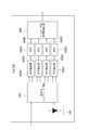
- FIGS. 1 is a block diagram showing a configuration of an optical receiver according to Embodiment 1 of the present invention.
- symbol shows the same or equivalent part.
- an optical receiver includes a local oscillation light source 100, a polarization diversity optical 90-degree hybrid circuit 200, four balanced photon detectors 300A, 300B, 300C, and 300D, and four analog-to-digital conversions.
- a device (ADC) 400A, 400B, 400C, 400D and a digital signal processing integrated circuit 500 are provided.
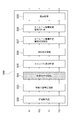
- FIG. 2 is a block diagram showing the configuration of the digital signal processing integrated circuit of the optical receiver according to Embodiment 1 of the present invention.
- a digital signal processing integrated circuit 500 includes a preprocessing circuit 502, a chromatic dispersion compensation circuit 503, a nonlinear equalization circuit 504, a timing extraction circuit 505, an adaptive equalization circuit 506, and a carrier frequency offset compensation circuit. 507, a carrier phase offset compensation circuit 508, and an identification circuit 509 are provided.
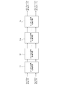
- FIG. 3 is a block diagram showing the configuration of the nonlinear equalization circuit according to Embodiment 1 of the present invention.
- a non-linear equalization circuit 504 is composed of N stages (N ⁇ 1) of digital signal processing circuits, and includes a first stage digital signal processing circuit 11, a second stage digital signal processing circuit 12, and m.
- An (m ⁇ N) -th stage digital signal processing circuit 1m and an N-th stage digital signal processing circuit 1N are provided.
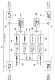
- FIG. 4 is a block diagram showing the configuration of the digital signal processing circuit according to the first embodiment of the present invention.
- FIG. 4 shows one stage (m-th stage) of N stages of digital signal processing circuits constituting the nonlinear equalization circuit 504.
- the digital signal processing circuit 1m includes two chromatic dispersion addition units 1A and 1B, two power calculation units 2A and 2B, four weighted averaging units 3A, 3B, 3C, and 3D, and four efficiency multiplications. 4A, 4B, 4C, 4D, two adders 5A, 5B, two complex phase rotation signal generation units 6A, 6B, two complex phase rotation units 7A, 7B, and two chromatic dispersion removal units 8A and 8B are provided.
- the chromatic dispersion adding units 1A and 1B and the chromatic dispersion removing units 8A and 8B can be realized by a finite-length impulse response filter in the time domain or the frequency domain.
- the m-th stage chromatic dispersion removal unit 8A (referred to as chromatic dispersion addition amount px) and the m + 1-th stage chromatic dispersion addition unit 1A (referred to as chromatic dispersion addition amount qx) are 2 Instead of being divided into two functional blocks, a single chromatic dispersion addition unit having a chromatic dispersion addition amount px + qx may be used.
- the m-th stage chromatic dispersion removal unit 8B (referred to as chromatic dispersion addition amount py) and the m + 1-th stage chromatic dispersion addition unit 1B (referred to as chromatic dispersion addition amount qy) are intentionally divided into two functional blocks.
- a single chromatic dispersion addition unit having a chromatic dispersion addition amount py + qy may be used. That is, among the N-stage (N ⁇ 2) digital signal processing circuits, the m (m ⁇ N) -th stage digital signal processing circuit has the transfer functions Hpost, z [m] (f) and Hpre, z [m + 1].
- the two linear filters (z ⁇ ⁇ x, y ⁇ ) represented by (f) may be realized as a single linear filter Hjoint, z [m: m + 1] (f).
- a local oscillation light source 100 of an optical receiver oscillates at a center wavelength approximately coincident with the center wavelength of an optical signal (received optical signal) input from an optical transmission line (not shown), and has a single wavelength CW (Continuous Wave) optical signal is generated, and this CW optical signal is output to the polarization diversity optical 90-degree hybrid circuit 200.
- CW Continuous Wave
- the optical 90-degree hybrid circuit 200 mixes a received optical signal input from an optical transmission line (not shown) and a CW optical signal input from the local oscillation light source 100, and outputs an optical signal in which eight kinds of interference are generated. To do.
- the optical 90-degree hybrid circuit 200 includes two orthogonal polarization modes (X / Y) of the received optical signal and a phase difference (0 degree / 180 degree / 90 degree) between the received optical signal and the CW optical signal. / 270 degrees), an X polarization (0 degree) interference light signal and an X polarization (180 degrees) interference light signal are output to the balanced photon detector 300A.
- the optical 90-degree hybrid circuit 200 outputs an X-polarized (90 degrees) interference optical signal and an X-polarized (270 degrees) interference optical signal to the balanced photon detector 300B, and outputs a Y-polarized light.
- the wave (0 degree) interference light signal and the Y polarization (180 degree) interference light signal are output to the balanced photon detector 300C, and the Y polarization (90 degree) interference light signal and the Y polarization
- the interference light signal of the wave (270 degrees) is output to the balanced photon detector 300D.
- the photon detector 300A square-detects the X-polarized (0 degree) interference optical signal and the X-polarized (180 degree) interference optical signal input from the optical 90-degree hybrid circuit 200, respectively, and converts them into electrical signals. Then, the difference between each electric signal is output to the analog-to-digital converter 400A.
- the photon detector 300B square-detects the X-polarized (90 degrees) interference optical signal and the X-polarized (270 degrees) interference optical signal input from the optical 90-degree hybrid circuit 200, respectively. It converts into a signal and outputs the difference of each electric signal to the analog-digital converter 400B.
- the photon detector 300C square-detects the Y-polarization (0 degree) interference optical signal and the Y-polarization (180 degree) interference optical signal input from the optical 90-degree hybrid circuit 200, respectively, and performs an electrical signal detection. And the difference between the electric signals is output to the analog-to-digital converter 400C.
- the photon detector 300D square-detects the Y-polarization (90 degrees) interference optical signal and the Y-polarization (270 degrees) interference optical signal input from the optical 90-degree hybrid circuit 200, respectively, and performs electrical detection. And the difference between the electric signals is output to the analog-to-digital converter 400D.
- the analog-to-digital converter 400A samples the electrical signal input from the photon detector 300A, and outputs the digital signal XI that has been discrete time and quantized to the digital signal processing integrated circuit 500.
- the analog-to-digital converter 400B samples the electrical signal input from the photon detector 300B, and outputs a digital signal XQ that has been discrete-timed and quantized to the digital signal processing integrated circuit 500.
- the analog-to-digital converter 400C samples the electrical signal input from the photon detector 300C, and outputs the digital signal YI that has been discrete time and quantized to the digital signal processing integrated circuit 500.
- the analog-to-digital converter 400D samples the electrical signal input from the photon detector 300D, and outputs the digital signal YQ that has been discrete time and quantized to the digital signal processing integrated circuit 500.
- the pre-processing circuit 502 of the digital signal processing integrated circuit 500 includes a digital signal XI input from the analog-digital converter 400A, a digital signal XQ input from the analog-digital converter 400B, and an input from the analog-digital converter 400C.
- Pre-processing such as amplitude normalization for suppressing amplitude variations of the four digital signals and deskew for delay difference correction with respect to the digital signal YI and the digital signal YQ input from the analog-digital converter 400D And outputs the four processed digital signals to the chromatic dispersion compensation circuit 503.
- the chromatic dispersion compensation circuit 503 roughly performs chromatic dispersion generated in the transmission path by performing linear waveform equalization by time domain equalization or frequency domain equalization on the four digital signals input from the preprocessing circuit 502. Four digital signals after 100% compensation and chromatic dispersion compensation are output to the nonlinear equalization circuit 504.
- the non-linear equalization circuit 504 applies non-linear equalization digital signal processing, which will be described later, to the four digital signals (considered as two pairs of complex signals) input from the chromatic dispersion compensation circuit 503, so that the non-linear equalization 4 Two digital signals (considered as two pairs of complex signals) are output to the timing extraction circuit 505.
- the timing extraction circuit 505 adaptively extracts the identification timing for the four digital signals input from the nonlinear equalization circuit 504, and performs feedback control on the sampling timing of the analog-digital converters 400A to 400D, thereby overrunning.
- Four digital data having a sampling rate of twice the sampling ratio are output to the adaptive equalization circuit 506.
- the adaptive equalization circuit 506 adaptively performs polarization multiplexing / demultiplexing on the four digital signals input from the timing extraction circuit 505 using an algorithm such as an envelope stabilization standard, and further, a transmission line
- the four digital signals compensated for PMD (polarization mode dispersion) and the like are output to the carrier frequency offset compensation circuit 507.
- the carrier frequency offset compensation circuit 507 compensates for the center frequency difference between the CW optical signal output from the local oscillation light source 100 and the received optical signal in the four digital signals input from the adaptive equalization circuit 506, and after compensation.
- the four digital signals are output to the carrier phase offset compensation circuit 508.
- the carrier phase offset compensation circuit 508 is a complex that uses the four digital signals input from the carrier frequency offset compensation circuit 507 as signal points for the X polarization component and the Y polarization component. In the plane, phase offset compensation is adaptively performed so that the signal points roughly converge to four points of 45 degrees, 135 degrees, -45 degrees, and -135 degrees, and the digital signal after the phase offset compensation is output to the identification circuit 509. To do.
- the identification circuit 509 performs binary identification on the four digital signals input from the carrier phase offset compensation circuit 508, and outputs the four binary signals after identification to the outside (not shown).
- the chromatic dispersion amount of the chromatic dispersion adding units 1A and 1B is set to ⁇ 600 ps / nm. That is, the first linear distortion adding unit (wavelength dispersion adding unit 1A) performs linear waveform distortion of the transfer function Hpre, x [m] (f) on the input complex digital signal sequence dx [m, i]. Append. Similarly, the second linear distortion adding unit (wavelength dispersion adding unit 1B) performs linear waveform distortion of the transfer function Hpre, y [m] (f) with respect to the input complex digital signal sequence dy [m, i]. Is added.
- the power calculation unit 2A calculates the square of the absolute value of the complex digital signal sequence after wavelength dispersion addition input from the wavelength dispersion addition unit 1A, that is, the power Px [m, i], and the weighted average unit 3A and the weighted average Output to part 3C.
- the power calculation unit 2B calculates the square of the absolute value of the complex digital signal sequence after wavelength dispersion addition input from the wavelength dispersion addition unit 1B, that is, the power Py [m, i], and the weighted average unit 3B. To the weighted average unit 3D.
- [M, i] Pavg, xy [m, i] is generated.
- [M, i] Pavg, yx [m, i] is generated.
- the adding unit 5A adds the nonlinear phase rotation amount ⁇ xx [m, i] input from the weighted average unit 4A and the nonlinear phase rotation amount ⁇ xy [m, i] input from the weighted average unit 4B.
- the result ⁇ x [m, i] ⁇ xx [m, i] + ⁇ xy [m, i] is output to the complex phase rotation signal generation unit 6A.
- the adding unit 5B adds the nonlinear phase rotation amount ⁇ yx [m, i] input from the weighted average unit 4C and the nonlinear phase rotation amount ⁇ yy [m, i] input from the weighted average unit 4D.
- the addition result ⁇ y [m, i] ⁇ yx [m, i] + ⁇ yy [m, i] is output to the complex phase rotation signal generation unit 6B.
- the complex phase rotation signal generation unit 6A converts ⁇ x [m, i] input from the addition unit 5A into a complex signal exp ( ⁇ j ⁇ x [m, i]) and outputs the complex signal to the complex phase rotation unit 7A.
- the complex phase rotation signal generation unit 6B converts ⁇ y [m, i] input from the addition unit 5B into a complex signal exp ( ⁇ j ⁇ y [m, i]) and outputs it to the complex phase rotation unit 7. To do.
- the complex phase rotator 7A includes a complex digital signal sequence to which chromatic dispersion is input from the chromatic dispersion adder 1A and a complex signal exp ( ⁇ j ⁇ x [m, i) input from the complex phase rotation signal generator 6A. ]), The inverse operation of the nonlinear phase rotation of the transmission line is performed, and the calculated signal is output to the chromatic dispersion removing unit 8A.
- the complex phase rotation unit 7B includes a complex digital signal sequence to which chromatic dispersion is input, which is input from the chromatic dispersion addition unit 1B, and a complex signal exp ( ⁇ j ⁇ y [ m, i]) is multiplied by the inverse operation of the non-linear phase rotation of the transmission line, and the calculated complex digital signal is output to the chromatic dispersion removing unit 8B.
- the chromatic dispersion removing unit 8A gives the chromatic dispersion of opposite polarity to the complex digital signal input from the complex phase rotating unit 7A so as to remove the chromatic dispersion added by the chromatic dispersion adding unit 1A, and the complex signal after adding the chromatic dispersion is added.
- the digital signal d′ x “m” E′xi [m] + jE′xq [m] is output to the next stage.
- the chromatic dispersion removal unit 8B gives chromatic dispersion of opposite polarity to the complex digital signal input from the complex phase rotation unit 7B so as to remove the chromatic dispersion added by the chromatic dispersion addition unit 1B, and adds chromatic dispersion.
- the subsequent complex digital signal d′ y “m” E′yi [m] + jE′yq [m] is output to the next stage.
- the first linear distortion removing unit (wavelength dispersion removing unit 8A) has a linear waveform distortion transfer function Hpre, x [m] with respect to the complex digital signal given the complex phase rotation by the complex phase rotating unit 7A.
- Waveform distortion having the inverse function Hpre, x [m] ⁇ 1 (f) of (f) or the complex conjugate function Hpre, x [m] * (f) as the transfer function Hpost, x [m] (f) is added.
- the waveform distortion in the first linear distortion adding unit is removed.
- the second linear distortion removal unit (wavelength dispersion removal unit 8B) has a linear waveform distortion transfer function Hpre, y [m] with respect to the complex digital signal given the complex phase rotation by the complex phase rotation unit 7B. ]
- Add waveform distortion having inverse function Hpre, y [m] ⁇ 1 (f) or complex conjugate function Hpre, y [m] * (f) as transfer function Hpost, y [m] (f) By doing so, the waveform distortion in the second linear distortion adding section is removed.
- the chromatic dispersion adding unit 1A and the chromatic dispersion adding unit 1B add chromatic dispersion of ⁇ 600 ps / nm
- the chromatic dispersion removing unit 8A and the chromatic dispersion removing unit 8B add chromatic dispersion of +600 ps / nm.
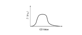
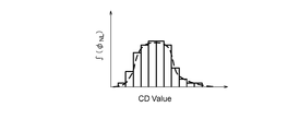
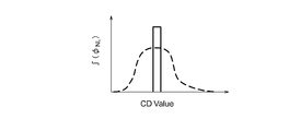
- FIG. 5A, 5B, and 5C are diagrams showing the relationship between the chromatic dispersion value of the digital signal processing circuit according to the first embodiment of the present invention and the accumulated nonlinear phase rotation amount, and simplification thereof.
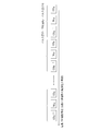
- FIG. 6 is a diagram showing the concept of nonlinear equalization of the nonlinear equalizer circuit according to Embodiment 1 of the present invention.
- the integrated value ( ⁇ NL [i] of the nonlinear phase rotation amount given under a specific intersymbol interference condition (for example, the specific chromatic dispersion value CD [i]). ]) Respectively.
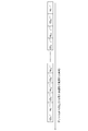
- the relationship between the chromatic dispersion value (horizontal axis: CD Value) and the integrated nonlinear phase rotation amount (vertical axis: ⁇ NL) is obtained.
- discretization is possible as shown in FIG. 5B, and most simply, it can be represented by a single chromatic dispersion value as shown in FIG. 5C.
- the degree of discretization of the chromatic dispersion value increases, the equalization ability decreases.
- Non-linear equalization is realized by providing a single stage and providing a plurality of stages of similar digital signal processing circuits.
- the function of the digital signal processing integrated circuit 500 of the optical receiver is simulated by a computer, and the dependence of the nonlinear equalization circuit 504 on the number of equalization stages will be described with reference to FIGS.
- FIG. 7 is a block diagram showing a configuration simulating the function of the digital signal processing integrated circuit of the optical receiver according to the first embodiment of the present invention.
- FIG. 8 is a diagram showing the equalization stage number dependency of the nonlinear equalization circuit according to the first embodiment of the present invention.
- FIG. 7 shows a functional block configuration of the entire digital signal processing integrated circuit 500 used for offline analysis.
- Rate conversion unit 501 preprocessing unit 502A, chromatic dispersion compensation unit 503A, nonlinear equalization unit 504A, timing extraction unit 505A, adaptive equalization unit 506A, carrier frequency offset compensation unit 507A, carrier phase offset A compensation unit 508A, an identification unit 509A, and a Q value calculation unit 510 are provided.
- Rate conversion unit 501 preprocessing unit 502A
- chromatic dispersion compensation unit 503A nonlinear equalization unit 504A
- timing extraction unit 505A adaptive equalization unit 506A
- carrier frequency offset compensation unit 507A carrier phase offset A compensation unit 508A
- an identification unit 509A an identification unit 509A
- Q value calculation unit 510 Q value calculation unit
- the rate converter 501 converts the sampling rate of four digital signals input from outside (not shown) (data acquired by a digital sampling oscilloscope) to a speed synchronized with the bit rate of 43 Gb / s, and converts the four digital signals after the rate conversion.
- the digital signal was output to the preprocessing unit 502A.
- the pre-processing unit 502A performs pre-processing such as amplitude normalization for suppressing amplitude variations of the four digital signals and deskew for delay difference correction, and the four digital signals after processing are processed into the chromatic dispersion compensation unit 503A. Output to.
- the chromatic dispersion compensation unit 503A compensates chromatic dispersion generated in the transmission path for the four digital signals input from the preprocessing unit 502A, and outputs the four digital signals after chromatic dispersion compensation to the nonlinear equalization unit 504A. did.
- the nonlinear equalization unit 504A performs nonlinear equalization digital signal processing corresponding to the processing of the nonlinear equalization circuit 504 on the four digital signals (considered as two pairs of complex signals) input from the chromatic dispersion compensation unit 503A.
- the four digital signals after application of nonlinear equalization were output to the timing extraction unit 505A.
- the timing extraction unit 505A adaptively extracts identification timings from the four digital signals input from the nonlinear equalization unit 504A and adaptively equalizes four digital data having a sampling rate of twice the oversampling ratio. Output to 506A.
- the adaptive equalization unit 506A adaptively performs polarization multiplexing / demultiplexing on the four digital signals input from the timing extraction unit 505A by using an algorithm such as an envelope constant standard, and further, a transmission line
- the four digital signals compensated for PMD and the like are output to the carrier frequency offset compensation unit 507A.
- the carrier frequency offset compensation unit 507A compensates for the center frequency difference between the continuous optical signal output from the local oscillation light source 100 and the received optical signal in the four digital signals input from the adaptive equalization unit 506A. Four digital signals were output to the carrier phase offset compensation unit 508A.
- the carrier phase offset compensator 508A has a complex signal centered on the I axis and the Q axis for the X polarization component and the Y polarization component for the four digital signals input from the carrier frequency offset compensation unit 507A. In the plane, adaptively perform phase offset compensation so that the signal points are roughly converged to four points of 45 degrees, 135 degrees, -45 degrees, and -135 degrees, and output the digital signal after the phase offset compensation to the identification unit 509A. did.
- the identification unit 509A performs binary identification on the four digital signals input from the carrier phase offset compensation unit 508A, and outputs the four binary signals after identification to the Q value calculation unit 510.
- the Q value calculation unit 510 calculates the code error rate of the four binary signals input from the identification unit 509A, and calculates the Q value that is an index of transmission performance in optical communication.
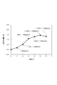
- FIG. 8 shows the result of plotting an example of the improvement amount of the Q value, which is an index indicating the transmission performance of optical communication, with respect to the number of equalization stages, that is, the number of stages N of the digital signal processing circuit.
- the modulation method is polarization multiplexed QPSK
- the bit rate is 43 Gb / s
- 5000 km transmission is performed by the cyclic transmission test
- the continuous optical signal and the received optical signal output from the local oscillation light source 100 in the optical receiver are After mixing, detection was performed by four balanced photon detectors 300A-D.
- each signal of the X polarization I axis, the X polarization Q axis, the Y polarization I axis, and the Y polarization Q axis is analog-to-digital converted by the four analog-digital converters 400A-D, and the digital sampling oscilloscope is used.
- 4 serial data were accumulated at a sampling rate of 40 Gsample / s.
- the equalization ability was confirmed by off-line analysis on a computer.
- the chromatic dispersion amounts of the first, second, third, and fourth stages were ⁇ 900 ps / nm, ⁇ 700 ps / nm, ⁇ 500 ps / nm, and ⁇ 300 ps / nm.
- N 4
- the chromatic dispersion amounts of the first, second, third, fourth, and fifth stages are ⁇ 1000 ps / nm, ⁇ 800 ps / nm, ⁇ 600 ps / nm, ⁇ 400 ps / nm, ⁇ 200 ps / nm.
- the first stage, the second stage, the third stage, the fourth stage, the fifth stage, and the sixth stage have chromatic dispersion amounts of ⁇ 1100 ps / nm, ⁇ 900 ps / nm, ⁇ 700 ps / nm, ⁇ 500 ps / nm, ⁇ 300 ps / nm, and ⁇ 100 ps / nm.
- These setting methods are not optimal and are examples.
Landscapes
- Engineering & Computer Science (AREA)
- Computer Networks & Wireless Communication (AREA)
- Signal Processing (AREA)
- Physics & Mathematics (AREA)
- Nonlinear Science (AREA)
- Electromagnetism (AREA)
- Optical Communication System (AREA)
Abstract
La présente invention concerne un récepteur optique pourvu d'au moins un circuit intégré de traitement de signal numérique. Ledit circuit intégré de traitement de signal numérique comprend au moins un circuit d'égalisation non linéaire qui applique un traitement de signal numérique par égalisation non linéaire à quatre signaux numériques. Le circuit d'égalisation non linéaire est formé de N rangées (N ≥ 1) de circuits de traitement de signal numérique, et, parmi les N rangées de circuits de traitement de signal numérique, la mième rangée comporte une première unité d'ajout de distorsion linéaire qui ajoute une distorsion linéaire à une séquence complexe de signaux numériques (dx[m, i]) entrée, et une première unité de suppression de distorsion linéaire qui supprime une distorsion de forme d'onde présente dans la première unité d'ajout de distorsion linéaire en ajoutant une distorsion de forme d'onde au signal numérique complexe auquel une rotation de phase complexe a été appliquée.
Priority Applications (2)
| Application Number | Priority Date | Filing Date | Title |
|---|---|---|---|
| PCT/JP2011/053499 WO2012111140A1 (fr) | 2011-02-18 | 2011-02-18 | Récepteur optique, circuit d'égalisation non linéaire et circuit de traitement de signal numérique |
| JP2012557753A JP5523591B2 (ja) | 2011-02-18 | 2011-02-18 | 光受信器、非線形等化回路及びデジタル信号処理回路 |
Applications Claiming Priority (1)
| Application Number | Priority Date | Filing Date | Title |
|---|---|---|---|
| PCT/JP2011/053499 WO2012111140A1 (fr) | 2011-02-18 | 2011-02-18 | Récepteur optique, circuit d'égalisation non linéaire et circuit de traitement de signal numérique |
Publications (1)
| Publication Number | Publication Date |
|---|---|
| WO2012111140A1 true WO2012111140A1 (fr) | 2012-08-23 |
Family
ID=46672101
Family Applications (1)
| Application Number | Title | Priority Date | Filing Date |
|---|---|---|---|
| PCT/JP2011/053499 Ceased WO2012111140A1 (fr) | 2011-02-18 | 2011-02-18 | Récepteur optique, circuit d'égalisation non linéaire et circuit de traitement de signal numérique |
Country Status (2)
| Country | Link |
|---|---|
| JP (1) | JP5523591B2 (fr) |
| WO (1) | WO2012111140A1 (fr) |
Cited By (8)
| Publication number | Priority date | Publication date | Assignee | Title |
|---|---|---|---|---|
| JP2012186807A (ja) * | 2011-03-04 | 2012-09-27 | Fujitsu Ltd | 非線形劣化補償方法および装置 |
| WO2013042345A1 (fr) * | 2011-09-22 | 2013-03-28 | 日本電気株式会社 | Dispositif de traitement de signal optique, dispositif de traitement de polarisation et procédé de traitement de signal optique |
| WO2014122815A1 (fr) * | 2013-02-07 | 2014-08-14 | 日本電気株式会社 | Dispositif de traitement de signaux et procédé de traitement de signaux |
| WO2014167897A1 (fr) * | 2013-04-09 | 2014-10-16 | 日本電気株式会社 | Dispositif de traitement de signal et procédé de traitement de signal |
| WO2015131841A3 (fr) * | 2014-03-07 | 2016-01-07 | Huawei Technologies Co., Ltd. | Système et procédé de détection optique directe à tolérance de dispersion chromatique |
| JP2016025513A (ja) * | 2014-07-22 | 2016-02-08 | 日本電信電話株式会社 | コヒーレント光受信機 |
| JPWO2021210259A1 (fr) * | 2020-04-14 | 2021-10-21 | ||
| JP2024106335A (ja) * | 2023-01-26 | 2024-08-07 | ノキア ソリューションズ アンド ネットワークス オサケユキチュア | 摂動ベース硬判定非線形性補償 |
Families Citing this family (1)
| Publication number | Priority date | Publication date | Assignee | Title |
|---|---|---|---|---|
| JP3384800B2 (ja) | 1990-10-12 | 2003-03-10 | ナトコ株式会社 | 被覆組成物 |
Citations (3)
| Publication number | Priority date | Publication date | Assignee | Title |
|---|---|---|---|---|
| JP2010050578A (ja) * | 2008-08-19 | 2010-03-04 | Fujitsu Ltd | 歪補償器、光受信装置およびそれらの制御方法並びに光伝送システム |
| JP2010268210A (ja) * | 2009-05-14 | 2010-11-25 | Nippon Telegr & Teleph Corp <Ntt> | 光受信装置及び光受信方法 |
| JP2011015013A (ja) * | 2009-06-30 | 2011-01-20 | Fujitsu Ltd | 信号処理装置、光受信装置、検出装置および波形歪補償方法 |
-
2011
- 2011-02-18 WO PCT/JP2011/053499 patent/WO2012111140A1/fr not_active Ceased
- 2011-02-18 JP JP2012557753A patent/JP5523591B2/ja not_active Expired - Fee Related
Patent Citations (3)
| Publication number | Priority date | Publication date | Assignee | Title |
|---|---|---|---|---|
| JP2010050578A (ja) * | 2008-08-19 | 2010-03-04 | Fujitsu Ltd | 歪補償器、光受信装置およびそれらの制御方法並びに光伝送システム |
| JP2010268210A (ja) * | 2009-05-14 | 2010-11-25 | Nippon Telegr & Teleph Corp <Ntt> | 光受信装置及び光受信方法 |
| JP2011015013A (ja) * | 2009-06-30 | 2011-01-20 | Fujitsu Ltd | 信号処理装置、光受信装置、検出装置および波形歪補償方法 |
Non-Patent Citations (1)
| Title |
|---|
| KAZURO KIKUCHI: "Electronic post-compensation for Nonlinear Phase Fluctuations in a 1000-km 20-Gbit/s Optical Quadrature Phase-shift Keying Transmission System Using the Digital Coherent Receiver", OPTICS EXPRESS, vol. 16, no. 2, 21 January 2008 (2008-01-21), pages 889 - 896, XP002557255, DOI: doi:10.1364/OE.16.000889 * |
Cited By (15)
| Publication number | Priority date | Publication date | Assignee | Title |
|---|---|---|---|---|
| JP2012186807A (ja) * | 2011-03-04 | 2012-09-27 | Fujitsu Ltd | 非線形劣化補償方法および装置 |
| WO2013042345A1 (fr) * | 2011-09-22 | 2013-03-28 | 日本電気株式会社 | Dispositif de traitement de signal optique, dispositif de traitement de polarisation et procédé de traitement de signal optique |
| JPWO2014122815A1 (ja) * | 2013-02-07 | 2017-01-26 | 日本電気株式会社 | 信号処理装置及び信号処理方法 |
| WO2014122815A1 (fr) * | 2013-02-07 | 2014-08-14 | 日本電気株式会社 | Dispositif de traitement de signaux et procédé de traitement de signaux |
| US9831956B2 (en) | 2013-02-07 | 2017-11-28 | Nec Corporation | Signal processing device and signal processing method |
| WO2014167897A1 (fr) * | 2013-04-09 | 2014-10-16 | 日本電気株式会社 | Dispositif de traitement de signal et procédé de traitement de signal |
| JPWO2014167897A1 (ja) * | 2013-04-09 | 2017-02-16 | 日本電気株式会社 | 信号処理装置及び信号処理方法 |
| US9853765B2 (en) | 2013-04-09 | 2017-12-26 | Nec Corporation | Signal processing device and signal processing method for optical polarization multiplexed signal |
| WO2015131841A3 (fr) * | 2014-03-07 | 2016-01-07 | Huawei Technologies Co., Ltd. | Système et procédé de détection optique directe à tolérance de dispersion chromatique |
| JP2016025513A (ja) * | 2014-07-22 | 2016-02-08 | 日本電信電話株式会社 | コヒーレント光受信機 |
| JPWO2021210259A1 (fr) * | 2020-04-14 | 2021-10-21 | ||
| WO2021210259A1 (fr) * | 2020-04-14 | 2021-10-21 | 日本電気株式会社 | Dispositif de mise à jour de coefficient de filtre, dispositif de filtre, dispositif de démodulation, dispositif de réception, système d'émission et de réception, procédé de mise à jour de coefficient de filtre et support d'enregistrement |
| JP7501613B2 (ja) | 2020-04-14 | 2024-06-18 | 日本電気株式会社 | フィルタ係数更新装置、フィルタ装置、復調装置及びフィルタ係数更新方法 |
| JP2024106335A (ja) * | 2023-01-26 | 2024-08-07 | ノキア ソリューションズ アンド ネットワークス オサケユキチュア | 摂動ベース硬判定非線形性補償 |
| JP7771236B2 (ja) | 2023-01-26 | 2025-11-17 | ノキア ソリューションズ アンド ネットワークス オサケユキチュア | 摂動ベース硬判定非線形性補償 |
Also Published As
| Publication number | Publication date |
|---|---|
| JPWO2012111140A1 (ja) | 2014-07-03 |
| JP5523591B2 (ja) | 2014-06-18 |
Similar Documents
| Publication | Publication Date | Title |
|---|---|---|
| JP5523591B2 (ja) | 光受信器、非線形等化回路及びデジタル信号処理回路 | |
| US8909066B2 (en) | Optical transfer system, optical transmission device, and optical reception device | |
| US20150372764A1 (en) | Optical receiver having an equalization filter with an integrated signal re-sampler | |
| Füllner et al. | Transmission of 80-GBd 16-QAM over 300 km and Kramers-Kronig reception using a low-complexity FIR Hilbert filter approximation | |
| US9369213B1 (en) | Demultiplexing processing for a receiver | |
| WO2016103631A1 (fr) | Dispositif de traitement de signal numérique, récepteur optique numérique l'utilisant et procédé de traitement de signal numérique | |
| JP2015056753A (ja) | 非線形歪み補償装置及び方法並びに光受信器 | |
| US9692521B1 (en) | Polarization pre-compensation technique for polarization-division-multiplexed direct-detection optical communication systems | |
| US20150256267A1 (en) | Optical receiver having a digital chromatic-dispersion compensator based on real-valued arithmetic | |
| US20120301157A1 (en) | Chromatic dispersion compensation using sign operations and lookup tables | |
| Xu et al. | Joint scheme of dynamic polarization demultiplexing and PMD compensation up to second order for flexible receivers | |
| JP2009218837A (ja) | 光受信装置および光受信方法 | |
| Rosenkranz et al. | Electrical equalization for advanced optical communication systems | |
| Nambath et al. | First demonstration of an all analog adaptive equalizer for coherent DP-QPSK links | |
| WO2023073927A1 (fr) | Circuit de traitement de signal numérique, procédé, récepteur et système de communication | |
| Kottke et al. | Coherent UDWDM PON with joint subcarrier reception at OLT | |
| Yang et al. | Modulation format independent blind polarization demultiplexing algorithms for elastic optical networks | |
| Savory | Electronic signal processing in optical communications | |
| WO2013140970A1 (fr) | Système de communication optique et procédé de communication optique ayant une haute résistance de bruit de phase | |
| Hoshida et al. | Digital nonlinear compensation techniques for high-speed DWDM transmission systems | |
| WO2023067641A1 (fr) | Circuit de traitement de signal numérique, procédé, récepteur et système de communication | |
| Liu et al. | Electronic dispersion compensation based on optical field reconstruction with orthogonal differential direct-detection and digital signal processing | |
| Czegledi et al. | Modulation format independent joint polarization and phase tracking for coherent receivers | |
| Faruk et al. | Frequency-domain adaptive equalizer with rational oversampling rates in coherent optical receivers | |
| JPWO2015052894A1 (ja) | 搬送波周波数偏差推定装置および搬送波周波数偏差推定方法 |
Legal Events
| Date | Code | Title | Description |
|---|---|---|---|
| 121 | Ep: the epo has been informed by wipo that ep was designated in this application |
Ref document number: 11858733 Country of ref document: EP Kind code of ref document: A1 |
|
| WWE | Wipo information: entry into national phase |
Ref document number: 2012557753 Country of ref document: JP |
|
| NENP | Non-entry into the national phase |
Ref country code: DE |
|
| 122 | Ep: pct application non-entry in european phase |
Ref document number: 11858733 Country of ref document: EP Kind code of ref document: A1 |