WO2012111140A1 - 光受信器、非線形等化回路及びデジタル信号処理回路 - Google Patents
光受信器、非線形等化回路及びデジタル信号処理回路 Download PDFInfo
- Publication number
- WO2012111140A1 WO2012111140A1 PCT/JP2011/053499 JP2011053499W WO2012111140A1 WO 2012111140 A1 WO2012111140 A1 WO 2012111140A1 JP 2011053499 W JP2011053499 W JP 2011053499W WO 2012111140 A1 WO2012111140 A1 WO 2012111140A1
- Authority
- WO
- WIPO (PCT)
- Prior art keywords
- complex
- phase rotation
- digital signal
- unit
- weighted average
- Prior art date
- Legal status (The legal status is an assumption and is not a legal conclusion. Google has not performed a legal analysis and makes no representation as to the accuracy of the status listed.)
- Ceased
Links
Images


Classifications
-
- H—ELECTRICITY
- H04—ELECTRIC COMMUNICATION TECHNIQUE
- H04B—TRANSMISSION
- H04B10/00—Transmission systems employing electromagnetic waves other than radio-waves, e.g. infrared, visible or ultraviolet light, or employing corpuscular radiation, e.g. quantum communication
- H04B10/60—Receivers
- H04B10/61—Coherent receivers
- H04B10/616—Details of the electronic signal processing in coherent optical receivers
- H04B10/6163—Compensation of non-linear effects in the fiber optic link, e.g. self-phase modulation [SPM], cross-phase modulation [XPM], four wave mixing [FWM]
-
- H—ELECTRICITY
- H04—ELECTRIC COMMUNICATION TECHNIQUE
- H04L—TRANSMISSION OF DIGITAL INFORMATION, e.g. TELEGRAPHIC COMMUNICATION
- H04L27/00—Modulated-carrier systems
- H04L27/0014—Carrier regulation
-
- H—ELECTRICITY
- H04—ELECTRIC COMMUNICATION TECHNIQUE
- H04L—TRANSMISSION OF DIGITAL INFORMATION, e.g. TELEGRAPHIC COMMUNICATION
- H04L27/00—Modulated-carrier systems
- H04L27/01—Equalisers
-
- H—ELECTRICITY
- H04—ELECTRIC COMMUNICATION TECHNIQUE
- H04L—TRANSMISSION OF DIGITAL INFORMATION, e.g. TELEGRAPHIC COMMUNICATION
- H04L27/00—Modulated-carrier systems
- H04L27/18—Phase-modulated carrier systems, i.e. using phase-shift keying
- H04L27/22—Demodulator circuits; Receiver circuits
- H04L27/223—Demodulation in the optical domain
-
- H—ELECTRICITY
- H04—ELECTRIC COMMUNICATION TECHNIQUE
- H04L—TRANSMISSION OF DIGITAL INFORMATION, e.g. TELEGRAPHIC COMMUNICATION
- H04L27/00—Modulated-carrier systems
- H04L27/0014—Carrier regulation
- H04L2027/0024—Carrier regulation at the receiver end
- H04L2027/0026—Correction of carrier offset
- H04L2027/0038—Correction of carrier offset using an equaliser
-
- H—ELECTRICITY
- H04—ELECTRIC COMMUNICATION TECHNIQUE
- H04L—TRANSMISSION OF DIGITAL INFORMATION, e.g. TELEGRAPHIC COMMUNICATION
- H04L27/00—Modulated-carrier systems
- H04L27/0004—Modulated-carrier systems using wavelets
-
- H—ELECTRICITY
- H04—ELECTRIC COMMUNICATION TECHNIQUE
- H04L—TRANSMISSION OF DIGITAL INFORMATION, e.g. TELEGRAPHIC COMMUNICATION
- H04L5/00—Arrangements affording multiple use of the transmission path
- H04L5/02—Channels characterised by the type of signal
- H04L5/04—Channels characterised by the type of signal the signals being represented by different amplitudes or polarities, e.g. quadriplex
Definitions
- the present invention relates to an optical receiver of an optical transmission system using a digital coherent system and a non-linear equalization circuit including an N (N ⁇ 1) stage digital signal processing circuit.
- BPSK binary phase-shift keying
- QPSK quaternary PSK
- OOK on-off keying
- Quaternary Phase-Shift Keying
- QPSK and 16QAM are transmitted by assigning signals to the same phase axis (I axis: In-Phase axis) and quadrature phase axis (Q axis: Quadrature-Phase axis) in the optical transmitter on the transmission side of the optical transmission system. To do.
- a direct detection method such as a square detection method or a delay detection method has been used as an optical signal detection method.
- an optical signal can be detected without having a local oscillation light source in the optical receiver, and the optical receiver can be mounted simply and at low cost.
- a digital coherent system that receives digital signal processing in combination with a synchronous detection system having a local oscillation light source in an optical receiver has attracted attention (for example, see Non-Patent Document 1).
- linear photoelectric conversion by synchronous detection and fixed, semi-fixed, and adaptive linear equalization by digital signal processing enable stable polarization multiplexed signal separation and waveform in optical receivers. Distortion compensation is possible. For this reason, it is possible to realize excellent equalization characteristics and excellent noise tolerance against linear waveform distortion caused by chromatic dispersion or polarization mode dispersion (PMD) generated in the optical transmission line.
- PMD polarization mode dispersion
- FIG. 9 is a diagram illustrating a configuration example of a multi-relay optical transmission line and a concept of a sequential calculation method of forward propagation.
- the fiber nonlinear optical effect causes a significant deterioration in transmission quality.
- Propagation in the optical fiber is described by a nonlinear Schrodinger equation, and a split-step Fourier method (SSFM) is used as a sequential calculation method.
- SSFM split-step Fourier method
- an optical transmission line is divided into short sections (sections that are sufficiently shorter than one relay section of a multi-relay system), linear effects such as transmission loss and chromatic dispersion (CD), and nonlinear phase that is self-phase modulation. Sequential calculation that alternately incorporates non-linear effects such as rotation (NL) is performed (see FIG. 9).
- FIG. 10 is a diagram illustrating the concept of the digital back propagation method.
- this digital back-propagation method is a method of obtaining an optical waveform without distortion at the transmission end by performing propagation calculation in the direction opposite to the transmission direction by SSFM.
- signal processing is usually performed at most in several sections / relays to 10 sections / relays.
- Non-Patent Document 2 since the SSFM is solved in the direction opposite to the transmission direction, there is a problem that the circuit scale increases in proportion to the number of relays.
- the present invention has been made to solve the above-described problems, and is capable of equalizing waveform distortion caused by the fiber nonlinear optical effect with a circuit scale and power consumption smaller than those of the digital back propagation method.
- An object of the present invention is to obtain an optical receiver and a non-linear equalization circuit capable of improving the quality.
- An optical receiver includes a local oscillation light source that generates an optical signal that oscillates at the same center wavelength as a received optical signal, and a polarization that mixes the received optical signal and an optical signal output from the local oscillation light source.
- Wave diversity optical 90 degree hybrid circuit, four balanced photon detectors that detect four pairs of optical signals output from the optical 90 degree hybrid circuit, and 4 output from the four photon detectors Four analog-digital converters for analog-digital conversion of two electrical signals and a digital signal processing integrated circuit connected to the four analog-digital converters are provided.
- the digital signal processing integrated circuit of the optical receiver includes a chromatic dispersion compensation circuit that compensates for chromatic dispersion of an optical transmission line for four digital signals, and a non-linear function for the four digital signals.
- a non-linear equalization circuit that applies optimized digital signal processing, an adaptive equalization circuit that compensates for polarization mode dispersion of a transmission line and separates polarization multiplexed signals for four digital signals, and four digital signals
- a carrier frequency offset compensation circuit that compensates for a center frequency difference between the received optical signal and the optical signal output from the local oscillation light source, and the received optical signal and the local for four digital signals.
- at least a carrier phase offset compensation circuit that compensates for an optical phase difference with an optical signal output from the oscillation light source.
- the non-linear equalization circuit of the digital signal processing integrated circuit of the optical receiver according to the present invention is composed of N stages (N ⁇ 1) of digital signal processing circuits.
- the digital signal processing circuit at the stage adds the first linear distortion that adds the linear distortion of the transfer function Hpre, x [m] (f) to the input first complex digital signal sequence dx [m, i].
- a second linear distortion adding unit that adds a linear distortion of the transfer function Hpre, y [m] (f) to the input second complex digital signal sequence dy [m, i], and a linear distortion.
- phase rotation amount ⁇ xy [m, i] ⁇ xy [m, i] Pavg, xy [m, i]
- An adder a first complex phase rotation signal generation unit that
- a first complex phase rotation unit that gives a complex phase rotation by multiplying exp ( ⁇ j ⁇ x [m, i]); and the complex signal exp ( ⁇ j ⁇ y [m, i]) is multiplied by a second complex phase rotator that gives a complex phase rotation, and the complex digital signal is given the complex phase rotation by the first complex phase rotator.
- the transfer function Hpre, y [m] (f) of the inverse function Hpre, y [m] ⁇ 1 (f) or the complex conjugate function Hpre, y [m] * (f) is transferred to the transfer function Hpost, y [m] (f).
- a second linear distortion removing unit that removes the waveform distortion in the second linear distortion adding unit by adding the waveform distortion included in f).
- the optical receiver according to the present invention can equalize the waveform distortion caused by the fiber nonlinear optical effect with a smaller circuit scale and power consumption than the digital back propagation method, and can improve the transmission quality.
- FIG. 1 is a block diagram showing a configuration of a nonlinear equalizer circuit according to Embodiment 1 of the present invention.
- FIG. 1 is a block diagram showing a configuration of a digital signal processing circuit according to Embodiment 1 of the present invention. It is a figure which shows the relationship between the chromatic dispersion value of the digital signal processing circuit which concerns on Example 1 of this invention, and the integrated nonlinear phase rotation amount, and its simplification.
- Embodiment 1 of the present invention will be described below.
- FIGS. 1 is a block diagram showing a configuration of an optical receiver according to Embodiment 1 of the present invention.
- symbol shows the same or equivalent part.
- an optical receiver includes a local oscillation light source 100, a polarization diversity optical 90-degree hybrid circuit 200, four balanced photon detectors 300A, 300B, 300C, and 300D, and four analog-to-digital conversions.
- a device (ADC) 400A, 400B, 400C, 400D and a digital signal processing integrated circuit 500 are provided.
- FIG. 2 is a block diagram showing the configuration of the digital signal processing integrated circuit of the optical receiver according to Embodiment 1 of the present invention.
- a digital signal processing integrated circuit 500 includes a preprocessing circuit 502, a chromatic dispersion compensation circuit 503, a nonlinear equalization circuit 504, a timing extraction circuit 505, an adaptive equalization circuit 506, and a carrier frequency offset compensation circuit. 507, a carrier phase offset compensation circuit 508, and an identification circuit 509 are provided.
- FIG. 3 is a block diagram showing the configuration of the nonlinear equalization circuit according to Embodiment 1 of the present invention.
- a non-linear equalization circuit 504 is composed of N stages (N ⁇ 1) of digital signal processing circuits, and includes a first stage digital signal processing circuit 11, a second stage digital signal processing circuit 12, and m.
- An (m ⁇ N) -th stage digital signal processing circuit 1m and an N-th stage digital signal processing circuit 1N are provided.
- FIG. 4 is a block diagram showing the configuration of the digital signal processing circuit according to the first embodiment of the present invention.
- FIG. 4 shows one stage (m-th stage) of N stages of digital signal processing circuits constituting the nonlinear equalization circuit 504.
- the digital signal processing circuit 1m includes two chromatic dispersion addition units 1A and 1B, two power calculation units 2A and 2B, four weighted averaging units 3A, 3B, 3C, and 3D, and four efficiency multiplications. 4A, 4B, 4C, 4D, two adders 5A, 5B, two complex phase rotation signal generation units 6A, 6B, two complex phase rotation units 7A, 7B, and two chromatic dispersion removal units 8A and 8B are provided.
- the chromatic dispersion adding units 1A and 1B and the chromatic dispersion removing units 8A and 8B can be realized by a finite-length impulse response filter in the time domain or the frequency domain.
- the m-th stage chromatic dispersion removal unit 8A (referred to as chromatic dispersion addition amount px) and the m + 1-th stage chromatic dispersion addition unit 1A (referred to as chromatic dispersion addition amount qx) are 2 Instead of being divided into two functional blocks, a single chromatic dispersion addition unit having a chromatic dispersion addition amount px + qx may be used.
- the m-th stage chromatic dispersion removal unit 8B (referred to as chromatic dispersion addition amount py) and the m + 1-th stage chromatic dispersion addition unit 1B (referred to as chromatic dispersion addition amount qy) are intentionally divided into two functional blocks.
- a single chromatic dispersion addition unit having a chromatic dispersion addition amount py + qy may be used. That is, among the N-stage (N ⁇ 2) digital signal processing circuits, the m (m ⁇ N) -th stage digital signal processing circuit has the transfer functions Hpost, z [m] (f) and Hpre, z [m + 1].
- the two linear filters (z ⁇ ⁇ x, y ⁇ ) represented by (f) may be realized as a single linear filter Hjoint, z [m: m + 1] (f).
- a local oscillation light source 100 of an optical receiver oscillates at a center wavelength approximately coincident with the center wavelength of an optical signal (received optical signal) input from an optical transmission line (not shown), and has a single wavelength CW (Continuous Wave) optical signal is generated, and this CW optical signal is output to the polarization diversity optical 90-degree hybrid circuit 200.
- CW Continuous Wave
- the optical 90-degree hybrid circuit 200 mixes a received optical signal input from an optical transmission line (not shown) and a CW optical signal input from the local oscillation light source 100, and outputs an optical signal in which eight kinds of interference are generated. To do.
- the optical 90-degree hybrid circuit 200 includes two orthogonal polarization modes (X / Y) of the received optical signal and a phase difference (0 degree / 180 degree / 90 degree) between the received optical signal and the CW optical signal. / 270 degrees), an X polarization (0 degree) interference light signal and an X polarization (180 degrees) interference light signal are output to the balanced photon detector 300A.
- the optical 90-degree hybrid circuit 200 outputs an X-polarized (90 degrees) interference optical signal and an X-polarized (270 degrees) interference optical signal to the balanced photon detector 300B, and outputs a Y-polarized light.
- the wave (0 degree) interference light signal and the Y polarization (180 degree) interference light signal are output to the balanced photon detector 300C, and the Y polarization (90 degree) interference light signal and the Y polarization
- the interference light signal of the wave (270 degrees) is output to the balanced photon detector 300D.
- the photon detector 300A square-detects the X-polarized (0 degree) interference optical signal and the X-polarized (180 degree) interference optical signal input from the optical 90-degree hybrid circuit 200, respectively, and converts them into electrical signals. Then, the difference between each electric signal is output to the analog-to-digital converter 400A.
- the photon detector 300B square-detects the X-polarized (90 degrees) interference optical signal and the X-polarized (270 degrees) interference optical signal input from the optical 90-degree hybrid circuit 200, respectively. It converts into a signal and outputs the difference of each electric signal to the analog-digital converter 400B.
- the photon detector 300C square-detects the Y-polarization (0 degree) interference optical signal and the Y-polarization (180 degree) interference optical signal input from the optical 90-degree hybrid circuit 200, respectively, and performs an electrical signal detection. And the difference between the electric signals is output to the analog-to-digital converter 400C.
- the photon detector 300D square-detects the Y-polarization (90 degrees) interference optical signal and the Y-polarization (270 degrees) interference optical signal input from the optical 90-degree hybrid circuit 200, respectively, and performs electrical detection. And the difference between the electric signals is output to the analog-to-digital converter 400D.
- the analog-to-digital converter 400A samples the electrical signal input from the photon detector 300A, and outputs the digital signal XI that has been discrete time and quantized to the digital signal processing integrated circuit 500.
- the analog-to-digital converter 400B samples the electrical signal input from the photon detector 300B, and outputs a digital signal XQ that has been discrete-timed and quantized to the digital signal processing integrated circuit 500.
- the analog-to-digital converter 400C samples the electrical signal input from the photon detector 300C, and outputs the digital signal YI that has been discrete time and quantized to the digital signal processing integrated circuit 500.
- the analog-to-digital converter 400D samples the electrical signal input from the photon detector 300D, and outputs the digital signal YQ that has been discrete time and quantized to the digital signal processing integrated circuit 500.
- the pre-processing circuit 502 of the digital signal processing integrated circuit 500 includes a digital signal XI input from the analog-digital converter 400A, a digital signal XQ input from the analog-digital converter 400B, and an input from the analog-digital converter 400C.
- Pre-processing such as amplitude normalization for suppressing amplitude variations of the four digital signals and deskew for delay difference correction with respect to the digital signal YI and the digital signal YQ input from the analog-digital converter 400D And outputs the four processed digital signals to the chromatic dispersion compensation circuit 503.
- the chromatic dispersion compensation circuit 503 roughly performs chromatic dispersion generated in the transmission path by performing linear waveform equalization by time domain equalization or frequency domain equalization on the four digital signals input from the preprocessing circuit 502. Four digital signals after 100% compensation and chromatic dispersion compensation are output to the nonlinear equalization circuit 504.
- the non-linear equalization circuit 504 applies non-linear equalization digital signal processing, which will be described later, to the four digital signals (considered as two pairs of complex signals) input from the chromatic dispersion compensation circuit 503, so that the non-linear equalization 4 Two digital signals (considered as two pairs of complex signals) are output to the timing extraction circuit 505.
- the timing extraction circuit 505 adaptively extracts the identification timing for the four digital signals input from the nonlinear equalization circuit 504, and performs feedback control on the sampling timing of the analog-digital converters 400A to 400D, thereby overrunning.
- Four digital data having a sampling rate of twice the sampling ratio are output to the adaptive equalization circuit 506.
- the adaptive equalization circuit 506 adaptively performs polarization multiplexing / demultiplexing on the four digital signals input from the timing extraction circuit 505 using an algorithm such as an envelope stabilization standard, and further, a transmission line
- the four digital signals compensated for PMD (polarization mode dispersion) and the like are output to the carrier frequency offset compensation circuit 507.
- the carrier frequency offset compensation circuit 507 compensates for the center frequency difference between the CW optical signal output from the local oscillation light source 100 and the received optical signal in the four digital signals input from the adaptive equalization circuit 506, and after compensation.
- the four digital signals are output to the carrier phase offset compensation circuit 508.
- the carrier phase offset compensation circuit 508 is a complex that uses the four digital signals input from the carrier frequency offset compensation circuit 507 as signal points for the X polarization component and the Y polarization component. In the plane, phase offset compensation is adaptively performed so that the signal points roughly converge to four points of 45 degrees, 135 degrees, -45 degrees, and -135 degrees, and the digital signal after the phase offset compensation is output to the identification circuit 509. To do.
- the identification circuit 509 performs binary identification on the four digital signals input from the carrier phase offset compensation circuit 508, and outputs the four binary signals after identification to the outside (not shown).
- the chromatic dispersion amount of the chromatic dispersion adding units 1A and 1B is set to ⁇ 600 ps / nm. That is, the first linear distortion adding unit (wavelength dispersion adding unit 1A) performs linear waveform distortion of the transfer function Hpre, x [m] (f) on the input complex digital signal sequence dx [m, i]. Append. Similarly, the second linear distortion adding unit (wavelength dispersion adding unit 1B) performs linear waveform distortion of the transfer function Hpre, y [m] (f) with respect to the input complex digital signal sequence dy [m, i]. Is added.
- the power calculation unit 2A calculates the square of the absolute value of the complex digital signal sequence after wavelength dispersion addition input from the wavelength dispersion addition unit 1A, that is, the power Px [m, i], and the weighted average unit 3A and the weighted average Output to part 3C.
- the power calculation unit 2B calculates the square of the absolute value of the complex digital signal sequence after wavelength dispersion addition input from the wavelength dispersion addition unit 1B, that is, the power Py [m, i], and the weighted average unit 3B. To the weighted average unit 3D.
- [M, i] Pavg, xy [m, i] is generated.
- [M, i] Pavg, yx [m, i] is generated.
- the adding unit 5A adds the nonlinear phase rotation amount ⁇ xx [m, i] input from the weighted average unit 4A and the nonlinear phase rotation amount ⁇ xy [m, i] input from the weighted average unit 4B.
- the result ⁇ x [m, i] ⁇ xx [m, i] + ⁇ xy [m, i] is output to the complex phase rotation signal generation unit 6A.
- the adding unit 5B adds the nonlinear phase rotation amount ⁇ yx [m, i] input from the weighted average unit 4C and the nonlinear phase rotation amount ⁇ yy [m, i] input from the weighted average unit 4D.
- the addition result ⁇ y [m, i] ⁇ yx [m, i] + ⁇ yy [m, i] is output to the complex phase rotation signal generation unit 6B.
- the complex phase rotation signal generation unit 6A converts ⁇ x [m, i] input from the addition unit 5A into a complex signal exp ( ⁇ j ⁇ x [m, i]) and outputs the complex signal to the complex phase rotation unit 7A.
- the complex phase rotation signal generation unit 6B converts ⁇ y [m, i] input from the addition unit 5B into a complex signal exp ( ⁇ j ⁇ y [m, i]) and outputs it to the complex phase rotation unit 7. To do.
- the complex phase rotator 7A includes a complex digital signal sequence to which chromatic dispersion is input from the chromatic dispersion adder 1A and a complex signal exp ( ⁇ j ⁇ x [m, i) input from the complex phase rotation signal generator 6A. ]), The inverse operation of the nonlinear phase rotation of the transmission line is performed, and the calculated signal is output to the chromatic dispersion removing unit 8A.
- the complex phase rotation unit 7B includes a complex digital signal sequence to which chromatic dispersion is input, which is input from the chromatic dispersion addition unit 1B, and a complex signal exp ( ⁇ j ⁇ y [ m, i]) is multiplied by the inverse operation of the non-linear phase rotation of the transmission line, and the calculated complex digital signal is output to the chromatic dispersion removing unit 8B.
- the chromatic dispersion removing unit 8A gives the chromatic dispersion of opposite polarity to the complex digital signal input from the complex phase rotating unit 7A so as to remove the chromatic dispersion added by the chromatic dispersion adding unit 1A, and the complex signal after adding the chromatic dispersion is added.
- the digital signal d′ x “m” E′xi [m] + jE′xq [m] is output to the next stage.
- the chromatic dispersion removal unit 8B gives chromatic dispersion of opposite polarity to the complex digital signal input from the complex phase rotation unit 7B so as to remove the chromatic dispersion added by the chromatic dispersion addition unit 1B, and adds chromatic dispersion.
- the subsequent complex digital signal d′ y “m” E′yi [m] + jE′yq [m] is output to the next stage.
- the first linear distortion removing unit (wavelength dispersion removing unit 8A) has a linear waveform distortion transfer function Hpre, x [m] with respect to the complex digital signal given the complex phase rotation by the complex phase rotating unit 7A.
- Waveform distortion having the inverse function Hpre, x [m] ⁇ 1 (f) of (f) or the complex conjugate function Hpre, x [m] * (f) as the transfer function Hpost, x [m] (f) is added.
- the waveform distortion in the first linear distortion adding unit is removed.
- the second linear distortion removal unit (wavelength dispersion removal unit 8B) has a linear waveform distortion transfer function Hpre, y [m] with respect to the complex digital signal given the complex phase rotation by the complex phase rotation unit 7B. ]
- Add waveform distortion having inverse function Hpre, y [m] ⁇ 1 (f) or complex conjugate function Hpre, y [m] * (f) as transfer function Hpost, y [m] (f) By doing so, the waveform distortion in the second linear distortion adding section is removed.
- the chromatic dispersion adding unit 1A and the chromatic dispersion adding unit 1B add chromatic dispersion of ⁇ 600 ps / nm
- the chromatic dispersion removing unit 8A and the chromatic dispersion removing unit 8B add chromatic dispersion of +600 ps / nm.
- FIG. 5A, 5B, and 5C are diagrams showing the relationship between the chromatic dispersion value of the digital signal processing circuit according to the first embodiment of the present invention and the accumulated nonlinear phase rotation amount, and simplification thereof.
- FIG. 6 is a diagram showing the concept of nonlinear equalization of the nonlinear equalizer circuit according to Embodiment 1 of the present invention.
- the integrated value ( ⁇ NL [i] of the nonlinear phase rotation amount given under a specific intersymbol interference condition (for example, the specific chromatic dispersion value CD [i]). ]) Respectively.
- the relationship between the chromatic dispersion value (horizontal axis: CD Value) and the integrated nonlinear phase rotation amount (vertical axis: ⁇ NL) is obtained.
- discretization is possible as shown in FIG. 5B, and most simply, it can be represented by a single chromatic dispersion value as shown in FIG. 5C.
- the degree of discretization of the chromatic dispersion value increases, the equalization ability decreases.
- Non-linear equalization is realized by providing a single stage and providing a plurality of stages of similar digital signal processing circuits.
- the function of the digital signal processing integrated circuit 500 of the optical receiver is simulated by a computer, and the dependence of the nonlinear equalization circuit 504 on the number of equalization stages will be described with reference to FIGS.
- FIG. 7 is a block diagram showing a configuration simulating the function of the digital signal processing integrated circuit of the optical receiver according to the first embodiment of the present invention.
- FIG. 8 is a diagram showing the equalization stage number dependency of the nonlinear equalization circuit according to the first embodiment of the present invention.
- FIG. 7 shows a functional block configuration of the entire digital signal processing integrated circuit 500 used for offline analysis.
- Rate conversion unit 501 preprocessing unit 502A, chromatic dispersion compensation unit 503A, nonlinear equalization unit 504A, timing extraction unit 505A, adaptive equalization unit 506A, carrier frequency offset compensation unit 507A, carrier phase offset A compensation unit 508A, an identification unit 509A, and a Q value calculation unit 510 are provided.
- Rate conversion unit 501 preprocessing unit 502A
- chromatic dispersion compensation unit 503A nonlinear equalization unit 504A
- timing extraction unit 505A adaptive equalization unit 506A
- carrier frequency offset compensation unit 507A carrier phase offset A compensation unit 508A
- an identification unit 509A an identification unit 509A
- Q value calculation unit 510 Q value calculation unit
- the rate converter 501 converts the sampling rate of four digital signals input from outside (not shown) (data acquired by a digital sampling oscilloscope) to a speed synchronized with the bit rate of 43 Gb / s, and converts the four digital signals after the rate conversion.
- the digital signal was output to the preprocessing unit 502A.
- the pre-processing unit 502A performs pre-processing such as amplitude normalization for suppressing amplitude variations of the four digital signals and deskew for delay difference correction, and the four digital signals after processing are processed into the chromatic dispersion compensation unit 503A. Output to.
- the chromatic dispersion compensation unit 503A compensates chromatic dispersion generated in the transmission path for the four digital signals input from the preprocessing unit 502A, and outputs the four digital signals after chromatic dispersion compensation to the nonlinear equalization unit 504A. did.
- the nonlinear equalization unit 504A performs nonlinear equalization digital signal processing corresponding to the processing of the nonlinear equalization circuit 504 on the four digital signals (considered as two pairs of complex signals) input from the chromatic dispersion compensation unit 503A.
- the four digital signals after application of nonlinear equalization were output to the timing extraction unit 505A.
- the timing extraction unit 505A adaptively extracts identification timings from the four digital signals input from the nonlinear equalization unit 504A and adaptively equalizes four digital data having a sampling rate of twice the oversampling ratio. Output to 506A.
- the adaptive equalization unit 506A adaptively performs polarization multiplexing / demultiplexing on the four digital signals input from the timing extraction unit 505A by using an algorithm such as an envelope constant standard, and further, a transmission line
- the four digital signals compensated for PMD and the like are output to the carrier frequency offset compensation unit 507A.
- the carrier frequency offset compensation unit 507A compensates for the center frequency difference between the continuous optical signal output from the local oscillation light source 100 and the received optical signal in the four digital signals input from the adaptive equalization unit 506A. Four digital signals were output to the carrier phase offset compensation unit 508A.
- the carrier phase offset compensator 508A has a complex signal centered on the I axis and the Q axis for the X polarization component and the Y polarization component for the four digital signals input from the carrier frequency offset compensation unit 507A. In the plane, adaptively perform phase offset compensation so that the signal points are roughly converged to four points of 45 degrees, 135 degrees, -45 degrees, and -135 degrees, and output the digital signal after the phase offset compensation to the identification unit 509A. did.
- the identification unit 509A performs binary identification on the four digital signals input from the carrier phase offset compensation unit 508A, and outputs the four binary signals after identification to the Q value calculation unit 510.
- the Q value calculation unit 510 calculates the code error rate of the four binary signals input from the identification unit 509A, and calculates the Q value that is an index of transmission performance in optical communication.
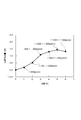
- FIG. 8 shows the result of plotting an example of the improvement amount of the Q value, which is an index indicating the transmission performance of optical communication, with respect to the number of equalization stages, that is, the number of stages N of the digital signal processing circuit.
- the modulation method is polarization multiplexed QPSK
- the bit rate is 43 Gb / s
- 5000 km transmission is performed by the cyclic transmission test
- the continuous optical signal and the received optical signal output from the local oscillation light source 100 in the optical receiver are After mixing, detection was performed by four balanced photon detectors 300A-D.
- each signal of the X polarization I axis, the X polarization Q axis, the Y polarization I axis, and the Y polarization Q axis is analog-to-digital converted by the four analog-digital converters 400A-D, and the digital sampling oscilloscope is used.
- 4 serial data were accumulated at a sampling rate of 40 Gsample / s.
- the equalization ability was confirmed by off-line analysis on a computer.
- the chromatic dispersion amounts of the first, second, third, and fourth stages were ⁇ 900 ps / nm, ⁇ 700 ps / nm, ⁇ 500 ps / nm, and ⁇ 300 ps / nm.
- N 4
- the chromatic dispersion amounts of the first, second, third, fourth, and fifth stages are ⁇ 1000 ps / nm, ⁇ 800 ps / nm, ⁇ 600 ps / nm, ⁇ 400 ps / nm, ⁇ 200 ps / nm.
- the first stage, the second stage, the third stage, the fourth stage, the fifth stage, and the sixth stage have chromatic dispersion amounts of ⁇ 1100 ps / nm, ⁇ 900 ps / nm, ⁇ 700 ps / nm, ⁇ 500 ps / nm, ⁇ 300 ps / nm, and ⁇ 100 ps / nm.
- These setting methods are not optimal and are examples.
Landscapes
- Engineering & Computer Science (AREA)
- Computer Networks & Wireless Communication (AREA)
- Signal Processing (AREA)
- Physics & Mathematics (AREA)
- Nonlinear Science (AREA)
- Electromagnetism (AREA)
- Optical Communication System (AREA)
Abstract
光受信器は、デジタル信号処理集積回路を少なくとも設けた。また、デジタル信号処理集積回路は、4つのデジタル信号に対して、非線形等化デジタル信号処理を適用する非線形等化回路を少なくとも含む。さらに、非線形等化回路は、N段(N≧1)のデジタル信号処理回路で構成され、N段のデジタル信号処理回路のうち、m段目のデジタル信号処理回路は、入力する複素デジタル信号系列dx[m,i]に対し、線形歪みを付加する第1の線形歪み付加部と、複素位相回転を与えられた複素デジタル信号に対して波形歪みを付加することで、第1の線形歪み付加部における波形歪みを除去する第1の線形歪み除去部などを有する。
Description
この発明は、デジタルコヒーレント方式を用いた光伝送システムの光受信器、及びN(N≧1)段のデジタル信号処理回路から構成される非線形等化回路に関するものである。
40Gbit/sや100Gbit/sのような大容量光伝送のためには、光信号対雑音電力限界の克服や高密度波長多重化が課題である。光信号対雑音電力限界を克服する技術として、従来のオンオフキーイング(OOK:On-Off Keying)に対して、2値位相偏移変調(BPSK:Binary Phase-Shift Keying)や4値PSK(QPSK:Quaternary Phase-Shift Keying)の利用が知られている。また、高密度波長多重化のために、直交する2つの偏波成分に独立の信号を割り当てる偏波多重によって、1シンボル当たりの伝送ビット数を2倍に増やす方式や、QPSKや16値直交振幅変調(16QAM:16 Quadrature Amplitude Modulation)のように、信号多重度を上げて、1シンボル当たりの伝送ビット数を増やす方式が知られている。QPSKや16QAMは、光伝送システムの送信側の光送信器において、同位相軸(I軸:In-Phase軸)と、直交位相軸(Q軸:Quadrature-Phase軸)とに信号を割り当てて伝送する。
光信号の検波方式としては、従来、二乗検波方式や遅延検波方式のような直接検波方式が利用されてきた。これらの方式では、光受信器に局部発振光源を持つことなく光信号の検波が可能であり、簡素かつ低コストで光受信器の実装が可能である。一方、光受信器に局部発振光源を持つ同期検波方式にデジタル信号処理を組み合わせて受信するデジタルコヒーレント方式が注目されている(例えば、非特許文献1参照)。
このデジタルコヒーレント方式では、同期検波による線形な光電気変換と、デジタル信号処理による固定的、半固定的及び適応的な線形等化により、光受信器における安定な偏波多重信号の分離や、波形歪みの補償が可能となる。このため、光伝送路で生じる波長分散や偏波モード分散(PMD:Polarization-Mode Dispersion)等に起因する線形な波形歪みに対する優れた等化特性や優れた雑音耐力を実現できる。
図9は、多中継光伝送路の構成例と順方向伝搬の逐次計算方法の概念を示す図である。図9に示すように、光増幅器91が挿入された光ファイバ92中を高い光パワーで伝送する際には、ファイバ非線形光学効果が伝送品質に顕著な劣化をもたらす。光ファイバ中の伝搬は非線形シュレディンガー方程式により記述され、逐次計算法としてスプリット・ステップ・フーリエ法(SSFM:Split-Step Fourier Method)が用いられる。通常、SSFMでは、光伝送路を短区間(多中継システムの1中継区間より十分短い区間)に分割し、伝送損失や波長分散(CD)のような線形効果と、自己位相変調である非線形位相回転(NL)のような非線形効果とを交互に取り込む逐次計算を行う(図9参照)。
ファイバ非線形光学効果による伝送品質劣化を等化する方法として、例えば、非特許文献2に示されるデジタル逆伝搬方式が検討されてきた。図10は、デジタル逆伝搬方式の概念を示す図である。このデジタル逆伝搬方式は、図10に示すように、伝送方向とは逆方向の伝搬計算をSSFMにより行うことにより、送信端での歪みのない光波形を得る方法である。デジタル逆伝搬方式におけるSSFMでは、信号処理にかかる負荷を考慮して、通常、高々、数区間/中継~10区間/中継で信号処理される。このとき、波長分割多重された他のチャネルからの非線形干渉成分を除去することが困難であるため、通常はチャネル内の非線形効果である自己位相変調である非線形位相回転による波形歪みを等化する(図10参照)。
Optical Internetworking Forum, "100G Ultra Long Haul DWDM Framework Document", http://www.oiforum.com/public/documents/OIF-FD-100G-DWDM-01.0.pdf, June 2009.
T.Hoshida, "A question of diminishing returns?", ECOC (European Conference on Optical Communication)2010, Workshop 11,2010.
しかしながら、上記の従来技術(非特許文献2)によれば、SSFMを伝送方向と逆方向に解くため、中継数に比例して回路規模が増大するという問題点があった。
この発明は、上述のような課題を解決するためになされたもので、デジタル逆伝搬方式よりも小さな回路規模と消費電力でファイバ非線形光学効果に起因する波形歪みを等化することができ、伝送品質を向上させることができる光受信器及び非線形等化回路を得ることを目的とする。
この発明に係る光受信器は、受信光信号と同一の中心波長で発振する光信号を生成する局部発振光源と、前記受信光信号と前記局部発振光源から出力される光信号とを混合する偏波ダイバーシチ型の光90度ハイブリッド回路と、前記光90度ハイブリッド回路から出力される4対の光信号を検波する4つのバランス型の光子検出器と、前記4つの光子検出器から出力される4つの電気信号をアナログデジタル変換する4つのアナログデジタル変換器と、前記4つのアナログデジタル変換器に接続されたデジタル信号処理集積回路とを設けた。
また、この発明に係る光受信器のデジタル信号処理集積回路は、4つのデジタル信号に対して、光伝送路の波長分散を補償する波長分散補償回路と、4つのデジタル信号に対して、非線形等化デジタル信号処理を適用する非線形等化回路と、4つのデジタル信号に対して、伝送路の偏波モード分散を補償し、偏波多重信号を分離する適応等化回路と、4つのデジタル信号に対して、前記受信光信号と前記局部発振光源から出力される光信号との間の中心周波数差を補償する搬送波周波数オフセット補償回路と、4つのデジタル信号に対して、前記受信光信号と前記局部発振光源から出力される光信号との間の光位相差を補償する搬送波位相オフセット補償回路とを少なくとも含む。
さらに、この発明に係る光受信器のデジタル信号処理集積回路の非線形等化回路は、N段(N≧1)のデジタル信号処理回路で構成され、前記N段のデジタル信号処理回路のうち、m段目のデジタル信号処理回路は、入力する第1の複素デジタル信号系列dx[m,i]に対し、伝達関数Hpre,x[m](f)の線形歪みを付加する第1の線形歪み付加部と、入力する第2の複素デジタル信号系列dy[m,i]に対し、伝達関数Hpre,y[m](f)の線形歪みを付加する第2の線形歪み付加部と、線形歪みを付加された前記第1の複素デジタル信号系列の絶対値の二乗である、電力Px[m,i]を計算する第1の電力計算部と、線形歪みを付加された前記第2の複素デジタル信号系列の絶対値の二乗である、電力Py[m,i]を計算する第2の電力計算部と、前記電力Px[m,i]の重み付け平均電力Pavg,xx[m,i]=αxx[-a]Px[m,i-a]+αxx[-a+1]Px[m,i-a+1]+・・・+αxx[0]Px[m,i]+・・・+αxx[b]Px[m,i+b]を計算する第1の重み付け平均部と、前記電力Py[m,i]の重み付け平均電力Pavg,xy[m,i]=αxy[-a]Py[m,i-a]+αxy[-a+1]Py[m,i-a+1]+・・・+αxy[0]Py[m,i]+・・・+αxy[b]Py[m,i+b]を計算する第2の重み付け平均部と、前記電力Px[m,i]の重み付け平均電力Pavg,yx[m,i]=αyx[-a]Px[m,i-a]+αyx[-a+1]Px[m,i-a+1]+・・・+αyx[0]Px[m,i]+・・・+αyx[b]Px[m,i+b]を計算する第3の重み付け平均部と、前記電力Py[m,i]の重み付け平均電力Pavg,yy[m,i]=αyy[-a]Py[m,i-a]+αyy[-a+1]Py[m,i-a+1]+・・・+αyy[0]Py[m,i]+・・・+αyy[b]Py[m,i+b]を計算する第4の重み付け平均部と、前記重み付け平均電力Pavg,xx[m,i]に第1の効率γxxを乗算して位相回転量φxx[m,i]=γxx[m,i]Pavg,xx[m,i]を生成する第1の位相回転量生成部と、前記重み付け平均電力Pavg,xy[m,i]に第2の効率γxyを乗算して位相回転量φxy[m,i]=γxy[m,i]Pavg,xy[m,i]を生成する第2の位相回転量生成部と、前記重み付け平均電力Pavg,yx[m,i]に第3の効率γyxを乗算して位相回転量φyx[m,i]=γyx[m,i]Pavg,yx[m,i]を生成する第3の位相回転量生成部と、前記重み付け平均電力Pavg,yy[m,i]に第4の効率γyyを乗算して位相回転量φyy[m,i]=γyy[m,i]Pavg,yy[m,i]を生成する第4の位相回転量生成部と、前記位相回転量φxx[m,i]とφxy[m,i]とを加算して複素位相回転量φx[m,i]=φxx[m,i]+φxy[m,i]を計算する第1の加算部と、前記位相回転量φyx[m,i]とφyy[m,i]とを加算して複素位相回転量φy[m,i]=φyx[m,i]+φyy[m,i]を計算する第2の加算部と、前記複素位相回転量φx[m,i]を複素信号exp(-jφx[m,i])に変換する第1の複素位相回転用信号生成部と、前記複素位相回転量φy[m,i]を複素信号exp(-jφy[m,i])に変換する第2の複素位相回転用信号生成部と、線形歪みを付加された前記第1の複素デジタル信号系列に前記複素信号exp(-jφx[m,i])を乗算することで複素位相回転を与える第1の複素位相回転部と、線形歪みを付加された前記第2の複素デジタル信号系列に前記複素信号exp(-jφy[m,i])を乗算することで複素位相回転を与える第2の複素位相回転部と、前記第1の複素位相回転部により複素位相回転を与えられた複素デジタル信号に対して前記線形な波形歪みの伝達関数Hpre,x[m](f)の逆関数Hpre,x[m]-1(f)もしくは複素共役関数Hpre,x[m]*(f)を伝達関数Hpost,x[m](f)として有する波形歪みを付加することで、前記第1の線形歪み付加部における波形歪みを除去する第1の線形歪み除去部と、前記第2の複素位相回転部により複素位相回転を与えられた複素デジタル信号に対して前記線形な波形歪みの伝達関数Hpre,y[m](f)の逆関数Hpre,y[m]-1(f)もしくは複素共役関数Hpre,y[m]*(f)を伝達関数Hpost,y[m](f)として有する波形歪みを付加することで、前記第2の線形歪み付加部における波形歪みを除去する第2の線形歪み除去部とを有する。
この発明に係る光受信器は、デジタル逆伝搬方式よりも小さな回路規模と消費電力でファイバ非線形光学効果に起因する波形歪みを等化することができ、伝送品質を向上させることができる。
この発明の実施例1について以下説明する。
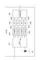
この発明の実施例1に係る光受信器、非線形等化回路及びデジタル信号処理回路について図1から図8までを参照しながら説明する。図1は、この発明の実施例1に係る光受信器の構成を示すブロック図である。なお、各図中、同一符号は同一又は相当部分を示す。
図1において、光受信器は、局部発振光源100と、偏波ダイバーシチ型の光90度ハイブリッド回路200と、4つのバランス型の光子検出器300A、300B、300C、300Dと、4つのアナログデジタル変換器(ADC)400A、400B、400C、400Dと、デジタル信号処理集積回路500とが設けられている。
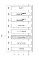
図2は、この発明の実施例1に係る光受信器のデジタル信号処理集積回路の構成を示すブロック図である。
図2において、デジタル信号処理集積回路500は、前処理回路502と、波長分散補償回路503と、非線形等化回路504と、タイミング抽出回路505と、適応等化回路506と、搬送波周波数オフセット補償回路507と、搬送波位相オフセット補償回路508と、識別回路509とが設けられている。
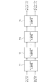
図3は、この発明の実施例1に係る非線形等化回路の構成を示すブロック図である。
図3において、非線形等化回路504は、N段(N≧1)のデジタル信号処理回路で構成され、1段目のデジタル信号処理回路11と、2段目のデジタル信号処理回路12と、m(m<N)段目のデジタル信号処理回路1mと、N段目のデジタル信号処理回路1Nとが設けられている。
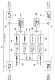
図4は、この発明の実施例1に係るデジタル信号処理回路の構成を示すブロック図である。この図4は、非線形等化回路504を構成するN段のデジタル信号処理回路のうち、1段分(m段目)を示す。
図4において、デジタル信号処理回路1mは、2つの波長分散付加部1A、1Bと、2つの電力計算部2A、2Bと、4つの重み付け平均部3A、3B、3C、3Dと、4つの効率乗算部4A、4B、4C、4Dと、2つの加算部5A、5Bと、2つの複素位相回転用信号生成部6A、6Bと、2つの複素位相回転部7A、7Bと、2つの波長分散除去部8A、8Bとが設けられている。
なお、波長分散付加部1A、1Bや、波長分散除去部8A、8Bは、時間領域もしくは周波数領域での有限長インパルス応答フィルタにより実現可能である。
また、N≧2の場合、m段目の波長分散除去部8A(波長分散付加量pxとする)とm+1段目の波長分散付加部1A(波長分散付加量qxとする)とは、あえて2つの機能ブロックに分割せず、波長分散付加量px+qxの単一の波長分散付加部としてもよい。同様に、m段目の波長分散除去部8B(波長分散付加量pyとする)とm+1段目の波長分散付加部1B(波長分散付加量qyとする)とは、あえて2つの機能ブロックに分割せず、波長分散付加量py+qyの単一の波長分散付加部としてもよい。すなわち、N段(N≧2)のデジタル信号処理回路のうち、m(m<N)段目のデジタル信号処理回路は、伝達関数Hpost,z[m](f)とHpre,z[m+1](f)で表される2つの線形フィルタ(z∈{x,y})を、単一の線形フィルタHjoint,z[m:m+1](f)として実現してもよい。
つぎに、この実施例1に係る光受信器、非線形等化回路及びデジタル信号処理回路の動作について図面を参照しながら説明する。
図1において、光受信器の局部発振光源100は、図示しない光伝送路から入力される光信号(受信光信号)の中心波長と概略一致した中心波長で発振し、単一波長のCW(Continuous Wave)光信号を生成して、このCW光信号を偏波ダイバーシチ型の光90度ハイブリッド回路200に出力する。
光90度ハイブリッド回路200は、図示しない光伝送路から入力される受信光信号と、局部発振光源100から入力されるCW光信号とを混合し、8通りの干渉を生じさせた光信号を出力する。
すなわち、光90度ハイブリッド回路200は、受信光信号の直交する2つの偏波モード(X/Y)と、受信光信号とCW光信号との間の位相差(0度/180度/90度/270度)について、X偏波(0度)の干渉光信号と、X偏波(180度)の干渉光信号とをバランス型の光子検出器300Aに出力する。
同様に、光90度ハイブリッド回路200は、X偏波(90度)の干渉光信号と、X偏波(270度)の干渉光信号とをバランス型の光子検出器300Bに出力し、Y偏波(0度)の干渉光信号と、Y偏波(180度)の干渉光信号とをバランス型の光子検出器300Cに出力し、Y偏波(90度)の干渉光信号と、Y偏波(270度)の干渉光信号とをバランス型の光子検出器300Dに出力する。
光子検出器300Aは、光90度ハイブリッド回路200から入力されるX偏波(0度)の干渉光信号と、X偏波(180度)の干渉光信号とをそれぞれ二乗検波して電気信号に変換し、各電気信号の差分をアナログデジタル変換器400Aに出力する。
同様に、光子検出器300Bは、光90度ハイブリッド回路200から入力されるX偏波(90度)の干渉光信号と、X偏波(270度)の干渉光信号とをそれぞれ二乗検波し電気信号に変換し、各電気信号の差分をアナログデジタル変換器400Bに出力する。また、光子検出器300Cは、光90度ハイブリッド回路200から入力されるY偏波(0度)の干渉光信号と、Y偏波(180度)の干渉光信号とをそれぞれ二乗検波し電気信号に変換し、各電気信号の差分をアナログデジタル変換器400Cに出力する。さらに、光子検出器300Dは、光90度ハイブリッド回路200から入力されるY偏波(90度)の干渉光信号と、Y偏波(270度)の干渉光信号とをそれぞれ二乗検波し電気信号に変換し、各電気信号の差分をアナログデジタル変換器400Dに出力する。
アナログデジタル変換器400Aは、光子検出器300Aから入力される電気信号をサンプリングすることで離散時間化及び量子化したデジタル信号XIをデジタル信号処理集積回路500に出力する。
同様に、アナログデジタル変換器400Bは、光子検出器300Bから入力される電気信号をサンプリングすることで離散時間化及び量子化したデジタル信号XQをデジタル信号処理集積回路500に出力する。また、アナログデジタル変換器400Cは、光子検出器300Cから入力される電気信号をサンプリングすることで離散時間化及び量子化したデジタル信号YIをデジタル信号処理集積回路500に出力する。さらに、アナログデジタル変換器400Dは、光子検出器300Dから入力される電気信号をサンプリングすることで離散時間化及び量子化したデジタル信号YQをデジタル信号処理集積回路500に出力する。
図2において、デジタル信号処理集積回路500の前処理回路502は、アナログデジタル変換器400Aから入力されるデジタル信号XI、アナログデジタル変換器400Bから入力されるデジタル信号XQ、アナログデジタル変換器400Cから入力されるデジタル信号YI、アナログデジタル変換器400Dから入力されるデジタル信号YQに対して、4つのデジタル信号の振幅ばらつきを抑圧するための振幅正規化や、遅延差補正のためのデスキュー等の前処理を行い、処理後の4つのデジタル信号を波長分散補償回路503に出力する。
波長分散補償回路503は、前処理回路502から入力される4つのデジタル信号に対して、時間領域等化若しくは周波数領域等化による線形波形等化を行うことで、伝送路で生じる波長分散を概略100%補償し、波長分散補償後の4つのデジタル信号を非線形等化回路504に出力する。
非線形等化回路504は、波長分散補償回路503から入力される4つのデジタル信号(2対の複素信号とみなす)に対して後述する非線形等化デジタル信号処理を適用し、非線形等化後の4つのデジタル信号(2対の複素信号とみなす)をタイミング抽出回路505に出力する。
タイミング抽出回路505は、非線形等化回路504から入力される4つのデジタル信号に対して識別タイミングの抽出を適応的に行い、アナログデジタル変換器400A~400Dのサンプリングタイミングをフィードバック制御することで、オーバサンプリング比2倍のサンプリングレートの4つのデジタルデータを適応等化回路506に出力する。
適応等化回路506は、タイミング抽出回路505から入力される4つのデジタル信号に対して、包絡線一定化規範のようなアルゴリズムを用いて、偏波多重分離を適応的に行い、なおかつ、伝送路のPMD(偏波モード分散)等を補償した4つのデジタル信号を搬送波周波数オフセット補償回路507に出力する。
搬送波周波数オフセット補償回路507は、適応等化回路506から入力される4つのデジタル信号における、局部発振光源100から出力されるCW光信号と受信光信号との中心周波数差を補償し、補償後の4つのデジタル信号を搬送波位相オフセット補償回路508に出力する。
搬送波位相オフセット補償回路508は、搬送波周波数オフセット補償回路507から入力される4つのデジタル信号に対して、X偏波成分とY偏波成分それぞれについて信号点がI軸及びQ軸を軸とする複素平面において、信号点が45度、135度、-45度、-135度の4点に概略収束するよう、適応的に位相オフセット補償を行い、位相オフセット補償後のデジタル信号を識別回路509に出力する。
識別回路509は、搬送波位相オフセット補償回路508から入力される4つのデジタル信号に対して2値識別を行い、識別後の4つの2値信号を図示しない外部に出力する。
図3において、N段(N≧1)のデジタル信号処理回路で構成された非線形等化回路504の1段目のデジタル信号処理回路11は、波長分散補償回路503から複素デジタル信号dx[0]=Exi[0]+jExq[0]と、dy[0]=Eyi[0]+jEyq[0]が入力され、1段分の非線形等化を行った後に、等化後の複素デジタル信号d’x[0]=E’xi[0]+jE’xq[0]と、d’y[0]=E’yi[0]+jE’yq[0]を2段目のデジタル信号処理回路12に出力する。
2段目のデジタル信号処理回路12は、1段目のデジタル信号処理回路11から複素デジタル信号dx[1](=d’x[0])と、dy[1](=d’y[0])が入力され、1段分の非線形等化を行った後に、等化後の複素デジタル信号d’x[1]=E’xi[1]+jE’xq[1]と、d’y[1]=E’yi[1]+jE’yq[1]を3段目のデジタル信号処理回路(図示せず)に出力する。
m(m<N)段目のデジタル信号処理回路1mは、m-1段目のデジタル信号処理回路(図示せず)から複素デジタル信号dx[m-1](=d’x[m-2])と、dy[m-1](=d’y[m-2])とが入力され、1段分の非線形等化を行った後に、等化後の複素デジタル信号d’x[m-1]=E’xi[m-1]+jE’xq[m-1]と、d’y[m-1]=E’yi[m-1]+jE’yq[m-1]をm+1段目のデジタル信号処理回路(図示せず)に出力する。
N段目のデジタル信号処理回路1Nは、N-1段目のデジタル信号処理回路(図示せず)から複素デジタル信号dx[N-1](=d’x[N-2])と、dy[N-1](=d’y[N-2])が入力され、1段分の非線形等化を行った後に、等化後の複素デジタル信号d’x[N-1]=E’xi[N-1]+jE’xq[N-1]と、d’y[N-1]=E’yi[N-1]+jE’yq[N-1]をタイミング抽出回路505に出力する。
図4において、波長分散付加部1Aは、前段から入力される複素デジタル信号系列dx[m,i]=Exi[m]+jExq[m]に対して波長分散を付加し、複素位相回転部7Aと、電力計算部2Aに出力する。同様に、波長分散付加部1Bは、前段から入力される複素デジタル信号系列dy[m,i]=Eyi[m]+jEyq[m]に対して波長分散を付加し、複素位相回転部7Bと、電力計算部2Bに出力する。例えば、波長分散付加部1A、1Bの波長分散量は-600ps/nmとする。すなわち、第1の線形歪み付加部(波長分散付加部1A)は、入力する複素デジタル信号系列dx[m,i]に対し、伝達関数Hpre,x[m](f)の線形な波形歪みを付加する。同様に、第2の線形歪み付加部(波長分散付加部1B)は、入力する複素デジタル信号系列dy[m,i]に対し、伝達関数Hpre,y[m](f)の線形な波形歪みを付加する。
電力計算部2Aは、波長分散付加部1Aから入力される波長分散付加後の複素デジタル信号系列の絶対値の二乗、すなわち電力Px[m,i]を計算し、重み付け平均部3Aと、重み付け平均部3Cに出力する。同様に、電力計算部2Bは、波長分散付加部1Bから入力される波長分散付加後の複素デジタル信号系列の絶対値の二乗、すなわち電力Py[m,i]を計算し、重み付け平均部3Bと、重み付け平均部3Dに出力する。
重み付け平均部3Aは、電力Px[m,i]について、その重み付け平均電力Pavg,xx[m,i]=αxx[-a]Px[m,i-a]+αxx[-a+1]Px[m,i-a+1]+・・・+αxx[0]Px[m,i]+・・・+αxx[b]Px[m,i+b]を計算し、Pavg,xx[m,i]を効率乗算部4Aに出力する。αxx[-a],αxx[-a+1],αxx[b]が重みに相当する。
重み付け平均部3Bは、電力Py[m,i]について、その重み付け平均電力Pavg,xy[m,i]=αxy[-a]Py[m,i-a]+αxy[-a+1]Py[m,i-a+1]+・・・+αxy[0]Py[m,i]+・・・+αxy[b]Py[m,i+b]を計算し、Pavg,xy[m,i]を効率乗算部4Bに出力する。αxy[-a],αxy[-a+1],αxy[b]が重みに相当する。
重み付け平均部3Cは、電力Px[m,i]について、その重み付け平均電力Pavg,yx[m,i]=αyx[-a]Px[m,i-a]+αyx[-a+1]Px[m,i-a+1]+・・・+αyx[0]Px[m,i]+・・・+αyx[b]Px[m,i+b]を計算し、Pavg,yx[m,i]を効率乗算部4Cに出力する。αyx[-a],αyx[-a+1],αyx[b]が重みに相当する。
重み付け平均部3Dは、電力Py[m,i]について、その重み付け平均電力Pavg,yy[m,i]=αyy[-a]Py[m,i-a]+αyy[-a+1]Py[m,i-a+1]+・・・+αyy[0]Py[m,i]+・・・+αyy[b]Py[m,i+b]を計算し、Pavg,yy[m,i]を効率乗算部4Dに出力する。αyy[-a],αyy[-a+1],αyy[b]が重みに相当する。
平均区間-a~bは、例えばa=b=4とし、重みは、例えばαxx[-a]=αxx[-a+1]=・・・=αxx[b]=1/9、αxy[-a]=αxy[-a+1]=・・・=αxy[b]=1/9、αyx[-a]=αyx[-a+1]=・・・=αyx[b]=1/9、αyy[-a]=αyy[-a+1]=・・・=αyy[b]=1/9とすればよい。
効率乗算部4Aは、重み付け平均部3Aから入力される重み付け平均電力Pavg,xx[m,i]に非線形位相回転効率γxx[m]を乗算し、乗算結果φxx[m,i]=γxx[m]Pavg,xx[m,i]を加算部5Aに出力する。
効率乗算部4Bは、重み付け平均部3Bから入力される重み付け平均電力Pavg,xy[m,i]に非線形位相回転効率γxy[m]を乗算し、乗算結果φxy[m,i]=γxy[m]Pavg,xy[m,i]を加算部5Aに出力する。
効率乗算部4Cは、重み付け平均部3Cから入力される重み付け平均電力Pavg,yx[m,i]に非線形位相回転効率γyx[m]を乗算し、乗算結果φyx[m,i]=γyx[m]Pavg,yx[m,i]を加算部5Bに出力する。
効率乗算部4Dは、重み付け平均部3Dから入力される重み付け平均電力Pavg,yy[m,i]に非線形位相回転効率γyy[m]を乗算し、乗算結果φyy[m,i]=γyy[m]Pavg,yy[m,i]を加算部5Bに出力する。
すなわち、第1の位相回転量生成部(効率乗算部4A)は、重み付け平均電力Pavg,xx[m,i]に第1の効率γxxを乗算して位相回転量φxx[m,i]=γxx[m,i]Pavg,xx[m,i]を生成する。また、第2の位相回転量生成部(効率乗算部4B)は、重み付け平均電力Pavg,xy[m,i]に第2の効率γxyを乗算して位相回転量φxy[m,i]=γxy[m,i]Pavg,xy[m,i]を生成する。また、第3の位相回転量生成部(効率乗算部4C)は、重み付け平均電力Pavg,yx[m,i]に第3の効率γyxを乗算して位相回転量φyx[m,i]=γyx[m,i]Pavg,yx[m,i]を生成する。さらに、第4の位相回転量生成部(効率乗算部4D)は、重み付け平均電力Pavg,yy[m,i]に第4の効率γyyを乗算して位相回転量φyy[m,i]=γyy[m,i]Pavg,yy[m,i]を生成する。
加算部5Aは、重み付け平均部4Aから入力される非線形位相回転量φxx[m,i]と、重み付け平均部4Bから入力される非線形位相回転量φxy[m,i]との加算を行い、加算結果φx[m,i]=φxx[m,i]+φxy[m,i]を複素位相回転用信号生成部6Aに出力する。同様に、加算部5Bは、重み付け平均部4Cから入力される非線形位相回転量φyx[m,i]と、重み付け平均部4Dから入力される非線形位相回転量φyy[m,i]との加算を行い、加算結果φy[m,i]=φyx[m,i]+φyy[m,i]を複素位相回転用信号生成部6Bに出力する。
複素位相回転用信号生成部6Aは、加算部5Aから入力されるφx[m,i]を複素信号exp(-jφx[m,i])に変換して複素位相回転部7Aに出力する。同様に、複素位相回転用信号生成部6Bは、加算部5Bから入力されるφy[m,i]を複素信号exp(-jφy[m,i])に変換して複素位相回転部7に出力する。
複素位相回転部7Aは、波長分散付加部1Aから入力される波長分散を付加された複素デジタル信号系列と、複素位相回転用信号生成部6Aから入力される複素信号exp(-jφx[m,i])との乗算を行うことで、伝送路の非線形位相回転の逆演算を行い、演算後の信号を波長分散除去部8Aに出力する。同様に、複素位相回転部7Bは、波長分散付加部1Bから入力される波長分散を付加された複素デジタル信号系列と、複素位相回転用信号生成部6Bから入力される複素信号exp(-jφy[m,i])との乗算を行うことで、伝送路の非線形位相回転の逆演算を行い、演算後の複素デジタル信号を波長分散除去部8Bに出力する。
波長分散除去部8Aは、複素位相回転部7Aから入力される複素デジタル信号に、波長分散付加部1Aで付加した波長分散を除去するよう、逆極性の波長分散を与え、波長分散付加後の複素デジタル信号d’x「m」=E’xi[m]+jE’xq[m]を次段に出力する。同様に、波長分散除去部8Bは、複素位相回転部7Bから入力される複素デジタル信号に、波長分散付加部1Bで付加した波長分散を除去するよう、逆極性の波長分散を与え、波長分散付加後の複素デジタル信号d’y「m」=E’yi[m]+jE’yq[m]を次段に出力する。
すなわち、第1の線形歪み除去部(波長分散除去部8A)は、複素位相回転部7Aにより複素位相回転を与えられた複素デジタル信号に対して線形な波形歪みの伝達関数Hpre,x[m](f)の逆関数Hpre,x[m]-1(f)もしくは複素共役関数Hpre,x[m]*(f)を伝達関数Hpost,x[m](f)として有する波形歪みを付加することで、第1の線形歪み付加部における波形歪みを除去する。同様に、第2の線形歪み除去部(波長分散除去部8B)は、複素位相回転部7Bにより複素位相回転を与えられた複素デジタル信号に対して線形な波形歪みの伝達関数Hpre,y[m](f)の逆関数Hpre,y[m]-1(f)もしくは複素共役関数Hpre,y[m]*(f)を伝達関数Hpost,y[m](f)として有する波形歪みを付加することで、第2の線形歪み付加部における波形歪みを除去する。
例えば、波長分散付加部1A及び波長分散付加部1Bで-600ps/nmの波長分散を付加していた場合、波長分散除去部8A及び波長分散除去部8Bは、+600ps/nmの波長分散を付加する。
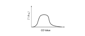
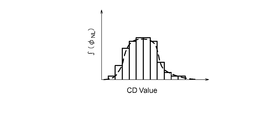
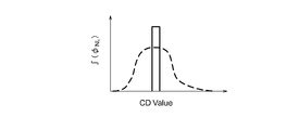
図5A、図5B及び図5Cは、この発明の実施例1に係るデジタル信号処理回路の波長分散値と積算された非線形位相回転量との関係及びその簡略化を示す図である。また、図6は、この発明の実施例1に係る非線形等化回路の非線形等化の概念を示す図である。
この発明の実施例1に係るデジタル信号処理回路では、ある特定の符号間干渉条件(例えば、特定の波長分散値CD[i])において与えられた非線形位相回転量の積算値(∫φNL[i])をそれぞれ補償する。最も正確には、図5Aのように、波長分散値(横軸:CD Value)と積算非線形位相回転量(縦軸:∫φNL)との関係が得られる。実際上は、図5Bに示すように離散化が可能であり、最も簡単には、図5Cに示すように、単一の波長分散値で代表させることも可能である。むろん、波長分散値の離散化の度合いが大きくなると等化能力が低下する。
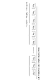
上記の概念に基づき、図6に示される非線形等化回路を構成するデジタル信号処理回路のブロック構成により、簡易に非線形等化を行うことが可能である。ある特定の符号間干渉条件を作り出すために、まず、波長分散値CDaを付加してパルスを広げ、非線形位相回転(非線形位相回転量:φNLa)を与え、波長分散値-CDaを付加して事前に広げたパルスを元に戻す。これを1段とし、同様のデジタル信号処理回路を複数段設けることで非線形等化を実現する。この方法によれば、デジタル逆伝搬方式のように、1中継区間を複数区間に分割し、全中継区間をSSFM(スプリット・ステップ・フーリエ法)により逆方向伝搬する必要がない。非線形な伝送過程を忠実に再現することが不可能であり、等化能力ではやや劣る可能性があるが、デジタル信号処理回路を大幅に簡素化できる可能性がある。
ここで、光受信器のデジタル信号処理集積回路500の機能を計算機でシミュレートし、非線形等化回路504の等化段数依存性について図7及び図8を参照しながら説明する。
図7は、この発明の実施例1に係る光受信器のデジタル信号処理集積回路の機能をシミュレートした構成を示すブロック図である。また、図8は、この発明の実施例1に係る非線形等化回路の等化段数依存性を示す図である。
この図7は、オフライン解析に用いたデジタル信号処理集積回路500全体の機能ブロック構成を示す。レート変換部501と、前処理部502Aと、波長分散補償部503Aと、非線形等化部504Aと、タイミング抽出部505Aと、適応等化部506Aと、搬送波周波数オフセット補償部507Aと、搬送波位相オフセット補償部508Aと、識別部509Aと、Q値計算部510とが設けられている。以下、各部の動作について説明する。
レート変換部501は、図示しない外部(デジタルサンプリングオシロスコープでの取得データ)から入力される4つのデジタル信号を、43Gb/sのビットレートに同期した速度にサンプリングレート変換し、レート変換後の4つのデジタル信号を前処理部502Aに出力した。
前処理部502Aは、4つのデジタル信号の振幅ばらつきを抑圧するための振幅正規化や、遅延差補正のためのデスキュー等の前処理を行い、処理後の4つのデジタル信号を波長分散補償部503Aに出力した。
波長分散補償部503Aは、前処理部502Aから入力される4つのデジタル信号に対して伝送路で生じた波長分散を補償し、波長分散補償後の4つのデジタル信号を非線形等化部504Aに出力した。
非線形等化部504Aは、波長分散補償部503Aから入力される4つのデジタル信号(2対の複素信号とみなす)に対して、非線形等化回路504の処理に相当する非線形等化デジタル信号処理を適用し、非線形等化後の4つのデジタル信号(2対の複素信号とみなす)をタイミング抽出部505Aに出力した。
タイミング抽出部505Aは、非線形等化部504Aから入力される4つのデジタル信号に対して識別タイミングの抽出を適応的に行い、オーバサンプリング比2倍のサンプリングレートの4つのデジタルデータを適応等化部506Aに出力した。
適応等化部506Aは、タイミング抽出部505Aから入力される4つのデジタル信号に対して、包絡線一定化規範のようなアルゴリズムを用いて、偏波多重分離を適応的に行い、なおかつ、伝送路のPMD等を補償した4つのデジタル信号を搬送波周波数オフセット補償部507Aに出力した。
搬送波周波数オフセット補償部507Aは、適応等化部506Aから入力される4つのデジタル信号における、局部発振光源100から出力される連続光信号と受信光信号との中心周波数差を補償し、補償後の4つのデジタル信号を搬送波位相オフセット補償部508Aに出力した。
搬送波位相オフセット補償部508Aは、搬送波周波数オフセット補償部507Aから入力される4つのデジタル信号に対して、X偏波成分とY偏波成分それぞれについて信号点がI軸及びQ軸を軸とする複素平面において、信号点が45度、135度、-45度、-135度の4点に概略収束するよう、適応的に位相オフセット補償を行い、位相オフセット補償後のデジタル信号を識別部509Aに出力した。
識別部509Aは、搬送波位相オフセット補償部508Aから入力される4つのデジタル信号に対して2値識別を行い、識別後の4つの2値信号をQ値計算部510に出力した。
Q値計算部510は、識別部509Aから入力される4つの2値信号の符号誤り率を計算し、光通信における伝送性能の指標であるQ値を計算した。
図8は、等化段数、つまり、デジタル信号処理回路の段数Nに対して、光通信の伝送性能を示す指標であるQ値の改善量の例をプロットした結果を示す。変調方式を偏波多重QPSKとし、ビットレートを43Gb/sとし、周回伝送試験により5000km伝送を行った場合について、光受信器において局部発振光源100から出力される連続光信号と受信光信号とを混合した後に4つのバランス型の光子検出器300A-Dで検波した。次に、X偏波I軸、X偏波Q軸、Y偏波I軸、Y偏波Q軸の各信号を、4つのアナログデジタル変換器400A-Dでアナログデジタル変換し、デジタルサンプリングオシロスコープにより、40Gsample/sのサンプリングレートで4つのシリアルデータを蓄積した。そして、計算機上でオフライン解析することにより等化能力を確認した。図8の横軸において、段数N=0は非線形等化を行わない場合であり、1段、2段、・・・と段数Nを増やすごとにQ値改善量が増える。
段数Nがそれぞれの場合における付加又は除去する波長分散量は、X偏波とY偏波で同一の値に設定した。また、波長分散付加部1A、1Bで付加される波長分散値Xに対して、波長分散除去部8A、8Bで付加される波長分散値を-Xとした。
N=1の場合、波長分散量を-600ps/nmとした。N=2の場合、1段目、2段目の波長分散量を-700ps/nm、-500ps/nmとした。N=3の場合、1段目、2段目、3段目の波長分散量を-800ps/nm、-600ps/nm、-400ps/nmとした。
N=4の場合、1段目、2段目、3段目、4段目の波長分散量を-900ps/nm、-700ps/nm、-500ps/nm、-300ps/nmとした。N=5の場合、1段目、2段目、3段目、4段目、5段目の波長分散量を-1000ps/nm、-800ps/nm、-600ps/nm、-400ps/nm、-200ps/nmとした。N=6の場合、1段目、2段目、3段目、4段目、5段目、6段目の波長分散量を-1100ps/nm、-900ps/nm、-700ps/nm、-500ps/nm、-300ps/nm、-100ps/nmとした。これらの設定方法が最適という訳ではなく、一例である。
それぞれの場合における効率は、以下のように設定した。効率γxx[m]=γyy[m]=const/N、γxy[m]=γyx[0]=0とした(const:定数)。これらの設定方法が最適という訳ではなく、一例である。
以上の設定により、図8に示すように、N=5の場合にQ値改善量1.5dBが得られた。
1A、1B 波長分散付加部、2A、2B 電力計算部、3A、3B、3C、3D 重み付け平均部、4A、4B、4C、4D 効率乗算部、5A、5B 加算部、6A、6B 複素位相回転用信号生成部、7A、7B 複素位相回転部、8A、8B 波長分散除去部、11、12、1m、1N デジタル信号処理回路、100 局部発振光源、200 光90度ハイブリッド回路、300A、300B、300C、300D 光子検出器、400A、400B、400C、400D アナログデジタル変換器、500 デジタル信号処理集積回路、502 前処理回路、503 波長分散補償回路、504 非線形等化回路、505 タイミング抽出回路、506 適応等化回路、507 搬送波周波数オフセット補償回路、508 搬送波位相オフセット補償回路、509 識別回路。
Claims (5)
- 受信光信号と同一の中心波長で発振する光信号を生成する局部発振光源と、
前記受信光信号と前記局部発振光源から出力される光信号とを混合する偏波ダイバーシチ型の光90度ハイブリッド回路と、
前記光90度ハイブリッド回路から出力される4対の光信号を検波する4つのバランス型の光子検出器と、
前記4つの光子検出器から出力される4つの電気信号をアナログデジタル変換する4つのアナログデジタル変換器と、
前記4つのアナログデジタル変換器に接続されたデジタル信号処理集積回路とを備えた光受信器であって、
前記デジタル信号処理集積回路は、
4つのデジタル信号に対して、光伝送路の波長分散を補償する波長分散補償回路と、
4つのデジタル信号に対して、非線形等化デジタル信号処理を適用する非線形等化回路と、
4つのデジタル信号に対して、伝送路の偏波モード分散を補償し、偏波多重信号を分離する適応等化回路と、
4つのデジタル信号に対して、前記受信光信号と前記局部発振光源から出力される光信号との間の中心周波数差を補償する搬送波周波数オフセット補償回路と、
4つのデジタル信号に対して、前記受信光信号と前記局部発振光源から出力される光信号との間の光位相差を補償する搬送波位相オフセット補償回路とを少なくとも含み、
前記非線形等化回路は、
N段(N≧1)のデジタル信号処理回路で構成され、
前記N段のデジタル信号処理回路のうち、m段目のデジタル信号処理回路は、
入力する第1の複素デジタル信号系列dx[m,i]に対し、伝達関数Hpre,x[m](f)の線形歪みを付加する第1の線形歪み付加部と、
入力する第2の複素デジタル信号系列dy[m,i]に対し、伝達関数Hpre,y[m](f)の線形歪みを付加する第2の線形歪み付加部と、
線形歪みを付加された前記第1の複素デジタル信号系列の絶対値の二乗である、電力Px[m,i]を計算する第1の電力計算部と、
線形歪みを付加された前記第2の複素デジタル信号系列の絶対値の二乗である、電力Py[m,i]を計算する第2の電力計算部と、
前記電力Px[m,i]の重み付け平均電力Pavg,xx[m,i]=αxx[-a]Px[m,i-a]+αxx[-a+1]Px[m,i-a+1]+・・・+αxx[0]Px[m,i]+・・・+αxx[b]Px[m,i+b]を計算する第1の重み付け平均部と、
前記電力Py[m,i]の重み付け平均電力Pavg,xy[m,i]=αxy[-a]Py[m,i-a]+αxy[-a+1]Py[m,i-a+1]+・・・+αxy[0]Py[m,i]+・・・+αxy[b]Py[m,i+b]を計算する第2の重み付け平均部と、
前記電力Px[m,i]の重み付け平均電力Pavg,yx[m,i]=αyx[-a]Px[m,i-a]+αyx[-a+1]Px[m,i-a+1]+・・・+αyx[0]Px[m,i]+・・・+αyx[b]Px[m,i+b]を計算する第3の重み付け平均部と、
前記電力Py[m,i]の重み付け平均電力Pavg,yy[m,i]=αyy[-a]Py[m,i-a]+αyy[-a+1]Py[m,i-a+1]+・・・+αyy[0]Py[m,i]+・・・+αyy[b]Py[m,i+b]を計算する第4の重み付け平均部と、
前記重み付け平均電力Pavg,xx[m,i]に第1の効率γxxを乗算して位相回転量φxx[m,i]=γxx[m,i]Pavg,xx[m,i]を生成する第1の位相回転量生成部と、
前記重み付け平均電力Pavg,xy[m,i]に第2の効率γxyを乗算して位相回転量φxy[m,i]=γxy[m,i]Pavg,xy[m,i]を生成する第2の位相回転量生成部と、
前記重み付け平均電力Pavg,yx[m,i]に第3の効率γyxを乗算して位相回転量φyx[m,i]=γyx[m,i]Pavg,yx[m,i]を生成する第3の位相回転量生成部と、
前記重み付け平均電力Pavg,yy[m,i]に第4の効率γyyを乗算して位相回転量φyy[m,i]=γyy[m,i]Pavg,yy[m,i]を生成する第4の位相回転量生成部と、
前記位相回転量φxx[m,i]とφxy[m,i]とを加算して複素位相回転量φx[m,i]=φxx[m,i]+φxy[m,i]を計算する第1の加算部と、
前記位相回転量φyx[m,i]とφyy[m,i]とを加算して複素位相回転量φy[m,i]=φyx[m,i]+φyy[m,i]を計算する第2の加算部と、
前記複素位相回転量φx[m,i]を複素信号exp(-jφx[m,i])に変換する第1の複素位相回転用信号生成部と、
前記複素位相回転量φy[m,i]を複素信号exp(-jφy[m,i])に変換する第2の複素位相回転用信号生成部と、
線形歪みを付加された前記第1の複素デジタル信号系列に前記複素信号exp(-jφx[m,i])を乗算することで複素位相回転を与える第1の複素位相回転部と、
線形歪みを付加された前記第2の複素デジタル信号系列に前記複素信号exp(-jφy[m,i])を乗算することで複素位相回転を与える第2の複素位相回転部と、
前記第1の複素位相回転部により複素位相回転を与えられた複素デジタル信号に対して前記線形な波形歪みの伝達関数Hpre,x[m](f)の逆関数Hpre,x[m]-1(f)もしくは複素共役関数Hpre,x[m]*(f)を伝達関数Hpost,x[m](f)として有する波形歪みを付加することで、前記第1の線形歪み付加部における波形歪みを除去する第1の線形歪み除去部と、
前記第2の複素位相回転部により複素位相回転を与えられた複素デジタル信号に対して前記線形な波形歪みの伝達関数Hpre,y[m](f)の逆関数Hpre,y[m]-1(f)もしくは複素共役関数Hpre,y[m]*(f)を伝達関数Hpost,y[m](f)として有する波形歪みを付加することで、前記第2の線形歪み付加部における波形歪みを除去する第2の線形歪み除去部とを有する、
光受信器。 - 前記非線形等化回路は、
N段(N≧2)のデジタル信号処理回路で構成され、
前記N段のデジタル信号処理回路のうち、m(m<N)段目のデジタル信号処理回路は、
伝達関数Hpost,z[m](f)とHpre,z[m+1](f)で表される2つの線形フィルタ(z∈{x,y})を、単一の線形フィルタHjoint,z[m:m+1](f)として実現する
請求項1記載の光受信器。 - N段(N≧1)のデジタル信号処理回路で構成された非線形等化回路であって、
前記N段のデジタル信号処理回路のうち、m段目のデジタル信号処理回路は、
入力する第1の複素デジタル信号系列dx[m,i]に対し、伝達関数Hpre,x[m](f)の線形歪みを付加する第1の線形歪み付加部と、
入力する第2の複素デジタル信号系列dy[m,i]に対し、伝達関数Hpre,y[m](f)の線形歪みを付加する第2の線形歪み付加部と、
線形歪みを付加された前記第1の複素デジタル信号系列の絶対値の二乗である、電力Px[m,i]を計算する第1の電力計算部と、
線形歪みを付加された前記第2の複素デジタル信号系列の絶対値の二乗である、電力Py[m,i]を計算する第2の電力計算部と、
前記電力Px[m,i]の重み付け平均電力Pavg,xx[m,i]=αxx[-a]Px[m,i-a]+αxx[-a+1]Px[m,i-a+1]+・・・+αxx[0]Px[m,i]+・・・+αxx[b]Px[m,i+b]を計算する第1の重み付け平均部と、
前記電力Py[m,i]の重み付け平均電力Pavg,xy[m,i]=αxy[-a]Py[m,i-a]+αxy[-a+1]Py[m,i-a+1]+・・・+αxy[0]Py[m,i]+・・・+αxy[b]Py[m,i+b]を計算する第2の重み付け平均部と、
前記電力Px[m,i]の重み付け平均電力Pavg,yx[m,i]=αyx[-a]Px[m,i-a]+αyx[-a+1]Px[m,i-a+1]+・・・+αyx[0]Px[m,i]+・・・+αyx[b]Px[m,i+b]を計算する第3の重み付け平均部と、
前記電力Py[m,i]の重み付け平均電力Pavg,yy[m,i]=αyy[-a]Py[m,i-a]+αyy[-a+1]Py[m,i-a+1]+・・・+αyy[0]Py[m,i]+・・・+αyy[b]Py[m,i+b]を計算する第4の重み付け平均部と、
前記重み付け平均電力Pavg,xx[m,i]に第1の効率γxxを乗算して位相回転量φxx[m,i]=γxx[m,i]Pavg,xx[m,i]を生成する第1の位相回転量生成部と、
前記重み付け平均電力Pavg,xy[m,i]に第2の効率γxyを乗算して位相回転量φxy[m,i]=γxy[m,i]Pavg,xy[m,i]を生成する第2の位相回転量生成部と、
前記重み付け平均電力Pavg,yx[m,i]に第3の効率γyxを乗算して位相回転量φyx[m,i]=γyx[m,i]Pavg,yx[m,i]を生成する第3の位相回転量生成部と、
前記重み付け平均電力Pavg,yy[m,i]に第4の効率γyyを乗算して位相回転量φyy[m,i]=γyy[m,i]Pavg,yy[m,i]を生成する第4の位相回転量生成部と、
前記位相回転量φxx[m,i]とφxy[m,i]とを加算して複素位相回転量φx[m,i]=φxx[m,i]+φxy[m,i]を計算する第1の加算部と、
前記位相回転量φyx[m,i]とφyy[m,i]とを加算して複素位相回転量φy[m,i]=φyx[m,i]+φyy[m,i]を計算する第2の加算部と、
前記複素位相回転量φx[m,i]を複素信号exp(-jφx[m,i])に変換する第1の複素位相回転用信号生成部と、
前記複素位相回転量φy[m,i]を複素信号exp(-jφy[m,i])に変換する第2の複素位相回転用信号生成部と、
線形歪みを付加された前記第1の複素デジタル信号系列に前記複素信号exp(-jφx[m,i])を乗算することで複素位相回転を与える第1の複素位相回転部と、
線形歪みを付加された前記第2の複素デジタル信号系列に前記複素信号exp(-jφy[m,i])を乗算することで複素位相回転を与える第2の複素位相回転部と、
前記第1の複素位相回転部により複素位相回転を与えられた複素デジタル信号に対して前記線形な波形歪みの伝達関数Hpre,x[m](f)の逆関数Hpre,x[m]-1(f)もしくは複素共役関数Hpre,x[m]*(f)を伝達関数Hpost,x[m](f)として有する波形歪みを付加することで、前記第1の線形歪み付加部における波形歪みを除去する第1の線形歪み除去部と、
前記第2の複素位相回転部により複素位相回転を与えられた複素デジタル信号に対して前記線形な波形歪みの伝達関数Hpre,y[m](f)の逆関数Hpre,y[m]-1(f)もしくは複素共役関数Hpre,y[m]*(f)を伝達関数Hpost,y[m](f)として有する波形歪みを付加することで、前記第2の線形歪み付加部における波形歪みを除去する第2の線形歪み除去部とを有する、
非線形等化回路。 - N段(N≧2)のデジタル信号処理回路で構成された非線形等化回路であって、
前記N段のデジタル信号処理回路のうち、m(m<N)段目のデジタル信号処理回路は、
伝達関数Hpost,z[m](f)とHpre,z[m+1](f)で表される2つの線形フィルタ(z∈{x,y})を、単一の線形フィルタHjoint,z[m:m+1](f)として実現する
請求項3記載の非線形等化回路。 - 入力する第1の複素デジタル信号系列dx[m,i]に対し、伝達関数Hpre,x[m](f)の線形歪みを付加する第1の線形歪み付加部と、
入力する第2の複素デジタル信号系列dy[m,i]に対し、伝達関数Hpre,y[m](f)の線形歪みを付加する第2の線形歪み付加部と、
線形歪みを付加された前記第1の複素デジタル信号系列の絶対値の二乗である、電力Px[m,i]を計算する第1の電力計算部と、
線形歪みを付加された前記第2の複素デジタル信号系列の絶対値の二乗である、電力Py[m,i]を計算する第2の電力計算部と、
前記電力Px[m,i]の重み付け平均電力Pavg,xx[m,i]=αxx[-a]Px[m,i-a]+αxx[-a+1]Px[m,i-a+1]+・・・+αxx[0]Px[m,i]+・・・+αxx[b]Px[m,i+b]を計算する第1の重み付け平均部と、
前記電力Py[m,i]の重み付け平均電力Pavg,xy[m,i]=αxy[-a]Py[m,i-a]+αxy[-a+1]Py[m,i-a+1]+・・・+αxy[0]Py[m,i]+・・・+αxy[b]Py[m,i+b]を計算する第2の重み付け平均部と、
前記電力Px[m,i]の重み付け平均電力Pavg,yx[m,i]=αyx[-a]Px[m,i-a]+αyx[-a+1]Px[m,i-a+1]+・・・+αyx[0]Px[m,i]+・・・+αyx[b]Px[m,i+b]を計算する第3の重み付け平均部と、
前記電力Py[m,i]の重み付け平均電力Pavg,yy[m,i]=αyy[-a]Py[m,i-a]+αyy[-a+1]Py[m,i-a+1]+・・・+αyy[0]Py[m,i]+・・・+αyy[b]Py[m,i+b]を計算する第4の重み付け平均部と、
前記重み付け平均電力Pavg,xx[m,i]に第1の効率γxxを乗算して位相回転量φxx[m,i]=γxx[m,i]Pavg,xx[m,i]を生成する第1の位相回転量生成部と、
前記重み付け平均電力Pavg,xy[m,i]に第2の効率γxyを乗算して位相回転量φxy[m,i]=γxy[m,i]Pavg,xy[m,i]を生成する第2の位相回転量生成部と、
前記重み付け平均電力Pavg,yx[m,i]に第3の効率γyxを乗算して位相回転量φyx[m,i]=γyx[m,i]Pavg,yx[m,i]を生成する第3の位相回転量生成部と、
前記重み付け平均電力Pavg,yy[m,i]に第4の効率γyyを乗算して位相回転量φyy[m,i]=γyy[m,i]Pavg,yy[m,i]を生成する第4の位相回転量生成部と、
前記位相回転量φxx[m,i]とφxy[m,i]とを加算して複素位相回転量φx[m,i]=φxx[m,i]+φxy[m,i]を計算する第1の加算部と、
前記位相回転量φyx[m,i]とφyy[m,i]とを加算して複素位相回転量φy[m,i]=φyx[m,i]+φyy[m,i]を計算する第2の加算部と、
前記複素位相回転量φx[m,i]を複素信号exp(-jφx[m,i])に変換する第1の複素位相回転用信号生成部と、
前記複素位相回転量φy[m,i]を複素信号exp(-jφy[m,i])に変換する第2の複素位相回転用信号生成部と、
線形歪みを付加された前記第1の複素デジタル信号系列に前記複素信号exp(-jφx[m,i])を乗算することで複素位相回転を与える第1の複素位相回転部と、
線形歪みを付加された前記第2の複素デジタル信号系列に前記複素信号exp(-jφy[m,i])を乗算することで複素位相回転を与える第2の複素位相回転部と、
前記第1の複素位相回転部により複素位相回転を与えられた複素デジタル信号に対して前記線形な波形歪みの伝達関数Hpre,x[m](f)の逆関数Hpre,x[m]-1(f)もしくは複素共役関数Hpre,x[m]*(f)を伝達関数Hpost,x[m](f)として有する波形歪みを付加することで、前記第1の線形歪み付加部における波形歪みを除去する第1の線形歪み除去部と、
前記第2の複素位相回転部により複素位相回転を与えられた複素デジタル信号に対して前記線形な波形歪みの伝達関数Hpre,y[m](f)の逆関数Hpre,y[m]-1(f)もしくは複素共役関数Hpre,y[m]*(f)を伝達関数Hpost,y[m](f)として有する波形歪みを付加することで、前記第2の線形歪み付加部における波形歪みを除去する第2の線形歪み除去部と
を有するデジタル信号処理回路。
Priority Applications (2)
| Application Number | Priority Date | Filing Date | Title |
|---|---|---|---|
| JP2012557753A JP5523591B2 (ja) | 2011-02-18 | 2011-02-18 | 光受信器、非線形等化回路及びデジタル信号処理回路 |
| PCT/JP2011/053499 WO2012111140A1 (ja) | 2011-02-18 | 2011-02-18 | 光受信器、非線形等化回路及びデジタル信号処理回路 |
Applications Claiming Priority (1)
| Application Number | Priority Date | Filing Date | Title |
|---|---|---|---|
| PCT/JP2011/053499 WO2012111140A1 (ja) | 2011-02-18 | 2011-02-18 | 光受信器、非線形等化回路及びデジタル信号処理回路 |
Publications (1)
| Publication Number | Publication Date |
|---|---|
| WO2012111140A1 true WO2012111140A1 (ja) | 2012-08-23 |
Family
ID=46672101
Family Applications (1)
| Application Number | Title | Priority Date | Filing Date |
|---|---|---|---|
| PCT/JP2011/053499 Ceased WO2012111140A1 (ja) | 2011-02-18 | 2011-02-18 | 光受信器、非線形等化回路及びデジタル信号処理回路 |
Country Status (2)
| Country | Link |
|---|---|
| JP (1) | JP5523591B2 (ja) |
| WO (1) | WO2012111140A1 (ja) |
Cited By (8)
| Publication number | Priority date | Publication date | Assignee | Title |
|---|---|---|---|---|
| JP2012186807A (ja) * | 2011-03-04 | 2012-09-27 | Fujitsu Ltd | 非線形劣化補償方法および装置 |
| WO2013042345A1 (ja) * | 2011-09-22 | 2013-03-28 | 日本電気株式会社 | 光信号処理装置、偏波処理装置、及び光信号処理方法 |
| WO2014122815A1 (ja) * | 2013-02-07 | 2014-08-14 | 日本電気株式会社 | 信号処理装置及び信号処理方法 |
| WO2014167897A1 (ja) * | 2013-04-09 | 2014-10-16 | 日本電気株式会社 | 信号処理装置及び信号処理方法 |
| WO2015131841A3 (en) * | 2014-03-07 | 2016-01-07 | Huawei Technologies Co., Ltd. | System and method for chromatic dispersion tolerant direct optical detection |
| JP2016025513A (ja) * | 2014-07-22 | 2016-02-08 | 日本電信電話株式会社 | コヒーレント光受信機 |
| JPWO2021210259A1 (ja) * | 2020-04-14 | 2021-10-21 | ||
| JP2024106335A (ja) * | 2023-01-26 | 2024-08-07 | ノキア ソリューションズ アンド ネットワークス オサケユキチュア | 摂動ベース硬判定非線形性補償 |
Families Citing this family (1)
| Publication number | Priority date | Publication date | Assignee | Title |
|---|---|---|---|---|
| JP3384800B2 (ja) | 1990-10-12 | 2003-03-10 | ナトコ株式会社 | 被覆組成物 |
Citations (3)
| Publication number | Priority date | Publication date | Assignee | Title |
|---|---|---|---|---|
| JP2010050578A (ja) * | 2008-08-19 | 2010-03-04 | Fujitsu Ltd | 歪補償器、光受信装置およびそれらの制御方法並びに光伝送システム |
| JP2010268210A (ja) * | 2009-05-14 | 2010-11-25 | Nippon Telegr & Teleph Corp <Ntt> | 光受信装置及び光受信方法 |
| JP2011015013A (ja) * | 2009-06-30 | 2011-01-20 | Fujitsu Ltd | 信号処理装置、光受信装置、検出装置および波形歪補償方法 |
-
2011
- 2011-02-18 WO PCT/JP2011/053499 patent/WO2012111140A1/ja not_active Ceased
- 2011-02-18 JP JP2012557753A patent/JP5523591B2/ja not_active Expired - Fee Related
Patent Citations (3)
| Publication number | Priority date | Publication date | Assignee | Title |
|---|---|---|---|---|
| JP2010050578A (ja) * | 2008-08-19 | 2010-03-04 | Fujitsu Ltd | 歪補償器、光受信装置およびそれらの制御方法並びに光伝送システム |
| JP2010268210A (ja) * | 2009-05-14 | 2010-11-25 | Nippon Telegr & Teleph Corp <Ntt> | 光受信装置及び光受信方法 |
| JP2011015013A (ja) * | 2009-06-30 | 2011-01-20 | Fujitsu Ltd | 信号処理装置、光受信装置、検出装置および波形歪補償方法 |
Non-Patent Citations (1)
| Title |
|---|
| KAZURO KIKUCHI: "Electronic post-compensation for Nonlinear Phase Fluctuations in a 1000-km 20-Gbit/s Optical Quadrature Phase-shift Keying Transmission System Using the Digital Coherent Receiver", OPTICS EXPRESS, vol. 16, no. 2, 21 January 2008 (2008-01-21), pages 889 - 896, XP002557255, DOI: doi:10.1364/OE.16.000889 * |
Cited By (15)
| Publication number | Priority date | Publication date | Assignee | Title |
|---|---|---|---|---|
| JP2012186807A (ja) * | 2011-03-04 | 2012-09-27 | Fujitsu Ltd | 非線形劣化補償方法および装置 |
| WO2013042345A1 (ja) * | 2011-09-22 | 2013-03-28 | 日本電気株式会社 | 光信号処理装置、偏波処理装置、及び光信号処理方法 |
| JPWO2014122815A1 (ja) * | 2013-02-07 | 2017-01-26 | 日本電気株式会社 | 信号処理装置及び信号処理方法 |
| WO2014122815A1 (ja) * | 2013-02-07 | 2014-08-14 | 日本電気株式会社 | 信号処理装置及び信号処理方法 |
| US9831956B2 (en) | 2013-02-07 | 2017-11-28 | Nec Corporation | Signal processing device and signal processing method |
| WO2014167897A1 (ja) * | 2013-04-09 | 2014-10-16 | 日本電気株式会社 | 信号処理装置及び信号処理方法 |
| JPWO2014167897A1 (ja) * | 2013-04-09 | 2017-02-16 | 日本電気株式会社 | 信号処理装置及び信号処理方法 |
| US9853765B2 (en) | 2013-04-09 | 2017-12-26 | Nec Corporation | Signal processing device and signal processing method for optical polarization multiplexed signal |
| WO2015131841A3 (en) * | 2014-03-07 | 2016-01-07 | Huawei Technologies Co., Ltd. | System and method for chromatic dispersion tolerant direct optical detection |
| JP2016025513A (ja) * | 2014-07-22 | 2016-02-08 | 日本電信電話株式会社 | コヒーレント光受信機 |
| JPWO2021210259A1 (ja) * | 2020-04-14 | 2021-10-21 | ||
| WO2021210259A1 (ja) * | 2020-04-14 | 2021-10-21 | 日本電気株式会社 | フィルタ係数更新装置、フィルタ装置、復調装置、受信装置、送受信システム、フィルタ係数更新方法及び記録媒体 |
| JP7501613B2 (ja) | 2020-04-14 | 2024-06-18 | 日本電気株式会社 | フィルタ係数更新装置、フィルタ装置、復調装置及びフィルタ係数更新方法 |
| JP2024106335A (ja) * | 2023-01-26 | 2024-08-07 | ノキア ソリューションズ アンド ネットワークス オサケユキチュア | 摂動ベース硬判定非線形性補償 |
| JP7771236B2 (ja) | 2023-01-26 | 2025-11-17 | ノキア ソリューションズ アンド ネットワークス オサケユキチュア | 摂動ベース硬判定非線形性補償 |
Also Published As
| Publication number | Publication date |
|---|---|
| JPWO2012111140A1 (ja) | 2014-07-03 |
| JP5523591B2 (ja) | 2014-06-18 |
Similar Documents
| Publication | Publication Date | Title |
|---|---|---|
| JP5523591B2 (ja) | 光受信器、非線形等化回路及びデジタル信号処理回路 | |
| US8909066B2 (en) | Optical transfer system, optical transmission device, and optical reception device | |
| US20150372764A1 (en) | Optical receiver having an equalization filter with an integrated signal re-sampler | |
| WO2016103631A1 (ja) | デジタル信号処理装置、それを用いたデジタル光受信機、およびデジタル信号処理方法 | |
| Füllner et al. | Transmission of 80-GBd 16-QAM over 300 km and Kramers-Kronig reception using a low-complexity FIR Hilbert filter approximation | |
| US9369213B1 (en) | Demultiplexing processing for a receiver | |
| US9692521B1 (en) | Polarization pre-compensation technique for polarization-division-multiplexed direct-detection optical communication systems | |
| JP2015056753A (ja) | 非線形歪み補償装置及び方法並びに光受信器 | |
| US20150256267A1 (en) | Optical receiver having a digital chromatic-dispersion compensator based on real-valued arithmetic | |
| US20120301157A1 (en) | Chromatic dispersion compensation using sign operations and lookup tables | |
| EP4068713B1 (en) | Frequency domain equalization method, equalizer, optical receiver and system | |
| Jiang et al. | Chromatic dispersion, nonlinear parameter, and modulation Format monitoring based on Godard's error for coherent optical transmission systems | |
| Xu et al. | Joint scheme of dynamic polarization demultiplexing and PMD compensation up to second order for flexible receivers | |
| US20240405874A1 (en) | Digital signal processing circuit, method, receiver, and communication system | |
| JP2009218837A (ja) | 光受信装置および光受信方法 | |
| Nambath et al. | First demonstration of an all analog adaptive equalizer for coherent DP-QPSK links | |
| Kottke et al. | Coherent UDWDM PON with joint subcarrier reception at OLT | |
| Yang et al. | Modulation format independent blind polarization demultiplexing algorithms for elastic optical networks | |
| Savory | Electronic signal processing in optical communications | |
| WO2013140970A1 (ja) | 高い位相雑音耐力を有する光通信システムおよび光通信方法 | |
| JPWO2016038654A1 (ja) | 光伝送方法および光伝送システム | |
| Hoshida et al. | Digital nonlinear compensation techniques for high-speed DWDM transmission systems | |
| Liu et al. | Electronic dispersion compensation based on optical field reconstruction with orthogonal differential direct-detection and digital signal processing | |
| Czegledi et al. | Modulation format independent joint polarization and phase tracking for coherent receivers | |
| Faruk et al. | Frequency-domain adaptive equalizer with rational oversampling rates in coherent optical receivers |
Legal Events
| Date | Code | Title | Description |
|---|---|---|---|
| 121 | Ep: the epo has been informed by wipo that ep was designated in this application |
Ref document number: 11858733 Country of ref document: EP Kind code of ref document: A1 |
|
| WWE | Wipo information: entry into national phase |
Ref document number: 2012557753 Country of ref document: JP |
|
| NENP | Non-entry into the national phase |
Ref country code: DE |
|
| 122 | Ep: pct application non-entry in european phase |
Ref document number: 11858733 Country of ref document: EP Kind code of ref document: A1 |