WO2012114489A1 - Unité de batterie, et dispositif électrique - Google Patents
Unité de batterie, et dispositif électrique Download PDFInfo
- Publication number
- WO2012114489A1 WO2012114489A1 PCT/JP2011/054049 JP2011054049W WO2012114489A1 WO 2012114489 A1 WO2012114489 A1 WO 2012114489A1 JP 2011054049 W JP2011054049 W JP 2011054049W WO 2012114489 A1 WO2012114489 A1 WO 2012114489A1
- Authority
- WO
- WIPO (PCT)
- Prior art keywords
- battery
- flat
- battery unit
- flat battery
- substrate
- Prior art date
- Legal status (The legal status is an assumption and is not a legal conclusion. Google has not performed a legal analysis and makes no representation as to the accuracy of the status listed.)
- Ceased
Links
Images


Classifications
-
- H—ELECTRICITY
- H01—ELECTRIC ELEMENTS
- H01M—PROCESSES OR MEANS, e.g. BATTERIES, FOR THE DIRECT CONVERSION OF CHEMICAL ENERGY INTO ELECTRICAL ENERGY
- H01M50/00—Constructional details or processes of manufacture of the non-active parts of electrochemical cells other than fuel cells, e.g. hybrid cells
- H01M50/20—Mountings; Secondary casings or frames; Racks, modules or packs; Suspension devices; Shock absorbers; Transport or carrying devices; Holders
- H01M50/204—Racks, modules or packs for multiple batteries or multiple cells
- H01M50/207—Racks, modules or packs for multiple batteries or multiple cells characterised by their shape
- H01M50/216—Racks, modules or packs for multiple batteries or multiple cells characterised by their shape adapted for button or coin cells
-
- H—ELECTRICITY
- H01—ELECTRIC ELEMENTS
- H01M—PROCESSES OR MEANS, e.g. BATTERIES, FOR THE DIRECT CONVERSION OF CHEMICAL ENERGY INTO ELECTRICAL ENERGY
- H01M10/00—Secondary cells; Manufacture thereof
- H01M10/42—Methods or arrangements for servicing or maintenance of secondary cells or secondary half-cells
- H01M10/425—Structural combination with electronic components, e.g. electronic circuits integrated to the outside of the casing
- H01M10/4257—Smart batteries, e.g. electronic circuits inside the housing of the cells or batteries
-
- H—ELECTRICITY
- H01—ELECTRIC ELEMENTS
- H01M—PROCESSES OR MEANS, e.g. BATTERIES, FOR THE DIRECT CONVERSION OF CHEMICAL ENERGY INTO ELECTRICAL ENERGY
- H01M50/00—Constructional details or processes of manufacture of the non-active parts of electrochemical cells other than fuel cells, e.g. hybrid cells
- H01M50/10—Primary casings; Jackets or wrappings
- H01M50/102—Primary casings; Jackets or wrappings characterised by their shape or physical structure
- H01M50/109—Primary casings; Jackets or wrappings characterised by their shape or physical structure of button or coin shape
-
- Y—GENERAL TAGGING OF NEW TECHNOLOGICAL DEVELOPMENTS; GENERAL TAGGING OF CROSS-SECTIONAL TECHNOLOGIES SPANNING OVER SEVERAL SECTIONS OF THE IPC; TECHNICAL SUBJECTS COVERED BY FORMER USPC CROSS-REFERENCE ART COLLECTIONS [XRACs] AND DIGESTS
- Y02—TECHNOLOGIES OR APPLICATIONS FOR MITIGATION OR ADAPTATION AGAINST CLIMATE CHANGE
- Y02E—REDUCTION OF GREENHOUSE GAS [GHG] EMISSIONS, RELATED TO ENERGY GENERATION, TRANSMISSION OR DISTRIBUTION
- Y02E60/00—Enabling technologies; Technologies with a potential or indirect contribution to GHG emissions mitigation
- Y02E60/10—Energy storage using batteries
Definitions
- the present invention relates to a battery unit including a flat battery and an electric device to which the battery unit can be attached.
- an object of the present invention is to obtain a configuration in which a battery unit as a whole can be made compact in a battery unit including a flat battery and a substrate on which a circuit is formed.
- a battery unit includes a flat battery having a flat shape having an upper surface and a bottom surface, and a substrate fixed to one surface of the upper surface and the bottom surface of the flat battery, A circuit component is mounted on the surface of the flat battery side of the substrate, and the surface of the substrate opposite to the flat battery is electrically connected to the positive electrode side of the flat battery. A positive electrode terminal and a negative electrode terminal electrically connected to the negative electrode side of the flat battery are formed (first configuration).
- the substrate is fixed to one surface of the flat battery, the substrate and the flat battery can be arranged compactly in the thickness direction thereof.
- the positive electrode terminal and the negative electrode terminal are provided on the surface of the substrate opposite to the flat battery, the positive electrode terminal and the negative electrode terminal are formed so as to overlap the flat battery when viewed from the stacking direction of the substrate and the flat battery. It becomes possible to do. Thereby, in the battery unit provided with the flat battery and the substrate, the size of the flat battery in the radial direction can be reduced.
- the positive electrode terminal and the negative electrode terminal can be formed on the surface of the substrate opposite to the flat battery, so the battery unit can be made thinner. Become.
- the circuit component on the surface of the substrate on the flat battery side, it is possible to prevent the user from directly touching the circuit component when replacing the battery.
- the flat battery includes a bottomed cylindrical outer can and a sealing can that covers an opening side of the outer can, and the substrate is configured by the sealing can. It is fixed on the top (second configuration).
- flat batteries are less likely to be deformed in a sealed can than in an outer can. Therefore, by fixing the substrate on the upper surface constituted by the sealing can as described above, the substrate can be prevented from being affected by the deformation of the flat battery. That is, with the above configuration, even when the flat battery is deformed, electrical contact between the substrate and the flat battery can be ensured.
- the positive electrode terminal is electrically connected to either one of the sealing can and an outer peripheral side portion of the outer can that is fitted to the sealing can, and the negative electrode terminal is Of the outer peripheral side portions of the sealing can and the outer can, the positive terminal is electrically connected to the other not electrically connected (third configuration).
- the positive electrode terminal and the negative electrode terminal can be electrically connected to the sealing can and the outer can.
- the flat board is spaced from the flat battery so that the circuit component does not come into contact with the flat battery. It is fixed to the battery (fourth configuration).
- the circuit component mounted on the substrate and the flat battery have an interval so that the circuit component and the flat battery do not come into contact with each other. Therefore, even when the flat battery is slightly deformed, the circuit component is flat. It is possible to prevent deformation due to contact with the battery.
- the substrate has a shape and size equivalent to the outer shape of the flat battery in a state of being arranged on the flat battery (sixth) Configuration). By doing so, it is possible to reduce the size of the battery unit in which the substrate is fixed on the flat battery.
- any one of the first to sixth configurations at least a side surface of the laminate formed by the flat battery and the substrate is covered with a resin member (seventh configuration).
- the outer peripheral sides of both end faces of the laminate are also covered with the resin member (eighth configuration).
- strength of this laminated body can be improved more.
- the step described above forms a step corresponding to the thickness of the resin member on the end surface of the laminate, when the battery unit is placed on a flat plate or the like, for example, the end surface of the battery unit ( In particular, it is possible to prevent the substrate surface) from directly contacting a flat plate or the like. Therefore, it can prevent more reliably that the positive electrode terminal and negative electrode terminal which were formed on the board
- An electrical apparatus includes a casing that can store the battery unit according to any one of claims 1 to 8, and the casing includes the positive electrode of the battery unit. A plurality of openings are formed so that the terminal and the negative electrode terminal are exposed (ninth configuration).
- the battery unit can be charged with the battery unit mounted on the electric device.
- the entire battery unit including the flat battery and the substrate on which the circuit is formed can be made compact.
- FIG. 1 is a diagram illustrating a schematic configuration of a battery unit according to the embodiment.
- FIG. 2 is a top view of the battery unit.
- FIG. 3 is a cross-sectional view showing a schematic configuration of the flat battery.
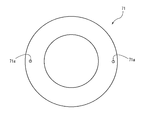
- FIG. 4 is a diagram illustrating a schematic configuration of the spacer.
- FIG. 5 is a diagram illustrating a state in which the battery unit is mounted in the electric device.
- FIG. 6 is a diagram illustrating a state in which a circuit portion is formed in an example of a battery unit manufacturing method.
- FIG. 7 is a diagram illustrating a state in which a flat battery is assembled to a circuit unit in an example of a battery unit manufacturing method.
- FIG. 8 is a diagram illustrating a schematic configuration of a spacer used in a battery unit according to a modification of the embodiment.
- FIG. 1 is a diagram showing a schematic configuration of a battery unit 1 according to an embodiment of the present invention.
- the battery unit 1 is a unit in which a coin-shaped flat battery 2 and a circuit unit 3 are integrated.
- the battery unit 1 is used as a power source for small devices using a coin-type battery, such as a pedometer, a hearing aid, an automobile electronic key, an IC tag, and a sensor unit.
- the battery unit 1 is bonded and fixed with, for example, an elastic adhesive in a state where the circuit unit 3 is laminated on the upper surface of the flat battery 2.
- the circuit unit 3 has the same shape and size as the outer shape of the flat battery 2 when viewed from the stacking direction of the flat battery 2 and the circuit unit 3.
- the flat battery 2 and the circuit unit 3 are arranged compactly in the thickness direction, and the size of the battery unit 1 is viewed from the stacking direction of the flat battery 2 and the circuit unit 3, and the outer shape of the flat battery 2.
- the shape and size can be the same.
- an elastic adhesive for bonding the flat battery 2 and the circuit unit 3 even when members having different amounts of thermal deformation are connected, the members can be bonded more reliably with the adhesive.
- various terminals 66 to 69 to be described later are formed on the surface of the circuit board 61 of the circuit unit 3 opposite to the flat battery 2. As a result, in the battery unit 1, only the various terminals 66 to 69 as shown in FIG. 2 in the state where the flat battery 2 and the circuit unit 3 are combined as shown in FIG. 67 and only the charging terminal 68 are exposed).
- the side surface of the laminate formed by fixing the flat battery 2 and the circuit portion 3 in a laminated state is a resin material that shrinks by heat, such as PET (polyethylene terephthalate). It is covered with the tube 4 (resin member) which consists of.
- the tube 4 covers not only the side surface of the laminated body but also the outer peripheral side of both end faces of the laminated body (the outer peripheral side of the substrate 61 of the circuit unit 3 and the outer peripheral side of the bottom surface of the outer can 10 of the flat battery 2).
- the external appearance of the side surface of this laminated body can also be improved.
- various terminals 66 to 69 formed on the outer surface of the circuit portion 3 located on the end face of the laminate are provided from the tube 4. Are also located inward, and the various terminals 66 to 69 are less likely to be damaged.
- the flat battery 2 includes a positive electrode can 10 as a bottomed cylindrical outer can, a negative electrode can 20 as a sealing can covering the opening of the positive electrode can 10, and an outer peripheral side of the positive electrode can 10. And the outer periphery of the negative electrode can 20, and an electrode body 40 accommodated in a space formed between the positive electrode can 10 and the negative electrode can 20. Therefore, the flat battery 2 is formed into a flat coin shape by combining the positive electrode can 10 and the negative electrode can 20 together. In the space formed between the positive electrode can 10 and the negative electrode can 20, in addition to the electrode body 40, a nonaqueous electrolytic solution (not shown) is also enclosed.
- the flat battery 2 is configured as a lithium ion battery.
- the positive electrode can 10 is made of a metal material such as stainless steel and is formed in a bottomed cylindrical shape by press molding.
- the positive electrode can 10 includes a circular bottom portion 11 and a cylindrical peripheral wall portion 12 formed continuously with the bottom portion 11 on the outer periphery thereof.
- the peripheral wall portion 12 is provided so as to extend substantially vertically from the outer peripheral end of the bottom portion 11 in a longitudinal sectional view (the state illustrated in FIG. 1).
- the positive electrode can 10 is crimped to the negative electrode can 20 by bending the opening end side of the peripheral wall portion 12 inward with the gasket 30 sandwiched between the positive electrode can 20 and the negative electrode can 20. Therefore, the bottom 11 of the positive electrode can 10 constitutes the bottom surface of the flat battery 2.
- the negative electrode can 20 is made of a metal material such as stainless steel and is formed into a bottomed cylindrical shape by press molding.
- the negative electrode can 20 has a cylindrical peripheral wall portion 22 whose outer shape is smaller than that of the peripheral wall portion 12 of the positive electrode can 10 and a circular flat portion 21 that closes one of the openings. Therefore, the flat part 21 of the negative electrode can 20 constitutes the upper surface of the flat battery 2.
- the peripheral wall portion 22 of the negative electrode can 20 is also provided so as to extend substantially perpendicular to the flat surface portion 21 in the longitudinal sectional view, similarly to the positive electrode can 10.
- the peripheral wall portion 22 is formed with an enlarged diameter portion 22b whose diameter is increased stepwise compared to the base end portion 22a on the flat surface portion 21 side. That is, the peripheral wall portion 22 is formed with a step portion 22c between the base end portion 22a and the enlarged diameter portion 22b.
- the open end side of the peripheral wall portion 12 of the positive electrode can 10 is bent and caulked with respect to the step portion 22c. That is, the positive electrode can 10 has the opening end side of the peripheral wall portion 12 fitted to the step portion 22 c of the negative electrode can 20.
- the circuit unit 3 includes a circuit board 61 and a plurality of circuit components 62 mounted on the circuit board 61.
- the plurality of circuit components 62 are mounted together on one side of the circuit board 61.
- Examples of the circuit component 62 include a protection IC that forms a protection circuit, a charging IC that forms a charging circuit, and a DC / DC converter that performs voltage conversion.
- the battery unit is matched to the rated voltage of the electric device. 1 can output a voltage. Therefore, the battery unit 1 can be configured using flat batteries having various rated voltages.
- the circuit unit 3 is configured to change the output voltage when the remaining capacity of the flat battery 2 decreases in order to detect the remaining capacity of the flat battery 2. .
- the circuit board 61 is formed to have the same shape (circular shape) and size as the outer shape of the flat battery 2 in plan view. Thereby, the circuit board 61 can prevent the battery unit 1 from becoming larger than the diameter of the flat battery 2.
- the circuit board 61 is formed in a flat plate shape, but is not limited thereto, and may be formed integrally with a spacer 71 described later.
- a GND terminal 66 (negative terminal), an output terminal 67 (positive terminal), a charging terminal 68 (positive terminal), and a charging display signal terminal 69 are provided on the surface of the circuit board 61 where the circuit component 62 is not mounted. (See FIG. 2). That is, as shown in FIG. 1, a plurality of circuit components 62 are mounted on one side of the circuit board 61, while various terminals 66 to 69 are collectively provided on the other side.
- the circuit board 61 has a plurality of through holes, and a circuit component 62 and various terminals 66 to 69 mounted on the circuit board 61 are formed by a metal material filled in the through holes. Electrically connected.
- the distance between the output terminal 67 and the adjacent terminal is such that the output terminal 67 and the charging terminal 68 can be easily distinguished. It is larger than the distance between the charging terminal 68 and the adjacent terminal (charging display signal terminal 69).
- connection terminal 63 connected to the negative electrode can 20 (negative electrode side) of the flat battery 2 and the flat battery
- a connection pin 64 connected to the second positive electrode can 10 (positive electrode side) is provided on the surface of the circuit board 61 on which the circuit component 62 is mounted.
- the connection terminal 63 and the connection pin 64 are configured to electrically connect the flat battery 2 and the circuit component 62 on the circuit board 61.
- the various terminals 66 to 69 formed on the circuit board 61 are also electrically connected to the flat battery 2 via the connection terminals 63 and the connection pins 64.
- connection terminal 63 is a member made of a conductive metal material such as copper, for example.
- the connection terminal 63 serves not only as a connection member for electrically connecting the flat battery 2 and the circuit board 61 as described above but also as a flat member. It also serves as a spacer between the battery 2 and the circuit board 61. That is, the connection terminal 63 is formed so as to have a height higher than that of the circuit component 62, so that the circuit board 61 and the flat battery 2 are sandwiched between the circuit board 61 and the flat battery 2. It is electrically connected to the flat battery 2. In this embodiment, the connection terminal 63 is also used as a spacer. However, a spacer may be provided separately from the connection terminal 63.
- connection pin 64 is a member made of a conductive metal material such as copper, and is formed in an elongated pin shape. In this embodiment, as shown in FIG. 1, two connection pins 64 are provided at positions facing each other across the flat battery 2. In this way, by providing a plurality of connection pins 64, the circuit board 61 and the flat battery 2 can be electrically connected more reliably.
- the number of connection pins 64 to be provided may be one or three or more.
- the circuit board 61 is held on the negative electrode can 20 of the flat battery 2 via a spacer 71. Specifically, the circuit board 61 is bonded and fixed to the negative electrode can 20 by an elastic adhesive in a state where the circuit board 61 is arranged at a predetermined distance from the negative electrode can 20 of the flat battery 2 by the spacer 71. Yes. Therefore, the elastic adhesive is filled between the circuit board 61 and the negative electrode can 20 of the flat battery 2. In this way, by providing the circuit board 61 on the negative electrode can 20 that is unlikely to be deformed in the flat battery 2, even if the flat battery 2 is deformed, the electrical connection between the circuit board 61 and the flat battery 2 is achieved. Secure connection.
- the spacer 71 is a member made of a resin material such as ABS resin (acrylonitrile, butadiene, styrene copolymer synthetic resin) or phenol resin, and has a substantially donut shape as shown in FIG. As shown in FIG. 1, the spacer 71 has a thick outer peripheral portion along the step portion so as to fill the step portion between the negative electrode can 20 and the positive electrode can 10 of the flat battery 2. That is, the spacer 71 is formed so that the outer peripheral side portion extends to a caulking portion (hereinafter also referred to as a shoulder portion) of the positive electrode can 10 with the negative electrode can 20.
- ABS resin acrylonitrile, butadiene, styrene copolymer synthetic resin
- phenol resin phenol resin
- the spacer 71 has a thickness such that a predetermined interval is formed between the flat battery 2 and the circuit board 61 so that the circuit component 62 does not contact the flat battery 2. Thereby, even if the flat battery 2 is deformed, the circuit component 62 can be prevented from coming into contact with the flat battery 2, and the circuit component 62 can be prevented from being damaged.
- the circuit board 61 is overlaid on the spacer 71 so that the circuit component 62 is positioned inside the substantially donut-shaped spacer 71 (see FIG. 1). Thereby, the circuit board 61 on which the circuit component 62 is mounted can be arranged compactly with respect to the flat battery 2. Moreover, since the circuit component 62 is not exposed to the outside of the battery unit 1 by adopting the configuration as described above, it is possible to prevent the user or the like from touching the circuit component 62.
- the elastic adhesive is filled between the circuit board 61 and the negative electrode can 20 of the flat battery 2, the circuit component 62 disposed on the inner side of the substantially donut-shaped spacer 71.
- the surrounding area is also filled with an elastic adhesive.
- a through hole 71a through which the connecting pin 64 is inserted is formed on the outer peripheral side of the spacer 71. As shown in FIG. 1, the through hole 71 a is formed in the thick outer peripheral portion of the spacer 71. Thereby, the connection pin 64 inserted through the through hole 71 a comes into contact with the shoulder portion of the positive electrode can 10 that is caulked to the negative electrode can 20 in the flat battery 2.
- FIG. 5 shows a state in which the battery unit 1 having the above-described configuration is arranged in a small electric device 100 such as a pedometer or a hearing aid.
- An opening 101a is formed in the housing 101 of the electric device 100 so that the GND terminal 66 and the charging terminal 68 of the battery unit 1 are exposed.
- the battery unit 1 can be charged in a state where the battery unit 1 is mounted in the housing 101 of the electric device 100. Therefore, when charging the battery unit 1, it is not necessary to remove the battery unit 1 from the electric device 100, so that time and effort during charging can be reduced.
- connection terminals 63 and connection pins 64 are provided.
- various terminals 66 to 69 are formed on the other surface side of the circuit board 61.
- the circuit board 61 is arranged so that the one surface side is on the upper side, and a spacer 71 is bonded and fixed to the circuit board 61 with an elastic adhesive.
- an elastic adhesive or the like is applied on the circuit board 61 and the spacer 71 (not shown), and as shown in FIG. 7, the flat battery 2 is placed in the circuit board 61 with the negative electrode can 20 positioned on the lower side. And on the spacer 71. Then, the elastic adhesive is dried to integrate the flat battery 2, the spacer 71 and the circuit board 61. In addition, when applying an elastic adhesive to the circuit board 61 and the spacer 71, it is necessary to be careful that the elastic adhesive does not adhere to the distal ends of the connection terminals 63 and the connection pins 64. Further, the elastic adhesive is not applied to the spacer 71 positioned on the shoulder portion of the positive electrode can 10. By doing so, it is possible to prevent the deformation of the caulking portion due to the pressure increase inside the flat battery 2 from being inhibited.
- this tube 4 is fitted on the side surface of the laminate of the flat battery 2 and the circuit portion 3 formed as described above, and the tube 4 is contracted by heating.
- this tube 4 has such a length that it covers a part of the outer peripheral side of both end faces of the laminated body in a state of being fitted to the side surface of the laminated body.
- the battery unit 1 is configured by attaching and integrating the circuit portion 3 to the flat battery 2.
- the various terminals 66 to 69 are collectively provided on the surface opposite to the flat battery 2 in the circuit board 61 of the circuit unit 3, so that the various terminals 66 to 69 are arranged at positions overlapping the flat battery 2 in plan view. 69 can be provided, and the battery unit 1 can be downsized.
- the circuit components 62 together on the surface of the flat battery 2 on the circuit board 61, it is possible to prevent the circuit components 62 and the like from being exposed to the outside of the battery unit 1. Thereby, it is possible to prevent a user touching the battery unit 1 from directly touching the circuit component 62 or the like.
- the circuit portion 3 on the negative electrode can 20 with a small deformation in the flat battery 2, the electrical connection between the flat battery 2 and the circuit portion 3 is cut by the deformation of the flat battery 2. Can be prevented. That is, by providing the circuit unit 3 on the negative electrode can 20, it is possible to ensure electrical connection between the circuit unit 3 and the flat battery 2 even when the flat battery 2 is deformed.
- the flat battery 2 is deformed by providing a spacer 71 so that a space is formed between the circuit board 61 and the flat battery 2 so that the circuit component 62 does not contact the flat battery 2. Even in this case, the circuit component 62 can be prevented from coming into contact with the flat battery 2.
- the strength of the laminated body can be improved and the appearance of the side surface of the laminated body can be improved.
- a step is formed on the end surface of the laminate by the tube 4, it is possible to reduce damage to the various terminals 66 to 69 on the circuit board 61 of the circuit unit 3.
- FIG. 8 shows a schematic configuration of the spacer 81 used in the battery unit according to the modification of the above-described embodiment.
- the configuration other than the configuration of the spacer 81 has the same configuration as that of the above-described embodiment. Therefore, the same parts as those of the embodiment are denoted by the same reference numerals and description thereof is omitted.
- the spacer 81 has a circular outer rib 81a and an inner rib 81b provided in a cross shape in the outer rib 81a.
- the outer rib 81a and the inner rib 81b are integrally formed.
- the circuit component 62 is mounted on the circuit board 61 so as to be located in the outer rib 81a of the spacer 81 and to avoid the inner rib 81b in a state where the circuit board 61 is combined with the spacer 81 described above. Is done.
- the rigidity of the spacer 81 can be increased, and the distance between the circuit board 61 and the flat battery 2 can be more reliably ensured by the spacer 81.
- the number of the inner ribs 81b of the spacer 81 may be one to three, or may be five or more.
- the spacers 71 and 81 are used to provide a gap between the circuit board 61 and the flat battery 2.
- the spacing may be formed by an adhesive without providing the spacers 71 and 81. In this case, at the time of forming the battery unit, at least one may be held so that a gap is generated between the circuit unit 3 and the flat battery 2.
- the circular spacers 71 and 81 are used.
- the present invention is not limited to this, and any spacer can be used as long as it functions as a spacer that forms a gap between the circuit board 61 and the flat battery 2. It may be a shape.
- the side surface of the laminate of the circuit unit 3 and the flat battery 2 is covered with the tube 4, but this is not a limitation, and the tube 4 may not be covered. By doing so, the battery unit can be reduced in size by not providing the tube 4. Further, instead of using the tube as in the embodiment, the side surface of the laminate may be coated with a resin material.
- the circuit board 61 has the same shape and size as the outer shape of the flat battery 2, but is not limited thereto, and the circuit board 61 may be smaller or larger than the flat battery 2. Also good. Further, the circuit board 61 may have a shape other than a circle.
- a predetermined interval is provided between the circuit component 62 of the circuit unit 3 and the flat battery 2, but this is not a limitation, and no interval may be provided.
- the circuit unit 3 may be disposed not on the negative electrode can 20 side which is a sealing can of the flat battery 2 but on the positive electrode can 10 side which is an outer can.
- the flat battery 2 and the circuit unit 3 are bonded and fixed with an elastic adhesive.
- the present invention is not limited to this, and the both may be fixed using another bonding member such as a conductive tape. .
- the outer can is the positive electrode can 10 and the sealed can is the negative electrode can 20.
- the present invention is not limited to this, and the outer can may be the negative electrode can and the sealed can may be the positive electrode can.
- the flat battery 2 is configured as a lithium ion battery.
- the flat battery 2 may be a battery other than a lithium ion battery as long as it is a rechargeable secondary battery.
- the flat battery 2 may be a primary battery.
- a capacitor or the like is mounted as a circuit unit.
- the battery unit according to the present invention can be used in a configuration including a substrate on which a circuit is formed and a flat battery attached to a small device.
Landscapes
- Chemical & Material Sciences (AREA)
- Chemical Kinetics & Catalysis (AREA)
- Electrochemistry (AREA)
- General Chemical & Material Sciences (AREA)
- Engineering & Computer Science (AREA)
- Microelectronics & Electronic Packaging (AREA)
- Manufacturing & Machinery (AREA)
- Battery Mounting, Suspending (AREA)
- Connection Of Batteries Or Terminals (AREA)
- Sealing Battery Cases Or Jackets (AREA)
Abstract
Priority Applications (6)
| Application Number | Priority Date | Filing Date | Title |
|---|---|---|---|
| JP2013500779A JP5697275B2 (ja) | 2011-02-23 | 2011-02-23 | 電池ユニット及び電気機器 |
| US14/000,325 US8822049B2 (en) | 2011-02-23 | 2011-02-23 | Battery unit and electrical device |
| KR1020137023990A KR101351428B1 (ko) | 2011-02-23 | 2011-02-23 | 전지 유닛 및 전기 기기 |
| PCT/JP2011/054049 WO2012114489A1 (fr) | 2011-02-23 | 2011-02-23 | Unité de batterie, et dispositif électrique |
| EP11859623.8A EP2680338B1 (fr) | 2011-02-23 | 2011-02-23 | Unité de batterie, et dispositif électrique |
| CN201180067995.8A CN103384927B (zh) | 2011-02-23 | 2011-02-23 | 电池单元及电气设备 |
Applications Claiming Priority (1)
| Application Number | Priority Date | Filing Date | Title |
|---|---|---|---|
| PCT/JP2011/054049 WO2012114489A1 (fr) | 2011-02-23 | 2011-02-23 | Unité de batterie, et dispositif électrique |
Publications (1)
| Publication Number | Publication Date |
|---|---|
| WO2012114489A1 true WO2012114489A1 (fr) | 2012-08-30 |
Family
ID=46720307
Family Applications (1)
| Application Number | Title | Priority Date | Filing Date |
|---|---|---|---|
| PCT/JP2011/054049 Ceased WO2012114489A1 (fr) | 2011-02-23 | 2011-02-23 | Unité de batterie, et dispositif électrique |
Country Status (6)
| Country | Link |
|---|---|
| US (1) | US8822049B2 (fr) |
| EP (1) | EP2680338B1 (fr) |
| JP (1) | JP5697275B2 (fr) |
| KR (1) | KR101351428B1 (fr) |
| CN (1) | CN103384927B (fr) |
| WO (1) | WO2012114489A1 (fr) |
Cited By (3)
| Publication number | Priority date | Publication date | Assignee | Title |
|---|---|---|---|---|
| JP2013025950A (ja) * | 2011-07-19 | 2013-02-04 | Hitachi Maxell Energy Ltd | 電池ユニット |
| JP2013025951A (ja) * | 2011-07-19 | 2013-02-04 | Hitachi Maxell Energy Ltd | 電池ユニット |
| WO2014010396A1 (fr) * | 2012-07-13 | 2014-01-16 | 日立マクセル株式会社 | Unité de pile |
Families Citing this family (6)
| Publication number | Priority date | Publication date | Assignee | Title |
|---|---|---|---|---|
| WO2012147375A1 (fr) * | 2011-04-27 | 2012-11-01 | 日立マクセルエナジー株式会社 | Unité batterie |
| WO2013105231A1 (fr) | 2012-01-11 | 2013-07-18 | 日立マクセル株式会社 | Unité de batterie |
| EP3357103B1 (fr) | 2015-09-30 | 2021-11-17 | Fossil Group, Inc. | Systèmes, dispositifs et procédés d'utilisation d'un boîtier conducteur pour un contact de pile |
| KR102068708B1 (ko) * | 2015-11-23 | 2020-01-22 | 주식회사 엘지화학 | 2차 전지 |
| US10698445B1 (en) * | 2018-12-14 | 2020-06-30 | Dell Products L.P. | Information handling system multi-cell cantilevered battery |
| CN114006090A (zh) * | 2020-07-28 | 2022-02-01 | 曙鹏科技(深圳)有限公司 | 纽扣电池 |
Citations (5)
| Publication number | Priority date | Publication date | Assignee | Title |
|---|---|---|---|---|
| JPH0584147U (ja) * | 1992-04-14 | 1993-11-12 | 三洋電機株式会社 | コイン形電池を有する電池ユニット |
| JP2009087554A (ja) * | 2007-09-27 | 2009-04-23 | Hitachi Maxell Ltd | 電池パック |
| JP2009152183A (ja) | 2007-11-26 | 2009-07-09 | Hitachi Maxell Ltd | 密閉型電池、及びこの密閉型電池を用いた電池パックと、この電池パックを搭載した電子機器 |
| JP3159789U (ja) * | 2010-03-15 | 2010-06-03 | Kfe Japan株式会社 | コイン形電池用電池ケース |
| JP2010205700A (ja) * | 2009-03-06 | 2010-09-16 | Hitachi Maxell Ltd | 電池ユニット |
Family Cites Families (12)
| Publication number | Priority date | Publication date | Assignee | Title |
|---|---|---|---|---|
| JPH0423711U (fr) * | 1990-06-18 | 1992-02-26 | ||
| US5993248A (en) * | 1997-11-20 | 1999-11-30 | Itt Manufacturing Enterprises, Inc. | Battery connector |
| US6109530A (en) * | 1998-07-08 | 2000-08-29 | Motorola, Inc. | Integrated circuit carrier package with battery coin cell |
| WO2001073883A2 (fr) * | 2000-03-24 | 2001-10-04 | Cymbet Corporation | Fabrication basse temperature de dispositifs d'accumulation d'energie en couche mince |
| JP3625778B2 (ja) | 2001-03-30 | 2005-03-02 | 三洋電機株式会社 | コイン型電気素子を実装するプリント基板 |
| KR100861166B1 (ko) * | 2002-02-13 | 2008-09-30 | 마츠시타 덴끼 산교 가부시키가이샤 | 전지 팩의 제조방법 |
| US7603144B2 (en) * | 2003-01-02 | 2009-10-13 | Cymbet Corporation | Active wireless tagging system on peel and stick substrate |
| JP3696217B2 (ja) * | 2003-03-11 | 2005-09-14 | ムネカタ株式会社 | 電子部品の低圧、低温絶縁被覆方法 |
| JP4009563B2 (ja) * | 2003-06-27 | 2007-11-14 | ムネカタ株式会社 | コンタクト付電池 |
| WO2007080820A1 (fr) * | 2006-01-12 | 2007-07-19 | Kabushiki Kaisha Toshiba | Recepteur de puissance, appareil electronique l'utilisant et chargeur sans contact |
| JP4855104B2 (ja) * | 2006-03-03 | 2012-01-18 | 三洋電機株式会社 | 電池パック |
| JP2007257849A (ja) * | 2006-03-20 | 2007-10-04 | Hitachi Maxell Ltd | ラミネート外装扁平形電池の電池モジュール |
-
2011
- 2011-02-23 KR KR1020137023990A patent/KR101351428B1/ko active Active
- 2011-02-23 EP EP11859623.8A patent/EP2680338B1/fr active Active
- 2011-02-23 WO PCT/JP2011/054049 patent/WO2012114489A1/fr not_active Ceased
- 2011-02-23 CN CN201180067995.8A patent/CN103384927B/zh active Active
- 2011-02-23 US US14/000,325 patent/US8822049B2/en active Active
- 2011-02-23 JP JP2013500779A patent/JP5697275B2/ja active Active
Patent Citations (5)
| Publication number | Priority date | Publication date | Assignee | Title |
|---|---|---|---|---|
| JPH0584147U (ja) * | 1992-04-14 | 1993-11-12 | 三洋電機株式会社 | コイン形電池を有する電池ユニット |
| JP2009087554A (ja) * | 2007-09-27 | 2009-04-23 | Hitachi Maxell Ltd | 電池パック |
| JP2009152183A (ja) | 2007-11-26 | 2009-07-09 | Hitachi Maxell Ltd | 密閉型電池、及びこの密閉型電池を用いた電池パックと、この電池パックを搭載した電子機器 |
| JP2010205700A (ja) * | 2009-03-06 | 2010-09-16 | Hitachi Maxell Ltd | 電池ユニット |
| JP3159789U (ja) * | 2010-03-15 | 2010-06-03 | Kfe Japan株式会社 | コイン形電池用電池ケース |
Non-Patent Citations (1)
| Title |
|---|
| See also references of EP2680338A4 |
Cited By (3)
| Publication number | Priority date | Publication date | Assignee | Title |
|---|---|---|---|---|
| JP2013025950A (ja) * | 2011-07-19 | 2013-02-04 | Hitachi Maxell Energy Ltd | 電池ユニット |
| JP2013025951A (ja) * | 2011-07-19 | 2013-02-04 | Hitachi Maxell Energy Ltd | 電池ユニット |
| WO2014010396A1 (fr) * | 2012-07-13 | 2014-01-16 | 日立マクセル株式会社 | Unité de pile |
Also Published As
| Publication number | Publication date |
|---|---|
| KR20130109253A (ko) | 2013-10-07 |
| EP2680338A1 (fr) | 2014-01-01 |
| CN103384927B (zh) | 2015-08-19 |
| US20130323538A1 (en) | 2013-12-05 |
| JPWO2012114489A1 (ja) | 2014-07-07 |
| EP2680338A4 (fr) | 2014-08-27 |
| EP2680338B1 (fr) | 2015-09-09 |
| US8822049B2 (en) | 2014-09-02 |
| CN103384927A (zh) | 2013-11-06 |
| JP5697275B2 (ja) | 2015-04-08 |
| KR101351428B1 (ko) | 2014-01-14 |
Similar Documents
| Publication | Publication Date | Title |
|---|---|---|
| JP5697275B2 (ja) | 電池ユニット及び電気機器 | |
| JP5652976B2 (ja) | 電池ユニット | |
| WO2014010396A1 (fr) | Unité de pile | |
| JP5878564B2 (ja) | 電池ユニット | |
| JP5996302B2 (ja) | 電池ユニット | |
| JP5530382B2 (ja) | 電池ユニット及び該電池ユニットと電気機器との接続端子構造 | |
| JP5670271B2 (ja) | 電池ユニット | |
| JP5822730B2 (ja) | 電池ユニット | |
| JP5670270B2 (ja) | 電池ユニット | |
| JP5885508B2 (ja) | 電池ユニット | |
| JP5822731B2 (ja) | 電池ユニット | |
| US9257688B2 (en) | Battery pack having an inner frame and an outer frame | |
| JP5530381B2 (ja) | 電池ユニット | |
| KR20140098480A (ko) | 이차전지 |
Legal Events
| Date | Code | Title | Description |
|---|---|---|---|
| 121 | Ep: the epo has been informed by wipo that ep was designated in this application |
Ref document number: 11859623 Country of ref document: EP Kind code of ref document: A1 |
|
| ENP | Entry into the national phase |
Ref document number: 2013500779 Country of ref document: JP Kind code of ref document: A |
|
| WWE | Wipo information: entry into national phase |
Ref document number: 14000325 Country of ref document: US |
|
| WWE | Wipo information: entry into national phase |
Ref document number: 2011859623 Country of ref document: EP |
|
| NENP | Non-entry into the national phase |
Ref country code: DE |
|
| ENP | Entry into the national phase |
Ref document number: 20137023990 Country of ref document: KR Kind code of ref document: A |