WO2012114525A1 - Dispositif de commande, système de commande et procédé de communication - Google Patents
Dispositif de commande, système de commande et procédé de communication Download PDFInfo
- Publication number
- WO2012114525A1 WO2012114525A1 PCT/JP2011/054394 JP2011054394W WO2012114525A1 WO 2012114525 A1 WO2012114525 A1 WO 2012114525A1 JP 2011054394 W JP2011054394 W JP 2011054394W WO 2012114525 A1 WO2012114525 A1 WO 2012114525A1
- Authority
- WO
- WIPO (PCT)
- Prior art keywords
- data
- information
- memory
- storage
- control device
- Prior art date
- Legal status (The legal status is an assumption and is not a legal conclusion. Google has not performed a legal analysis and makes no representation as to the accuracy of the status listed.)
- Ceased
Links
Images







Classifications
-
- G—PHYSICS
- G06—COMPUTING OR CALCULATING; COUNTING
- G06F—ELECTRIC DIGITAL DATA PROCESSING
- G06F13/00—Interconnection of, or transfer of information or other signals between, memories, input/output devices or central processing units
- G06F13/14—Handling requests for interconnection or transfer
-
- H—ELECTRICITY
- H04—ELECTRIC COMMUNICATION TECHNIQUE
- H04L—TRANSMISSION OF DIGITAL INFORMATION, e.g. TELEGRAPHIC COMMUNICATION
- H04L67/00—Network arrangements or protocols for supporting network services or applications
- H04L67/01—Protocols
- H04L67/12—Protocols specially adapted for proprietary or special-purpose networking environments, e.g. medical networks, sensor networks, networks in vehicles or remote metering networks
-
- G—PHYSICS
- G06—COMPUTING OR CALCULATING; COUNTING
- G06F—ELECTRIC DIGITAL DATA PROCESSING
- G06F11/00—Error detection; Error correction; Monitoring
- G06F11/07—Responding to the occurrence of a fault, e.g. fault tolerance
- G06F11/08—Error detection or correction by redundancy in data representation, e.g. by using checking codes
- G06F11/10—Adding special bits or symbols to the coded information, e.g. parity check, casting out 9's or 11's
-
- G—PHYSICS
- G06—COMPUTING OR CALCULATING; COUNTING
- G06F—ELECTRIC DIGITAL DATA PROCESSING
- G06F12/00—Accessing, addressing or allocating within memory systems or architectures
-
- G—PHYSICS
- G06—COMPUTING OR CALCULATING; COUNTING
- G06F—ELECTRIC DIGITAL DATA PROCESSING
- G06F12/00—Accessing, addressing or allocating within memory systems or architectures
- G06F12/02—Addressing or allocation; Relocation
-
- G—PHYSICS
- G06—COMPUTING OR CALCULATING; COUNTING
- G06F—ELECTRIC DIGITAL DATA PROCESSING
- G06F12/00—Accessing, addressing or allocating within memory systems or architectures
- G06F12/02—Addressing or allocation; Relocation
- G06F12/0223—User address space allocation, e.g. contiguous or non contiguous base addressing
- G06F12/0292—User address space allocation, e.g. contiguous or non contiguous base addressing using tables or multilevel address translation means
-
- G—PHYSICS
- G06—COMPUTING OR CALCULATING; COUNTING
- G06F—ELECTRIC DIGITAL DATA PROCESSING
- G06F13/00—Interconnection of, or transfer of information or other signals between, memories, input/output devices or central processing units
- G06F13/38—Information transfer, e.g. on bus
-
- G—PHYSICS
- G05—CONTROLLING; REGULATING
- G05B—CONTROL OR REGULATING SYSTEMS IN GENERAL; FUNCTIONAL ELEMENTS OF SUCH SYSTEMS; MONITORING OR TESTING ARRANGEMENTS FOR SUCH SYSTEMS OR ELEMENTS
- G05B19/00—Program-control systems
- G05B19/43—Program-control systems fluidic
- G05B19/44—Program-control systems fluidic pneumatic
-
- G—PHYSICS
- G06—COMPUTING OR CALCULATING; COUNTING
- G06F—ELECTRIC DIGITAL DATA PROCESSING
- G06F2213/00—Indexing scheme relating to interconnection of, or transfer of information or other signals between, memories, input/output devices or central processing units
- G06F2213/0038—System on Chip
-
- H—ELECTRICITY
- H04—ELECTRIC COMMUNICATION TECHNIQUE
- H04L—TRANSMISSION OF DIGITAL INFORMATION, e.g. TELEGRAPHIC COMMUNICATION
- H04L1/00—Arrangements for detecting or preventing errors in the information received
- H04L1/004—Arrangements for detecting or preventing errors in the information received by using forward error control
- H04L1/0056—Systems characterized by the type of code used
- H04L1/0061—Error detection codes
Definitions
- the present invention relates to a control device, a control system, and a communication method.
- control device composed of a controller that controls the entire device and a plurality of motors
- the controller and the plurality of motors are generally connected by serial communication.
- serial communication By connecting each device by serial communication, it is possible to realize wiring saving and improvement in maintainability of the entire device.
- the plurality of motors are generally composed of a motor and a motor driving device, and serial communication is performed between the controller and the motor driving device.
- serial communication movement commands such as position, speed, and torque are transmitted from the controller to the motor drive device, and control state quantities such as the motor position, speed, and drive current value are transmitted from the motor drive device.
- serial communication for drive control for the purpose of motor control
- movement commands and control state quantities are transmitted to each other at regular intervals in order to stably operate the motor.
- Serial communication control The movement command is sequentially updated and transmitted from the controller to the motor drive device at a constant communication cycle, and the motor drive device performs reception processing at each communication cycle and performs motor control so as to follow the command extracted from the received data. By doing so, the controller can control the motor at a desired position, speed, torque, and the like.
- the controller receives the control state quantity that is sequentially updated and transmitted from the motor drive device at a constant communication cycle for each communication cycle, and drives the motor from the necessary control state quantity extracted from the received data. Control processing necessary for the apparatus is performed, and the entire motor driving apparatus is controlled by reflecting it in the next motor control command.
- the reception control unit of serial communication updates the reception data for each communication cycle.
- a FIFO (First In, First Out) buffer as a buffer memory for storing received data, multiple received data can be held in one communication cycle, or multiple received data can be held in multiple communication cycles To do.
- the reception control unit In the case where the reception control unit holds a plurality of received data in a plurality of communication cycles, in the serial communication for drive control, once communication between devices is started, a specified communication frame is periodically transmitted in a specified communication cycle. Is done. Therefore, the reception control unit periodically stores the reception data of each communication frame in the reception buffer memory according to a management table that manages the storage position of the reception data (see, for example, Patent Document 1).
- inspection data for detecting data corruption on the communication path is attached to the communication frame at the time of transmission, and the reliability of the received data from the received data and the inspection data on the receiving side Is confirmed and held as the received data state.
- it is necessary to hold the received data state as much as the received data that is held see, for example, Patent Document 2.
- the above-mentioned serial communication frame is transmitted with a specific bit pattern added to the beginning and end of the data to be transmitted.
- the start specific bit pattern is the start flag
- the last bit pattern is the end flag
- the reception unit identifies the start flag to start the communication frame reception process, and the end flag recognizes the end of the communication frame.
- One communication frame is received.
- the received data is generally stored in order in the buffer memory.
- the received data is stored anywhere in the buffer memory.
- a reception data processing unit for processing which reception data should be extracted from where is required.
- the received data and the received data state are held separately, and in particular, when holding a plurality of received data, it is necessary to clarify the combination of the received data and the received data state.
- the missing communication frame is identified. There is a problem that it takes time to process the received data and the received data state.
- the present invention has been made in view of the above, and obtains a control device, a control system, and a communication method capable of simply extracting received data from a buffer memory in which a plurality of received data is stored in drive control serial communication. With the goal.
- the transmitting unit stores data to be transmitted to another control device Transmission control means for generating a frame including a memory, the data acquired from the memory, and memory storage information indicating a storage position of the data in a buffer memory of the reception unit of the other control device.
- the reception unit includes: a reception control unit that extracts the memory storage information and the data from the frame; and a buffer that stores the extracted data.
- a memory, and data storage processing means for storing the extracted data at an address of the buffer memory specified by the memory storage information, wherein the memory storage information is for each control device serving as a destination of the frame.
- the control unit reads data from another control device every time from an address fixed for each of the other control devices of the buffer memory.
- the received data is stored at a specific address of the buffer memory according to the memory storage information in the frame, it is necessary to hold information for managing the storage position of the received data in the buffer memory on the receiving unit side And the processing time at the time of reception can be shortened.
- the processing time required for reception processing is shortened, the data update cycle between the control devices can be increased, and the performance of the entire network to which the control devices are connected can be improved. .
- FIG. 1 is a diagram schematically showing an example of a motor drive control system configured in a network by serial communication according to Embodiment 1 of the present invention.
- FIG. 2 is a diagram illustrating an example of a transmission timing of data transmitted from the controller to each motor driving device.
- FIG. 3 is a diagram illustrating an example of a transmission timing of data transmitted from each motor driving device to the controller.
- FIG. 4 is a diagram illustrating an example of transmission timing of data transmitted between the controller and each motor driving device.
- FIG. 5 is a block diagram schematically showing a functional configuration of a transmission unit provided in the unit according to the first embodiment.
- FIG. 6 is a diagram illustrating an example of a frame configuration used in the embodiment.
- FIG. 1 is a diagram schematically showing an example of a motor drive control system configured in a network by serial communication according to Embodiment 1 of the present invention.
- FIG. 2 is a diagram illustrating an example of a transmission timing of data transmitted from the controller to each motor driving device.
- FIG. 7 is a block diagram schematically showing a functional configuration of a receiving unit provided in the unit according to the first embodiment.
- FIG. 8 is a diagram schematically illustrating an example of the state of the buffer memory of the controller.
- FIG. 9 is a diagram schematically illustrating an example of a state of a buffer memory of a general reception unit.
- FIG. 10 is a diagram schematically illustrating an example of a state of a buffer memory of a general reception unit.
- FIG. 11 is a flowchart illustrating an example of a procedure of frame transmission processing according to the first embodiment.
- FIG. 12 is a flowchart illustrating an example of a frame reception process procedure according to the first embodiment.
- FIG. 13 is a block diagram schematically showing the configuration of the receiving unit according to the second embodiment.
- FIG. 14 is a diagram schematically illustrating an example of the state of the buffer memory of the controller according to the second embodiment.
- FIG. 15 is a block diagram schematically showing a configuration of a receiving unit according to the third embodiment.
- FIG. 16 is a diagram schematically illustrating an example of the configuration of the conversion table unit according to the third embodiment.
- FIG. 17 is a diagram schematically illustrating an example of a table configuration.
- FIG. 18 is a diagram schematically illustrating an example of the state of the buffer memory of the controller according to the third embodiment.
- FIG. 19 is a diagram schematically illustrating an example of the configuration of the conversion table unit according to the fourth embodiment.
- FIG. 20 is a diagram schematically illustrating an example of a table configuration.
- FIG. 21 is a diagram schematically illustrating an example of the state of the buffer memory of the controller according to the fourth embodiment.
- FIG. 1 is a diagram schematically showing an example of a motor drive control system configured in a network by serial communication according to Embodiment 1 of the present invention.
- This motor drive control system includes a plurality of motors 11-1 to 11-3 such as servo motors and induction motors to be controlled, and motor drive devices 12-1 to 12-3 for controlling the respective motors 11-1 to 11-3. 12-3 and a controller 13 for controlling the operation of the entire motor driving devices 12-1 to 12-3.
- the controller 13 and the motor driving devices 12-1 to 12-3 are connected by a serial communication line 21 to perform data communication.
- the motor driving devices 12-1 to 12-3 and the motors 11-1 to 11-3 are connected by a power line 22 and a detector cable 23, respectively.
- the motor driving devices 12-1 to 12-3 transmit motor driving power to the motors 11-1 to 11-3 through the power line 22, and the motors 11-1 to 11-3 are motors 11-1 to 11-11.
- Motor angle information acquired by a detector (not shown) that detects the rotation angle of ⁇ 3 is transmitted to the motor driving devices 12-1 to 12-3 via the detector cable 23.
- the motor driving devices 12-1 to 12-3 control the motor angle in accordance with a command from the controller 13 based on the motor driving power and the motor angle information.
- the motor angle information is used in the motor drive control.
- the motor angle information is not necessarily used in the motor drive control, and other information is used without using the motor angle information. Then, motor drive control may be performed.
- the controller 13 and the motor drive devices 12-1 to 12-3 each have a control unit, a transmission unit, and a reception unit, perform data communication via the serial communication line 21, and the controller 13 to the motor drive devices 12-1 to 12-12.
- a movement command such as position, speed, torque, and other control signals are transmitted to -3.
- the controller 13 of each of the motor drive devices 12-1 to 12-3 controls the motors 11-1 to 11-3 with the commanded position, speed, and torque by the movement command from the controller 13, so that the controller 13 drives the motor.
- the entire devices 12-1 to 12-3 can be controlled. Further, the positions, speeds, driving currents, various control signals, and abnormal states of the motors 11-1 to 11-3 are transmitted from the motor driving devices 12-1 to 12-3 to the controller 13.
- the controller of the controller 13 feeds back the control state as necessary to control the next command, or issues a stop command to the motor drive devices 12-1 to 12-3 when the motor control is determined to be abnormal. To do.
- the controller 13 constitutes a control device or an overall control device, and the motor drive devices 12-1 to 12-3 constitute a control device.
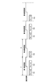
- FIG. 2 is a diagram illustrating an example of a transmission timing of data transmitted from the controller to each motor driving device. Communication at regular intervals is defined by a communication cycle T.
- the data transmitted from the controller 13 to the motor drive device 12-1 is a frame 101
- the data transmitted from the controller 13 to the motor drive devices 12-2 and 12-3 are frames 102 and 103, respectively. Shall.
- the controller 13 transmits a frame 101 including command data to the motor driving device 12-1 and a frame 102 including command data to the motor driving device 12-2 in the first communication cycle,
- the frame 103 including the command data to the motor drive device 12-3 is transmitted in the next second communication cycle.
- the controller 13 transmits a frame 101 including the next command data to the motor driving device 12-1 and a frame 102 including the next command data to the motor driving device 12-2 in the third communication cycle, and the fourth The frame 103 including the next command data to the motor driving device 12-3 is transmitted in the communication cycle.
- the command data updated at regular intervals is transmitted from the controller 13 to each of the motor driving devices 12-1 to 12-3, so that the controller 13 can perform motor control.
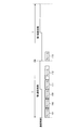
- FIG. 3 is a diagram illustrating an example of the transmission timing of data transmitted from each motor drive device to the controller. Also in this example, communication at regular intervals is defined by the communication cycle T.
- the communication cycle T may or may not be the same as the communication cycle T at the time of data transmission from the controller 13 of FIG. 2 to the motor driving devices 12-1 to 12-3.
- the data transmitted from the motor driving device 12-1 to the controller 13 is a frame 111
- the data transmitted from the motor driving device 12-2, 12-3 to the controller 13 is a frame 112, 113, respectively. .
- a frame 111 including state data is transmitted from the motor driving device 12-1, and a frame 112 including state data is transmitted from the motor driving device 12-2.
- a frame 113 including state data is transmitted from the motor driving device 12-3.
- frames 111 and 112 including the next state data are transmitted from the motor driving devices 12-1 and 12-2, respectively, and in the fourth communication cycle, the next state is transmitted from the motor driving device 12-3.
- a frame 113 including data is transmitted.
- various states of the motor drive devices 12-1 to 12-3 updated at regular intervals are transmitted to the controller 13.
- the controller 13 controls the entire system according to the state of each of the motor driving devices 12-1 to 12-3, or sequentially grasps the state of each of the motor driving devices 12-1 to 12-3. If the whole is in a dangerous state, it is possible to take measures such as stopping the motors 11-1 to 11-3.
- FIG. 4 is a diagram illustrating an example of transmission timing of data transmitted between the controller and each motor driving device.
- the fixed interval is defined by the communication cycle T, data transmitted from the controller 13 to each of the motor drive devices 12-1 to 12-3, and from each motor drive device 12-1 to 12-3 to the controller 13 It is an example of each transmission timing of the data transmitted to.
- the same frames as those in FIGS. 2 to 3 are denoted by the same reference numerals.
- frames 101 to 103 including command data are transmitted from the controller 13 to the motor drive devices 12-1 to 12-3, respectively, and the motor drive devices 12-1 and 12- Frames 111 and 112 including state data are transmitted from 2 to the controller 13, respectively.
- the frame 113 including the state data is transmitted from the motor driving device 12-3 to the controller 13.
- one command data and status data are transmitted and received in the first communication cycle and the second communication cycle, and one command data and status updated in the next third communication cycle and the fourth communication cycle. Data is sent and received. That is, the command data and the status data are updated at regular intervals as in the examples of FIGS.
- Each unit constituting such a motor drive control system has a transmission unit that transmits data to other units and a reception unit that receives data from other units.
- FIG. 5 is a block diagram schematically showing a functional configuration of a transmission unit provided in the unit according to the first embodiment.
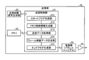
- the transmission unit 30 includes a transmission control unit 31, a transmission activation signal generation unit 32, a memory 33, a conversion unit 34, and a transmission buffer 35.
- the transmission control unit 31 starts the operation in response to the activation signal from the transmission activation signal generation unit 32, generates transmission data as a frame defined by the communication protocol, and controls the entire transmission.
- FIG. 6 is a diagram illustrating an example of a frame configuration used in the embodiment.
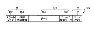
- the frame 130 has a data structure to which various flags necessary for the receiving unit to analyze serial data in addition to the data to be transmitted are added.
- the frame header part 131 includes a start flag 132 for identifying the head of the frame 130, and memory storage information 133 for storing information unique to the communication frame.
- the frame data unit 134 includes data 135 for storing data transmitted by each unit, and frame inspection data 136 such as CRC (Cyclic Redundancy Check) information and checksum information for determining whether the received frame 130 is normal data. And having.
- the frame inspection data 136 can be the inspection target from the start flag 132 of the frame header part 131 to the data 135 of the frame data part 134, but is not limited thereto.
- the frame footer unit 137 has an end flag 138 for identifying the end of the frame.
- the memory storage information 133 defines an address in the buffer memory of the receiving side control device in which the data 135 of the frame data unit 134 is stored. For example, the address stored in the buffer memory of the receiving side control device is determined for each type of the frames 101 to 103 and 111 to 113 transmitted at a constant cycle shown in FIGS. Accordingly, the memory storage information 133 stores the address in the buffer memory of the receiving side control device.
- the transmission control unit 31 includes a start flag generation unit 311, a memory storage information generation unit 312, a transmission data acquisition unit 313, a frame inspection data generation unit 314, and an end flag generation unit 315.
- the frame 130 is composed of a start flag 132, memory storage information 133, data 135, frame inspection data 136, and end flag 138 in order from the top. It is generated by the memory storage information generation unit 312, the transmission data acquisition unit 313, the frame inspection data generation unit 314, and the end flag generation unit 315.
- the start flag generation unit 311 generates a specific bit pattern specific to the communication protocol as the start flag 132.
- the memory storage information generation unit 312 generates information as to which address of the buffer memory of the unit the frame 130 received by the reception unit of the destination unit should be stored as memory storage information 133 for each frame. At the time of generation, for example, reference is made to frame-reception destination buffer address association information (not shown) that associates the destination unit with the address in the buffer memory of the receiving unit that stores the data 135.
- the transmission data acquisition unit 313 reads data to be transmitted from the memory 33 and sets it as data 135.
- the frame inspection data generation unit 314 calculates CRC information and checksum information of the frame data and adds them as frame inspection data 136.
- the end flag generation unit 315 generates a specific bit pattern specific to the communication protocol as the end flag 138 in the same manner as the start flag 132.
- the transmission activation signal generation unit 32 generates a transmission activation signal for the transmission control unit 31 in accordance with a predetermined transmission timing in order to output transmission data having a fixed period. As a result, transmission data updated at regular intervals with regular communication cycles as shown in FIGS. 2 to 4 is transmitted.
- the memory 33 stores data to be transmitted to other units constituting the motor drive control system.
- the data stored in the memory 33 is periodically rewritten by the CPU or the like, and the transmission data is sequentially updated.
- the conversion unit 34 converts parallel data output by the transmission control unit 31 as transmission data into serial data.
- the transmission buffer 35 transmits serial data.
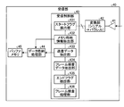
- FIG. 7 is a block diagram schematically showing a functional configuration of a receiving unit provided in the unit according to the first embodiment.
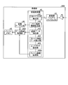
- the reception unit 40 includes a reception buffer 41, a conversion unit 42, a reception control unit 43, a data storage processing unit 44, and a buffer memory 45.
- the reception buffer 41 receives a serial data frame.
- the converter 42 sequentially converts the received serial data into parallel data.
- the reception control unit 43 is a processing unit that analyzes the received frame 130, and includes a start flag detection unit 431, a memory storage information extraction unit 432, a transmission data extraction unit 433, a frame inspection data extraction unit 434, an end flag extraction unit 435, and A frame inspection processing unit 436 is included.
- the reception control unit 43 sequentially detects the start flag 132 which is the head of the frame 130 converted into parallel data by the conversion unit 42, and information on the frame 130 specified by the communication protocol from the time when the start flag 132 is detected.
- the start flag 132, the memory storage information 133, the data 135, the frame inspection data 136, and the end flag 138 are extracted from the frame 130.
- the start flag detection unit 431 sequentially compares the parallel data output from the conversion unit 42 with a start flag pattern, and performs coincidence detection. Then, when it coincides with the start flag pattern, a start flag detection signal is output, and the memory storage information extraction unit 432 is activated.
- the memory storage information extraction unit 432 uses the fact that the start flag 132 and the memory storage information 133 are normally specified as data of a certain length, and stores data of a specified length from the time when the start flag 132 is detected. Extracted as stored information 133. When the extraction of the memory storage information 133 is completed, a completion signal indicating completion of extraction of the memory storage information 133 is output to the transmission data extraction unit 433.
- the transmission data extraction unit 433 receives the completion signal from the memory storage information extraction unit 432 and starts extracting the data 135. In the extraction of the data 135, the head of the data 135 starts from the next of the memory storage information 133. However, since the length of the data 135 differs depending on the frame 130, it is difficult to extract the data 135. Incidentally, the frame inspection data 136 and the end flag 138 arranged after the data 135 are defined as data having a predetermined length by the communication protocol. Therefore, the transmission data extraction unit 433 uses this to identify the end of the data 135 by going back the length of the end flag 138 and the frame inspection data 136 from the time when the end flag 138 is identified. That is, the data 135 in the frame 130 is extracted by identifying the beginning and end of the data 135. When the extraction of the data 135 is completed, a completion signal indicating the data extraction is output to the frame inspection data extraction unit 434.
- the frame inspection data extraction unit 434 extracts the frame inspection data 136 from the frame 130 in response to the completion signal from the transmission data extraction unit 433. Since the frame inspection data 136 is arranged next to the data 135, the frame inspection data 136 is extracted by going back the length of the end flag 138 when the end flag 138 is identified, as in the last identification of the data 135. To do.
- the end flag extraction unit 435 identifies the end of the frame 130 when the parallel data output from the conversion unit 42 matches the end flag pattern, and activates the frame inspection processing unit 436.
- the frame inspection processing unit 436 performs frame inspection calculation such as CRC or checksum of the received frame 130 and compares it with the frame inspection data 136 extracted from the frame 130 to determine whether the received frame 130 is normal. Is determined.
- the data storage processing unit 44 stores the extracted data 135 as reception data in the buffer memory 45 based on the memory storage information 133 extracted by the reception control unit 43.
- the buffer memory 45 stores the received data.
- the data storage position in the buffer memory 45 is determined by the transmission source unit.
- the data 135 is stored at the address specified by the memory storage information 133.
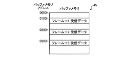
- FIG. 8 is a diagram schematically showing an example of the state of the buffer memory of the controller.
- data extracted from the frames 111 to 113 received from the motor drive devices 12-1 to 12-3 are stored at addresses “0100h”, “0200h”, and “0300h” of the buffer memory 45.
- Addresses for storing data in the frames 111 to 113 are determined from the memory storage information extracted from the frames 111 to 113, respectively.
- “0100h” is set as the address of the buffer memory 45 of the receiving unit that stores data in the memory storage information of the frame 111 transmitted by the motor driving device 12-1.
- the memory storage information of the frames 112 and 113 transmitted by the motor driving devices 12-2 and 12-3 includes “0200h” and “0300h” as addresses of the buffer memory 45 of the receiving unit that stores the data, respectively. Is set.
- the controller 13 manages the address of the buffer memory 45 in association with the motor driving devices 12-1 to 12-3 that transmitted the data stored at the address. At this time, the address of the buffer memory 45 is fixed to the motor driving devices 12-1 to 12-3. Therefore, each time the data is updated, the controller 13 receives data corresponding to each motor driving device 12-1 to 12-3 from the address fixed for each motor driving device 12-1 to 12-3 in the buffer memory 45. Is read out, the state data such as the motor position, motor speed, drive current, various control signals, and abnormal state of each of the motor drive devices 12-1 to 12-3 can be acquired.
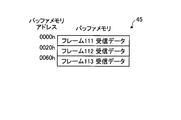
- FIG. 9 and FIG. 10 are diagrams schematically showing an example of a state of a buffer memory of a general receiving unit.
- FIG. 9 shows a state of a buffer memory of a general receiving unit when a frame is normally received.
- FIG. 10 is a diagram schematically illustrating an example of a state of a buffer memory of a general reception unit when a frame cannot be normally received. Again, the buffer state of the controller 13 of the motor drive control system shown in FIG. 1 is shown.
- the receiving unit of a general unit arranges received data in the order received from the top (first address) of the buffer memory 45.
- the arrangement of the data stored in the buffer memory 45 changes as shown in FIG. FIG. 10 shows the state of the buffer memory 45 when the frame 112 that should be received for the second time is not received.
- the controller 13 when the controller 13 reads data from the buffer memory 45 and receives it normally as shown in FIG. 9, there is no problem even if the data is read from the buffer memory 45 as it is, as shown in FIG. As shown in the figure, if some of the frames cannot be received, a problem occurs if data is sequentially read from the buffer memory 45 as it is. Therefore, in a general case, the controller 13 is provided with a reception data abnormality analysis unit, and after reading the data received from the buffer memory 45, the type of frame is determined from the data. There is a problem that it takes time to determine the type of the frame.
- an area to be stored in the buffer memory 45 of the receiving unit 40 of the controller 13 is set in advance for each of the motor driving devices 12-1 to 12-3, and data is stored therein.
- the controller 13 can read data from the motor drive devices 12-1 to 12-3, and the motor drive device 12- Whether or not data from 1 to 12-3 is received can be determined.
- FIG. 11 is a flowchart illustrating an example of a procedure of frame transmission processing according to the first embodiment.
- the start flag generation unit 311 determines whether it is the frame creation timing (step S11).
- the frame creation timing is determined based on whether or not an activation signal is received from the transmission activation signal generation unit 32. If it is not the frame creation timing (No in step S11), the process waits until the frame creation timing is reached.
- the start flag generator 311 when the activation signal from the transmission activation signal generator 32 is received and the frame generation timing is reached (Yes in step S11), the start flag generator 311 generates the start flag 132 (step S12). ). The start flag generation unit 311 generates a specific bit pattern defined by the communication protocol to be used as the start flag 132.
- the memory storage information generation unit 312 generates memory storage information 133 indicating the storage position (address) in the buffer memory 45 of the reception unit 40 of the destination unit regarding the data to be transmitted (step S13). For example, frame-reception destination buffer address association information is set for each unit during system design, and memory storage information 133 is generated based on this frame-reception destination buffer address association information. The generated memory storage information 133 is added to the start flag 132.
- the transmission data acquisition unit 313 acquires the data 135 to be transmitted from the memory 33 (step S14), and adds it after the memory storage information 133.
- the frame inspection data generation unit 314 generates frame inspection data 136 for the frame data (step S15).
- CRC information, checksum information, etc. for the start flag 132, the memory storage information 133, and the data 135 are calculated and added.
- the end flag generation unit 315 generates a specific bit pattern defined by the communication protocol to be used as the end flag 138 (step S16).
- the end flag 138 is added after the frame inspection data 136.
- the parallel data frame 130 is generated.
- the conversion unit 34 converts the generated parallel data frame 130 into a serial data frame 130 (step S17) and stores it in the transmission buffer 35 (step S18). Then, the frame 130 is transmitted at a predetermined timing (step S19), and the transmission process of the frame 130 is finished.
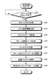
- FIG. 12 is a flowchart illustrating an example of a frame reception process procedure according to the first embodiment.
- the reception unit 40 stores the received serial data frame 130 in the reception buffer 41 (step S31), and the conversion unit 42 converts the received serial data frame 130 into a parallel data frame 130 (step S32). .
- the start flag detection unit 431 detects the start flag 132 by comparing the data output from the conversion unit 42 with the sequential start flag pattern (step S33). If the start flag 132 is not detected (No in step S33), detection is performed until the start flag 132 is detected. On the other hand, when the start flag 132 is detected (Yes in step S33), the start flag detection unit 431 outputs a start flag detection signal indicating that the start flag 132 has been detected, and the memory storage information extraction unit 432 is to start.
- the memory storage information extraction unit 432 extracts the memory storage information 133 from the time when the start flag 132 is detected (step S34). Since the lengths of the start flag 132 and the memory storage information 133 are determined, data of a predetermined length is acquired from the time when the start flag 132 is detected, and the length of the start flag 132 is removed from the head to store the memory storage information. 133 is obtained. After extracting the memory storage information 133, the memory storage information extraction unit 432 outputs a completion signal indicating that the extraction of the memory storage information has been completed.
- the transmission data extracting unit 433 extracts the data 135 (step S35).
- the extraction starts after the memory storage information 133, but the data 135 is obtained by removing the frame inspection data 136 and the end flag 138 of a certain length retroactive from the time when the end flag 138 of the frame is identified. Extract.
- the transmission data extraction unit 433 outputs a completion signal indicating the completion of data extraction.
- the frame inspection data extracting unit 434 extracts the frame inspection data 136 from the frame (step S36).
- extraction is started from the end of the data 135, and when the end flag 138 is identified, the frame check data 136 is extracted by excluding the end flag 138 having a certain length.
- the end flag extraction unit 435 detects the end flag 138 (step S37).
- the end flag 138 is detected by determining whether the data from the conversion unit 42 matches the end flag pattern, and the end of the frame is identified by matching the end flag pattern.
- the end flag extraction unit 435 activates the frame inspection processing unit 436.
- the frame inspection processing unit 436 inspects the received frame 130 (step S38). For example, frame check calculation such as CRC or checksum of the received frame 130 is performed and compared with the frame check data 136 extracted from the frame 130 to determine whether the received frame 130 is normal.
- frame check calculation such as CRC or checksum of the received frame 130 is performed and compared with the frame check data 136 extracted from the frame 130 to determine whether the received frame 130 is normal.
- the data storage processing unit 44 stores the data extracted by the transmission data extraction unit 433 in the buffer memory 45 based on the memory storage information 133 extracted by the memory storage information extraction unit 432 (step S39). Since the storage location (address) of the data 135 in the buffer memory 45 is defined in the memory storage information 133, the data 135 is stored in the storage location. Thus, the reception process ends.
- the data 135 is stored at a specific address in the buffer memory 45 according to the memory storage information 133 in the frame 130, it is possible to omit the conventionally required reception data abnormality analysis unit. In addition, it is possible to shorten the processing time at the time of reception. As a result, reception data processing can be simplified.
- the processing time required for the reception processing is shortened, and a shorter communication cycle can be realized.
- the communication cycle can be further shortened, the data update cycle between the devices can be increased, the data transmission time can be shortened, and the performance of the entire control device can be improved.
- the next normally received frame is stored at a specific address of the buffer memory 45 by the memory storage information 133. Therefore, it is possible to delete the process of searching for received data from the buffer memory 45 in the received data processing unit.
- FIG. FIG. 13 is a block diagram schematically showing the configuration of the receiving unit according to the second embodiment.
- the data storage processing unit 44A of the receiving unit 40A according to the second embodiment receives data when storing the data extracted from the frame in the buffer memory 45 based on the memory storage information extracted from the frame by the reception control unit 43.
- the reception data state indicating whether or not the frame from the frame inspection processing unit 436A of the control unit 43 is normally received is also acquired and stored in the buffer memory 45 together with the data as reception data.
- symbol as Embodiment 1 is attached
- the configuration of the transmission unit 30 is the same as that of the first embodiment, and therefore the description thereof is omitted.
- FIG. 14 is a diagram schematically showing an example of the state of the buffer memory of the controller according to the second embodiment.
- the addresses “0100h”, “0200h”, and “0300h” of the buffer memory 45 include the data extracted from the frames 111 to 113 received from the motor driving devices 12-1 to 12-3, and each frame.
- the received data states 111 to 113 are stored.
- the data reception state is stored at an address defined by the memory storage information, and the data is stored in the subsequent area.
- the controller 13 reads the received data states and data corresponding to the motor driving devices 12-1 to 12-3 from these fixed addresses in the buffer memory 45. Then, it is determined whether or not each of the frames 111 to 113 received from the received data state is normal. If the frames are received normally, the motor position and motor speed of each motor driving device 12-1 to 12-3 are determined from the data. Then, state data such as drive current, various control signals, and abnormal states are acquired. Further, when the data has not been received normally, the status data from the motor driving devices 12-1 to 12-3 is not acquired.
- the received data is stored in the specific address of the buffer memory 45 in accordance with the memory storage information in the frame, so that the received data state and the data extracted from the frame are stored.
- the received data state can be acquired to determine whether or not the data is abnormal.
- the effect that the time required to obtain the received data state can be shortened as compared with the conventional case can be obtained.
- the received data state is stored together with the received data at a specific address in the buffer memory 45, if one of the periodically received frames is not received, it is easily determined that a frame is missing. be able to. As a result, there is no need to perform a combination process of communication data information and reception data in the reception data processing unit as in the prior art.
- FIG. FIG. 15 is a block diagram schematically showing a configuration of a receiving unit according to the third embodiment.
- the receiving unit 40B of the third embodiment further includes a conversion table unit 46 that converts memory storage information extracted from the frame into a storage destination address for storing data in the buffer memory 45.
- the data storage processing unit 44B stores the data extracted by the reception control unit 43 and the received data state at the address output by the conversion table unit 46.
- symbol as Embodiment 1, 2 is attached
- the configuration of the transmission unit 30 is the same as that of the first embodiment, and therefore the description thereof is omitted.
- FIG. 16 is a diagram schematically illustrating an example of the configuration of the conversion table unit according to the third embodiment.
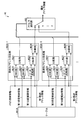
- the conversion table unit 46 stores a table 461 that shows the relationship between the memory storage information of the frame and the storage address information that is the storage destination address of the buffer memory 45, and the storage address that is the storage location of the received data in the buffer memory 45.
- the table 461 includes received storage information indicating the memory storage information to be received by itself, and storage address information for determining in which address of the buffer memory 45 the data in the frame having the memory storage information is stored. Is a memory location conversion information that defines the relationship between the received storage information and the storage address information, and outputs the same number of storage destination address generation units 462-1, 462-2,.
- FIG. 17 is a diagram schematically illustrating an example of a table configuration.
- the reception storage information of the table 461 is memory storage information that should be received by the own device (reception unit 40).
- One storage address information is an actual address in the buffer memory 45 assigned to the received storage information.
- the storage address information “A100h” is associated with the reception storage information “0100h” and “0700h”
- the storage address information “A200h” includes the reception storage information “0200h” and “0800h”.
- the storage address information “A300h” is associated with the reception storage information “0300h”.
- a plurality of pieces of received storage information are associated with the same address of one buffer memory 45.
- the address of the buffer memory 45 is set so that the data storage destination of the frame 111 and the data storage destination of the frame 112 in the first communication cycle are not stored at the same buffer memory 45 address.
- the received storage information is associated. Then, the received storage information in the table 461 is output to different storage destination address generation units 462-1, 462-2,.
- the storage destination address generation units 462-1, 462-2,... Have a comparison unit 4621 that compares the frame memory storage information with the received storage information referenced from the table 461.
- the comparison unit 4621 compares the memory storage information extracted from the frame by the reception control unit 43 with the reception storage information referenced from the table 461. If they match, a match signal is generated, and the storage address information referenced from the table 461 is output to the address selection unit 463 together with the match signal.
- As many storage address generation units 462-1, 462-2,... are provided as there are entries in the table 461, for example.
- the address selection unit 463 is selected from the storage destination address generation units 462-1, 462-2,... That output a match signal among the plurality of storage destination address generation units 462-1, 462-2,.
- Storage address information is selected and output to the data storage processing unit 44 as a storage destination address in the buffer memory 45.
- FIG. 18 is a diagram schematically showing an example of the state of the buffer memory of the controller according to the third embodiment.
- the addresses “A100h”, “A200h”, and “A300h” of the buffer memory 45 are stored in the frames 111 to 113 together with the data extracted from the frames 111 to 113 received from the motor driving devices 12-1 to 12-3.
- 113 reception data states are stored.
- the data reception state is stored at the address converted by the conversion table unit 46, and the data is stored in the subsequent area.
- Memory conversion information is input from the memory storage information extraction unit 432 to the conversion table unit 46.
- the memory storage information is input to the comparison units 4621 in all the storage destination address generation units 462-1, 462-2,.
- all the received storage information in the table 461 is input to the comparison unit 4621 in the different storage destination address generation units 462-1, 462-2,.
- the first reception storage information in the table 461 is input to the storage destination address generation unit 462-1
- the second reception storage information is input to the storage destination address generation unit 462-2
- One reception storage information in the table 461 is input to one storage destination address generation unit 462-1, 462-2,.
- the comparison unit 4621 of the storage destination address generation units 462-1, 462-2,... Compares the input memory storage information with the received storage information to determine whether they match. If they match, the comparison unit 4621 outputs a match signal to the address selection unit 463 and outputs storage address information referenced from the table 461. For example, the storage destination address generation unit 462-1 matches the memory storage information with the first reception storage information, and the other storage destination address generation units 462-2,. If not, only the comparison unit 4621 of the storage destination address generation unit 462-1 outputs a match signal. Further, the storage destination address generation units 462-1, 462-2,... Output the storage address information from the table 461 to the address selection unit 463.
- the address selection unit 463 selects storage address information from the storage destination address generation units 462-1, 462-2,... That output the coincidence signal, and stores the selected storage address information in the buffer memory 45.
- the data is output to the data storage processing unit 44 as a destination address.
- the address selection unit 463 selects the storage address information output from the storage destination address generation unit 462-1 as the storage destination address. To do. Thus, the storage destination address generation process ends.
- the conversion table unit 46 converts the storage destination of the buffer memory 45 for each frame, and one or more pieces of data exchanged at different communication cycles with respect to one address of the buffer memory 45 Since (multiple) data can be stored, it is possible to receive all frames with a smaller size of the buffer memory 45.
- Embodiment 4 FIG.
- the transmission unit in each unit has the same configuration as that of FIG. 5 of the first embodiment
- the reception unit of each unit has the same configuration as that of FIG. 15 of the third embodiment.
- the configuration of the conversion table unit 46 of the receiving unit 40 is different from that of the third embodiment.
- FIG. 19 is a diagram schematically illustrating an example of the configuration of the conversion table unit according to the fourth embodiment.
- the conversion table unit 46 generates a plurality of storages for generating a table 461A indicating the relationship between the memory storage information of the frame and the storage destination address of the buffer memory 45, and a storage address that is a storage position of the received data in the buffer memory 45. .. And destination address generators 462A-1, 462A-2,..., And an address selector 463 that selects a plurality of storage destination addresses.
- the table 461A includes reception storage information indicating memory storage information to be received by itself, comparison range information for determining a range in which the memory storage information and the reception storage information are compared, and a buffer memory of data in the frame having the memory storage information 45 is a table that defines the relationship between the address calculation information used for calculating the address within 45 and the storage address generation unit 462A as many as the number of pieces of information obtained by pairing the reception storage information, the comparison range information, and the address calculation information. -1,462A-2,...
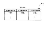
- FIG. 20 is a diagram schematically showing an example of a table configuration.
- the received storage information of the table 461A is the memory storage information of the frame that should be received by the own apparatus (reception unit 40), and is compared with the memory storage information of the received frame.
- the comparison range information has a mask function that determines a range in which the memory storage information (address) and the reception storage information (address) of the received frame are compared.
- the address calculation information is an actual address in the buffer memory 45 assigned to the received storage information. In this example, comparison storage information “FF00h” and address calculation information “A100h” are registered in association with reception storage information “0100h”.
- the storage destination address generation units 462A-1, 462A-2,... Have an AND unit 4622 that determines a comparison range of memory storage information, an AND unit 4623 that determines a comparison range of received storage information, and a comparison range is determined.
- a comparison unit 4621 that compares the stored memory information with the received storage information that is referenced from the table 461A and for which the comparison range is determined, a bit inversion unit 4624 that inverts the comparison range information, and a value that is added to the address calculation information.
- the AND units 4622 and 4623 and the comparison unit 4621 compare whether or not the memory storage information for which the comparison range is determined by the comparison range information matches the received storage information. Is output. Further, the bit inversion unit 4624, the AND unit 4625, and the addition unit 4626 add the memory storage information of the portion that is not set as the comparison range by the comparison range information, that is, masked by the comparison range information, and the address calculation information. As a result, the storage address of the data in the buffer memory 45 is generated.
- the address selection unit 463 is a storage destination address generation unit 462A-1, 462A-2,... That outputs a match signal among the plurality of storage destination address generation units 462A-1, 462A-2,.
- the generated storage address is selected and output to the data storage processing unit 44 as a storage address in the buffer memory 45.
- Memory conversion information is input from the memory storage information extraction unit 432 to the conversion table unit 46.
- the memory storage information is input to AND units 4622 and 4623 in all storage destination address generation units 462A-1, 462A-2,.
- the received storage information, the comparison range information, and the address calculation information in the table 461A are output as a pair to different storage destination address generation units 462A-1, 462A-2,.
- Received storage information is input to the AND unit 4623, and comparison range information is input to the AND units 4622, 4623 and the bit inversion unit 4624.
- the address calculation information is input to the adder 4626.
- the AND unit 4622 of the storage destination address generation units 462A-1, 462A-2,... The logical product of the memory storage information extracted from the frame by the reception control unit 43 and the comparison range information referenced from the table 461A.
- the information obtained by taking is taken as the first memory storage information.
- the AND unit 4623 uses the logical product of the reception storage information referenced from the table 461A and the comparison range information referenced from the table 461A as the comparison reception storage information.
- the comparison unit 4621 compares the first memory storage information and the comparison reception storage information output from the AND unit 4622 and the AND unit 4623, respectively, and outputs a match signal when the two match.
- the AND unit 4625 calculates the logical product of the inversion comparison range information obtained by bit-inversion of the comparison range information by the bit inversion unit 4624 and the memory storage information 133 and sets this as second memory storage information.
- the adder 4626 adds the second memory storage information and the address calculation information of the pair of information referred to from the table 461A, and sets this as a storage address. This storage address is output to the address selection unit 463 together with the coincidence signal.
- the address selection unit 463 selects a storage address from the storage destination address generation units 462A-1, 462A-2,... That output the coincidence signal, and a data storage processing unit as a storage destination address in the buffer memory 45 44, and the storage destination address generation process ends.
- the memory storage information extracted from the frame is ANDed with the comparison range information “FF00h” referenced from the table 461A by the AND unit 4622 of the storage destination address generation units 462A-1, 462A-2,.
- the lower byte of the memory storage information 133 input to the comparison unit 4621 is always “00h”.
- the received storage information “0100h” referenced from the table 461A is ANDed with the comparison range information “FF00h” by the AND unit 4623 of the storage destination address generation units 462A-1, 462A-2,.
- the lower 1 byte of the received storage information input to the comparison unit 4621 is always “00h”.
- all frames having memory storage information in the range of “0100h” to “01FFh” are received.
- the memory storage information 133 in the range of “0100h” to “01FFh” is represented by “A100h” using a pair of reception storage information, comparison range information, and address calculation information in the table of FIG. ”To“ A1FFh ”. That is, more address translations can be made while reducing the capacity of the table.
- the comparison unit 4621 outputs a coincidence signal for all the frames.
- the lower 1 byte output from the AND unit 4625 is “00h”, “20h”, and “60h”, respectively.
- the adder 4626 adds these and the address calculation information “A100h” of the table 461A to obtain “A100h”, “A120h”, and “A160h” as storage addresses, respectively, and the address selector 463 assigns these addresses to these addresses, respectively.
- the received data state and the data in the frame are stored.
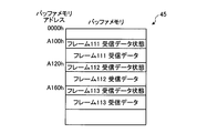
- FIG. 21 is a diagram schematically showing an example of the state of the buffer memory of the controller according to the fourth embodiment.
- the state in the buffer memory 45 of the controller 13 when each frame having “0100h”, “0120h”, and “0160h” as memory storage information is received is shown.
- the data of the frame having the memory storage information “0100h” is stored at the address “A010h” of the buffer memory 45 together with the received data state.
- the data of the frames having the memory storage information “0120h” and “0160h” are stored together with their received data states at addresses “A0120h” and “A0160h” of the buffer memory 45, respectively.
- the conversion table unit 46 is used when storing a plurality of frames in the buffer memory 45 by using a part of the memory storage information 133 as additional information of the storage address of the buffer memory 45.
- the amount of data to be registered in the table 461A can be minimized, and the storage destination address generation units 462A-1, 462A-2,. An address can be generated. That is, it is possible to reduce the amount of information necessary for the table 461A for determining the storage destination of the buffer memory 45.
- the circuit scale can be reduced, and when the storage destination address generation units 462A-1, 462A-2,. 462A-1, 462A-2,... Can be realized.
- the controller 13 and the motor driving devices 12-1 to 12-3 are daisy chain connected.
- the network topology is a star connection or a ring connection, each device is connected. Data can be transmitted and received in the same manner as described above, and the same effect as the above-described embodiment can be obtained.
- control device is used when a plurality of motor drive devices such as servo motors and induction motors are connected to a network and the plurality of motors are operated synchronously in accordance with a command from a controller connected to the network. Useful.
Landscapes
- Engineering & Computer Science (AREA)
- Theoretical Computer Science (AREA)
- Physics & Mathematics (AREA)
- General Engineering & Computer Science (AREA)
- General Physics & Mathematics (AREA)
- Medical Informatics (AREA)
- Computing Systems (AREA)
- General Health & Medical Sciences (AREA)
- Health & Medical Sciences (AREA)
- Computer Networks & Wireless Communication (AREA)
- Signal Processing (AREA)
- Quality & Reliability (AREA)
- Programmable Controllers (AREA)
- Communication Control (AREA)
- Information Transfer Systems (AREA)
- Computer And Data Communications (AREA)
- Small-Scale Networks (AREA)
- Synchronisation In Digital Transmission Systems (AREA)
Abstract
Priority Applications (7)
| Application Number | Priority Date | Filing Date | Title |
|---|---|---|---|
| JP2013500812A JP5496411B2 (ja) | 2011-02-25 | 2011-02-25 | 制御装置、制御システムおよび通信方法 |
| CN201180068453.2A CN103430510B (zh) | 2011-02-25 | 2011-02-25 | 控制装置、控制系统以及通信方法 |
| DE112011104950T DE112011104950T5 (de) | 2011-02-25 | 2011-02-25 | Steuervorrichtung, Steuersystem und Kommunikationsverfahren |
| KR1020137022365A KR101499375B1 (ko) | 2011-02-25 | 2011-02-25 | 제어 장치, 제어 시스템 및 통신 방법 |
| US13/980,109 US9141523B2 (en) | 2011-02-25 | 2011-02-25 | Control apparatus, control system, and communication method for controlling one or more motors in serial communication with a controller |
| PCT/JP2011/054394 WO2012114525A1 (fr) | 2011-02-25 | 2011-02-25 | Dispositif de commande, système de commande et procédé de communication |
| TW100129920A TWI499246B (zh) | 2011-02-25 | 2011-08-22 | 整體控制裝置、控制系統及通信方法 |
Applications Claiming Priority (1)
| Application Number | Priority Date | Filing Date | Title |
|---|---|---|---|
| PCT/JP2011/054394 WO2012114525A1 (fr) | 2011-02-25 | 2011-02-25 | Dispositif de commande, système de commande et procédé de communication |
Publications (1)
| Publication Number | Publication Date |
|---|---|
| WO2012114525A1 true WO2012114525A1 (fr) | 2012-08-30 |
Family
ID=46720339
Family Applications (1)
| Application Number | Title | Priority Date | Filing Date |
|---|---|---|---|
| PCT/JP2011/054394 Ceased WO2012114525A1 (fr) | 2011-02-25 | 2011-02-25 | Dispositif de commande, système de commande et procédé de communication |
Country Status (7)
| Country | Link |
|---|---|
| US (1) | US9141523B2 (fr) |
| JP (1) | JP5496411B2 (fr) |
| KR (1) | KR101499375B1 (fr) |
| CN (1) | CN103430510B (fr) |
| DE (1) | DE112011104950T5 (fr) |
| TW (1) | TWI499246B (fr) |
| WO (1) | WO2012114525A1 (fr) |
Cited By (1)
| Publication number | Priority date | Publication date | Assignee | Title |
|---|---|---|---|---|
| WO2022209054A1 (fr) * | 2021-03-31 | 2022-10-06 | パナソニックIpマネジメント株式会社 | Dispositif de communication, système de communication, procédé de commande de communication et programme |
Families Citing this family (6)
| Publication number | Priority date | Publication date | Assignee | Title |
|---|---|---|---|---|
| JP6552314B2 (ja) * | 2015-07-24 | 2019-07-31 | 日本電産サンキョー株式会社 | モータ制御装置 |
| JP6400770B1 (ja) * | 2017-04-03 | 2018-10-03 | 株式会社東芝 | 伝送局 |
| DE102017117288A1 (de) | 2017-07-31 | 2019-01-31 | Hengstler Gmbh | Datenübertragungsverfahren zwischen einem Drehwinkelgeber und einer Motorsteuereinrichtung oder einer Auswerteeinheit |
| JP6870568B2 (ja) * | 2017-10-24 | 2021-05-12 | オムロン株式会社 | 通信システム、制御装置、設定装置、設定方法およびプログラム |
| JP6919596B2 (ja) * | 2018-03-01 | 2021-08-18 | オムロン株式会社 | 計測システムおよび方法 |
| CN112154615B (zh) * | 2018-05-10 | 2023-09-29 | 三菱电机株式会社 | 电子控制装置 |
Citations (6)
| Publication number | Priority date | Publication date | Assignee | Title |
|---|---|---|---|---|
| JPS6129242A (ja) * | 1984-07-19 | 1986-02-10 | Nec Corp | 通信制御装置 |
| JPS62274851A (ja) * | 1986-05-21 | 1987-11-28 | Nippon Denso Co Ltd | シリアル通信制御装置 |
| JPH0690256A (ja) * | 1992-07-02 | 1994-03-29 | Internatl Business Mach Corp <Ibm> | パケット通信方法ならびにその送信装置および受信装置 |
| JPH09269934A (ja) * | 1996-04-02 | 1997-10-14 | Hitachi Ltd | 共有メモリのデータ一致化方法および伝送システム |
| WO2001002918A1 (fr) * | 1999-07-06 | 2001-01-11 | Mitsubishi Denki Kabushiki Kaisha | Systeme de commande d'entrainement |
| JP2003271209A (ja) * | 2002-03-15 | 2003-09-26 | Omron Corp | 制御装置並びに拡張機器及びプログラミングツール |
Family Cites Families (20)
| Publication number | Priority date | Publication date | Assignee | Title |
|---|---|---|---|---|
| JPS62103745A (ja) * | 1985-10-31 | 1987-05-14 | Kokusai Electric Co Ltd | デ−タ通信の送,受信制御回路 |
| JPS6384346A (ja) * | 1986-09-29 | 1988-04-14 | Toshiba Corp | 通信デ−タ制御装置 |
| JP2520905B2 (ja) | 1987-05-27 | 1996-07-31 | 株式会社日立製作所 | シリアル通信制御装置 |
| JP3012414B2 (ja) * | 1992-10-23 | 2000-02-21 | 日本電気通信システム株式会社 | 制御チャネル干渉検出方式 |
| JPH07244623A (ja) * | 1994-03-03 | 1995-09-19 | Fuji Electric Co Ltd | 伝送制御装置 |
| JPH09114729A (ja) | 1995-10-23 | 1997-05-02 | Fuji Electric Co Ltd | データ通信装置のメモリ割付方法及び通信方法 |
| JPH1132100A (ja) | 1997-07-10 | 1999-02-02 | Fujitsu Ltd | データ送受信方法及びデータ送受信装置 |
| JP2000148442A (ja) | 1998-11-09 | 2000-05-30 | Sony Corp | 提供媒体、並びにデータ処理装置およびデータ処理方法 |
| JP2000349853A (ja) * | 1999-06-01 | 2000-12-15 | Victor Co Of Japan Ltd | データ伝送方法 |
| US6393544B1 (en) * | 1999-10-31 | 2002-05-21 | Institute For The Development Of Emerging Architectures, L.L.C. | Method and apparatus for calculating a page table index from a virtual address |
| US6775802B2 (en) * | 2000-08-08 | 2004-08-10 | Qualcomm Incorporated | Method, apparatus, and system for signal prediction |
| JP4315626B2 (ja) * | 2001-11-16 | 2009-08-19 | シャープ株式会社 | データ駆動型情報処理装置のメモリ制御部における情報処理方法 |
| AU2003215864A1 (en) * | 2002-04-18 | 2003-10-27 | Koninklijke Philips Electronics N.V. | Read-only record carrier with recordable area in subcode channel |
| JP2003346273A (ja) * | 2002-05-30 | 2003-12-05 | Okuma Corp | センサー装置およびセンサー装置の検出データを用いて制御対象を制御するシステムの監視方法 |
| JP2004165764A (ja) | 2002-11-11 | 2004-06-10 | Matsushita Electric Ind Co Ltd | 多重伝送システム、多重装置及び分離装置 |
| JP4398836B2 (ja) * | 2004-09-30 | 2010-01-13 | ボッシュ株式会社 | 車両駆動制御方法及び車両駆動制御装置 |
| CN101401000B (zh) * | 2006-03-28 | 2012-08-22 | 泰尔茂株式会社 | 体液成分测定设备 |
| JP4845674B2 (ja) | 2006-10-26 | 2011-12-28 | キヤノン株式会社 | データ処理装置及び方法、通信装置、並びにプログラム |
| JP2009157493A (ja) * | 2007-12-25 | 2009-07-16 | Sharp Corp | データ転送制御装置及びicカード |
| WO2010027064A1 (fr) * | 2008-09-04 | 2010-03-11 | 日本電気株式会社 | Procédé de transmission de données, système de transmission de données, dispositif de transmission de données, dispositif de réception de données et programme de commande |
-
2011
- 2011-02-25 CN CN201180068453.2A patent/CN103430510B/zh active Active
- 2011-02-25 WO PCT/JP2011/054394 patent/WO2012114525A1/fr not_active Ceased
- 2011-02-25 DE DE112011104950T patent/DE112011104950T5/de not_active Withdrawn
- 2011-02-25 KR KR1020137022365A patent/KR101499375B1/ko active Active
- 2011-02-25 US US13/980,109 patent/US9141523B2/en active Active
- 2011-02-25 JP JP2013500812A patent/JP5496411B2/ja active Active
- 2011-08-22 TW TW100129920A patent/TWI499246B/zh active
Patent Citations (6)
| Publication number | Priority date | Publication date | Assignee | Title |
|---|---|---|---|---|
| JPS6129242A (ja) * | 1984-07-19 | 1986-02-10 | Nec Corp | 通信制御装置 |
| JPS62274851A (ja) * | 1986-05-21 | 1987-11-28 | Nippon Denso Co Ltd | シリアル通信制御装置 |
| JPH0690256A (ja) * | 1992-07-02 | 1994-03-29 | Internatl Business Mach Corp <Ibm> | パケット通信方法ならびにその送信装置および受信装置 |
| JPH09269934A (ja) * | 1996-04-02 | 1997-10-14 | Hitachi Ltd | 共有メモリのデータ一致化方法および伝送システム |
| WO2001002918A1 (fr) * | 1999-07-06 | 2001-01-11 | Mitsubishi Denki Kabushiki Kaisha | Systeme de commande d'entrainement |
| JP2003271209A (ja) * | 2002-03-15 | 2003-09-26 | Omron Corp | 制御装置並びに拡張機器及びプログラミングツール |
Cited By (4)
| Publication number | Priority date | Publication date | Assignee | Title |
|---|---|---|---|---|
| WO2022209054A1 (fr) * | 2021-03-31 | 2022-10-06 | パナソニックIpマネジメント株式会社 | Dispositif de communication, système de communication, procédé de commande de communication et programme |
| JPWO2022209054A1 (fr) * | 2021-03-31 | 2022-10-06 | ||
| JP7738225B2 (ja) | 2021-03-31 | 2025-09-12 | パナソニックIpマネジメント株式会社 | 通信装置、通信システム、通信制御方法及びプログラム |
| US12425261B2 (en) | 2021-03-31 | 2025-09-23 | Panasonic Intellectual Property Management Co., Ltd. | Communication device, communication system, and communication control method |
Also Published As
| Publication number | Publication date |
|---|---|
| CN103430510A (zh) | 2013-12-04 |
| JPWO2012114525A1 (ja) | 2014-07-07 |
| JP5496411B2 (ja) | 2014-05-21 |
| CN103430510B (zh) | 2016-06-29 |
| US20130297897A1 (en) | 2013-11-07 |
| TW201236413A (en) | 2012-09-01 |
| TWI499246B (zh) | 2015-09-01 |
| KR101499375B1 (ko) | 2015-03-05 |
| US9141523B2 (en) | 2015-09-22 |
| KR20130135898A (ko) | 2013-12-11 |
| DE112011104950T5 (de) | 2013-11-28 |
Similar Documents
| Publication | Publication Date | Title |
|---|---|---|
| JP5496411B2 (ja) | 制御装置、制御システムおよび通信方法 | |
| JP3392876B2 (ja) | 複数の遠心機を制御するためのインターリーブされたデータ通信システム | |
| CN103262405B (zh) | 可在操作中重构的控制系统以及用于其的方法 | |
| KR101259133B1 (ko) | 동작 중 재구성이 가능한 제어 시스템 및 그 방법 | |
| WO2019155700A1 (fr) | Système d'asservissement, concentrateur de capteurs et procédé de diagnostic de dispositif industriel | |
| CN104144094B (zh) | 数字总线系统从属节点及其操作方法 | |
| CN110457744B (zh) | 一种sd/sdio设备仿真模型框架及其设计方法 | |
| CN106776329B (zh) | 储能变流器的调试方法和调试设备 | |
| US20090248889A1 (en) | Serial attached scsi and serial ata wide port tunnelling through a fibre channel connection | |
| US10715796B2 (en) | Method and device for monitoring an image sensor | |
| US9122500B2 (en) | Method for preconfiguring an appliance, and method for starting up the appliance | |
| JP4902823B1 (ja) | 通信装置 | |
| WO2026026164A1 (fr) | Procédé et appareil de diagnostic de moteur, dispositif de diagnostic de moteur et système de diagnostic de moteur | |
| JP2019030025A (ja) | イーサネット(登録商標)フレーム検知回路 | |
| JP2014064452A (ja) | 多軸制御システム及び多軸制御方法 | |
| CN103957070B (zh) | 一种数据帧的定位方法及装置 | |
| CN116886247B (zh) | 基于uart通信的波特率自适应方法、装置、uart系统、介质 | |
| US9647853B2 (en) | Transmitting system, the device and the method for the remote bus | |
| CN117687851A (zh) | 服务器硬件测试方法、装置、电子设备和存储介质 | |
| US20090248884A1 (en) | Distance extender for serial attached scsi and serial ata | |
| US20150215136A1 (en) | Network control device, the network control system and the method of the remote device | |
| CN109845155B (zh) | 将数据分组从传感器传输到控制器的方法、传感器和控制器 | |
| KR101778330B1 (ko) | Plc 시스템의 베이스 상태 진단용 기능 모듈 | |
| JP2710175B2 (ja) | データ正誤判定器 | |
| CN110417762B (zh) | 一种具有报文打包技术的模块集成系统 |
Legal Events
| Date | Code | Title | Description |
|---|---|---|---|
| 121 | Ep: the epo has been informed by wipo that ep was designated in this application |
Ref document number: 11859039 Country of ref document: EP Kind code of ref document: A1 |
|
| ENP | Entry into the national phase |
Ref document number: 2013500812 Country of ref document: JP Kind code of ref document: A |
|
| WWE | Wipo information: entry into national phase |
Ref document number: 13980109 Country of ref document: US |
|
| ENP | Entry into the national phase |
Ref document number: 20137022365 Country of ref document: KR Kind code of ref document: A |
|
| WWE | Wipo information: entry into national phase |
Ref document number: 112011104950 Country of ref document: DE Ref document number: 1120111049501 Country of ref document: DE |
|
| 122 | Ep: pct application non-entry in european phase |
Ref document number: 11859039 Country of ref document: EP Kind code of ref document: A1 |