WO2012114874A1 - 電子部品の実装構造 - Google Patents
電子部品の実装構造 Download PDFInfo
- Publication number
- WO2012114874A1 WO2012114874A1 PCT/JP2012/052837 JP2012052837W WO2012114874A1 WO 2012114874 A1 WO2012114874 A1 WO 2012114874A1 JP 2012052837 W JP2012052837 W JP 2012052837W WO 2012114874 A1 WO2012114874 A1 WO 2012114874A1
- Authority
- WO
- WIPO (PCT)
- Prior art keywords
- ceramic
- metal substrate
- thermistor
- ceramic layer
- semiconductor
- Prior art date
- Legal status (The legal status is an assumption and is not a legal conclusion. Google has not performed a legal analysis and makes no representation as to the accuracy of the status listed.)
- Ceased
Links
Images



Classifications
-
- H—ELECTRICITY
- H10—SEMICONDUCTOR DEVICES; ELECTRIC SOLID-STATE DEVICES NOT OTHERWISE PROVIDED FOR
- H10N—ELECTRIC SOLID-STATE DEVICES NOT OTHERWISE PROVIDED FOR
- H10N10/00—Thermoelectric devices comprising a junction of dissimilar materials, i.e. devices exhibiting Seebeck or Peltier effects
- H10N10/80—Constructional details
-
- H—ELECTRICITY
- H01—ELECTRIC ELEMENTS
- H01C—RESISTORS
- H01C7/00—Non-adjustable resistors formed as one or more layers or coatings; Non-adjustable resistors made from powdered conducting material or powdered semi-conducting material with or without insulating material
- H01C7/008—Thermistors
-
- H—ELECTRICITY
- H01—ELECTRIC ELEMENTS
- H01C—RESISTORS
- H01C1/00—Details
- H01C1/01—Mounting; Supporting
- H01C1/012—Mounting; Supporting the base extending along and imparting rigidity or reinforcement to the resistive element
-
- H—ELECTRICITY
- H01—ELECTRIC ELEMENTS
- H01C—RESISTORS
- H01C17/00—Apparatus or processes specially adapted for manufacturing resistors
- H01C17/06—Apparatus or processes specially adapted for manufacturing resistors adapted for coating resistive material on a base
- H01C17/065—Apparatus or processes specially adapted for manufacturing resistors adapted for coating resistive material on a base by thick film techniques, e.g. serigraphy
- H01C17/06506—Precursor compositions therefor, e.g. pastes, inks, glass frits or green body
- H01C17/06513—Precursor compositions therefor, e.g. pastes, inks, glass frits or green body characterised by the resistive component
- H01C17/06533—Precursor compositions therefor, e.g. pastes, inks, glass frits or green body characterised by the resistive component composed of oxides
-
- H—ELECTRICITY
- H01—ELECTRIC ELEMENTS
- H01C—RESISTORS
- H01C7/00—Non-adjustable resistors formed as one or more layers or coatings; Non-adjustable resistors made from powdered conducting material or powdered semi-conducting material with or without insulating material
- H01C7/04—Non-adjustable resistors formed as one or more layers or coatings; Non-adjustable resistors made from powdered conducting material or powdered semi-conducting material with or without insulating material having negative temperature coefficient
- H01C7/042—Non-adjustable resistors formed as one or more layers or coatings; Non-adjustable resistors made from powdered conducting material or powdered semi-conducting material with or without insulating material having negative temperature coefficient mainly consisting of inorganic non-metallic substances
-
- H—ELECTRICITY
- H10—SEMICONDUCTOR DEVICES; ELECTRIC SOLID-STATE DEVICES NOT OTHERWISE PROVIDED FOR
- H10N—ELECTRIC SOLID-STATE DEVICES NOT OTHERWISE PROVIDED FOR
- H10N10/00—Thermoelectric devices comprising a junction of dissimilar materials, i.e. devices exhibiting Seebeck or Peltier effects
- H10N10/01—Manufacture or treatment
-
- H—ELECTRICITY
- H01—ELECTRIC ELEMENTS
- H01C—RESISTORS
- H01C1/00—Details
- H01C1/14—Terminals or tapping points specially adapted for resistors; Arrangements of terminals or tapping points on resistors
- H01C1/1413—Terminals or electrodes formed on resistive elements having negative temperature coefficient
-
- H—ELECTRICITY
- H01—ELECTRIC ELEMENTS
- H01C—RESISTORS
- H01C1/00—Details
- H01C1/14—Terminals or tapping points specially adapted for resistors; Arrangements of terminals or tapping points on resistors
- H01C1/142—Terminals or tapping points specially adapted for resistors; Arrangements of terminals or tapping points on resistors the terminals or tapping points being coated on the resistive element
-
- H—ELECTRICITY
- H01—ELECTRIC ELEMENTS
- H01C—RESISTORS
- H01C7/00—Non-adjustable resistors formed as one or more layers or coatings; Non-adjustable resistors made from powdered conducting material or powdered semi-conducting material with or without insulating material
- H01C7/04—Non-adjustable resistors formed as one or more layers or coatings; Non-adjustable resistors made from powdered conducting material or powdered semi-conducting material with or without insulating material having negative temperature coefficient
Definitions
- the present invention relates to a thermistor and a manufacturing method thereof, and more particularly, to a thermistor in which a metal substrate, a thermistor thin film layer, and an electrode are laminated, and a manufacturing method thereof.
- Patent Document 1 an NTC thermistor or a PTC thermistor used as a temperature sensor or the like in a protection circuit is known as disclosed in Patent Document 1.
- the thermistor disclosed in Patent Document 1 includes a flat metal substrate that also serves as an electrode, a temperature-sensitive resistor film formed on one main surface thereof, and one electrode film formed on the temperature-sensitive resistor film. Become.
- the thermistor described above has a structure in which a flat metal substrate is used as one electrode and one electrode film formed in the uppermost layer is used as the other electrode. For this reason, when this thermistor is mounted on a substrate or the like, electrical connection to the electrode film has to be performed by wire bonding, and mounting in a very small space is impossible.
- a thermistor is used as a temperature sensor for an IC component mounted on a printed wiring board, a minute gap of 150 to 200 ⁇ m is generated between the printed wiring board and the IC component. Is preferably mounted in this gap.
- mounting by wire bonding mounting in such a minute gap is substantially difficult.
- a temperature sensitive resistor film is formed on a wiring board by sputtering.
- the bonding property to the flat metal substrate can be obtained, but the sputtering method is costly for manufacturing equipment and is not suitable for mass production. Therefore, it is required to be formed by a solid phase method.
- the thermal expansion coefficients of the flat metal substrate and the temperature-sensitive resistor film are different, so that the shrinkage rates are different. For this reason, even if the flat metal substrate and the temperature-sensitive resistor film can be bonded, the adhesion strength at the bonding interface may be insufficient depending on the external environment.
- an object of the present invention is to provide a thermistor that can be mounted with solder and has excellent adhesion strength even when formed by a solid phase method, and a method for manufacturing the thermistor.
- a first invention of the present invention includes a metal substrate, a semiconductor ceramic layer formed on the metal substrate by a solid-phase method, and a pair of divided electrodes formed on the semiconductor layer. Contains ceramic particles, and the thickness direction of the metal substrate is not divided by the columnar structure in which the ceramic particles or ceramic particles are continuously formed.
- the present inventor has a metal substrate, a semiconductor ceramic layer formed on the metal substrate, and a pair of divided electrodes formed on the semiconductor ceramic layer. I designed a thermistor. With the shape as described above, solder mounting can be performed on the printed wiring board by a method such as reflow. Further, the thin semiconductor ceramic layer and the metal substrate are integrally fired.
- the metal base material and the semiconductor ceramic layer have different coefficients of thermal expansion, so that the shrinkage rate is different even when integrally fired. For this reason, even if the metal base material and the semiconductor ceramic layer can be joined, for example, moisture enters the joint interface in a high temperature and high humidity environment, and the joint between the metal base material and the semiconductor ceramic layer is divided. As a result, the resistance value changes greatly.
- this invention it became clear by mixing ceramic powder with a metal base material that the adhesive strength of a semiconductor ceramic layer and a metal base material improves. This seems to contribute to the anchor effect by the ceramic powder and the increased contact area between the semiconductor ceramic layer and the metal substrate.
- the metal base is not divided in the thickness direction due to the ceramic particles contained in the metal base or the column structure in which the ceramic particles are continuously formed, the flexibility of the metal base is not lost.
- the adhesion strength between the metal substrate and the semiconductor ceramic layer is improved without impairing the above.
- the metal substrate is divided in the thickness direction by the ceramic particle or the column structure of ceramic particles means that the same ceramic particle or column structure of ceramic particles is exposed on the front and back surfaces of the metal substrate.
- the thickness of the metal substrate of the electronic component is preferably 10 to 80 ⁇ m, and the thickness of the ceramic layer is preferably 1 to 10 ⁇ m (second invention).
- the metal substrate and the ceramic layer are preferably formed in a sheet shape (third invention).
- the ceramic particles are preferably 16 vol% or more and 40 vol% or less with respect to the metal substrate (fifth invention).
- the semiconductor ceramic layer is preferably made of an NTC ceramic material, and the ceramic particles are preferably the same material as the semiconductor ceramic layer or an iron oxide compound (sixth invention).
- the adhesion strength between the metal substrate and the semiconductor ceramic layer is improved without affecting the characteristics of the semiconductor ceramic layer and without losing flexibility.
- the divided electrode preferably contains ceramic particles (seventh invention).
- the adhesion strength between the semiconductor ceramic layer and the divided electrode is improved, which is more preferable.
- An eighth invention of the present invention is a method for manufacturing a thermistor comprising a metal substrate, a semiconductor ceramic layer formed on the metal substrate, and a pair of split electrodes formed on the semiconductor ceramic layer.
- a step of applying a ceramic slurry on a carrier film to a predetermined thickness to form a ceramic green sheet to be a semiconductor ceramic layer; and a metal paste containing ceramic powder on the ceramic green sheet to a predetermined thickness Applying the electrode paste to a predetermined thickness on the surface of the ceramic green sheet that faces the surface on which the metal substrate sheet is formed
- the ceramic powder becomes ceramic particles at the interface between the metal base and the semiconductor ceramic layer.
- the ceramic particles make irregularities on the surface, and the adhesion strength is improved by the anchor effect or the increase of the contact area.
- the ceramic powder is contained in the metal base sheet in the range of 16 vol% or more and 40 vol% or less (9th invention).
- a thermistor with improved adhesion strength between the metal substrate and the semiconductor ceramic layer can be provided without impairing the flexibility of the thermistor.
- the electrode paste also contains ceramic powder (tenth invention).
- a thermistor having improved adhesion strength between the semiconductor ceramic layer and the divided electrodes can be provided.
- a thermistor having excellent adhesion strength and a manufacturing method can be provided even if it can be mounted with solder and formed by a solid phase method.
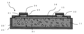
- FIG. 1 is a sectional view of a flexible thermistor according to a first embodiment of the present invention.
- the mounting structure of the flexible thermistor 1A of the present invention includes a metal base 11, a semiconductor ceramic layer 15 formed on the metal base 11, a pair of divided electrodes 21 and 22 formed on the semiconductor ceramic layer 15, And a flexible thermistor 1A.
- a Ni plating film 23 and a Sn plating film 24 are sequentially formed on the surfaces of the divided electrodes 21 and 22.
- An Ni plating film 23 ′ and an Sn plating film 24 ′ are also formed on the surface of the metal base 11.
- the protective layer 16 is formed on the surface of the semiconductor ceramic layer 15. This protective layer is not necessarily formed.
- the metal substrate 11 is obtained by firing a sheet-like formed body of metal powder paste
- the semiconductor ceramic layer 15 is obtained by firing a ceramic slurry or a sheet-like formed body of ceramic paste
- the divided electrodes 21 and 22 are made of electrode material paste. It is fired.
- the metal powder paste sheet-shaped body, the ceramic slurry sheet-shaped body and the electrode paste are obtained by integrally firing these three. Note that at least the metal substrate 11 and the semiconductor ceramic layer 15 may be integrally fired.
- the thickness of the metal substrate 11 is about 10 to 80 ⁇ m
- the thickness of the semiconductor ceramic layer 15 is about 1 to 10 ⁇ m
- the thickness of the divided electrodes 21 and 22 is about 0.1 to 10 ⁇ m
- the total thickness of the flexible thermistor 1A is 10 to 10 ⁇ m. It is about 100 ⁇ m.
- a ceramic material having NTC characteristics including an appropriate amount of Mn, Ni, Fe, Ti, Co, Al, Zn, etc. in any combination can be used.
- the oxide of the transition metal element is used for mixing, but carbonate, hydroxide, or the like of the element may be used as a starting material.
- a noble metal such as Ag, Pd, Pt, or Au, or a base metal such as Cu, Ni, Al, W, or Ti, or an alloy containing them can be used. .
- the metal base material 11 contains ceramic particles 30, and the thickness direction of the metal base material 11 is not divided by the columnar structure 31 in which the ceramic particles 30 or the ceramic particles are continuously formed.
- the ceramic particles 30 are preferably about 0.1 ⁇ m to 3.0 ⁇ m, and when these ceramic particles 30 are contained in a metal paste as a metal substrate and fired, a plurality of ceramic particles 30 are connected in a column structure. Even if the structure 31 is not formed or the column structure 31 is formed, the metal base material 11 is formed so as not to be divided in the thickness direction.
- the thermistor 1A By having such a configuration, it is possible to provide the thermistor 1A with improved adhesion strength between the metal substrate 11 and the semiconductor ceramic layer 15 without impairing the flexibility as the flexible thermistor 1A.
- the ceramic particles 30 are preferably included in the range of 16 vol% or more and 40 vol% or less with respect to the metal substrate 11.
- the amount is less than 16 vol%, the presence ratio of the ceramic particles 30 contained in the metal base material 11 is small, so that there are cases where sufficient adhesion strength cannot be obtained under severe conditions such as high temperature and high humidity. .
- the column structure 31 in which the ceramic particle 30 is continuously formed is likely to occur, and the column structure 30 is likely to be continuous in the thickness direction of the metal substrate 11. As a result, there is a possibility that the flexibility of the metal substrate 11 may be hindered.
- the ceramic particles 30 are preferably made of the same or similar material as that used for the semiconductor ceramic layer 15.
- the ceramic particles 30 may be oxides of Mn 3 O 4 , NiO, Fe 2 O 3 , TiO 2 , or These mixed oxides are preferably used.
- the material used for the semiconductor ceramic layer 15 is used, the possibility that the characteristic layer of the semiconductor ceramic layer 15 is adversely affected is low.
- the semiconductor ceramic layer 15 is a material that is significantly eroded by plating
- the material used for the protective layer 16 may be used.
- the Ni plating film 23 ′ and the Sn plating film 24 ′ are also formed on the surface of the metal substrate 11.
- the Ni plating film 23 and the Sn plating film 24 are formed on the surfaces of the divided electrodes 21 and 22 by electroplating. By doing so, it is inevitably formed on the surface of the metal substrate 11 made of metal, and it is not always necessary to form it.
- FIG. 2 is an equivalent circuit of the flexible thermistor 1A.
- the divided electrodes 21 and 22 serve as input / output terminals, and the resistors R1 and R2 are formed of the semiconductor ceramic layer 15 and are electrically connected in series via the metal base 11. That is, the thermistor circuit is configured by the resistors R1 and R2 by the semiconductor ceramic layer 15 sandwiched in the thickness direction between the divided electrodes 21 and 22 and the metal substrate 11.
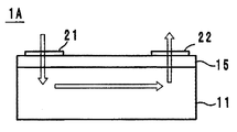
- FIG. 3 is a diagram showing a path of a current flowing through the flexible thermistor 1A. Since the divided electrodes 21 and 22 are formed on the surface of the semiconductor ceramic layer 15, as shown by the arrows in FIG. 3, the portions that are in contact with the divided electrodes 21 and 22 are passed through the metal substrate 11. Current flows through the path.
- a crack is likely to occur in the central portion of the semiconductor ceramic layer 15. However, even if a crack occurs in the central portion of the semiconductor ceramic layer 15, that portion is not a current-carrying path and therefore does not affect the electrical characteristics of the flexible thermistor 1 ⁇ / b> A.
- a metal base sheet that becomes a metal base 11 having a thickness of 5 to 100 ⁇ m after firing a paste for a metal base containing Ag—Pd as a main component and containing ceramic powder as ceramic particles by a doctor blade method Form.
- an oxide such as Mn—Ni—Fe—Ti is weighed so as to have a predetermined composition (targeting to have a resistivity of 10 4 ⁇ cm).
- a pulverizing medium it is sufficiently wet pulverized by a ball mill, and then calcined at a predetermined temperature to obtain a ceramic powder.
- An organic binder is added to the ceramic powder, and wet mixing is performed to obtain a semiconductor ceramic paste.
- a semiconductor ceramic layer 15 is formed from the obtained semiconductor ceramic paste by a screen printing method or the like.
- an organic binder is added to an insulating material such as Fe 2 O 3 to form a paste, and only a portion where the divided electrodes 21 and 22 are connected is exposed by a screen printing method or the like to form the protective layer 16. .
- an Ag—Pd paste to be the divided electrodes 21 and 22 is screen-printed so as to be connected to the semiconductor ceramic layer 15 exposed from the protective layer 16 to obtain a laminate.
- the mother sheet of the obtained laminate is cut into individual thermistors.
- the obtained 1 unit piece is accommodated in a thermistor zirconia cage, subjected to binder removal treatment, and then fired at a predetermined temperature (for example, 900 to 1300 ° C.).
- an Ni plating film 23 and an Sn plating film 24 are sequentially formed by electroplating.
- a screen printing method is generally used, but gravure printing, an ink jet method, a doctor blade method, or the like may be used.
- the metal substrate 11 can also be formed by a printing method such as screen printing.
- the divided electrodes 21 and 22 can be formed by screen printing, sputtering, vapor deposition, or the like.
- Example 1 In Experimental Example 1, the first embodiment described with reference to FIG. 1 was evaluated.
- Mn 3 O 4 , NiO, Fe 2 O 3 , and TiO 2 are weighed so that the resistivity is 10 4 ⁇ cm, and sufficiently wet pulverized with a ball mill using a pulverizing medium such as zirconia. And calcining at 700 ° C. for 2 hours to obtain a ceramic calcined powder made of an oxide of Mn—Ni—Fe—Ti.
- the ceramic powder as a co-material shown in Table 1 prepared in the same manner as the ceramic calcined powder in the Ag-Pd metal paste mixed so as to be Ag 90 wt% Pd 10 wt% is shown in Table 1. Mixed at the indicated ratio. Then, a metal base sheet having a thickness after firing of 30 ⁇ m was formed on a PET carrier sheet by a doctor blade method using the obtained metal paste.
- a sheet-like semiconductor ceramic pattern was formed on the metal base sheet so that the thickness after firing the above-described semiconductor ceramic paste by screen printing was 3 ⁇ m. Further, on this, a sheet-like protective layer pattern made of Fe 2 O 3 having excellent plating resistance is formed so that the thickness after firing becomes 10 ⁇ m except for a region that is slightly smaller than the region where the divided electrodes are formed. Formed. Subsequently, a divided electrode pattern was formed so that the same metal paste as the metal paste used for the metal substrate had a thickness after firing of 3 ⁇ m. The obtained metal base sheet, sheet-like semiconductor ceramic pattern, sheet-like protective layer pattern, and divided electrode pattern were degreased and then integrally fired at 950 ° C. for 2 hours. Thereby, the thermistor in which the metal substrate, the semiconductor ceramic layer, the protective layer, and the divided electrode layer were sequentially formed was obtained.
- Ni and Sn plating were sequentially formed on the obtained thermistor by electrolytic plating. Thereby, Ni and Sn plating are formed on the surface of the divided electrode and the surface of the metal substrate. Then, it was mounted on a land of a glass epoxy substrate with Sn—Ag—Cu lead-free solder.
- Example 2 In order to measure the adhesion strength between the semiconductor ceramic layer and the metal substrate more quantitatively, a test piece 40 as shown in FIG. 4 was prepared. Specifically, a slurry for forming a sheet was prepared from the semiconductor ceramic powder used for preparing the thermistor of Experimental Example 1, and a ceramic green sheet was obtained using a doctor blade. The green sheet was cut into a predetermined size to obtain a plurality of ceramic green sheets. Subsequently, the same metal paste used for the metal base sheet of Experimental Example 1 is printed on one ceramic green sheet by screen printing, and the ceramic green sheet is sandwiched between a plurality of ceramic green sheets from both sides. Thereby, the flat laminated block body in which the metal paste was sandwiched one layer was formed.
- test piece 40 square columnar sample 40 of ⁇ 1.0 mm ⁇ length 5.0 mm in which the metal layer 42 was disposed between the ceramics 41.
- Example 3 Then, the following evaluation was performed about the flexibility of the metal base material by co-material addition. Specifically, a sample for deflection test was prepared, in which the ceramic green sheet obtained in Experimental Example 1 and the metal sheet added with the common material obtained in Experimental Example 1 were laminated and integrally fired. This length is 50 mm ⁇ width 5 mm, the thickness of the metal substrate is 30 ⁇ m, and the thickness of the semiconductor ceramic layer is 2 ⁇ m.
- the deflection test sample obtained above was placed on a cylinder having a diameter of 10.13 cm, 5.07 cm, 1.30 cm, and 0.71 cm corresponding to the amount of warpage of the thermistor at the deflection amounts of 1 mm, 2 mm, 8 mm, and 16 mm.
- the presence or absence of destruction of the sample for winding and a deflection test was confirmed.
- As a result of winding the sample for deflection test around the cylinder it was evaluated as x when a crack was generated in the metal base material, and when it did not occur, it was evaluated as ⁇ .
- the number of samples was five, and when even one crack occurred, it was marked as x. Table 3 shows the experimental results.
- B25 / B50 (K) In (R25 / R50) / ((1 / 273.15 + 25) ⁇ 1 / (273.15 + 50)) The number of samples was 10, which was the average value. Table 4 shows the experimental results.
Landscapes
- Engineering & Computer Science (AREA)
- Microelectronics & Electronic Packaging (AREA)
- Physics & Mathematics (AREA)
- Electromagnetism (AREA)
- Manufacturing & Machinery (AREA)
- Thermistors And Varistors (AREA)
- Apparatuses And Processes For Manufacturing Resistors (AREA)
Abstract
Description
図1は、この発明の第1の実施形態によるフレキシブルサーミスタの断面図である。
実験例1においては、図1を参照して説明した第1の実施形態についての評価を行なった。

より定量的に半導体セラミック層と金属基材との密着強度を測定するために、図4に示されるような試験片40を作製した。具体的には、実験例1のサーミスタを作製するために使用した半導体セラミック粉末にてシート成形用のスラリーを作製し、ドクターブレードによりセラミックグリーンシートを得た。そして、このグリーンシートを所定寸法に裁断して複数枚のセラミックグリーンシートを得た。続いて、実験例1の金属基材シートに用いたものと同一の金属ペーストを、1枚のセラミックグリーンシートにスクリーン印刷によって印刷し、そのセラミックグリーンシートを両側から複数のセラミックグリーンシートで挟持することで金属ペーストが一層挟まれた平板状の積層ブロック体を形成した。続いて、これを圧着した後に、950℃で2時間焼成した。得られた試料をダイシングカットし、セラミック41とセラミック41の間に金属層42を配置した□1.0mm×長さ5.0mmの試験片(角柱状試料)40を得た。

続いて、共材添加による金属基材のたわみ性について以下の評価を行った。具体的には、実験例1で得られたセラミックグリーンシートと、実験例1で得られた共材が添加された金属シートとを積層し一体焼成した、たわみ試験用試料を作成した。この長さは50mm×幅5mm、金属基材の厚みが30μm、半導体セラミック層の厚みが2μmである。

続いて、共材添加によるセラミック層への拡散による電気特性の変化を調査するために、共材となるセラミック材料として、試料19の酸化鉄(Fe2O3)、試料20の半導体セラミック層と同じ材料(Mn-Ni-Fe-Ti組成化合物)、試料21の酸化銅(CuO)、を用意した。続いて、Ag90wt%Pd10wt%となるように混合されたAg-Pd金属ペーストに対して、試料19~21のそれぞれの共材を表4に示される量で添加した。それぞれの金属ペーストを、実験例1で作製したセラミックグリーンシート両主面上にスクリーン印刷して圧着し、脱脂を経て、実験例1と同一の条件で焼成を行った。その結果、全体の大きさが2mm×2mm×0.5mmであり、電極が2mm×2mm×2.0μmとなる試料19~21の電気特性調査用のサーミスタを得た。得られた試料19~21のサーミスタについて、液槽25℃(R25)及び50℃(R50)の抵抗値を直流4端子法にて測定し、以下の式によりB定数(R25/R50)を計算した。
試料数は10個であり、その平均値であった。表4に実験結果を示す。

11・・・金属基材
15・・・サーミスタ層
16・・・保護層
21,22・・・分割電極
23・・・Niめっき膜
24・・・Snめっき膜
30・・・セラミック粒子
31・・・柱構造
40・・・試験片
41・・・セラミック
42・・・金属層
Claims (10)
- 金属基材と、固相法によって前記金属基材上に形成された半導体セラミック層と、前記半導体層上に形成された一対の分割電極とを備え、
前記金属基材にはセラミック粒子が含有されており、
前記セラミック粒子または前記セラミック粒子が連続して形成される柱構造により、前記金属基材が厚み方向に分断されていないことを特徴とするサーミスタ。 - 前記電子部品の前記金属基材の厚みが10~80μm、前記セラミック層の厚みが1~10μmであることを特徴とする請求項1に記載のサーミスタ。
- 前記金属基材および前記セラミック層はシート状に形成されていることを特徴とする請求項1または請求項2に記載のサーミスタ。
- 前記シート状の金属基材と前記シート状のセラミック層は一体的に積層した状態で焼成されたものであることを特徴とする請求項1~3のいずれかに記載のサーミスタ。
- 前記セラミック粒子は、前記金属基材に対して16vol%以上40vol%以下であることを特徴とする請求項1~4のいずれかに記載のサーミスタ。
- 前記半導体セラミック層はNTCセラミック材料からなり、前記セラミック粒子は半導体セラミック層と同一の材料または酸化鉄化合物であることを特徴とする請求項1~5のいずれかに記載のサーミスタ。
- 前記分割電極にセラミック粒子が含有されていることを特徴とする請求項1~6のいずれかに記載のサーミスタ。
- 金属基材と、金属基材上に形成された半導体セラミック層と、該半導体セラミック層上に形成された一対の分割電極と、を備えたサーミスタの製造方法であって、
キャリアフィルム上にセラミックスラリーを所定の厚さに塗布して前記半導体セラミック層となるセラミックグリーンシートを形成する工程と、
前記セラミックグリーンシート上に、セラミック粉末を含有する金属ペーストを所定の厚さに塗布して金属基材となる金属基材シートを形成する工程と、
前記セラミックグリーンシートの前記金属基材シートが形成された面と対向する面上に電極ペーストを所定の厚さに塗布して分割電極となる分割電極パターンを形成する工程と、
前記金属基材シート、前記セラミックグリーンシート、前記分割電極パターンを一体的に焼成する工程と、
を備えたことを特徴とするサーミスタの製造方法。 - 前記金属ペーストに、前記セラミック粉末が16vol%以上40vol%以下の範囲で含有されていることを特徴とする請求項8に記載のサーミスタの製造方法。
- 前記電極ペーストにもセラミック粉末を含有することを特徴とする請求項8または請求項9のサーミスタの製造方法。
Priority Applications (4)
| Application Number | Priority Date | Filing Date | Title |
|---|---|---|---|
| EP12749937.4A EP2680278B1 (en) | 2011-02-24 | 2012-02-08 | Mounting structure for electronic components |
| CN201280009668.1A CN103380467B (zh) | 2011-02-24 | 2012-02-08 | 电子元器件的安装结构 |
| JP2013500942A JP5668837B2 (ja) | 2011-02-24 | 2012-02-08 | 電子部品の実装構造 |
| US13/966,514 US9153762B2 (en) | 2011-02-24 | 2013-08-14 | Electronic component package structure |
Applications Claiming Priority (2)
| Application Number | Priority Date | Filing Date | Title |
|---|---|---|---|
| JP2011-038765 | 2011-02-24 | ||
| JP2011038765 | 2011-02-24 |
Related Child Applications (1)
| Application Number | Title | Priority Date | Filing Date |
|---|---|---|---|
| US13/966,514 Continuation US9153762B2 (en) | 2011-02-24 | 2013-08-14 | Electronic component package structure |
Publications (1)
| Publication Number | Publication Date |
|---|---|
| WO2012114874A1 true WO2012114874A1 (ja) | 2012-08-30 |
Family
ID=46720659
Family Applications (1)
| Application Number | Title | Priority Date | Filing Date |
|---|---|---|---|
| PCT/JP2012/052837 Ceased WO2012114874A1 (ja) | 2011-02-24 | 2012-02-08 | 電子部品の実装構造 |
Country Status (5)
| Country | Link |
|---|---|
| US (1) | US9153762B2 (ja) |
| EP (1) | EP2680278B1 (ja) |
| JP (1) | JP5668837B2 (ja) |
| CN (1) | CN103380467B (ja) |
| WO (1) | WO2012114874A1 (ja) |
Cited By (3)
| Publication number | Priority date | Publication date | Assignee | Title |
|---|---|---|---|---|
| WO2013073324A1 (ja) * | 2011-11-15 | 2013-05-23 | 株式会社村田製作所 | サーミスタおよびその製造方法 |
| JP2014109554A (ja) * | 2012-12-04 | 2014-06-12 | Murata Mfg Co Ltd | 赤外線センサおよびその製造方法 |
| WO2017022373A1 (ja) * | 2015-07-31 | 2017-02-09 | 株式会社村田製作所 | 温度センサ |
Families Citing this family (6)
| Publication number | Priority date | Publication date | Assignee | Title |
|---|---|---|---|---|
| JP5928608B2 (ja) * | 2012-11-28 | 2016-06-01 | 株式会社村田製作所 | サーミスタ装置 |
| US20150380627A1 (en) * | 2014-06-27 | 2015-12-31 | Qualcomm Technologies, Inc. | Lid assembly for thermopile temperature sensing device in thermal gradient environment |
| EP3324416A4 (en) * | 2015-07-15 | 2019-02-20 | Murata Manufacturing Co., Ltd. | ELECTRONIC COMPONENT |
| DE202018004354U1 (de) * | 2018-09-19 | 2018-10-15 | Heraeus Sensor Technology Gmbh | Widerstandsbauelement zur Oberflächenmontage auf einer Leiterplatte und Leiterplatte mit zumindest einem darauf angeordneten Widerstandsbauelement |
| EP3994710B1 (de) * | 2019-07-05 | 2024-09-18 | TDK Electronics AG | Ntc-dünnschichtthermistor und verfahren zur herstellung eines ntc-dünnschichtthermistors |
| EP4053886A1 (en) * | 2021-03-01 | 2022-09-07 | Infineon Technologies AG | Method for fabricating a substrate with a solder stop structure, substrate with a solder stop structure and electronic device |
Citations (7)
| Publication number | Priority date | Publication date | Assignee | Title |
|---|---|---|---|---|
| JPS61245502A (ja) | 1985-04-23 | 1986-10-31 | 松下電器産業株式会社 | 薄膜サ−ミスタ |
| JPS6310502U (ja) * | 1986-07-07 | 1988-01-23 | ||
| JPH06302406A (ja) * | 1993-04-19 | 1994-10-28 | Mitsubishi Materials Corp | チップ型サーミスタ及びその製造方法 |
| JPH0878267A (ja) * | 1994-09-08 | 1996-03-22 | Murata Mfg Co Ltd | 内部電極ペーストおよびそれを用いた積層セラミックコンデンサ |
| JP2003007510A (ja) * | 2002-06-19 | 2003-01-10 | Mitsubishi Materials Corp | チップ型サーミスタ |
| JP2005174974A (ja) * | 2003-12-08 | 2005-06-30 | Matsushita Electric Ind Co Ltd | 積層圧電体部品の製造方法 |
| JP2009032837A (ja) * | 2007-07-26 | 2009-02-12 | Taiyo Yuden Co Ltd | 積層セラミックコンデンサ及びその製造方法 |
Family Cites Families (8)
| Publication number | Priority date | Publication date | Assignee | Title |
|---|---|---|---|---|
| US3574930A (en) * | 1966-12-08 | 1971-04-13 | Gen Motors Corp | Method of forming a printed thermistor on a metal sheet |
| JPS63169793A (ja) * | 1987-01-07 | 1988-07-13 | 株式会社村田製作所 | プリント基板へのチツプ部品の取付構造 |
| CN1052299C (zh) * | 1995-05-11 | 2000-05-10 | 松下电器产业株式会社 | 温度传感元件和装有它的温度传感器及温度传感元件的制造方法 |
| US6780494B2 (en) * | 2002-03-07 | 2004-08-24 | Tdk Corporation | Ceramic electronic device and method of production of same |
| JP4073416B2 (ja) * | 2004-03-31 | 2008-04-09 | Tdk株式会社 | 積層セラミックコンデンサ |
| TW200539196A (en) * | 2004-05-18 | 2005-12-01 | Mitsubishi Materials Corp | Compound device |
| JP4265578B2 (ja) * | 2005-06-30 | 2009-05-20 | オムロン株式会社 | 回路基板 |
| JP5664760B2 (ja) * | 2011-02-24 | 2015-02-04 | 株式会社村田製作所 | 電子部品の実装構造 |
-
2012
- 2012-02-08 WO PCT/JP2012/052837 patent/WO2012114874A1/ja not_active Ceased
- 2012-02-08 JP JP2013500942A patent/JP5668837B2/ja not_active Expired - Fee Related
- 2012-02-08 CN CN201280009668.1A patent/CN103380467B/zh not_active Expired - Fee Related
- 2012-02-08 EP EP12749937.4A patent/EP2680278B1/en not_active Not-in-force
-
2013
- 2013-08-14 US US13/966,514 patent/US9153762B2/en not_active Expired - Fee Related
Patent Citations (7)
| Publication number | Priority date | Publication date | Assignee | Title |
|---|---|---|---|---|
| JPS61245502A (ja) | 1985-04-23 | 1986-10-31 | 松下電器産業株式会社 | 薄膜サ−ミスタ |
| JPS6310502U (ja) * | 1986-07-07 | 1988-01-23 | ||
| JPH06302406A (ja) * | 1993-04-19 | 1994-10-28 | Mitsubishi Materials Corp | チップ型サーミスタ及びその製造方法 |
| JPH0878267A (ja) * | 1994-09-08 | 1996-03-22 | Murata Mfg Co Ltd | 内部電極ペーストおよびそれを用いた積層セラミックコンデンサ |
| JP2003007510A (ja) * | 2002-06-19 | 2003-01-10 | Mitsubishi Materials Corp | チップ型サーミスタ |
| JP2005174974A (ja) * | 2003-12-08 | 2005-06-30 | Matsushita Electric Ind Co Ltd | 積層圧電体部品の製造方法 |
| JP2009032837A (ja) * | 2007-07-26 | 2009-02-12 | Taiyo Yuden Co Ltd | 積層セラミックコンデンサ及びその製造方法 |
Non-Patent Citations (1)
| Title |
|---|
| See also references of EP2680278A4 |
Cited By (5)
| Publication number | Priority date | Publication date | Assignee | Title |
|---|---|---|---|---|
| WO2013073324A1 (ja) * | 2011-11-15 | 2013-05-23 | 株式会社村田製作所 | サーミスタおよびその製造方法 |
| JP2014109554A (ja) * | 2012-12-04 | 2014-06-12 | Murata Mfg Co Ltd | 赤外線センサおよびその製造方法 |
| WO2017022373A1 (ja) * | 2015-07-31 | 2017-02-09 | 株式会社村田製作所 | 温度センサ |
| JPWO2017022373A1 (ja) * | 2015-07-31 | 2018-04-19 | 株式会社村田製作所 | 温度センサ |
| US10983012B2 (en) | 2015-07-31 | 2021-04-20 | Murata Manufacturing Co., Ltd. | Temperature sensor |
Also Published As
| Publication number | Publication date |
|---|---|
| EP2680278A4 (en) | 2015-11-11 |
| US9153762B2 (en) | 2015-10-06 |
| CN103380467B (zh) | 2016-04-27 |
| US20130328154A1 (en) | 2013-12-12 |
| EP2680278B1 (en) | 2016-11-09 |
| EP2680278A1 (en) | 2014-01-01 |
| JP5668837B2 (ja) | 2015-02-12 |
| CN103380467A (zh) | 2013-10-30 |
| JPWO2012114874A1 (ja) | 2014-07-07 |
Similar Documents
| Publication | Publication Date | Title |
|---|---|---|
| JP5668837B2 (ja) | 電子部品の実装構造 | |
| JP5375963B2 (ja) | サーミスタ及びその製造方法 | |
| EP2131374B1 (en) | Ceramic electronic component and method for manufacturing the same | |
| JP6369875B2 (ja) | チップ抵抗器 | |
| JP5768272B2 (ja) | チップ部品およびその製造方法 | |
| JPWO2014083898A1 (ja) | サーミスタ装置 | |
| CN111133548A (zh) | 片式熔断器 | |
| JP5664760B2 (ja) | 電子部品の実装構造 | |
| JP2011091199A (ja) | 積層電子部品 | |
| JP6911754B2 (ja) | 電子部品および積層セラミックコンデンサ | |
| JP6911755B2 (ja) | 電子部品および積層セラミックコンデンサ | |
| JPWO2016098556A1 (ja) | 電子部品の製造方法および電子部品 | |
| JP6260169B2 (ja) | セラミック電子部品 | |
| JPWO2013073324A1 (ja) | サーミスタおよびその製造方法 | |
| JP6149649B2 (ja) | セラミック電子部品 | |
| JP6075606B2 (ja) | 配線基板および電子装置 | |
| JP2011103224A (ja) | 過電圧保護部品 | |
| JP2006287268A (ja) | チップ型サーミスタ | |
| JP2011114187A (ja) | 過電圧保護部品 |
Legal Events
| Date | Code | Title | Description |
|---|---|---|---|
| WWE | Wipo information: entry into national phase |
Ref document number: 201280009668.1 Country of ref document: CN |
|
| 121 | Ep: the epo has been informed by wipo that ep was designated in this application |
Ref document number: 12749937 Country of ref document: EP Kind code of ref document: A1 |
|
| ENP | Entry into the national phase |
Ref document number: 2013500942 Country of ref document: JP Kind code of ref document: A |
|
| REEP | Request for entry into the european phase |
Ref document number: 2012749937 Country of ref document: EP |
|
| WWE | Wipo information: entry into national phase |
Ref document number: 2012749937 Country of ref document: EP |
|
| NENP | Non-entry into the national phase |
Ref country code: DE |