WO2012115236A1 - Nouveau composé hétérocyclique, procédé de production d'un intermédiaire de celui-ci, et application associée - Google Patents
Nouveau composé hétérocyclique, procédé de production d'un intermédiaire de celui-ci, et application associée Download PDFInfo
- Publication number
- WO2012115236A1 WO2012115236A1 PCT/JP2012/054604 JP2012054604W WO2012115236A1 WO 2012115236 A1 WO2012115236 A1 WO 2012115236A1 JP 2012054604 W JP2012054604 W JP 2012054604W WO 2012115236 A1 WO2012115236 A1 WO 2012115236A1
- Authority
- WO
- WIPO (PCT)
- Prior art keywords
- compound
- formula
- group
- synthesis
- methoxynaphthalene
- Prior art date
- Legal status (The legal status is an assumption and is not a legal conclusion. Google has not performed a legal analysis and makes no representation as to the accuracy of the status listed.)
- Ceased
Links
- QZQNQRWVSFPEGY-UHFFFAOYSA-N CCOc(cc1)cc(cc2)c1cc2N Chemical compound CCOc(cc1)cc(cc2)c1cc2N QZQNQRWVSFPEGY-UHFFFAOYSA-N 0.000 description 1
- SERBLGFKBWPCJD-UHFFFAOYSA-N Nc(ccc1c2)cc1ccc2O Chemical compound Nc(ccc1c2)cc1ccc2O SERBLGFKBWPCJD-UHFFFAOYSA-N 0.000 description 1
Images


Classifications
-
- C—CHEMISTRY; METALLURGY
- C07—ORGANIC CHEMISTRY
- C07D—HETEROCYCLIC COMPOUNDS
- C07D495/00—Heterocyclic compounds containing in the condensed system at least one hetero ring having sulfur atoms as the only ring hetero atoms
- C07D495/02—Heterocyclic compounds containing in the condensed system at least one hetero ring having sulfur atoms as the only ring hetero atoms in which the condensed system contains two hetero rings
- C07D495/04—Ortho-condensed systems
-
- C—CHEMISTRY; METALLURGY
- C07—ORGANIC CHEMISTRY
- C07C—ACYCLIC OR CARBOCYCLIC COMPOUNDS
- C07C319/00—Preparation of thiols, sulfides, hydropolysulfides or polysulfides
- C07C319/14—Preparation of thiols, sulfides, hydropolysulfides or polysulfides of sulfides
- C07C319/18—Preparation of thiols, sulfides, hydropolysulfides or polysulfides of sulfides by addition of thiols to unsaturated compounds
-
- C—CHEMISTRY; METALLURGY
- C07—ORGANIC CHEMISTRY
- C07C—ACYCLIC OR CARBOCYCLIC COMPOUNDS
- C07C319/00—Preparation of thiols, sulfides, hydropolysulfides or polysulfides
- C07C319/14—Preparation of thiols, sulfides, hydropolysulfides or polysulfides of sulfides
- C07C319/20—Preparation of thiols, sulfides, hydropolysulfides or polysulfides of sulfides by reactions not involving the formation of sulfide groups
-
- C—CHEMISTRY; METALLURGY
- C07—ORGANIC CHEMISTRY
- C07C—ACYCLIC OR CARBOCYCLIC COMPOUNDS
- C07C323/00—Thiols, sulfides, hydropolysulfides or polysulfides substituted by halogen, oxygen or nitrogen atoms, or by sulfur atoms not being part of thio groups
- C07C323/10—Thiols, sulfides, hydropolysulfides or polysulfides substituted by halogen, oxygen or nitrogen atoms, or by sulfur atoms not being part of thio groups containing thio groups and singly-bound oxygen atoms bound to the same carbon skeleton
- C07C323/18—Thiols, sulfides, hydropolysulfides or polysulfides substituted by halogen, oxygen or nitrogen atoms, or by sulfur atoms not being part of thio groups containing thio groups and singly-bound oxygen atoms bound to the same carbon skeleton having the sulfur atom of at least one of the thio groups bound to a carbon atom of a six-membered aromatic ring of the carbon skeleton
- C07C323/21—Thiols, sulfides, hydropolysulfides or polysulfides substituted by halogen, oxygen or nitrogen atoms, or by sulfur atoms not being part of thio groups containing thio groups and singly-bound oxygen atoms bound to the same carbon skeleton having the sulfur atom of at least one of the thio groups bound to a carbon atom of a six-membered aromatic ring of the carbon skeleton with the sulfur atom of the thio group bound to a carbon atom of a six-membered aromatic ring being part of a condensed ring system
-
- C—CHEMISTRY; METALLURGY
- C09—DYES; PAINTS; POLISHES; NATURAL RESINS; ADHESIVES; COMPOSITIONS NOT OTHERWISE PROVIDED FOR; APPLICATIONS OF MATERIALS NOT OTHERWISE PROVIDED FOR
- C09B—ORGANIC DYES OR CLOSELY-RELATED COMPOUNDS FOR PRODUCING DYES, e.g. PIGMENTS; MORDANTS; LAKES
- C09B57/00—Other synthetic dyes of known constitution
-
- C—CHEMISTRY; METALLURGY
- C09—DYES; PAINTS; POLISHES; NATURAL RESINS; ADHESIVES; COMPOSITIONS NOT OTHERWISE PROVIDED FOR; APPLICATIONS OF MATERIALS NOT OTHERWISE PROVIDED FOR
- C09K—MATERIALS FOR MISCELLANEOUS APPLICATIONS, NOT PROVIDED FOR ELSEWHERE
- C09K11/00—Luminescent materials, e.g. electroluminescent or chemiluminescent
- C09K11/06—Luminescent materials, e.g. electroluminescent or chemiluminescent containing organic luminescent materials
-
- H—ELECTRICITY
- H10—SEMICONDUCTOR DEVICES; ELECTRIC SOLID-STATE DEVICES NOT OTHERWISE PROVIDED FOR
- H10K—ORGANIC ELECTRIC SOLID-STATE DEVICES
- H10K85/00—Organic materials used in the body or electrodes of devices covered by this subclass
- H10K85/60—Organic compounds having low molecular weight
- H10K85/649—Aromatic compounds comprising a hetero atom
- H10K85/657—Polycyclic condensed heteroaromatic hydrocarbons
- H10K85/6576—Polycyclic condensed heteroaromatic hydrocarbons comprising only sulfur in the heteroaromatic polycondensed ring system, e.g. benzothiophene
-
- C—CHEMISTRY; METALLURGY
- C09—DYES; PAINTS; POLISHES; NATURAL RESINS; ADHESIVES; COMPOSITIONS NOT OTHERWISE PROVIDED FOR; APPLICATIONS OF MATERIALS NOT OTHERWISE PROVIDED FOR
- C09K—MATERIALS FOR MISCELLANEOUS APPLICATIONS, NOT PROVIDED FOR ELSEWHERE
- C09K2211/00—Chemical nature of organic luminescent or tenebrescent compounds
- C09K2211/10—Non-macromolecular compounds
- C09K2211/1003—Carbocyclic compounds
- C09K2211/1011—Condensed systems
-
- C—CHEMISTRY; METALLURGY
- C09—DYES; PAINTS; POLISHES; NATURAL RESINS; ADHESIVES; COMPOSITIONS NOT OTHERWISE PROVIDED FOR; APPLICATIONS OF MATERIALS NOT OTHERWISE PROVIDED FOR
- C09K—MATERIALS FOR MISCELLANEOUS APPLICATIONS, NOT PROVIDED FOR ELSEWHERE
- C09K2211/00—Chemical nature of organic luminescent or tenebrescent compounds
- C09K2211/10—Non-macromolecular compounds
- C09K2211/1018—Heterocyclic compounds
- C09K2211/1025—Heterocyclic compounds characterised by ligands
- C09K2211/1092—Heterocyclic compounds characterised by ligands containing sulfur as the only heteroatom
-
- H—ELECTRICITY
- H10—SEMICONDUCTOR DEVICES; ELECTRIC SOLID-STATE DEVICES NOT OTHERWISE PROVIDED FOR
- H10K—ORGANIC ELECTRIC SOLID-STATE DEVICES
- H10K10/00—Organic devices specially adapted for rectifying, amplifying, oscillating or switching; Organic capacitors or resistors having potential barriers
- H10K10/40—Organic transistors
- H10K10/46—Field-effect transistors, e.g. organic thin-film transistors [OTFT]
- H10K10/462—Insulated gate field-effect transistors [IGFETs]
- H10K10/484—Insulated gate field-effect transistors [IGFETs] characterised by the channel regions
-
- Y—GENERAL TAGGING OF NEW TECHNOLOGICAL DEVELOPMENTS; GENERAL TAGGING OF CROSS-SECTIONAL TECHNOLOGIES SPANNING OVER SEVERAL SECTIONS OF THE IPC; TECHNICAL SUBJECTS COVERED BY FORMER USPC CROSS-REFERENCE ART COLLECTIONS [XRACs] AND DIGESTS
- Y02—TECHNOLOGIES OR APPLICATIONS FOR MITIGATION OR ADAPTATION AGAINST CLIMATE CHANGE
- Y02P—CLIMATE CHANGE MITIGATION TECHNOLOGIES IN THE PRODUCTION OR PROCESSING OF GOODS
- Y02P20/00—Technologies relating to chemical industry
- Y02P20/50—Improvements relating to the production of bulk chemicals
- Y02P20/55—Design of synthesis routes, e.g. reducing the use of auxiliary or protecting groups
Definitions
- the present invention relates to a novel heterocyclic compound, a novel method for producing an intermediate that enables the synthesis thereof, and use thereof. More specifically, the present invention relates to a novel [1] benzothieno [3,2-b] [1] benzothiophene derivative that can be used as an organic semiconductor and the like, and an effective method for producing an intermediate that can be synthesized. . The present invention also relates to a field effect transistor using the compound.
- a field effect transistor is generally an element having a semiconductor layer (semiconductor film) on a substrate, a source electrode, a drain electrode, and a gate electrode provided with an insulator layer interposed between these electrodes, and a logic circuit.
- the semiconductor layer is usually formed of a semiconductor material.
- inorganic semiconductor materials centering on silicon are used for field-effect transistors.
- thin film transistors in which a semiconductor layer is formed on a substrate such as glass using amorphous silicon are used for displays and the like. ing.
- field effect transistors using organic semiconductor materials are actively researched and developed.
- an organic material By using an organic material, it is possible to manufacture in a low temperature process that does not require high temperature processing, and the range of substrate materials that can be used is expanded.
- the field-effect transistor manufacturing process a technique such as application of a solution in which a semiconductor material is dissolved, printing by ink-jet, or the like may be employed, so that a large-area field-effect transistor may be manufactured at low cost.
- Various compounds for organic semiconductor materials can be selected, and an unprecedented function utilizing the characteristics is expected.
- an organic compound is used as a semiconductor material.
- a material using pentacene, thiophene, or an oligomer or polymer thereof is already known as a material having a hole transport property (patents).
- Patent Document 2 Pentacene is an acene-based aromatic hydrocarbon in which five benzene rings are linearly condensed.
- a field effect transistor using this as a semiconductor material has a charge mobility comparable to amorphous silicon currently in practical use. It has been reported to show (carrier mobility).
- a field effect transistor using pentacene is deteriorated due to the environment and has a problem in stability.
- Patent Documents 3 and 4 and Patent Document 5 are cited as prior documents of a DNTT derivative having a substituent, and examples of the substituent include a methyl group, a hexyl group, an alkoxyl group, and a substituted ethynyl group.
- substituents of the DNTT derivative there are only a methyl group and a substituted ethynyl group as substituents of the DNTT derivative, and both of them show semiconductor characteristics equivalent to or lower than those of DNTT having no substituent.
- DNTT derivatives useful as these organic semiconductors have been developed.
- the conventional production methods are limited in particular to the method for constructing the thienothiophene structure, and other than the 2,9-positions. Since it was difficult to produce DNTT having a substituent selectively at the position, development of DNTT derivatives was delayed.
- methods for producing DNTT derivatives mainly three methods are already known and will be described below.
- the first method is a method of constructing tetrabromothienothiophene having a thienothiophene structure as a starting material (Patent Document 5).
- Patent Document 5 a method of constructing tetrabromothienothiophene having a thienothiophene structure as a starting material.
- this production method there is no problem as long as it is an unsubstituted benzaldehyde.
- the obtained DNTT derivative has a disadvantage that it becomes a mixture having substituents at various positions.
- the second method is a method of producing from an ethylene derivative, and most DNTT derivatives have been synthesized by this method (Non-patent Document 1, Patent Document 3, Patent Document 6, Patent Document 7, and Patent Document 8). ).
- Patent Document 6 discloses a known method disclosed in Patent Document 3 and Non-Patent Document 1 from 2-alkyl-6-naphthaldehyde (A) to 2-alkyl-7-methylthio-6-naphthaldehyde (B And is condensed to give 1,2-bis (2-alkyl-7-methylthio-6-naphthyl) ethylene (C). Further, by further ring closure, the target compound 2,9-dialkyldinaphtho [2,3-b: 2 ′, 3′-f] thieno [3,2-b] thiophene (2,9-dialkylDNTT) It is disclosed that it is possible to obtain.
- compound (B) is obtained by reacting compound (A) with dimethyl sulfide, and condensate (C) is obtained by McMurry coupling. Furthermore, the DNTT derivative which is the target product is obtained by carrying out a ring-closing reaction using the condensate (C) and iodine in chloroform. Moreover, unlike the first example, this is a production method capable of obtaining only a DNTT derivative having a substituent at a target position.
- the disadvantage of this synthesis route is that the selectivity of the SMe conversion reaction of the compound (A) is about 60%, that is, only about 60% of the desired SMe conversion occurs at the 7-position of naphthalene, and the remaining about 30% The SMe conversion proceeds to the 5th position, and the raw material recovery becomes approximately 10%.
- isolation and purification of the compound (B) become extremely difficult.
- the Alkyl-substituted compound (B) cannot be isolated by recrystallization, which is an industrially inexpensive method, and column purification using an adsorbent (such as silica gel) that involves expensive capital investment, etc. Is necessary and cannot be manufactured at a low cost.
- Patent Document 7 a classic synthesis method from an acetylene derivative (E) can be mentioned.
- this synthesis method it cannot be said that the industrial production method of the Br body (D) as a raw material has been established yet, and it was a problem that the synthesis of the acetylene derivative (E) was difficult ( Patent Document 7 and Patent Document 9). Further, the cyclization reaction of acetylene derivatives with iodine is also problematic in that the yield is generally low (in Patent Document 7, the yield is about 10% to 40%).
- the present invention provides a novel heterocyclic compound having a characteristic as a practical semiconductor exhibiting excellent carrier mobility and a novel method for producing an intermediate capable of synthesizing the compound, a semiconductor material comprising the compound, and the compound. It is an object of the present invention to provide a field effect transistor having a formed organic semiconductor thin film and a method for manufacturing the same.
- the present inventors have succeeded in developing a novel heterocyclic compound and a novel method for producing an intermediate that enables the synthesis thereof, and the novel heterocyclic compound is excellent. It is possible to provide a semiconductor material comprising the compound, a field effect transistor having an organic semiconductor thin film formed from the compound, and a method for manufacturing the same, by finding that the semiconductor has characteristics as a practical semiconductor exhibiting carrier mobility. Thus, the present invention has been completed.
- a heterocyclic compound represented by the following formula (1) In the formula, R 1 and R 2 each represent a hydrogen atom, a C2-C16 alkyl group, or an aryl group. When R 1 independently represents a C2-C16 alkyl group or an aryl group, R 2 represents (A hydrogen atom or each independently represents an aryl group, and when R 1 represents a hydrogen atom, R 2 each independently represents an aryl group.) [2] The heterocyclic compound according to [1], wherein in formula (1), R 1 is each independently a linear C5-C12 alkyl group, and R 2 is a hydrogen atom.
- each R 1 is independently an aryl group selected from a phenyl group, a 4-alkylphenyl group, a 1-naphthyl group, and a biphenyl group, and R 2 is a hydrogen atom.
- R 1 is a hydrogen atom
- R 2 is each independently an aryl group selected from a phenyl group, a 4-alkylphenyl group, a 1-naphthyl group, and a biphenyl group [4] ] The heterocyclic compound of description.
- a method for producing an intermediate compound represented by formula (4) in the production of a heterocyclic compound represented by formula (2), wherein the compound represented by formula (3) and dimethyl disulfide The manufacturing method of intermediate compound (4) including making it react.
- R 3 represents a substituent.
- R 4 represent a substituent.
- a method for producing an intermediate compound represented by formula (6) in the production of a heterocyclic compound represented by formula (2), wherein the compound represented by formula (4) and formula (5) The manufacturing method of an intermediate compound (6) including reacting with the tin compound represented by these.
- An organic thin film composed of one or more heterocyclic compounds represented by the formula (1) according to any one of [1] to [6] is obtained by the method according to [12] or [13].
- a manufacturing method of a field effect transistor including a step of forming on a substrate. About.
- the field effect transistor having an organic thin film composed of a novel heterocyclic compound represented by the formula (1) as a semiconductor layer has superior semiconductor properties such as higher carrier mobility and higher durability than those composed of conventional organic semiconductor materials. Can be provided. Furthermore, a novel method for producing a key intermediate that enables industrial production of these compounds is a highly selective reaction, and DNTT and 3 having an aryl group at the 2nd and 9th positions, which could not be obtained so far. , DNTT having a substituent at the 10-position can be produced, and an industrially usable production method can be provided.
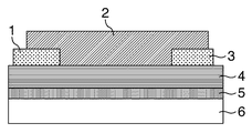
- FIG. 1 is a schematic view showing an embodiment of the field effect transistor of the present invention.
- FIG. 2 is a schematic view of a process for manufacturing one embodiment of the field effect transistor of the present invention.
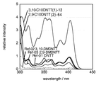
- FIG. 3 is a schematic view of the field effect transistor of the present invention obtained in Comparative Example 1. It is the light absorption spectrum of the chloroform solution of each DNTT.
- the present invention relates to an organic field effect transistor using a specific organic compound as a semiconductor material, and a semiconductor layer is formed by using the compound represented by the formula (1) as a semiconductor material. Therefore, first, the compound of the above formula (1) will be described.
- R 1 and R 2 each represent a hydrogen atom, a C2-C16 alkyl group, or an aryl group.
- R 1 independently represents a C2-C16 alkyl group or an aryl group
- R 2 represents a hydrogen atom or each independently an aryl group
- R 1 is a hydrogen atom
- each R 2 independently represents an aryl group.
- alkyl group for R 1 examples include a linear, branched or cyclic alkyl group, and the carbon number thereof is usually 2 to 16, preferably 4 to 14, and more preferably 6 to 12.
- specific examples of the linear alkyl group include ethyl, n-propyl, n-butyl, n-pentyl, n-hexyl, n-heptyl, n-octyl, n-nonyl, n-decyl, n-undecyl. N-dodecyl, n-tridecyl, n-tetradecyl, n-pentadecyl, n-hexadecyl and the like.
- branched chain alkyl group examples include C3-C16 saturated branched chain alkyl groups such as i-propyl, i-butyl, i-pentyl, i-hexyl, i-decyl and the like.
- cyclic alkyl group examples include C5-C16 cycloalkyl groups such as cyclohexyl, cyclopentyl, adamantyl, norbornyl and the like.
- a saturated alkyl group is preferable to unsaturated, and an unsubstituted one is preferable to one having a substituent.
- a C4-C14 saturated linear alkyl group a C6-C12 saturated linear alkyl group, more preferably an n-hexyl, n-octyl, n-decyl, and n-dodecyl group are more preferable.
- Examples of the aryl group of R 1 and R 2 include a phenyl group, a biphenyl group, a pyrene group, a 2-methylphenyl group, a 3-methylphenyl group, a 4-methylphenyl group, a 4-butylphenyl group, a 4-hexylphenyl group, 4-octylphenyl group, 4-decylphenyl group, xylyl group, mesityl group, cumenyl group, benzyl group, phenylethyl group, ⁇ -methylbenzyl group, triphenylmethyl group, styryl group, cinnamyl group, biphenylyl group, 1- Represents an aromatic hydrocarbon group such as a naphthyl group, a 2-naphthyl group, an anthryl group or a phenanthryl group, or a heterocyclic group such as a 2-thienyl group, and these groups may have a substitu
- R 1 represents a C2-C16 alkyl group or an aryl group
- R 2 represents a hydrogen atom or each independently an aryl group
- R 1 represents a hydrogen atom
- each R 2 independently represents an aryl group
- R 1 and R 2 may be the same or different from each other, but it is more preferable that R 1 and R 2 are independently the same. This means that R 1 is preferably the same on the left and right and R 2 is the same on the left and right, but R 1 and R 2 need not be the same.
- the compound represented by the formula (1) can be synthesized by a method for producing the formula (2) described later.
- the purification method of the compound represented by Formula (1) is not particularly limited, and known methods such as recrystallization, column chromatography, and vacuum sublimation purification can be employed. These methods can be combined as necessary.
- Table 1 shows specific examples of the compound represented by the formula (1).
- n represents normal, i represents iso, s represents secondary, t represents tertiary, and cy represents cyclo.
- Ph represents a phenyl group
- Tolyl represents a tolyl group
- PhPh represents a biphenyl group
- Nap represents a naphthyl group
- 2-thienyl represents a 2-thiophene group.
- the blank represents hydrogen.
- the production method of the compound of the present invention is a novel production method, and this production method is not only a novel compound of the formula (1), but also R 1 is a hydrogen atom, R 2 is an alkyl group ((C2 Known DNTTs such as DNTT which are -C16) alkyl groups, etc.) can also be produced in very high yields.
- the reaction formula of the present invention is as follows. Hereinafter, reaction formulas (4), (5), and (6) will be described in order.
- R 3 represents a substituent, and the substituent is a hydrogen atom, alkyl group, aryl group, ether group, thioether group, ester group, acyl group, amino group, cyano group. , A nitro group and the like, and these groups may have a substituent, and may be the same or different.
- the alkyl group in R 3 is a linear, branched or cyclic C1-C16 alkyl group, and the aryl group has the same meaning as the aryl group of R 1 and R 2 in the compound (1).
- the ether group is an alkoxy group having an alkyl group having 1 to 16 carbon atoms bonded to an oxygen atom, or an aryl group (aryloxy group) bonded to an oxygen atom.
- the thioether group is a thioalkoxy group having an alkyl group having 1 to 16 carbon atoms bonded to a sulfur atom, or an aryl group (arylthio group) bonded to a sulfur atom.
- R 3 is preferably a C1-C16 saturated linear alkyl group and an aryl group having a phenyl, naphthyl, or biphenyl skeleton. More preferably, they are a C4-C14 saturated linear alkyl group, a phenyl group, a 4-methylphenyl group, and a biphenyl group.
- R 4 represents a hydrogen atom; an alkyl group; an aryl group; an alkyl SO 2 group; an aryl SO 2 group; an alkyl group in which one or more hydrogen atoms are substituted with a fluorine atom; A group, an alkyl SO 2 group or an aryl SO 2 group;
- alkyl group has the same meaning as the alkyl group of R 3 .
- Aryl groups are the same meaning as the aryl group of R 1 and R 2.
- Alkyl SO 2 group, the aryl SO 2 group, respectively SO 2 group of the above alkyl group is substituted, is that the SO 2 group in which the aryl group is substituted.
- the alkyl group in which one or more hydrogen atoms are substituted with fluorine atoms is an alkyl group in which at least one hydrogen atom of the alkyl group is substituted with fluorine atoms, and an alkyl group in which all hydrogen atoms are substituted with fluorine atoms (Hereinafter collectively referred to as a fluorinated alkyl group).
- Preferable fluorinated alkyl groups are alkyl groups in which all hydrogen atoms are replaced by fluorine atoms, and examples thereof include trifluoromethyl groups and perfluorohexyl groups (nC 6 F 13 ).
- the aryl group in which one or more hydrogen atoms are substituted with fluorine atoms is an aryl group in which at least one hydrogen atom of the aryl group of the substituent R 3 is substituted with fluorine atoms, and all the hydrogen atoms are substituted with fluorine atoms (Hereinafter collectively referred to as a fluorinated aryl group).
- a fluorinated aryl group a 4-trifluoromethylphenyl group (4-CF 3 C 6 H 5 ), a pentafluorophenyl group (C 6 F 5 ), which is an aryl group in which all hydrogen atoms are replaced with fluorine atoms, are used. Is mentioned.
- An alkyl SO 2 group in which one or more hydrogen atoms are substituted with a fluorine atom is a fluorinated alkyl SO 2 group.
- Preferred fluorinated alkyl SO 2 group wherein all the hydrogen atoms are alkyl SO 2 groups replaced by fluorine atoms, trifluoromethyl SO 2 group, perfluorohexyl an SO 2 group can be mentioned.
- the aryl SO 2 group in which one or more hydrogen atoms are substituted with fluorine atoms is the fluorinated aryl SO 2 group.
- Preferred fluorinated aryl SO 2 group, 4-fluorophenyl SO 2 group, 4-trifluoromethylphenyl SO 2 group, pentafluorophenyl SO 2 groups are all aryl SO 2 group in which a hydrogen atom is replaced with fluorine atom Is mentioned.
- R 4 is preferably a methyl group, a trifluoromethyl group, a perfluorohexyl group, a 4-trifluoromethylphenyl group, a pentafluorophenyl group which is an aryl group in which all hydrogen atoms are replaced by fluorine atoms, or trifluoromethyl SO. 2 groups, perfluorohexyl SO 2 group, 4-trifluoromethylphenyl SO 2 group, and pentafluorophenyl SO 2 group which is an aryl group in which all hydrogen atoms are replaced with fluorine atoms. More preferable R 4 includes a methyl group and a trifluoromethyl SO 2 group.
- reaction formula (4) will be described. Many of the compounds of the following formula (3) as starting materials are available as commercial products, and can also be easily synthesized by the methods shown in the examples.
- R 3 is described as R 31 and R 32 as follows.
- the blank indicates a hydrogen atom.
- reaction formula (4) will be described in detail.
- This reaction is a novel reaction, and it is converted to SMe by using dimethyldisulfide (Me 2 S 2 ) with high selectivity at the 3-position of the compound (3) which is a starting material bonded to the oxygen atom at the 2-position. It is a feature.
- the inventors examined a base (alkyl metal reagent, alkyl earth metal reagent), a reaction solvent, a reaction temperature, and an operation procedure for metalation by hydrogen extraction at the 3-position, A production method has been found in which SMe is converted to dimethyldisulfide with high selectivity at the 3-position of compound (3).
- an alkali metal reagent such as a lithium reagent, a sodium reagent, or a potassium reagent
- an alkyl earth metal reagent such as a magnesium reagent or a calcium reagent.
- methyl lithium, n-butyl lithium, t-butyl lithium, phenyl lithium, methyl magnesium chloride, butyl magnesium chloride, or the like can be used.
- Particularly preferred is the use of butyl lithium, which is a stable and strong base.
- the amount of the base used is desirably 0.5 mol or more and 10 mol or less with respect to 1 mol of the compound (3). You may add a base in the range of the said usage-amount further to the reaction solution which added the compound (3) to the base. By adding the base in two steps as described above, the extraction of the hydrogen atom at the 3-position of the compound (3) may be smooth.
- a basic compound may be added together with the alkyl metal reagent for the purpose of stabilizing the lithium reagent.
- Examples of basic compounds include N, N, N′-trimethylethylenediamine, dimethylamine, diisopropylamine, morpholine and the like.
- the reaction is preferably carried out in an inert gas atmosphere such as an argon atmosphere, a nitrogen substitution, a dry argon atmosphere, or a dry nitrogen stream.
- an inert gas atmosphere such as an argon atmosphere, a nitrogen substitution, a dry argon atmosphere, or a dry nitrogen stream.
- the reaction temperature when reacting the above compound (3) with a base is preferably in the range of ⁇ 100 ° C. to 30 ° C., more preferably ⁇ 80 ° C. to 10 ° C.
- any solvent can be used, but an ether solvent, an aliphatic solvent, or an aromatic solvent is desirable. In addition, it is desirable to use a solvent obtained by drying moisture.
- ether solvents used in the reaction include tetrahydrofuran (THF), diethyl ether, dimethoxyethane, dioxane and the like.
- aliphatic solvent examples include n-pentane, n-hexane, and n-heptane, and examples of the aromatic solvent include toluene and xylene.
- the amount of dimethyl disulfide used in the reaction is desirably 0.5 mol or more and 10 mol or less with respect to 1 mol of the compound (3).
- the purification method is not particularly limited, and a known purification method can be used according to the physical properties of the compound. Specifically, it can be purified by recrystallization, column chromatography or the like.
- R 5 represents an alkyl group.
- the alkyl group include straight-chain or branched-chain alkyl groups, and the carbon number thereof is 1 to 8, preferably 1 to 4, and more preferably 4.
- specific examples of the linear alkyl group include methyl, ethyl, n-propyl, n-butyl, n-pentyl, n-hexyl and the like.
- Specific examples of the branched chain alkyl group include C3-C6 saturated branched chain alkyl groups such as i-propyl, i-butyl, t-butyl, i-pentyl, i-hexyl and the like. Preferably, it is an n-butyl group that is easily available.
- R 3 (R 31 and R 32) are the same meaning as R 3 of Compound (3) (R 31 and R 32).
- compound (6) (compound (6) -01 to compound (6) -71) are shown below, but the present invention is not limited thereto.
- R 3 of the compound (6) is also described as R 31 and R 32 for convenience.
- the compound (5) reacts with the elimination of the oxygen atom at the 2-position of the bimolecular compound (4) having a MeS group at the 3-position, whereby the compound (6) can be produced with high selectivity.
- reaction formula (5) In general, in the reaction of the reaction formula (5), a Pd-based compound is used as a catalyst. However, Pd is easily violated by a sulfur compound and may lose its activity immediately.
- the present inventors have studied the catalyst, reaction solvent, reaction temperature, and operating procedure for effectively desorbing oxygen from the compound (4) and reacting with the compound (5) as described above.
- the production method capable of obtaining compound (6) from 4) with high selectivity and high yield was found.
- R 4 of the compound (4) can be converted to a more optimal substituent and used as necessary when the reaction of the reaction formula (5) is performed. That is, the conversion can be performed in a timely manner as shown in the embodiment.
- the mixing ratio of the compound (4) and the compound (5) when carrying out the reaction of the reaction formula (5) is that 1.8 mol to 2.5 mol of the compound (4) with respect to 1 mol of the compound (5). preferable. More preferably, it is carried out at 1.95 mol to 2.10 mol, and even more preferably at 1.95 mol to 2.05 mol.
- the compound (4) and the compound (5) are first reacted at a ratio of about 1: 1, and then a compound (4) having another substituent different from the compound (4) added first is added.
- an asymmetric intermediate (6) can also be synthesized.
- any Pd or Ni-based catalyst can be used, but at least one catalyst is tri-tert-butylphosphine, triadamantylphosphine, 1,3-bis ( 2,4,6-trimethylphenyl) imidazolidinium chloride, 1,3-bis (2,6-diisopropylphenyl) imidazolidinium chloride, 1,3-diadamantylimidazolidinium chloride, or a mixture thereof; metal Pd , Pd / C (with or without water), bis (triphenylphosphino) palladium dichloride (Pd (PPh 3 ) 2 Cl 2 ), palladium (II) acetate (Pd (OAc) 2 ), tetrakis (triphenylphosphine) palladium (Pd (PPh 3 ) 4 ), tetrakis (tripheny Ruphosphine) nickel (Ni (PPh 3 ) 4 ), nickel
- the amount of catalyst used is preferably 0.001 mol or more and 0.5 mol or less with respect to 1 mol of the compound (4). You may add a catalyst in the range of the said usage-amount to the reaction solution which added the compound (4), the compound (5), and the catalyst. When the catalyst is poisoned by sulfur or the like and deactivated, adding the catalyst in two or more stages in this way is effective because the reduction in the reaction rate may be suppressed.
- the reaction temperature for reacting compound (4) with compound (5) is usually from ⁇ 10 ° C. to 200 ° C. More preferably, it is 40 ° C to 180 ° C, and still more preferably 80 ° C to 150 ° C.
- the reaction is preferably carried out in an inert gas atmosphere such as an argon atmosphere, a nitrogen substitution, a dry argon atmosphere, or a dry nitrogen stream.
- an inert gas atmosphere such as an argon atmosphere, a nitrogen substitution, a dry argon atmosphere, or a dry nitrogen stream.
- a solvent may or may not be used. Any solvent can be used as long as it is a solvent used in ordinary organic synthesis.
- aromatic compounds such as chlorobenzene, o-dichlorobenzene, bromobenzene, nitrobenzene, toluene, xylene, and saturated aliphatic hydrocarbons such as n-hexane, n-heptane, n-pentane; cyclohexane, cycloheptane, cyclopentane
- Alicyclic hydrocarbons such as n-propyl bromide, n-butyl chloride, n-butyl bromide, dichloromethane, dibromomethane, dichloropropane, dibromopropane, dichloroethane, dibromoethane, dichloropropane, dibromopropane, dichlorobutane, chloroform, Saturated aliphatic halogen
- At least one high boiling point solvent having a boiling point of 100 ° C. or higher as the reaction solvent because the reaction rate is greatly improved and the selectivity of the reaction is further increased.
- High boiling point solvents having a boiling point of 100 ° C. or higher are amides (N-methyl-2-pyrrolidone (hereinafter referred to as NMP), N, N-dimethylformamide (hereinafter abbreviated as DMF), N, N-dimethylacetamide (hereinafter referred to as DMAc). )); Glycols (ethylene glycol, propylene glycol, polyethylene glycol); and sulfoxides (dimethyl sulfoxide (hereinafter abbreviated as DMSO)) are preferred, and N-methyl-2-pyrrolidone, N, N-dimethyl are more preferred.
- NMP N-methyl-2-pyrrolidone
- DMF N, N-dimethylformamide
- DMAc N-dimethylacetamide
- DMSO sulfoxides
- the purification method is not particularly limited, and a known purification method can be used according to the physical properties of the compound (6). Specifically, it can be purified by recrystallization, column chromatography or the like.
- reaction formula (6) will be described.
- the compounds (2) -01 to 53 are the same compounds as the compounds (1) -01 to 53.
- the compounds (1) -01 to 53 are used.
- the compound of the present invention can be obtained in high yield from compound (6). (2) can be given.
- R 3 is described as R 31 and R 32 for convenience.
- a field effect transistor (Field effect transistor, hereinafter abbreviated as FET) of the present invention has two electrodes (a source electrode and a drain electrode) in contact with a semiconductor, and a current flowing between the electrodes is connected to a gate electrode. It is controlled by a voltage applied to another electrode called.
- FET Field effect transistor
- a structure in which a gate electrode is insulated by an insulating film is often used for a field effect transistor.
- An insulating film using a metal oxide film is called a MOS structure.
- a gate electrode is formed via a Schottky barrier, that is, an MES structure, but in the case of an FET using an organic semiconductor material, an MIS structure is often used.
- FIG. 1 shows some embodiments of the field effect transistor (element) of the present invention.
- 1 is a source electrode
- 2 is a semiconductor layer
- 3 is a drain electrode
- 4 is an insulator layer
- 5 is a gate electrode
- 6 is a substrate.
- positioning of each layer and an electrode can be suitably selected according to the use of an element.
- a to D are called lateral FETs because a current flows in a direction parallel to the substrate.
- A is called a bottom contact structure, and B is called a top contact structure.
- C is a structure often used for fabricating an organic single crystal FET.
- a source and drain electrodes and an insulator layer are provided on a semiconductor, and a gate electrode is further formed thereon.
- D has a structure called a top & bottom contact type transistor.
- E is a schematic diagram of an FET having a vertical structure, that is, a static induction transistor (SIT).
- SIT static induction transistor
- a large amount of carriers can move at a time because the current flow spreads in a plane.
- the source electrode and the drain electrode are arranged vertically, the distance between the electrodes can be reduced, so that the response is fast. Therefore, it can be preferably applied to uses such as flowing a large current or performing high-speed switching.
- FIG. 1E does not show a substrate, but in the normal case, a substrate is provided outside the source and drain electrodes represented by 1 and 3 in FIG. 1E.
- the substrate 6 needs to be able to hold each layer formed thereon without peeling off.
- an insulating material such as a resin plate, film, paper, glass, quartz, or ceramic; an insulating layer formed by coating or the like on a conductive substrate such as metal or alloy; resin and inorganic material, etc. Materials composed of various combinations can be used.
- the resin film that can be used include polyethylene terephthalate, polyethylene naphthalate, polyethersulfone, polyamide, polyimide, polycarbonate, cellulose triacetate, polyetherimide, and the like.
- the element can have flexibility, is flexible and lightweight, and improves practicality.
- the thickness of the substrate is usually 1 ⁇ m to 10 mm, preferably 5 ⁇ m to 5 mm.
- a conductive material is used for the source electrode 1, the drain electrode 3, and the gate electrode 5.
- metals such as platinum, gold, silver, aluminum, chromium, tungsten, tantalum, nickel, cobalt, copper, iron, lead, tin, titanium, indium, palladium, molybdenum, magnesium, calcium, barium, lithium, potassium, sodium, etc.
- conductive oxides such as InO2, ZnO2, SnO2, and ITO
- conductive polymer compounds such as polyaniline, polypyrrole, polythiophene, polyacetylene, polyparaphenylene, vinylene, and polydiacetylene; silicon, germanium, and gallium arsenide And the like; carbon materials such as carbon black, fullerene, carbon nanotube, graphite, etc. can be used.
- the conductive polymer compound or the semiconductor may be doped.
- the dopant examples include inorganic acids such as hydrochloric acid and sulfuric acid; organic acids having an acidic functional group such as sulfonic acid; Lewis acids such as PF5, AsF5 and FeCl3; halogen atoms such as iodine; lithium, sodium and potassium And the like, and the like. Boron, phosphorus, arsenic and the like are also frequently used as dopants for inorganic semiconductors such as silicon.
- a conductive composite material in which carbon black, metal particles, or the like is dispersed in the above dopant is also used.
- the source and drain electrodes are in direct contact with the semiconductor material and serve to inject charges such as electrons and holes into the semiconductor.
- the semiconductor characteristics are improved by inserting an injection improving layer made of a material such as molybdenum oxide or tungsten oxide, doping the metal electrode, or modifying the surface with a monomolecular film. It is also possible.
- the distance (channel length) between the source and drain electrodes is an important factor that determines the characteristics of the device.
- the channel length is usually 0.1 to 300 ⁇ m, preferably 0.5 to 100 ⁇ m. If the channel length is short, the amount of current that can be extracted increases.
- the width (channel width) between the source and drain electrodes is usually 10 to 5000 ⁇ m, preferably 100 to 2000 ⁇ m. In addition, this channel width can be made longer by forming the electrode structure into a comb structure, etc., and the channel width can be set to an appropriate length depending on the required amount of current and the structure of the element. do it.
- Each structure (shape) of the source electrode and the drain electrode will be described.
- the structure of the source and drain electrodes may be the same or different. When it has a bottom contact structure, it is generally preferable to form each electrode using a lithography method and form it in a rectangular parallelepiped.
- the length of the electrode may be the same as the channel width.
- the width of the electrode is usually 0.1 to 1000 ⁇ m, preferably 0.5 to 100 ⁇ m.
- the thickness of the electrode is usually 0.1 to 1000 nm, preferably 1 to 500 nm, more preferably 5 to 200 nm.
- a wiring is connected to each of the electrodes 1, 3, and 5, and the wiring is also made of the same material as the electrode.
- the insulating layer 4 is made of an insulating material.
- polymers such as polyparaxylylene, polyacrylate, polymethyl methacrylate, polystyrene, polyvinylphenol, polyamide, polyimide, polycarbonate, polyester, polyvinyl alcohol, polyvinyl acetate, polyurethane, polysulfone, epoxy resin, phenol resin, fluorine resin, etc.
- the film thickness of the insulator layer 4 varies depending on the material, but is usually 0.1 nm to 100 ⁇ m, preferably 0.5 nm to 50 ⁇ m, more preferably 1 nm to 10 ⁇ m.
- an organic thin film composed of one or more of the heterocyclic compounds represented by the compound (1) is used.
- the compound in the organic thin film may be a mixture, but the organic thin film preferably contains compound (1) in an amount of usually 50% by mass or more, preferably 80% by mass or more, and more preferably 95% by mass or more.
- an organic thin film using at least one kind of heterocyclic compound of compound (1) as a semiconductor material is used.
- the semiconductor material a plurality of heterocyclic rings of compound (1) are substantially used. It is preferred to use a single heterocyclic compound as the semiconductor material rather than a mixture of formula compounds.
- the semiconductor layer may also be composed of a plurality of organic thin film layers, but it is more preferably a single layer structure.
- the thickness of the semiconductor layer 2 is preferably as thin as possible without losing necessary functions. In lateral field effect transistors as shown in A, B, and D, the device characteristics do not depend on the film thickness if the film thickness exceeds a predetermined value, while the leakage current may increase as the film thickness increases. This is because there are many.
- the film thickness of the semiconductor layer for exhibiting the necessary function is usually 1 nm to 10 ⁇ m, preferably 5 nm to 5 ⁇ m, more preferably 10 nm to 3 ⁇ m.
- other layers can be provided as necessary between the substrate and the insulating film layer, between the insulating film layer and the semiconductor layer, or on the outer surface of the element.
- a protective layer is formed directly on the semiconductor layer or via another layer, the influence of outside air such as humidity can be reduced, and the ON / OFF ratio of the element can be increased.
- the material of the protective layer is not particularly limited.
- films made of various resins such as acrylic resin such as epoxy resin and polymethyl methacrylate, polyurethane, polyimide, polyvinyl alcohol, fluororesin, polyolefin, etc .; silicon oxide, aluminum oxide, nitriding
- An inorganic oxide film such as silicon; a film made of a dielectric such as a nitride film; and the like are preferably used.
- a resin (polymer) having a low oxygen and moisture permeability and a low water absorption rate is preferable.
- protective materials developed for organic EL displays can also be used.
- the thickness of the protective layer can be selected according to the purpose, but is usually 100 nm to 1 mm.
- the characteristics of organic semiconductor materials may vary depending on the state of the film, such as molecular orientation.
- the degree of hydrophilicity / hydrophobicity of the substrate surface the film quality of the film formed thereon can be improved.
- the characteristics of organic semiconductor materials can vary greatly depending on the state of the film, such as molecular orientation. Therefore, the surface treatment on the substrate or the like controls the molecular orientation at the interface between the substrate and the semiconductor layer to be formed thereafter, and reduces the trap sites on the substrate and the insulator layer.
- the trap site refers to a functional group such as a hydroxyl group present in an untreated substrate. When such a functional group is present, electrons are attracted to the functional group, and as a result, carrier mobility is lowered. . Therefore, reducing trap sites is often effective for improving characteristics such as carrier mobility.
- Examples of the substrate treatment for improving the characteristics as described above include hydrophobization treatment with hexamethyldisilazane, cyclohexene, octyltrichlorosilane, octadecyltrichlorosilane, etc .; acid treatment with hydrochloric acid, sulfuric acid, acetic acid, etc .; sodium hydroxide, Alkaline treatment with potassium hydroxide, calcium hydroxide, ammonia, etc .; ozone treatment; fluorination treatment; plasma treatment with oxygen or argon; Langmuir / Blodgett film formation treatment; other insulator or semiconductor thin film formation treatment; Examples include mechanical treatment; electrical treatment such as corona discharge; and rubbing treatment using fibers and the like.
- the field effect transistor using the compound of the present invention is characterized in that the influence of the material on the substrate or the insulator layer is small. This eliminates the need for more costly processing and surface condition adjustment, and allows a wider range of materials to be used, leading to versatility and cost reduction.
- a vacuum deposition method for example, a vacuum deposition method, a sputtering method, a coating method, a printing method, a sol-gel method, or the like can be appropriately employed as a method for providing each layer such as an insulating film layer and a semiconductor layer.
- the field effect transistor of the present invention is manufactured by providing various layers and electrodes necessary on the substrate 6 (see FIG. 2A).
- the substrate those described above can be used. It is also possible to perform the above-described surface treatment or the like on this substrate. If the thickness of the board
- substrate 6 is a range which does not prevent a required function, the thinner one is preferable. Although it varies depending on the material, it is usually 1 ⁇ m to 10 mm, preferably 5 ⁇ m to 5 mm. Further, if necessary, the substrate may have an electrode function.
- a gate electrode 5 is formed on the substrate 6 (see FIG. 2B).
- the electrode material described above is used as the electrode material.
- various methods can be used. For example, a vacuum deposition method, a sputtering method, a coating method, a thermal transfer method, a printing method, a sol-gel method, and the like are employed. It is preferable to perform patterning as necessary so as to obtain a desired shape during or after film formation.
- Various methods can be used as the patterning method, and examples thereof include a photolithography method combining photoresist patterning and etching.
- the film thickness of the gate electrode 5 varies depending on the material, but is usually 0.1 nm to 10 ⁇ m, preferably 0.5 nm to 5 ⁇ m, and more preferably 1 nm to 1 ⁇ m. Moreover, when it serves as a gate electrode and a board
- insulator layer 4 is formed over the gate electrode 5 (see FIG. 2 (3)).
- the insulator material those described above are used.
- Various methods can be used to form the insulator layer 4. For example, spin coating, spray coating, dip coating, casting, bar coating, blade coating and other coating methods, screen printing, offset printing, inkjet printing methods, vacuum deposition, molecular beam epitaxial growth, ion cluster beam method, ion plating Examples thereof include dry process methods such as a coating method, a sputtering method, an atmospheric pressure plasma method, and a CVD method.
- a sol-gel method alumite on aluminum, a method of forming an oxide film on a metal such as silicon dioxide on silicon, and the like are employed.
- a predetermined amount is provided on the insulator layer.
- the surface treatment can also be performed.
- the same surface treatment as that of the substrate can be used.
- the thickness of the insulator layer 4 is preferably as thin as possible without impairing its function. Usually, the thickness is 0.1 nm to 100 ⁇ m, preferably 0.5 nm to 50 ⁇ m, more preferably 5 nm to 10 ⁇ m.
- the formation method of the source electrode 1 and the drain electrode 3 can be formed according to the manufacturing method of the gate electrode 5 (see FIG. 2 (4)).
- an organic thin film composed of one or more heterocyclic compounds represented by the compound (1) is formed as a semiconductor layer.
- the semiconductor material an organic material containing a total amount of one or more kinds of heterocyclic compounds of compound (1) is usually 50% by mass or more.
- Various methods can be used for forming the semiconductor layer. Formation method in a vacuum process such as sputtering method, CVD method, molecular beam epitaxial growth method, vacuum deposition method; coating method such as dip coating method, die coater method, roll coater method, bar coater method, spin coating method, ink jet method, It is roughly classified into solution forming methods such as screen printing, offset printing, and microcontact printing.
- the method of forming the organic thin film formed by the vacuum process as a semiconductor layer is the method.
- the vacuum evaporation method is more preferable. It is possible to form a film by a solution process, and it is possible to adopt a printing method at a low cost.
- a method for obtaining an organic thin film by depositing an organic material by a vacuum process will be described.
- the organic material is heated in a crucible or a metal boat under vacuum, and the evaporated organic material is attached (evaporated) to a substrate (exposed portions of the insulator layer, the source electrode and the drain electrode), that is, A vacuum deposition method is preferably employed.
- the degree of vacuum is usually 1.0 ⁇ 10 ⁇ 1 Pa or less, preferably 1.0 ⁇ 10 ⁇ 3 Pa or less.
- the characteristics of the organic semiconductor film, and hence the field effect transistor may vary depending on the substrate temperature during vapor deposition, it is necessary to carefully select the substrate temperature.
- the substrate temperature during vapor deposition is usually 0 to 200 ° C., preferably 10 to 150 ° C., more preferably 15 to 120 ° C., and further preferably 25 to 100 ° C.
- the deposition rate is usually 0.001 nm / second to 10 nm / second, preferably 0.01 nm / second to 1 nm / second.
- the thickness of the organic semiconductor layer made of an organic material is usually 1 nm to 10 ⁇ m, preferably 5 nm to 5 ⁇ m, more preferably 10 nm to 3 ⁇ m.
- the sputtering method in which ions such as accelerated argon collide with the material target to knock out the material atoms and adhere to the substrate. May be used.
- the semiconductor material in the present invention is an organic compound and is a relatively low molecular compound, such a vacuum process can be preferably used. Although such a vacuum process requires somewhat expensive equipment, there is an advantage that a uniform film can be easily obtained with good film formability.
- a solution process that is, a coating method can also be suitably used.
- the method will be described.
- the semiconductor material containing the heterocyclic compound of the compound (1) in the present invention can be dissolved or dispersed in an organic solvent, and practical semiconductor characteristics can be obtained by a solution process.
- the manufacturing method by the coating method is advantageous in that a large-area field effect transistor can be realized at a low cost because it is not necessary to make the manufacturing environment vacuum or high temperature.
- an ink for preparing a semiconductor device is prepared by dissolving or dispersing a heterocyclic compound of compound (1) in a solvent.
- the solvent at this time is not particularly limited as long as the compound can be dissolved or dispersed and formed on the substrate.
- the solvent is preferably an organic solvent, specifically, a halogeno hydrocarbon solvent such as chloroform, methylene chloride, or dichloroethane; an alcohol solvent such as methanol, ethanol, isopropyl alcohol, or butanol; an octafluoropentanol, pentafluoropropanol, or the like.
- Fluorinated alcohol solvents such as ethyl acetate, butyl acetate, ethyl benzoate and diethyl carbonate; toluene, hexylbenzene, xylene, mesitylene, chlorobenzene, dichlorobenzene, methoxybenzene, chloronaphthalene, methylnaphthalene, tetrahydronaphthalene, etc.
- Aromatic hydrocarbon solvents such as acetone, methyl ethyl ketone, methyl isobutyl ketone, cyclopentanone, cyclohexanone; dimethylforma De, dimethyl acetamide, amide solvents such as N- methylpyrrolidone; tetrahydrofuran, ether solvents diisobutyl ether, diphenyl ether, etc.; octane, decane, decalin, and the like can be used hydrocarbon solvents such as cyclohexane. These can be used alone or in combination. It is also possible to mix additives and other semiconductor materials for the purpose of improving the film formability of the semiconductor layer and doping described later.
- additives vary depending on the required functions, such as conductive, semiconducting and insulating high molecular compounds and low molecular compounds, dopants, dispersants, surfactants, leveling agents, and surface tension modifiers. Is mentioned.
- concentration of the total amount of the heterocyclic compound of compound (1) or a mixture thereof in the ink varies depending on the type of solvent and the thickness of the semiconductor layer to be produced, but is usually about 0.001% to 50%, preferably It is about 0.01% to 20%.
- a semiconductor material containing the heterocyclic compound of the compound (1) or the like is dissolved or dispersed in the above solvent, and if necessary, a heat dissolution treatment is performed.
- the obtained solution is filtered using a filter or the like, and solids such as impurities are removed to obtain an ink for manufacturing a semiconductor device.
- an ink is used, the film formability of the semiconductor layer is improved, which is preferable for manufacturing the semiconductor layer.
- the semiconductor element manufacturing ink prepared as described above is applied to the substrate (exposed portions of the insulator layer, the source electrode, and the drain electrode).
- Coating methods include casting, spin coating, dip coating, blade coating, wire bar coating, spray coating, and other coating methods, inkjet printing, screen printing, offset printing, letterpress printing, and other micro contact printing methods.
- the method of soft lithography, etc., or a method combining a plurality of these methods may be employed.
- the Langmuir project method in which the monolayer film of the semiconductor layer produced by dropping the above ink on the water surface is transferred to the substrate and laminated, and two substrates of liquid crystal or melted material are used.
- the film thickness of the organic semiconductor layer produced by this method is preferably thin as long as the function is not impaired. There is a concern that the leakage current increases as the film thickness increases.
- the thickness of the organic semiconductor layer is usually 1 nm to 10 ⁇ m, preferably 5 nm to 5 ⁇ m, more preferably 10 nm to 3 ⁇ m.
- the characteristics of the semiconductor layer thus formed can be further improved by post-processing.
- semiconductor characteristics can be improved and stabilized by heat treatment. This is considered to be due to the fact that the strain in the film caused by the heat treatment is alleviated, pinholes and the like are reduced, and the arrangement and orientation in the film can be controlled.
- this heat treatment is performed by heating the substrate after forming the semiconductor layer.
- the temperature of the heat treatment is not particularly limited, but is usually about room temperature to 200 ° C.
- the heat treatment time at this time is not particularly limited but is usually 1 minute to 24 hours.
- the atmosphere at that time may be air, but may be an inert atmosphere such as nitrogen or argon.
- treatment with oxidizing or reducing gas such as oxygen or hydrogen, oxidizing or reducing liquid, etc. may induce a change in characteristics due to oxidation or reduction. it can. This is often used for the purpose of increasing or decreasing the carrier density in the film, for example.
- the semiconductor layer characteristics can be changed by adding a trace amount of elements, atomic groups, molecules, and polymers to the semiconductor layer.
- elements for example, oxygen, hydrogen, hydrochloric acid, sulfuric acid, sulfonic acid and other acids; Lewis acids such as PF5, AsF5, and FeCl3; halogen atoms such as iodine; metal atoms such as sodium and potassium; and the like can be doped. This can be achieved by bringing these gases into contact with the semiconductor layer, immersing them in a solution, or performing an electrochemical doping process.
- dopings may be added during the synthesis of the semiconductor material, even after the semiconductor layer is not formed, or may be added to the ink in the process of manufacturing the semiconductor layer using the semiconductor element manufacturing ink. It can be added in the process step of forming the precursor thin film disclosed in Patent Document 2.
- a material used for doping is added to the material for forming the semiconductor layer and co-evaporated, or mixed in an ambient atmosphere when the semiconductor layer is formed (in an environment where the doping material is present). A semiconductor layer is produced), and further, ions can be accelerated in a vacuum and collide with the film for doping.
- doping effects include a change in electrical conductivity due to an increase or decrease in carrier density, a change in carrier polarity (p-type or n-type), a change in Fermi level, and the like.
- Such doping is often used particularly in semiconductor elements using inorganic materials such as silicon.
- the protective layer 7 When the protective layer 7 is formed on the organic semiconductor layer, there is an advantage that the influence of outside air can be minimized and the electrical characteristics of the organic field effect transistor can be stabilized (see FIG. 2 (6)).
- the above-mentioned materials are used as the protective layer material.
- the protective layer 7 may have any thickness depending on the purpose, but is usually 100 nm to 1 mm.
- Various methods can be employed to form the protective layer.
- the protective layer is made of a resin, for example, a method of applying a resin solution and then drying to form a resin film; applying or vapor-depositing a resin monomer The method of polymerizing afterwards; etc. can be adopted. Further, a crosslinking treatment may be performed after the film formation.
- the protective layer is made of an inorganic material, for example, a formation method in a vacuum process such as a sputtering method or a vapor deposition method, or a formation method in a solution process such as a sol-gel method can be used.
- a protective layer can be provided between the layers as necessary, in addition to the organic semiconductor layer. These layers may help to stabilize the electrical properties of the organic field effect transistor.
- an organic material is used as a semiconductor material, it can be manufactured at a relatively low temperature process. Accordingly, flexible materials such as plastic plates and plastic films that could not be used under conditions exposed to high temperatures can be used as the substrate. As a result, it is possible to manufacture an element that is light, flexible, and hard to break, and can be used as a switching element for an active matrix of a display.
- the display include a liquid crystal display, a polymer dispersion type liquid crystal display, an electrophoretic display, an EL display, an electrochromic display, a particle rotation type display, and the like.
- the field effect transistor of the present invention can be used as a digital element and an analog element such as a memory circuit element, a signal driver circuit element, and a signal processing circuit element. Further, by combining these, it is possible to produce an IC card or an IC tag. Furthermore, since the field effect transistor of the present invention can change its characteristics by an external stimulus such as a chemical substance, it can be used as an FET sensor.
- the operating characteristics of a field effect transistor are determined by the carrier mobility of a semiconductor layer, conductivity, the capacitance of an insulator layer, the element configuration (distance and width between source and drain electrodes, film thickness of the insulator layer, etc.), etc. .
- a semiconductor material used for the field effect transistor a material having higher carrier mobility when a semiconductor layer is formed is preferable.
- the heterocyclic compound of the compound (1) in the present invention is excellent in film formability. Furthermore, pentacene derivatives are unstable and difficult to handle, such as decomposition in the atmosphere due to moisture contained in the atmosphere, but the heterocyclic compound of the compound (1) of the present invention is used as a semiconductor material.
- a transistor having a semiconductor layer formed of a heterocyclic compound of compound (1) has a low threshold voltage, in actual use, a driving voltage is low and power consumption is lower than a conventional one. This makes it possible to save energy. For example, when a rechargeable battery is used, it is effective for use in a portable display or the like that requires longer driving time. In addition, the consumption of energy is reduced by lowering the threshold voltage, and the barrier of charge injection from the electrode to the semiconductor film is reduced by lowering the threshold voltage, whereby the durability of the semiconductor element and the semiconductor device having the semiconductor element itself It is expected to be effective in improving
- Example 1-1 Synthesis of 2-decanoyl-6-methoxynaphthalene Nitromethane obtained by drying 2-methoxynaphthalene (64 g, 0.41 mol) readily available from a reagent manufacturer with molecular sieve 3A under a nitrogen atmosphere (150 ml) and aluminum chloride (80 g, 0.60 mol) was added in an ice bath. Subsequently, decanoyl chloride (92 ml, 0.45 mol) was added dropwise thereto in an ice bath. After stirring at room temperature for 5 hours, water (100 ml) was added dropwise in an ice bath.
- the reaction solution was extracted with methylene chloride (200 ml ⁇ 4), and the organic layer was washed with water (100 ml ⁇ 3). The organic layer was dried over anhydrous magnesium sulfate and filtered, and then the solvent was distilled off under reduced pressure. The obtained yellow solid was recrystallized from hexane to obtain 2-decanoyl-6-methoxynaphthalene (102 g, 82%) as a white solid.
- Example 1-2 Synthesis of 6-n-decyl-2-hydroxynaphthalene Under a nitrogen atmosphere, 2-decanoyl-6-methoxynaphthalene (9.4 g, 30 mmol) and potassium hydroxide (67 g, 1.2 mol) were dissolved in hydrazine monohydrate (70 ml, 1.4 mol) and diethylene glycol (200 ml). After refluxing for 17 hours, water (36 ml) was added and distilled under a nitrogen stream to distill off excess amounts of hydrazine and water. Further, the mixture was refluxed for 41 hours under a nitrogen atmosphere. Thereafter, hydrochloric acid was slowly added until neutrality while cooling by adding ice to the reaction solution using an ice bath.
- the reaction solution was extracted with ether (100 ml ⁇ 3), and the organic layer was washed with saturated brine (100 ml ⁇ 5). The organic layer was dried over anhydrous magnesium sulfate and filtered, and then the solvent was distilled off under reduced pressure. The obtained brown solid was recrystallized from hexane to obtain 6-decyl-2-hydroxynaphthalene (7.3 g, 90%) as a white solid.
- Example 1-3 Synthesis of 6-n-decyl-2-methoxynaphthalene (Compound (3) -64) Under a nitrogen atmosphere, a solution of 6-n-decyl-2-hydroxynaphthalene (5.68 g, 20 mmol) and 55% NaH (oil dispersion, 880 mg, 20 mmol) in THF (200 ml) was stirred at room temperature for 40 minutes. CH3I (1.48 ml, 24 mmol) was added to the mixture and heated to reflux for 12 hours. Water (20 ml) was added to the mixture at 0 ° C. and washed with brine. The organic layers were combined, dried over MgSO4, and concentrated with an evaporator.
- Example 2 Synthesis of 6-n-decyl-2-methoxynaphthalene (compound (3) -64) by an alternative method N-decylmagnesium bromide in THF in a THF (10 ml) solution of 6-bromo-2-methoxynaphthalene (2.37 g, 10 mmol) and Ni (dppp) Cl2 (271 mg, 0.5 mmol) readily available from the reagent manufacturer A solution (prepared as a solution of n-decyl bromide (2.2 ml, 11 mmol) and Mg (292 mg, 12 mmol) in THF (2 ml)) was added and the mixture was heated to reflux for 19 hours.
- Example 5 Synthesis of 6-phenyl-2-methoxynaphthalene (Compound (3) -31) 6-Bromo-2-methoxy was prepared in the same manner as in the synthesis method of 7-phenyl-2-methoxynaphthalene of Example 4. The desired product, 6-phenyl-2-methoxyquinaphthalene (compound (3) -31), was obtained in 90% yield from naphthalene (easily available from reagent manufacturers) and phenylboric acid.
- 7-Butyn-1-yl-2-methoxynaphthalene was synthesized using romethanesulfonate (30.63 g, 0.10 mol) and butyne gas (Tokyo Chemicals, 100 g, large excess), and column chromatography (silica gel , Developed with a mixture of toluene and hexane) to obtain a pale yellow oily product of 7-butyn-1-yl-2-methoxynaphthalene (18.1 g, yield 56%).
- Example 11 Synthesis of 7-hexyl-2-methoxynaphthalene (Compound (3) -08) 7-Methoxy-2-naphthyltrifluoro was prepared in the same manner as in the synthesis method of 7-decyl-2-methoxynaphthalene of Example 3. 7-Hexin-1-yl-2-methoxynaphthalene was synthesized using l-methanesulfonate (30.63 g, 0.10 mol) and 1-hexyne (10.27 g, 0.125 mol) and column chromatography.
- Example 12 Synthesis of 7-octyl-2-methoxynaphthalene (Compound (3) -10) 7-Methoxy-2-naphthyltrifluoro was prepared in the same manner as in the synthesis method of 7-decyl-2-methoxynaphthalene of Example 3. Synthesis of 7-octin-1-yl-2-methoxynaphthalene was performed using romethanesulfonate (30.63 g, 0.10 mol) and 1-octyne (13.78 g, 0.125 mol), and column chromatography was performed.
- Example 13 Synthesis of 7-dodecyl-2-methoxynaphthalene (Compound (3) -14)
- 7-methoxy-2-naphthyltrifluor 7-dodecin-1-yl-2-methoxynaphthalene was synthesized using romethanesulfonate (30.63 g, 0.10 mol) and 1-dodecine (20.79 g, 0.125 mol), and column chromatography ( By developing with silica gel and a mixture of toluene and hexane), a pale yellow oily substance of 7-dodecin-1-yl-2-methoxynaphthalene was obtained (32.0 g, quantitative).
- reaction solution was added to saturated aqueous ammonium chloride solution (50 ml) and extracted with ether (30 ml ⁇ 3). The extracts obtained by extraction three times were combined, washed with saturated brine (30 ml ⁇ 3), and dried over MgSO 4. Concentration with an evaporator gave 6-n-decyl-3-methylthio-2-methoxynaphthalene (compound (4) -64) (15.2 g, quantitative) as a yellow oil. The next reaction can be used without further purification.
- Example 15 Synthesis of 7-decyl-3-methylthio-2-methoxynaphthalene (Compound (4) -12)
- 7-decyl-3-methylthio-2-methoxynaphthalene (compound (4) -12) was synthesized from dimethyldisulfide (93% yield, recrystallized from hexane to give yellow crystals).
- Example 16 3-Methylthio-7-phenyl-2-methoxynaphthalene (Compound (4) -22) In the same manner as in Example 14, from 7-phenyl-2-methoxynaphthalene (compound (3) -22) and dimethyl disulfide, 3-methylthio-7-phenyl-2-methoxynaphthalene (compound (4) -22) was obtained in a yield of 77% (recrystallization was performed from hexane to obtain yellow crystals).
- Example 17 Synthesis of 3-methylthio-6-phenyl-2-methoxynaphthalene (Compound (4) -31) In the same manner as in Example 14, 6-phenyl-2-methoxyquinaphthalene (Compound (3) -31) ) And dimethyl disulfide to synthesize 3-methylthio-6-phenyl-2-methoxynaphthalene (compound (4) -31).
- Example 18 Synthesis of 6-tolyl-3-methylthio-2-methoxynaphthalene (Compound (4) -32)
- 6-tolyl-2-methoxynaphthalene (Compound (3) -32, 33.3 g) and dimethyl disulfide gave 6-tolyl-3-methylthio-2-methoxynaphthalene (compound (4) -32, 19.22 g, 49%).
- the next reaction can proceed without further purification.
- EI-MS, m / z 294 (M + )
- Example 19 Synthesis of 7-tolyl-3-methylthio-2-methoxynaphthalene (compound (4) -23)
- 7-tolyl-2-methoxynaphthalene compound (3) -23, (22.2 g, 89 mmol
- EI-MS, m / z 294 (M + )
- Example 21 Synthesis of 7-biphenyl-3-methylthio-2-methoxynaphthalene (Compound (4) -24)
- 7-biphenyl-2-methoxynaphthalene Compound (3) -24, 21.5 g
- 7-biphenyl-3-methylthio-2-methoxynaphthalene was synthesized (compound (4) -24) and recrystallized from toluene to give compound (4) -23 (16.0 g, yield). 65%) was obtained.
- the next reaction can proceed without further purification.
- EI-MS, m / z 356 (M + )
- the substituent of compound (4) can be easily converted to a derivative having another substituent by the following operation.
- Example 27 Synthesis of trans-1,2-bis (7-decyl-3-methylthionaphthalen-2-yl) ethylene (compound (6) -12) In the same manner as in Example 26, 7-decyl-3-methylthio From 2- (trifluoromethanesulfonyloxy) naphthalene (compound (4) -77) and 1,2-bis (tributylstannyl) ethylene (compound (5) -05), trans-1,2-bis (7- Decyl-3-methylthionaphthalen-2-yl) ethylene (compound (6) -12) was obtained.
- Example 28 Synthesis of trans-1,2-bis (3-methylthio-7-phenylnaphth-2-yl) ethylene (Compound (6) -22) 3-methylthio-7-phenyl in the same manner as in Example 26 From -2- (trifluoromethanesulfonyloxy) naphthalene (compound (4) -72) and 1,2-bis (tributylstannyl) ethylene (compound (5) -05), trans-1,2-bis ( 3-Methylthio-7-phenylnaphth-2-yl) ethylene (compound (6) -22) was obtained.
- Example 29 Synthesis of trans-1,2-bis (3-methylthio-6-phenylnaphth-2-yl) ethylene (Compound (6) -31)
- trans-1,2-bis ( 3-methylthio-6-phenylnaphth-2-yl) ethylene was obtained.
- Example 32 Synthesis of trans-1,2-bis (6-biphenyl-3-methylthionaphthalen-2-yl) ethylene (Compound (6) -33)
- 6-biphenyl-3- From methylthio-2-trifluoromethanesulfonyloxynaphthalene (compound (4) -85, 15.8 g) to trans-1,2-bis (6-biphenyl-3-methylthionaphthalen-2-yl) ethylene (compound (6) -33, 8.52 g, yield 76%) as a pale yellow solid.
- EI-MS, m / z 676 (M + )
- Example 46 Synthesis of 3,10-dihexyldinaphtho [2,3-b: 2 ′, 3′-f] thieno [2,3-b] thiophene (Compound (1) -08) Similar to Synthesis Example 14 In the method, trans-1,2-bis (7-hexyl-3-methylthionaphthalen-2-yl) ethylene (compound (6) -08, 6.50 g) is reacted with iodine to produce 3,10-dihexyldinaphtho [2,3-b: 2 ′, 3′-f] thieno [2,3-b] thiophene (compound (1) -08) was obtained as a yellow solid (3.18 g, yield 52%).
- Example 48 Synthesis of 3,10-didodecyldinaphtho [2,3-b: 2 ′, 3′-f] thieno [2,3-b] thiophene (Compound (1) -14) Same as Synthesis Example 14 In this method, trans-1,2-bis (7-dodecyl-3-methylthionaphthalen-2-yl) ethylene (compound (6) -14, 7.80, 11 mmol) is reacted with iodine, and 3,10- Didodecyldinaphtho [2,3-b: 2 ′, 3′-f] thieno [2,3-b] thiophene (compound (1) -14) as a yellow solid (6.26 g, 84% yield) Obtained.
- Example 49 (Production of Top Contact Field Effect Transistor) An n-doped silicon wafer (surface resistance: 0.02 ⁇ ⁇ cm or less) with a 300 nm SiO 2 thermal oxide film treated with octadecyltrichlorosilane was placed in a vacuum deposition apparatus, and the degree of vacuum in the apparatus was 5.0 ⁇ 10 ⁇ It exhausted until it became 3 Pa or less.
- the compound (1) -12, (1) -22 and (1) -31 were deposited on this electrode to a thickness of 50 nm under the condition of a substrate temperature of about 60 ° C. by resistance heating vapor deposition, and the semiconductor layer (2 ) Was formed.
- a shadow mask for electrode preparation is attached to this substrate, placed in a vacuum vapor deposition apparatus, evacuated until the degree of vacuum in the apparatus is 1.0 ⁇ 10 ⁇ 4 Pa or less, and a gold electrode is formed by resistance heating vapor deposition. That is, the source electrode (1) and the drain electrode (3) were deposited to a thickness of 40 nm to obtain a TC (top contact) type field effect transistor of the present invention.
- the thermal oxide film in the n-doped silicon wafer with the thermal oxide film has the function of the insulator layer (4), and the n-doped silicon wafer functions as the substrate (6) and the gate electrode (5).
- the obtained field effect transistor was installed in a prober, and semiconductor characteristics were measured using a semiconductor parameter analyzer 4155C (manufactured by Agilent). For semiconductor characteristics, the gate voltage was scanned from 10 V to -100 V in 20 V steps, the drain voltage was scanned from 10 V to -100 V, and the drain current-drain voltage was measured. As a result, current saturation was observed. From the obtained voltage-current curve, the device showed a p-type semiconductor, and the calculated carrier mobility is shown in Table 7.
- DNTT with a short alkyl chain of Ref-02 and Ref-03 showed only characteristics lower than that of the parent nucleus DNTT (Ref-01).
- the compound (1) of the present invention when used, the characteristics were very high as a field effect transistor using a vapor deposition method using a normal organic substance as a semiconductor. This is a level comparable to the mobility of a field effect transistor using a single crystal, which is not feasible industrially, and a very high mobility was obtained by an industrially suitable vacuum deposition method. Since the field effect transistor of the present application has high performance, it has a very high industrial value such as an expanded range of usable applications.
- Example 52 A saturated solution obtained by dissolving DNTT (compound (2) -64) having a C10 alkyl group at 2,9-position or DNTT (compound (1) -12) having a C10 alkyl group at 3,10-position in chloroform
- the absorption spectrum of is shown in FIG. DNTT having a long-chain alkyl group of C10 shows that when 2,9-C10-DNTT (compound (2) -64) is set to 1, from the relative intensity at the longest absorption wavelength depending on the substitution position, 3,10-C10 -DNTT (compound (1) -12) was 3.9, and it was found that high solubility was exhibited due to the difference in substitution position.
- the solubility at 60 ° C.
- the solubility ratio of DNTT having a short alkyl chain of Ref-02 and Ref-03 is 0.1 and 0.5, respectively, and DNTT (Ref-01, Ref-01, (This compound does not dissolve in most solvents) and does not dissolve in most solvents.
- the compound (1) -12 alkyl-substituted at the 3,10-position is higher in solvent solubility than the compound (2) -64 alkyl-substituted at the 2,9-position, and a solution process is considered. It was found that the compound substituted at the 3,10 position was more excellent. That is, if this excellent solubility is utilized, it becomes possible to produce a field effect transistor by producing a practical ink for producing a semiconductor device and applying the produced ink.
- Example 53 An n-doped silicon wafer (surface resistance: 0.02 ⁇ ⁇ cm or less) with a 300 nm SiO 2 thermal oxide film treated with octadecyltrichlorosilane was placed in a vacuum deposition apparatus, and the degree of vacuum in the apparatus was 5.0 ⁇ 10 ⁇ It exhausted until it became 3 Pa or less.
- the compound (1) -12 and 2- (64) were each deposited to a thickness of 50 nm on this electrode under the condition of a substrate temperature of about 100 ° C. by resistance heating vapor deposition to form a semiconductor layer (2).
- an electrode manufacturing shadow mask (channel width is 1500 ⁇ m) having a channel length L of 40 ⁇ m or 190 ⁇ m is attached to this substrate and placed in a vacuum deposition apparatus, and the degree of vacuum in the apparatus is 1.0 ⁇ 10 ⁇ 4 Pa or less.
- the gold electrode, that is, the source electrode (1) and the drain electrode (3) are vapor-deposited to a thickness of 40 nm by a resistance heating vapor deposition method, and the electric field effect of the present invention which is a TC (top contact) type A transistor was obtained.
- Table 11 The results of measuring these semiconductor characteristics in the same manner as in Example 49 are summarized in Table 11.
- R 1 of the compound (1) of the present invention independently represents a C2-C16 alkyl group
- R 2 is a hydrogen atom.
- the compound (3,10-alkyl-substituted DNTT) is 2,9- It was revealed that the solubility was improved over the alkyl-substituted DNTT.
- at least one of R 1 and R 2 is an aryl group, the heat resistance is greatly improved as compared with DNTT in which it is not substituted, and the characteristics as an organic semiconductor are greatly improved. I found out.
- an organic field effect transistor having excellent characteristics was obtained, and an element exhibiting practical carrier mobility could be produced. As a result, it has become clear that it has adaptability to various device fabrication processes, and has high industrial value such as widening the range of usable processes and applications.
Landscapes
- Chemical & Material Sciences (AREA)
- Organic Chemistry (AREA)
- Engineering & Computer Science (AREA)
- Materials Engineering (AREA)
- Chemical Kinetics & Catalysis (AREA)
- Physics & Mathematics (AREA)
- Spectroscopy & Molecular Physics (AREA)
- Thin Film Transistor (AREA)
- Heterocyclic Carbon Compounds Containing A Hetero Ring Having Oxygen Or Sulfur (AREA)
- Electroluminescent Light Sources (AREA)
- Inks, Pencil-Leads, Or Crayons (AREA)
- Organic Low-Molecular-Weight Compounds And Preparation Thereof (AREA)
Abstract
Priority Applications (7)
| Application Number | Priority Date | Filing Date | Title |
|---|---|---|---|
| CN201280010570.8A CN103391942B (zh) | 2011-02-25 | 2012-02-24 | 新型杂环化合物、制造其中间体的方法及其用途 |
| KR1020147036416A KR101599688B1 (ko) | 2011-02-25 | 2012-02-24 | 신규 헤테로시클릭 화합물, 이를 위한 중간체 제조 방법, 및 이의 용도 |
| JP2013501145A JP5674916B2 (ja) | 2011-02-25 | 2012-02-24 | 新規複素環式化合物及びその中間体の製造方法並びにその用途 |
| US14/000,440 US9018630B2 (en) | 2011-02-25 | 2012-02-24 | Heterocyclic dinaphtho thieno thiophene (DNTT) compounds for use as organic semiconductor thin films in field effect transistors and related methods |
| KR20137022246A KR20140041439A (ko) | 2011-02-25 | 2012-02-24 | 신규 헤테로시클릭 화합물, 이를 위한 중간체 제조 방법, 및 이의 용도 |
| EP12750215.1A EP2679592B1 (fr) | 2011-02-25 | 2012-02-24 | Nouveau composé hétérocyclique, procédé de production d'un intermédiaire de celui-ci, et application associée |
| KR1020157013064A KR101599687B1 (ko) | 2011-02-25 | 2012-02-24 | 신규 헤테로시클릭 화합물, 이를 위한 중간체 제조 방법, 및 이의 용도 |
Applications Claiming Priority (2)
| Application Number | Priority Date | Filing Date | Title |
|---|---|---|---|
| JP2011039403 | 2011-02-25 | ||
| JP2011-039403 | 2011-02-25 |
Publications (1)
| Publication Number | Publication Date |
|---|---|
| WO2012115236A1 true WO2012115236A1 (fr) | 2012-08-30 |
Family
ID=46721008
Family Applications (1)
| Application Number | Title | Priority Date | Filing Date |
|---|---|---|---|
| PCT/JP2012/054604 Ceased WO2012115236A1 (fr) | 2011-02-25 | 2012-02-24 | Nouveau composé hétérocyclique, procédé de production d'un intermédiaire de celui-ci, et application associée |
Country Status (7)
| Country | Link |
|---|---|
| US (1) | US9018630B2 (fr) |
| EP (2) | EP2679592B1 (fr) |
| JP (2) | JP5674916B2 (fr) |
| KR (3) | KR101599688B1 (fr) |
| CN (2) | CN103391942B (fr) |
| TW (1) | TWI525095B (fr) |
| WO (1) | WO2012115236A1 (fr) |
Cited By (9)
| Publication number | Priority date | Publication date | Assignee | Title |
|---|---|---|---|---|
| WO2014136953A1 (fr) * | 2013-03-08 | 2014-09-12 | 国立大学法人神戸大学 | Procédé de fabrication de couche mince de semi-conducteur organique |
| CN104956508A (zh) * | 2013-01-22 | 2015-09-30 | 日本化药株式会社 | 溶液工艺用有机半导体材料和有机半导体设备 |
| WO2015147266A1 (fr) * | 2014-03-28 | 2015-10-01 | 富士フイルム株式会社 | Composition filmogène organique semi-conductrice |
| WO2016088793A1 (fr) * | 2014-12-05 | 2016-06-09 | 日本化薬株式会社 | Composé organique et ses utilisations |
| JP2017143097A (ja) * | 2016-02-08 | 2017-08-17 | 株式会社デンソー | 有機電界効果トランジスタ |
| JP2018026559A (ja) * | 2016-08-03 | 2018-02-15 | 日本化薬株式会社 | 有機光電変換素子、有機光電変換素子用材料及びこれらを用いた有機撮像素子 |
| KR20180043189A (ko) | 2015-08-28 | 2018-04-27 | 디아이씨 가부시끼가이샤 | 유기 화합물, 그 제조법, 그것을 함유하는 유기 반도체 재료 및 그것을 함유하는 유기 트랜지스터 |
| JP2019206506A (ja) * | 2018-05-29 | 2019-12-05 | Dic株式会社 | 芳香族化合物の製造方法 |
| JP2020189793A (ja) * | 2019-05-21 | 2020-11-26 | 国立大学法人東北大学 | 芳香族化合物の製造方法 |
Families Citing this family (14)
| Publication number | Priority date | Publication date | Assignee | Title |
|---|---|---|---|---|
| US9796727B2 (en) | 2009-02-27 | 2017-10-24 | Nippon Kayaku Kabushiki Kaisha | Field effect transistor |
| KR20160011244A (ko) * | 2014-07-14 | 2016-02-01 | 한국과학기술연구원 | 다층 박막의 제조 방법, 이로 인해 형성된 다층 박막, 이를 포함하는 유기 박막 트랜지스터 제조 방법 및 이를 통해 제조된 유기 박막 트랜지스터 |
| WO2016152889A1 (fr) * | 2015-03-23 | 2016-09-29 | 日本化薬株式会社 | Composé organique, matériau organique semi-conducteur, film organique mince et son procédé de production, composition organique semi-conductrice et dispositif organique semi-conducteur |
| WO2017022735A1 (fr) * | 2015-08-04 | 2017-02-09 | 富士フイルム株式会社 | Transistor à couches minces organiques, procédé de fabrication de transistor à couches minces organiques, matériau pour transistor à couches minces organiques, composition pour transistor à couches minces organiques, film semi-conducteur organique, et composé |
| JP6800469B2 (ja) * | 2016-02-29 | 2020-12-16 | 国立研究開発法人産業技術総合研究所 | 有機半導体組成物及びそれらからなる有機薄膜、並びにその用途 |
| US10056563B2 (en) | 2016-04-08 | 2018-08-21 | Samsung Electronics Co., Ltd. | Synthetic method of fused heteroaromatic compound and fused heteroaromatic compound, and intermediate thereof |
| KR102389030B1 (ko) * | 2016-07-19 | 2022-04-20 | 닛뽄 가야쿠 가부시키가이샤 | 촬상 소자용 광전 변환 소자용 재료 및 그것을 포함하는 광전 변환 소자, 촬상 소자 및 광 센서 |
| KR102677490B1 (ko) | 2016-11-08 | 2024-06-20 | 삼성전자주식회사 | 축합 헤테로방향족 화합물의 합성 방법, 축합 헤테로방향족 화합물 및 그 중간체 및 합성 방법 |
| KR102464890B1 (ko) | 2017-10-18 | 2022-11-07 | 삼성전자주식회사 | 축합다환 헤테로방향족 화합물, 유기 박막 및 전자 소자 |
| KR102684640B1 (ko) | 2018-12-03 | 2024-07-11 | 삼성전자주식회사 | 유기 박막, 유기 박막 트랜지스터 및 전자 소자 |
| TWI844726B (zh) * | 2019-09-17 | 2024-06-11 | 日商日本化藥股份有限公司 | 稠合多環芳香族化合物 |
| TW202136272A (zh) * | 2019-12-10 | 2021-10-01 | 日商日本化藥股份有限公司 | 縮合多環芳香族化合物 |
| CN112530989B (zh) * | 2020-12-03 | 2024-04-12 | 南京大学 | 一种超高增益有机放大器及其制备方法 |
| CN112531112B (zh) * | 2020-12-03 | 2024-03-22 | 南京大学 | 一种超高增益有机薄膜晶体管及其制备方法 |
Citations (10)
| Publication number | Priority date | Publication date | Assignee | Title |
|---|---|---|---|---|
| JPH06177380A (ja) | 1992-07-30 | 1994-06-24 | Nec Corp | 電界効果型トランジスタおよびその製造方法 |
| JP2001094107A (ja) | 1999-09-20 | 2001-04-06 | Hitachi Ltd | 有機半導体装置及び液晶表示装置 |
| JP2008010541A (ja) | 2006-06-28 | 2008-01-17 | Konica Minolta Holdings Inc | 有機半導体材料、有機半導体膜、有機薄膜トランジスタ及び有機薄膜トランジスタの製造方法 |
| WO2008047896A1 (fr) * | 2006-10-20 | 2008-04-24 | Nippon Kayaku Kabushiki Kaisha | Transistor à effet de champ |
| WO2008050726A1 (fr) | 2006-10-25 | 2008-05-02 | Hiroshima University | Nouveau composé aromatique à cycle fusionne, son procédé de production et son utilisation |
| KR20080100982A (ko) | 2007-05-15 | 2008-11-21 | 삼성전자주식회사 | 헤테로아센 화합물, 이를 포함하는 유기 박막 및 상기박막을 포함하는 전자 소자 |
| WO2009009790A1 (fr) | 2007-07-12 | 2009-01-15 | President And Fellows Of Harvard College | Dérivés thiéno-thiophène stables à l'air présentant une mobilité de trous élevée |
| JP2009196975A (ja) | 2008-01-23 | 2009-09-03 | Tosoh Corp | ヘテロアセン誘導体、その前駆化合物及びそれらの製造方法 |
| WO2010098372A1 (fr) | 2009-02-27 | 2010-09-02 | 国立大学法人広島大学 | Transistor à effet de champ |
| JP2010258214A (ja) | 2009-04-24 | 2010-11-11 | Ushio Chemix Kk | バンドギャップが広いことを特徴とする有機半導体化合物 |
Family Cites Families (5)
| Publication number | Priority date | Publication date | Assignee | Title |
|---|---|---|---|---|
| EP1138328A1 (fr) | 2000-03-29 | 2001-10-04 | Eli Lilly And Company Limited | Dérivés du naphthalène comme médicaments du SNC |
| DE10229370A1 (de) | 2002-06-29 | 2004-01-15 | Covion Organic Semiconductors Gmbh | 2,1,3-Benzothiadiazole |
| CN101103037B (zh) | 2005-01-19 | 2010-10-13 | 国立大学法人广岛大学 | 新的缩合多环芳族化合物及其应用 |
| JP2009054809A (ja) * | 2007-08-28 | 2009-03-12 | Mitsui Chemicals Inc | 有機トランジスタ |
| JP2009152355A (ja) | 2007-12-20 | 2009-07-09 | Konica Minolta Holdings Inc | 有機薄膜トランジスタの製造方法、及び有機薄膜トランジスタ |
-
2012
- 2012-02-24 US US14/000,440 patent/US9018630B2/en active Active
- 2012-02-24 KR KR1020147036416A patent/KR101599688B1/ko active Active
- 2012-02-24 EP EP12750215.1A patent/EP2679592B1/fr active Active
- 2012-02-24 KR KR20137022246A patent/KR20140041439A/ko not_active Withdrawn
- 2012-02-24 KR KR1020157013064A patent/KR101599687B1/ko active Active
- 2012-02-24 CN CN201280010570.8A patent/CN103391942B/zh active Active
- 2012-02-24 WO PCT/JP2012/054604 patent/WO2012115236A1/fr not_active Ceased
- 2012-02-24 CN CN201410836711.2A patent/CN104650110B/zh active Active
- 2012-02-24 JP JP2013501145A patent/JP5674916B2/ja active Active
- 2012-02-24 EP EP14198144.9A patent/EP2889301B1/fr active Active
- 2012-02-24 TW TW101106275A patent/TWI525095B/zh active
-
2014
- 2014-12-05 JP JP2014246640A patent/JP5901732B2/ja not_active Expired - Fee Related
Patent Citations (10)
| Publication number | Priority date | Publication date | Assignee | Title |
|---|---|---|---|---|
| JPH06177380A (ja) | 1992-07-30 | 1994-06-24 | Nec Corp | 電界効果型トランジスタおよびその製造方法 |
| JP2001094107A (ja) | 1999-09-20 | 2001-04-06 | Hitachi Ltd | 有機半導体装置及び液晶表示装置 |
| JP2008010541A (ja) | 2006-06-28 | 2008-01-17 | Konica Minolta Holdings Inc | 有機半導体材料、有機半導体膜、有機薄膜トランジスタ及び有機薄膜トランジスタの製造方法 |
| WO2008047896A1 (fr) * | 2006-10-20 | 2008-04-24 | Nippon Kayaku Kabushiki Kaisha | Transistor à effet de champ |
| WO2008050726A1 (fr) | 2006-10-25 | 2008-05-02 | Hiroshima University | Nouveau composé aromatique à cycle fusionne, son procédé de production et son utilisation |
| KR20080100982A (ko) | 2007-05-15 | 2008-11-21 | 삼성전자주식회사 | 헤테로아센 화합물, 이를 포함하는 유기 박막 및 상기박막을 포함하는 전자 소자 |
| WO2009009790A1 (fr) | 2007-07-12 | 2009-01-15 | President And Fellows Of Harvard College | Dérivés thiéno-thiophène stables à l'air présentant une mobilité de trous élevée |
| JP2009196975A (ja) | 2008-01-23 | 2009-09-03 | Tosoh Corp | ヘテロアセン誘導体、その前駆化合物及びそれらの製造方法 |
| WO2010098372A1 (fr) | 2009-02-27 | 2010-09-02 | 国立大学法人広島大学 | Transistor à effet de champ |
| JP2010258214A (ja) | 2009-04-24 | 2010-11-11 | Ushio Chemix Kk | バンドギャップが広いことを特徴とする有機半導体化合物 |
Non-Patent Citations (4)
| Title |
|---|
| AGGARWAL,V.K. ET AL.: "Developments in the Simmons-Smith-mediated epoxidation reaction", EUROPEAN JOURNAL OF ORGANIC CHEMISTRY, no. 2, 2002, pages 319 - 326, XP055122138 * |
| HAACK, R. A., ET AL.: "Palladium(0) catalyzed coupling of trans-1,2-Bis(tri-n-butylstannyl) ethylene with aromatic halides: A convenient synthesis of substituted trans-§-bromostyrenes.", TETRAHEDRON LETTERS, vol. 29, no. 23, 1988, pages 2783 - 2786, XP055122130 * |
| J. AM. CHEM. SOC., vol. 129, 2007, pages 2224 - 2225 |
| See also references of EP2679592A4 |
Cited By (17)
| Publication number | Priority date | Publication date | Assignee | Title |
|---|---|---|---|---|
| CN104956508A (zh) * | 2013-01-22 | 2015-09-30 | 日本化药株式会社 | 溶液工艺用有机半导体材料和有机半导体设备 |
| JPWO2014115749A1 (ja) * | 2013-01-22 | 2017-01-26 | 日本化薬株式会社 | 溶液プロセス用有機半導体材料及び有機半導体デバイス |
| CN104956508B (zh) * | 2013-01-22 | 2017-07-21 | 日本化药株式会社 | 溶液工艺用有机半导体材料和有机半导体设备 |
| JPWO2014136953A1 (ja) * | 2013-03-08 | 2017-02-16 | 国立大学法人神戸大学 | 有機半導体薄膜の作製方法 |
| WO2014136953A1 (fr) * | 2013-03-08 | 2014-09-12 | 国立大学法人神戸大学 | Procédé de fabrication de couche mince de semi-conducteur organique |
| WO2015147266A1 (fr) * | 2014-03-28 | 2015-10-01 | 富士フイルム株式会社 | Composition filmogène organique semi-conductrice |
| JP2015192116A (ja) * | 2014-03-28 | 2015-11-02 | 富士フイルム株式会社 | 有機半導体膜形成用組成物 |
| WO2016088793A1 (fr) * | 2014-12-05 | 2016-06-09 | 日本化薬株式会社 | Composé organique et ses utilisations |
| JPWO2016088793A1 (ja) * | 2014-12-05 | 2017-10-19 | 日本化薬株式会社 | 有機化合物及びその用途 |
| KR20180043189A (ko) | 2015-08-28 | 2018-04-27 | 디아이씨 가부시끼가이샤 | 유기 화합물, 그 제조법, 그것을 함유하는 유기 반도체 재료 및 그것을 함유하는 유기 트랜지스터 |
| US10516115B2 (en) | 2015-08-28 | 2019-12-24 | Dic Corporation | Organic compound, method for preparing same, organic semiconductor material containing same, and organic transistor containing same |
| JP2017143097A (ja) * | 2016-02-08 | 2017-08-17 | 株式会社デンソー | 有機電界効果トランジスタ |
| JP2018026559A (ja) * | 2016-08-03 | 2018-02-15 | 日本化薬株式会社 | 有機光電変換素子、有機光電変換素子用材料及びこれらを用いた有機撮像素子 |
| JP2019206506A (ja) * | 2018-05-29 | 2019-12-05 | Dic株式会社 | 芳香族化合物の製造方法 |
| JP7047608B2 (ja) | 2018-05-29 | 2022-04-05 | Dic株式会社 | 芳香族化合物の製造方法 |
| JP2020189793A (ja) * | 2019-05-21 | 2020-11-26 | 国立大学法人東北大学 | 芳香族化合物の製造方法 |
| JP7241346B2 (ja) | 2019-05-21 | 2023-03-17 | 国立大学法人東北大学 | 芳香族化合物の製造方法 |
Also Published As
| Publication number | Publication date |
|---|---|
| KR101599687B1 (ko) | 2016-03-07 |
| CN103391942B (zh) | 2015-11-25 |
| JP2015110571A (ja) | 2015-06-18 |
| CN104650110A (zh) | 2015-05-27 |
| JPWO2012115236A1 (ja) | 2014-07-07 |
| US9018630B2 (en) | 2015-04-28 |
| KR20150061035A (ko) | 2015-06-03 |
| KR20140041439A (ko) | 2014-04-04 |
| CN104650110B (zh) | 2017-04-12 |
| JP5901732B2 (ja) | 2016-04-13 |
| EP2679592B1 (fr) | 2018-10-03 |
| EP2889301A1 (fr) | 2015-07-01 |
| CN103391942A (zh) | 2013-11-13 |
| JP5674916B2 (ja) | 2015-02-25 |
| TW201247677A (en) | 2012-12-01 |
| EP2679592A1 (fr) | 2014-01-01 |
| KR101599688B1 (ko) | 2016-03-07 |
| KR20150013906A (ko) | 2015-02-05 |
| EP2679592A4 (fr) | 2014-07-16 |
| US20130330876A1 (en) | 2013-12-12 |
| TWI525095B (zh) | 2016-03-11 |
| EP2889301B1 (fr) | 2017-10-25 |
Similar Documents
| Publication | Publication Date | Title |
|---|---|---|
| JP5901732B2 (ja) | 新規複素環式化合物及びその中間体の製造方法並びにその用途 | |
| KR101556095B1 (ko) | 신규의 헤테로고리 화합물 및 그 이용 | |
| CN101529609B (zh) | 场效应晶体管 | |
| JP5840197B2 (ja) | 有機電界効果トランジスタ及び有機半導体材料 | |
| JP5728990B2 (ja) | ジカルコゲノベンゾジピロール化合物、該化合物の製造方法、該化合物を含む薄膜及び該薄膜を含む有機半導体デバイス | |
| WO2010098372A1 (fr) | Transistor à effet de champ | |
| JP2010043038A (ja) | ラダー型化合物及び有機半導体材料 | |
| KR20110065511A (ko) | 신규 화합물 및 유기 반도체 재료 | |
| JPWO2012115218A1 (ja) | ジアントラ[2,3−b:2’,3’−f]チエノ[3,2−b]チオフェンの製造方法並びにその用途 | |
| JP5160078B2 (ja) | 電界効果トランジスタ | |
| JP2015199716A (ja) | 多環縮環化合物、有機半導体材料、有機半導体デバイス及び有機トランジスタ | |
| JP2014110347A (ja) | 有機半導体層形成用材料 | |
| JP2014139982A (ja) | 有機半導体層及び有機薄膜トランジスタ | |
| WO2012165612A1 (fr) | Matériau semi-conducteur organique et dispositif électronique organique | |
| JP7521742B2 (ja) | 有機トランジスタ材料及び有機トランジスタ | |
| JP2012184196A (ja) | 含ピロールヘテロアセン化合物、該化合物の製造方法、該化合物を含む薄膜及び該薄膜を含む有機半導体デバイス | |
| JP6420143B2 (ja) | 末端にチオフェンを有する屈曲型のチエノチオフェン骨格を特徴とする有機半導体材料。 | |
| JP6526585B2 (ja) | 縮合多環芳香族化合物及びその用途 | |
| WO2012111533A1 (fr) | Composé pour transistor organique |
Legal Events
| Date | Code | Title | Description |
|---|---|---|---|
| 121 | Ep: the epo has been informed by wipo that ep was designated in this application |
Ref document number: 12750215 Country of ref document: EP Kind code of ref document: A1 |
|
| ENP | Entry into the national phase |
Ref document number: 2013501145 Country of ref document: JP Kind code of ref document: A |
|
| WWE | Wipo information: entry into national phase |
Ref document number: 14000440 Country of ref document: US |
|
| WWE | Wipo information: entry into national phase |
Ref document number: 2012750215 Country of ref document: EP |
|
| ENP | Entry into the national phase |
Ref document number: 20137022246 Country of ref document: KR Kind code of ref document: A |
|
| NENP | Non-entry into the national phase |
Ref country code: DE |