WO2012117784A1 - 電流センサ - Google Patents
電流センサ Download PDFInfo
- Publication number
- WO2012117784A1 WO2012117784A1 PCT/JP2012/051846 JP2012051846W WO2012117784A1 WO 2012117784 A1 WO2012117784 A1 WO 2012117784A1 JP 2012051846 W JP2012051846 W JP 2012051846W WO 2012117784 A1 WO2012117784 A1 WO 2012117784A1
- Authority
- WO
- WIPO (PCT)
- Prior art keywords
- pair
- magnetoresistive
- elements
- conductor
- current sensor
- Prior art date
- Legal status (The legal status is an assumption and is not a legal conclusion. Google has not performed a legal analysis and makes no representation as to the accuracy of the status listed.)
- Ceased
Links
Images

Classifications
-
- G—PHYSICS
- G01—MEASURING; TESTING
- G01R—MEASURING ELECTRIC VARIABLES; MEASURING MAGNETIC VARIABLES
- G01R33/00—Arrangements or instruments for measuring magnetic variables
- G01R33/02—Measuring direction or magnitude of magnetic fields or magnetic flux
- G01R33/06—Measuring direction or magnitude of magnetic fields or magnetic flux using galvano-magnetic devices
- G01R33/09—Magnetoresistive devices
- G01R33/093—Magnetoresistive devices using multilayer structures, e.g. giant magnetoresistance sensors
-
- B—PERFORMING OPERATIONS; TRANSPORTING
- B82—NANOTECHNOLOGY
- B82Y—SPECIFIC USES OR APPLICATIONS OF NANOSTRUCTURES; MEASUREMENT OR ANALYSIS OF NANOSTRUCTURES; MANUFACTURE OR TREATMENT OF NANOSTRUCTURES
- B82Y25/00—Nanomagnetism, e.g. magnetoimpedance, anisotropic magnetoresistance, giant magnetoresistance or tunneling magnetoresistance
-
- G—PHYSICS
- G01—MEASURING; TESTING
- G01R—MEASURING ELECTRIC VARIABLES; MEASURING MAGNETIC VARIABLES
- G01R15/00—Details of measuring arrangements of the types provided for in groups G01R17/00 - G01R29/00, G01R33/00 - G01R33/26 or G01R35/00
- G01R15/14—Adaptations providing voltage or current isolation, e.g. for high-voltage or high-current networks
- G01R15/20—Adaptations providing voltage or current isolation, e.g. for high-voltage or high-current networks using galvano-magnetic devices, e.g. Hall-effect devices, i.e. measuring a magnetic field via the interaction between a current and a magnetic field, e.g. magneto resistive or Hall effect devices
- G01R15/205—Adaptations providing voltage or current isolation, e.g. for high-voltage or high-current networks using galvano-magnetic devices, e.g. Hall-effect devices, i.e. measuring a magnetic field via the interaction between a current and a magnetic field, e.g. magneto resistive or Hall effect devices using magneto-resistance devices, e.g. field plates
-
- H—ELECTRICITY
- H10—SEMICONDUCTOR DEVICES; ELECTRIC SOLID-STATE DEVICES NOT OTHERWISE PROVIDED FOR
- H10N—ELECTRIC SOLID-STATE DEVICES NOT OTHERWISE PROVIDED FOR
- H10N50/00—Galvanomagnetic devices
- H10N50/10—Magnetoresistive devices
Definitions
- the present invention relates to a current sensor that measures the magnitude of a current, for example, a current sensor that includes a magnetoresistive element (TMR element, GMR element).
- TMR element magnetoresistive element
- the current sensor described in Patent Document 1 includes a Wheatstone bridge circuit composed of four magnetoresistive elements.
- the current to be measured is measured by the output signals from two pairs of magnetoresistive elements configured to obtain output signals having opposite phases.
- the Wheatstone bridge circuit is used for measuring the current to be measured, it is necessary to obtain output signals having different signal strengths from the two pairs of magnetoresistive elements. For this reason, in the current sensor described in Patent Document 1, the magnetization directions of the ferromagnetic pinned layers of the two pairs of magnetoresistive elements are fixed in different directions with respect to the direction in which the induced magnetic field is applied from the current to be measured.
- the current to be measured can be measured by setting the output signals output from the two pairs of magnetoresistive elements to opposite phases.
- the present invention has been made in view of such a point, and an object thereof is to provide a current sensor that is excellent in operational stability at high temperatures and has high measurement accuracy.
- the current sensor of the present invention outputs an output signal by a conductor extending in one direction and an induced magnetic field from a current to be measured that is arranged in parallel along the extending direction of the conductor and flows through the conductor.
- the magnetoresistive element includes a ferromagnetic pinned layer whose magnetization direction is fixed, a nonmagnetic intermediate layer, and a free magnetic layer whose magnetization direction varies with respect to an external magnetic field
- the ferromagnetic pinned layer is a self-pinning type in which the first ferromagnetic film and the second ferromagnetic film are antiferromagnetically coupled via an antiparallel coupling film.
- the at least two pairs of magnetoresistive elements are a pair of magnetoresistive elements disposed along the first section of the conductor and the other disposed along the second section of the conductor.
- a pair of magnetoresistive elements, and the pair of magnetoresistive effects The element and the other of the pair of magneto-resistive element, the inductive magnetic field is applied to each other with different intensity, or wherein the induction magnetic field is arranged to be applied from different directions.
- the output signals output from the pair of magnetoresistive effect elements by the induced magnetic field from the current to be measured and the output signals output from the other pair of magnetoresistive effect elements have different signal intensities. Therefore, by obtaining the differential output between the output signals of a pair of magnetoresistive elements and the output signals of the other pair of magnetoresistive elements, the disturbance noise component of the output signals can be reduced, and the current with high measurement accuracy.
- a sensor can be realized.
- the current to be measured flows through a conductor extending in one direction, the current sensor can be miniaturized and the interference of the induced magnetic field from the current to be measured can be reduced, so that the measurement accuracy of the current sensor is improved. Further improvement.
- the measurement range of the current sensor can be expanded.
- the self-pinned magnetoresistive element since the magnetization direction of the pinned magnetic layer can be fixed without using an antiferromagnetic layer, so that a current sensor having excellent operational stability at high temperatures can be realized.
- the current sensor of the present invention includes a first half-bridge circuit including the pair of magnetoresistive elements and a second half-bridge circuit including the other pair of magnetoresistive elements.
- the magnetization direction of the ferromagnetic pinned layer in each magnetoresistive effect element of the half-bridge circuit is the same as the magnetization direction of the ferromagnetic pinned layer in each magnetoresistive effect element of the second half-bridge circuit. It is preferable.
- the disturbance noise component in the output signal output from the first half-bridge circuit is equal to the disturbance noise component in the output signal output from the second half-bridge circuit. For this reason, by obtaining the differential outputs of the two pairs of magnetoresistive elements, disturbance noise components can be canceled out, and the measurement accuracy can be further improved.
- the magnetization directions of the ferromagnetic pinned layers of the pair of magnetoresistive effect elements are antiparallel to each other, and the magnetization directions of the ferromagnetic pinned layers of the other pair of magnetoresistive effect elements are It is preferable that they are antiparallel to each other.
- the output signals output from the pair of magnetoresistive effect elements and the output signals output from the other pair of magnetoresistive effect elements are in opposite phases. For this reason, by obtaining the differential outputs of the two pairs of magnetoresistive elements, the output signals output by the induced magnetic field are added, so that the detection sensitivity of the current sensor can be improved.
- antiparallel means directions that are 180 ° different from each other and are opposite to each other.
- the conductor has a cross-sectional area in a vertical section with respect to the extending direction of the first section and a cross-sectional area in a vertical section with respect to the extending direction of the second section are different. Is preferred.
- the induced magnetic field applied to the pair of magnetoresistive effect elements and the induced magnetic field applied to the other pair of magnetoresistive effect elements have different magnetic field strengths.
- the output signal output and the output signal output from the other pair of magnetoresistive elements have different signal strengths. For this reason, the measured current can be measured by using the output signals from the pair of magnetoresistive elements and the output signals of the other pair of magnetoresistive elements.
- the induced magnetic field applied to the pair of magnetoresistive effect elements and the induced magnetic field applied to the other pair of magnetoresistive effect elements have different magnetic field strengths.
- the output signal output and the output signal output from the other pair of magnetoresistive elements have different signal strengths. For this reason, the measured current can be measured by using the output signals from the pair of magnetoresistive elements and the output signals of the other pair of magnetoresistive elements.
- the pair of magnetoresistive elements and the other pair of magnetoresistive elements are arranged so that the induction magnetic fields are applied in opposite directions.
- the direction in which the induced magnetic field is applied to the pair of magnetoresistive elements disposed on one surface side of the conductor and the other pair of magnetoresistive elements disposed on the other surface side of the conductor The directions in which the induction magnetic field is applied to are opposite to each other.
- Fig. 1 shows an example of a current draw type current sensor.
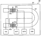
- the current sensor 100 includes a U-shaped conductor 102 in plan view provided on a substrate 101, GMR elements 103a and 103b provided at one end of the conductor 102, and a GMR provided at the other end. Elements 103c and 103d are provided.
- the magnetization directions of the ferromagnetic fixed layers are aligned in the same direction (see the arrow in FIG. 1), and form a magnetic field detection bridge circuit.
- an induced magnetic field applied from opposite directions to each other at one end and the other end of the U-shaped conductor 102 is detected via four GMR elements 103a to 103d.
- the output signals output from the pair of GMR elements 103 a and 103 b at one end of the conductor 102 In order to measure the current to be measured via the magnetic field detection bridge circuit, the output signals output from the pair of GMR elements 103 a and 103 b at one end of the conductor 102, The output signals output from the other pair of GMR elements 103c and 103d at the other end need to have different signal strengths. For this reason, in the current pull-in type current sensor 100, the conductor 102 is U-shaped, and a current to be measured is passed from one end of the conductor 102 to the other end. The direction in which the current to be measured flows is opposite to the direction in which the current to be measured flows at the other end.
- the direction in which the induced magnetic field is applied to the pair of GMR elements 103a and 103b and the direction in which the induced magnetic field is applied to the other pair of GMR elements 103c and 103d are opposite to each other, and thus the pair of GMR elements 103a and 103b.
- Output signals output from the other pair of output signals output from the other pair of GMR elements 103c and 103d have different signal strengths, and the current to be measured can be measured by the magnetic field detection bridge circuit.
- the output signals output from the pair of GMR elements 103a and 103b and the output signals output from the other pair of GMR elements 103c and 103d are different from each other.
- the current to be measured flows through the conductor 102 curved in a U-shape, interference is generated in the induced magnetic field, the measurement accuracy is lowered, and the resistance of the conductor 102 is increased, resulting in a loss of the current to be measured. Since heat generation occurs, there is a problem that the measurement range of the current to be measured is limited.
- the present inventors paid attention to the magnetic field strength of the induced magnetic field from the current to be measured applied to the magnetoresistive effect element and the application direction of the induced magnetic field.
- a conductor extending in one direction is used if an output signal with different signal strength can be obtained from a pair of magnetoresistive elements and another pair of magnetoresistive elements. Even in such a case, the current to be measured can be measured by the magnetic field detection bridge circuit.
- the present inventors paid attention to a self-pinned magnetoresistive effect element that can fix the magnetization direction of the ferromagnetic pinned layer without using an antiferromagnetic layer.
- the self-pinned structure has a laminated structure including a ferromagnetic pinned layer 32, a nonmagnetic intermediate layer 36, and a free magnetic layer 37 as shown in FIG. A structure having no antiferromagnetic layer under the layer 32 is referred to.
- the ferromagnetic pinned layer 32 includes a first ferromagnetic film 33, an antiparallel coupling film 34, and a second ferromagnetic film 35, and the second ferromagnetic film 35 faces the nonmagnetic intermediate layer 36. is doing.
- the magnetization direction X of the ferromagnetic pinned layer 32 of the plurality of magnetoresistive effect elements provided on the substrate can be fixed in an arbitrary direction. It becomes.
- the present inventors also have a pair of magnetoresistive effect elements and another pair of magnetoresistive elements.
- the pair of magnetoresistance effect elements and the other pair of magnetoresistance effect elements are different from each other. It has been found that an output signal of signal strength can be obtained. This makes it possible to measure the current to be measured by the magnetic field detection bridge circuit using the output signals from the pair of magnetoresistive elements and the output signals from the other pair of magnetoresistive elements.
- Such a configuration can be realized by using at least two pairs of self-pinning type magnetoresistive effect elements in a current drawing type current sensor that draws a current to be measured into a conductor on a substrate.
- the present inventors can reduce the size of the substrate and reduce the size of the current sensor by using a conductor extending in one direction in the current-drawing type current sensor.
- the inventors have found that interference can be reduced and measurement accuracy can be improved, and that induced electromotive force against an external magnetic field can be suppressed, and the present invention has been completed.
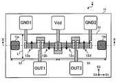
- FIG. 2 is a schematic plan view of the current sensor 1 according to the first embodiment of the present invention.
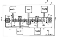
- the current sensor 1 according to the present embodiment includes a substrate 11 and four magnetoresistive elements 12 a that are arranged on the substrate 11 and output an output signal by an induced magnetic field from a current to be measured.
- the conductor 13 is provided so as to extend in one direction along the magnetoresistive effect elements 12a to 12d arranged in parallel on the substrate 11, and electrode pads 13a for drawing a current to be measured from the outside to both ends. 13b is provided.
- a current to be measured that is drawn from the outside through the electrode pads 13a and 13b and flows through the conductor 13 in one direction includes four magnetoresistive effect elements 12a to 12d. It measures with the magnetic field detection bridge circuit which becomes.
- the conductor 13 has, in the extending direction D1, a first section S1 and a second section S2 having different cross-sectional areas in the vertical section along the height direction D3 orthogonal to the extending direction D1.
- the conductor 13 electrode pad 13a side is defined as a first section S1 having a relatively large cross-sectional area
- electrode pad 13b side is defined as a second section S2 having a relatively small cross-sectional area.
- the magnetoresistance effect elements 12a to 12d are arranged so as to overlap the conductor 13 along the extending direction D1 of the conductor 13.
- the magnetoresistive effect elements 12a to 12d are disposed in the same plane (see FIG. 5), and the pair of magnetoresistive effect elements 12a and 12b are arranged along the first section S1 of the conductor 13.
- the other pair of magnetoresistive elements 12c and 12d are disposed along the second section S2 of the conductor 13.
- the magnetoresistive effect elements 12a to 12d output signals from the pair of magnetoresistive effect elements 12a and 12b and the other pair of magnetoresistive effect elements 12c and 12d by the induced magnetic field from the current to be measured. If the output signals are different in signal strength from each other, it is not always necessary to arrange them in the same plane.
- the sensitivity axes (Pin direction) of the pair of magnetoresistive effects 12a and 12b and the sensitivity axes (Pin direction) of the other pair of magnetoresistive effect elements 12c and 12d are antiparallel to each other ( 180 ° different directions).
- the pair of magnetoresistive elements 12a and 12b are arranged so that the sensitivity axes (Pin directions) of the magnetoresistive elements 12a and 12b are antiparallel to each other (direction different by 180 °).
- the magnetoresistive effect elements 12c and 12d are arranged so that the sensitivity axes (Pin directions) of the magnetoresistive effect elements 12c and 12d are antiparallel to each other (a direction different by 180 °).
- arrows attached to the magnetoresistive effect elements 12a to 12d indicate the magnetization directions of the second ferromagnetic films 35 (not shown in FIG. 1, refer to FIG. 6) of the magnetoresistive effect elements 12a to 12d.
- a hard bias layer 14 (FIG. 1) for applying a bias magnetic field to the free magnetic layer 37 (not shown in FIG. 1, see FIG. 6) of the magnetoresistive effect elements 12a to 12d. (Not shown, see FIG. 5). Note that the hard bias layer 14 is not necessarily provided.
- the magnetoresistive elements 12a to 12d are GMR elements having a shape (a meander shape) formed by folding a plurality of strip-like long patterns (stripes) arranged so that their longitudinal directions are parallel to each other. preferable.
- a power supply potential (Vdd) is applied to one terminal of the magnetoresistive effect element 12b and one terminal of the magnetoresistive effect element 12c, respectively, and one terminal of the magnetoresistive effect element 12a and the magnetoresistive effect element 12d.
- One terminal is supplied with a ground potential (GND1, GND2).
- GND1, GND2 ground potential
- the other terminal of the magnetoresistive effect element 12a and the other terminal of the magnetoresistive effect element 12b are connected to form a first output (Out1), and the other terminal of the magnetoresistive effect element 12c, and The other terminals of the magnetoresistive effect element 12c are connected to form a second output (Out2).
- the magnetoresistive effect elements 12a to 12d have a characteristic that the resistance value changes when an induced magnetic field from the current to be measured is applied, the first output (in accordance with the induced magnetic field from the current to be measured ( Out1) and the second output (Out2) change.
- the potential difference between the first output (Out1) and the second output (Out2) is proportional to the induced magnetic field, and the potential difference (voltage) becomes the output of the current sensor 1.
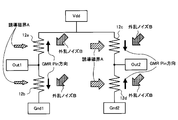
- FIG. 3 is a schematic diagram showing a magnetic detection bridge circuit in the current sensor according to the present embodiment.
- the magnetization directions (second second) of the ferromagnetic pinned layers 32 of the two magnetoresistive elements 12a and 12b that output the midpoint potential (Out1) are output.
- the magnetization direction (Pin2) of the ferromagnetic film is 180 ° different from each other (anti-parallel), and the magnetization direction (the first direction) of the ferromagnetic pinned layer 32 of the two magnetoresistive effect elements 12c and 12d that output the midpoint potential (Out2).
- the magnetization directions of the two ferromagnetic films (Pin2) are 180 ° different from each other (antiparallel).
- the resistance change rates of the four magnetoresistive elements 12a to 12d are the same.
- the magnetoresistive effect elements 12a to 12d preferably exhibit the same rate of change in resistance at the same magnetic field strength when the angle of the applied magnetic field to the ferromagnetic pinned layer 32 is the same.
- 12d a pair of magnetoresistive elements 12a and 12b constitutes a first half bridge circuit
- another pair of magnetoresistive elements 12c and 12d constitutes a second half bridge circuit.
- the conductor 13 has a cross-sectional area in the first section S1 in the vicinity of the magnetoresistive effect elements 12a and 12b in the second section in the vicinity of the magnetoresistive effect elements 12c and 12d. Since it is larger than the cross-sectional area of the conductor 13 in S2, an induced magnetic field A having a relatively small magnetic field strength is applied to the magnetoresistive elements 12a and 12b.
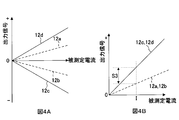
- FIG. 4 is a conceptual diagram showing the correlation between the magnitude of the current to be measured and the output signals from the magnetoresistive elements 12a to 12d.
- the horizontal axis represents the magnitude of the induced magnetic field
- the vertical axis represents the magnitude of the output signal.
- the output signals output from the pair of magnetoresistive effect elements 12a and 12b arranged along the first section S1 of the conductor 13 are in opposite phases and have the same strength (see FIG. 4A). (See dashed line 4A).
- the output signals output from the other pair of magnetoresistive elements 12c and 12d disposed along the second section S2 of the conductor 13 are in reverse phase with each other, have the same strength, and have a pair of magnetic fields. It becomes relatively large with respect to the output signals output from the resistance effect elements 12a and 12b (see the solid line in FIG. 4A). For this reason, as shown in FIG.
- the magnetization directions of the ferromagnetic pinned layers 32 of the magnetoresistive effect elements 12a and 12d are made the same, and the ferromagnetic pinned layers of the magnetoresistive effect elements 12a and 12d are aligned.
- the magnetization direction of 32 the magnetization direction of the ferromagnetic fixed layer 32 of the magnetoresistive effect elements 12b and 12c is aligned in an antiparallel direction (a direction different by 180 °).
- the output signals output from the pair of magnetoresistive elements 12a and 12b by the induced magnetic field A and the output signals output from the other pair of magnetoresistive elements 12c and 12d are reversed in phase
- the output signals output from the pair of magnetoresistive elements 12a and 12b due to the disturbance noise B are equal to the output signals output from the other pair of magnetoresistive elements 12c and 12d. Therefore, by obtaining a differential output between the output signals from the pair of magnetoresistive elements 12a and 12b and the output signals from the other pair of magnetoresistive elements 12c and 12d, Since addition and disturbance noise can be canceled, measurement accuracy and detection sensitivity can be improved. Therefore, a current sensor with high detection sensitivity and measurement accuracy can be realized.
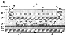
- FIG. 5 is a cross-sectional view taken along line VV of the current sensor 1 shown in FIG.
- a magnetic field detection bridge circuit magnetoresistance effect elements 12a to 12d
- a conductor 13 are stacked on the same substrate 11.
- a silicon oxide film 21 that is an insulating layer is formed on a substrate 11.
- An aluminum oxide film 22 is formed on the silicon oxide film 21.
- the aluminum oxide film 22 can be formed by a method such as sputtering. Further, a silicon substrate or the like is used as the substrate 11.
- magnetoresistive effect elements 12a to 12d are arranged to form a magnetic field detection bridge circuit.
- the magnetoresistive elements 12a to 12d TMR elements (tunnel type magnetoresistive elements), GMR elements (giant magnetoresistive elements), and the like can be used.
- Hard bias layers 14 for applying a bias magnetic field to the free magnetic layer 37 of the magnetoresistive effect elements 12a to 12d are provided at both ends of the magnetoresistive effect elements 12a to 12d.
- a conductor 13 (current line to be measured) is laminated via an insulating layer 23.
- the conductor 13 can be formed by photolithography and plating after forming a base material by sputtering or the like.
- Electrodes 13 a and 13 b are formed at both ends of the conductor 13.
- the electrode pads 13a and 13b can be formed by photolithography and plating after forming an electrode material.
- a polyimide layer formed by applying and curing a polyimide material can be used.
- a high magnetic permeability material such as an amorphous magnetic material, a permalloy magnetic material, or an iron microcrystalline material can be used.
- a silicon oxide film 26 is laminated on the magnetic shield 25.
- the silicon oxide film 26 can be formed by a method such as sputtering.
- a contact hole 27 is formed in a predetermined region of the insulating layer 24 and the silicon oxide film 26 (region where the electrode pads 13a and 13b are formed), and the electrode pads 13a and 13b are formed in the contact hole 27.
- photolithography, etching, or the like is used for forming the contact hole 27.
- the magnetic detection bridge circuit is configured by the four magnetoresistive effect elements 12a to 12d having the same film configuration, the zero magnetic field resistance value (R 0 ) between the elements and the resistance temperature coefficient ( TCR 0 ) can be eliminated. For this reason, variation in the midpoint potential can be reduced regardless of the environmental temperature, and current measurement can be performed with high accuracy.
- the current sensor 1 having the above configuration can be reduced in size because the conductor 13, the magnetic shield 25, and the magnetic field detection bridge circuit (the magnetoresistive effect elements 12a to 12d) are stacked on the same substrate. . Furthermore, since the current sensor 1 has a configuration without a magnetic core, it can be reduced in size and cost.
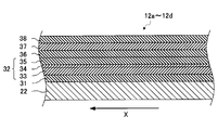
- FIG. 6 is a schematic cross-sectional view showing a laminated structure of magnetoresistive elements 12a to 12d of the current sensor 1 according to the present embodiment.
- the magnetoresistive effect elements 12a to 12d are stacked on the aluminum oxide film 22.
- the magnetoresistive effect elements 12a to 12d include a seed layer 31, a ferromagnetic pinned layer 32 (a first ferromagnetic film 33, an antiparallel coupling film 34, and a second ferromagnetic film 35), a nonmagnetic intermediate layer 36, a free layer
- the magnetic layer 37 and the protective layer 38 are laminated in this order.
- the first ferromagnetic film 33 and the second ferromagnetic film 35 are antiferromagnetically coupled via the antiparallel coupling film 34, so-called self-pinning type.
- a ferromagnetic pinned layer 32 (SFP: Synthetic Ferri Pinned layer) is formed.
- SFP Synthetic Ferri Pinned layer
- Annealing in a magnetic field for fixing the magnetization direction of a certain ferromagnetic pinned layer 32 becomes unnecessary, and the induced magnetic anisotropy in the stripe longitudinal direction D1 imparted during the formation of the free magnetic layer 37 can be maintained. Thereby, it becomes possible to reduce hysteresis with respect to the detection target direction.
- the thickness of the antiparallel coupling film 34 is set to 0.3 nm to 0.45 nm, or 0.75 nm to 0.95 nm, so that the first ferromagnetic film 33 and the second ferromagnetic film 33 Strong antiferromagnetic coupling with the ferromagnetic film 35 can be brought about.
- the magnetization amount (Ms ⁇ t) of the first ferromagnetic film 33 and the magnetization amount (Ms ⁇ t) of the second ferromagnetic film 35 are substantially the same. That is, the difference in magnetization between the first ferromagnetic film 33 and the second ferromagnetic film 35 is substantially zero. For this reason, the effective anisotropic magnetic field of the ferromagnetic fixed layer 32 is large. Therefore, sufficient magnetization stability of the ferromagnetic pinned layer 32 can be ensured without using an antiferromagnetic material.
- the magnetoresistive effect elements 12a to 12d used in the current sensor 1 have a film configuration that does not have an antiferromagnetic layer.
- Formula (1) eff Hk 2 (K ⁇ t 1 + K ⁇ t 2 ) / (Ms ⁇ t 1 ⁇ Ms ⁇ t 2 )
- the Curie temperature (Tc) of the first ferromagnetic film 33 and the Curie temperature (Tc) of the second ferromagnetic film 35 are the same. Thereby, even in a high temperature environment, the difference in magnetization (Ms ⁇ t) between the first ferromagnetic film 33 and the second ferromagnetic film 35 becomes zero, and high magnetization stability can be maintained.
- the first ferromagnetic film 33 is preferably made of a CoFe alloy containing 40 atomic% to 80 atomic% of Fe. This is because a CoFe alloy having this composition range has a large coercive force and can stably maintain magnetization with respect to an external magnetic field.
- the second ferromagnetic film 35 is preferably composed of a CoFe alloy containing 0 atomic% to 40 atomic% of Fe. This is because the CoFe alloy having this composition range has a small coercive force and is easily magnetized in an antiparallel direction (a direction different by 180 °) with respect to the direction in which the first ferromagnetic film 33 is preferentially magnetized. is there.
- a magnetic field is applied to the first ferromagnetic film 33 and the second ferromagnetic film 35 in the stripe width direction of the meander shape during the film formation, and the first ferromagnetic film 33 and the second strong film after the film formation are applied. It is preferable that induced magnetic anisotropy is imparted to the magnetic film 35. As a result, the first ferromagnetic film 33 and the second ferromagnetic film 35 are magnetized antiparallel to the stripe width direction.
- the magnetization directions (directions in which the magnetization is fixed) of the first ferromagnetic film 33 and the second ferromagnetic film 35 are determined by the magnetic field application direction when the first ferromagnetic film 33 is formed. It is possible to form a plurality of magnetoresistive elements having ferromagnetic pinned layers having different magnetization directions on the same substrate by changing the direction of magnetic field application during the formation of the ferromagnetic film 33.
- the seed layer 31 is made of NiFeCr or Cr.
- the protective layer 38 is made of T or the like.
- the aluminum oxide film 22 and the seed layer 31 are made of a nonmagnetic material such as at least one element of Ta, Hf, Nb, Zr, Ti, Mo, and W, for example.
- An underlayer may be provided.
- the antiparallel coupling film 34 of the ferromagnetic pinned layer 32 is made of Ru or the like.
- the free magnetic layer (free layer) 37 is made of a magnetic material such as a CoFe alloy, a NiFe alloy, or a CoFeNi alloy.
- the nonmagnetic intermediate layer 36 is made of Cu or the like. Further, it is preferable that a magnetic field is applied to the free magnetic layer 37 in the stripe longitudinal direction D1 during film formation, and induced magnetic anisotropy is imparted to the free magnetic layer 37 after film formation.
- the resistance is linearly changed with respect to the external magnetic field (magnetic field from the current to be measured) in the stripe width direction orthogonal to the stripe longitudinal direction D1, and the hysteresis can be reduced. it can.
- a spin valve configuration is adopted by the ferromagnetic pinned layer 30, the nonmagnetic intermediate layer 36 and the free magnetic layer 37.
- the film configuration of the magnetoresistive effect elements 12a to 12d used in the current sensor 1 for example, NiFeCr (seed layer 31: 5 nm) / Fe 70 Co 30 (first ferromagnetic film 33: 1.65 nm) / Ru (anti-parallel coupling film 34: 0.4 nm) / Co 90 Fe 10 (second ferromagnetic film 35: 2 nm) / Cu (nonmagnetic intermediate layer 36: 2.2 nm) / Co 90 Fe 10 (free magnetic layer 37: 1 nm) / Ni 81 Fe 19 (free magnetic layer 37: 7 nm) / Ta (protective layer 38: 5 nm).
- the first ferromagnetic film 33 and the second ferromagnetic film 35 are anti-bonded on the aluminum oxide film 22 via the anti-parallel coupling film 34.
- a magnetoresistive effect element 12a to 12 having a self-pinned ferromagnetic fixed layer 32, a nonmagnetic intermediate layer 36, and a free magnetic layer 37 that are ferromagnetically coupled and whose magnetization direction is fixed in a specific direction.
- first forming step the first laminated film in a region other than the region where the first laminated film is left is removed from the aluminum oxide film 22 (removing step), and the first laminated film is removed.
- Self-pinning type ferromagnetic pinning in which the first ferromagnetic film 33 and the second ferromagnetic film 35 are antiferromagnetically coupled to the removed aluminum oxide film 22 via the antiparallel coupling film 34.
- the magnetoresistive effect elements 12 a and 12 b having different magnetization directions of the ferromagnetic pinned layer 32 can be provided close to each other on the same substrate 11. Further, by repeatedly performing the removing step and the second forming step, it is possible to provide a plurality of magnetoresistive elements 12a to 12d having different magnetization directions of the ferromagnetic pinned layer 32 on the same substrate 11.
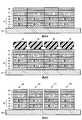
- FIGS. 7A to 7C and FIGS. 8A to 8C are explanatory diagrams of a method of manufacturing the magnetoresistive effect elements 12a to 12d in the current sensor 1 according to the present embodiment.
- the magnetoresistive effect elements 12b and 12c are formed after the magnetoresistive effect elements 12a and 12d are formed.
- a seed layer 31 on the aluminum oxide film 22, a seed layer 31, a first ferromagnetic film 33, an antiparallel coupling film 34, a second ferromagnetic film 35, a nonmagnetic intermediate layer 36, a free magnetic layer.
- a layer 37 and a protective layer 38 are sequentially formed.
- a magnetic field is applied in the meander-shaped stripe width direction. 7A to 7C, with respect to the first ferromagnetic film 33 (Pin1), the applied magnetic field direction is the direction from the back side to the near side of the paper, and the second ferromagnetic film 35 (Pin2) is applied.
- the direction of the magnetic field is the direction from the front side to the back side of the page.
- the same direction as the first ferromagnetic film 33 or no magnetic field may be used.
- a resist layer 40 is formed on the protective layer 38, and the resist layer 40 is left on the regions of the magnetoresistive effect elements 12a and 12d by photolithography and etching.
- the exposed laminated film is removed by ion milling or the like to expose the aluminum oxide film 22 in the region where the magnetoresistive effect elements 12b and 12c are provided.
- the seed layer 31 After removing the resist layer 40, the seed layer 31, the first ferromagnetic film 33, the antiparallel coupling film 34, and the second ferromagnetic material are formed on the exposed aluminum oxide film 22.
- a magnetic field is applied in the meander-shaped stripe width direction.
- the direction of the applied magnetic field is the direction from the back side to the front side of the page, and the magnetoresistive effect 12b
- the direction of the applied magnetic field is the direction from the front side of the page toward the back side of the page.
- the direction of the applied magnetic field is the direction from the front side to the back side of the paper surface, and the second ferromagnetic film 35 that becomes the magnetoresistive effects 12b and 12c.
- the applied magnetic field direction is the direction from the back side to the front side of the drawing.
- a magnetic field is applied in the longitudinal direction of the meander stripe.
- a resist layer 40 is formed on the protective layer 38, and the resist layer 40 is left on the formation regions of the magnetoresistive effect elements 12a, 12b, 12c, and 12d by photolithography and etching.
- the exposed laminated film is removed by ion milling or the like, and magnetoresistive effect elements 12a, 12b, 12c, and 12d are formed in an arrangement as shown in FIG.
- the magnetization direction of the ferromagnetic fixed layer 32 without providing an antiferromagnetic layer. can be fixed in any direction, so that the magnetization direction of the ferromagnetic pinned layer 32 of each of the magnetoresistive effect elements 12a to 12d can be set to an arbitrary direction even when four magnetoresistive effect elements are arranged in parallel on the substrate. Can be fixed.
- a current-drawing type current sensor using a conductor extending in one direction can be realized, so that the current to be measured flows through the conductor 13 as compared with the case where a conductor having a curved shape is used.
- the resistance due to the conductor 13 can be reduced, and the loss of the current to be measured and the heat generation due to the flow of the current to be measured can be suppressed. Furthermore, since the direction of the induced magnetic field from the current to be measured can be aligned, it is possible to suppress the interference of the induced magnetic field and the generation of induced electromotive force against the disturbance magnetic field, and a current sensor with a wide measurement range and high measurement accuracy can be obtained. realizable.
- the pair of magnetoresistive elements 12a and 12b are disposed along the first section S1 having a relatively large cross-sectional area of the conductor 13, and the other pair of magnetoresistive elements. Since 12c and 12d are disposed along the second section S2 having a relatively small cross-sectional area, an induced magnetic field applied to the pair of magnetoresistive elements 12a and 12b and another pair of magnetoresistances The effect elements 12c and 12d and the induced magnetic field applied have different magnetic field strengths. Accordingly, the output signals output from the pair of magnetoresistive effect elements 12a and 12b and the output signals output from the other pair of magnetoresistive effect elements 12c and 12d have different signal strengths.
- the measured current can be measured by the magnetic field detection bridge circuit without using.
- the magnetization direction of the ferromagnetic pinned layer 32 of the pair of magnetoresistive effect elements 12a and 12b and the magnetization direction of the ferromagnetic pinned layer 32 of the other pair of magnetoresistive effect elements 12c and 12d are fixed in the same direction. Therefore, the output signals output from the pair of magnetoresistance effect elements 12a and 12b and the output signals output from the other pair of magnetoresistance effect elements 12c and 12d are in phase due to disturbance noise. Furthermore, due to the current to be measured, the induced magnetic field applied to the pair of magnetoresistive effect elements 12a and 12b and the induced magnetic field applied to the other pair of magnetoresistive effect elements 12c and 12d have different magnetic field strengths.
- the differential output is appear.
- an output signal derived from an induced magnetic field from the current to be measured is obtained by a differential output between the output signals of the pair of magnetoresistive effect elements 12a and 12b and the output signals of the other pair of magnetoresistive effect elements 12c and 12d.
- disturbance noise components are canceled out, so that a current sensor with high detection sensitivity and high measurement accuracy can be realized.
- the magnetic field detection bridge circuit can be configured without using a fixed resistance element, so that offset can be reduced and a conductor extending in one direction can be used. Since the current to be measured can be measured, the area of the substrate can be reduced, and the current sensor can be downsized and the manufacturing cost can be reduced. In addition, since it is possible to configure the magnetoresistive element without using an antiferromagnetic material, it is possible to ensure the stability of the operation of the current sensor 1 even in a high temperature environment and not to use an antiferromagnetic material. Therefore, it is possible to reduce the manufacturing cost because the material cost and the annealing process in the magnetic field are not required.
- the magnetic detection bridge circuit is composed of four magnetoresistive effect elements having the same film configuration, the zero magnetic field resistance value (R 0 ) and the resistance temperature coefficient between the elements.
- the deviation of (TCR 0 ) can be eliminated. For this reason, the variation in the midpoint potential can be reduced regardless of the environmental temperature, and the measurement accuracy of the current to be measured can be improved.
- the pair of magnetoresistive elements 12a and 12b are disposed with the region on the electrode pad 13a side of the conductor 13 as the first section S1, and the region on the electrode pad 13b side of the conductor 13 is defined.
- the configuration in which the other pair of magnetoresistive effect elements 12c and 12d is provided as the second section S2 has been described.
- the arrangement of the magnetoresistive effect elements 12a to 12d is a pair of the magnetoresistive effect elements 12a and 12b and the other pair. As long as the arrangement is such that output signals having different signal strengths are output from the magnetoresistive effect elements 12c and 12d, the magnetoresistive effect elements 12c and 12d can be appropriately changed.
- both ends of the conductor 13 in the extending direction D1 are respectively set as the first section S1, and the pair of magnetoresistive effect elements 12a and 12b are respectively disposed, and the section between the first sections S1 is set as the second section S2.
- Another pair of magnetoresistive elements 12c and 12d may be provided.
- the first section S1 and the second section S2 are provided alternately from the electrode pad 13a side to the electrode pad 13b side of the conductor 13, thereby providing a pair of magnetoresistive elements. You may arrange
- the width dimension L1 of 1st area S1 and the width dimension L2 of 2nd area S2 are made into different magnitude
- the configuration of the conductor 13 having S2 has been described, a configuration in which the cross-sectional areas of the first section S1 and the second section S2 are made different from each other is a pair of magnetoresistance effect elements 12a and 12b and another pair of magnetoresistance effects. If output signals having different signal intensities are output from the elements 12c and 12d, they can be appropriately changed.
- the width dimensions L1 and L2 of the conductor 13 are the same, and the dimensions (thicknesses) in the height direction D3 perpendicular to the extending direction D1 and the width direction D2 of the conductor 13 are different from each other.
- the conductor 13 having the first section S1 and the second section S2 may be used.
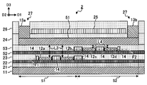
- FIG. 9 is a schematic plan view of the current sensor 2 according to the present embodiment
- FIG. 10 is a schematic cross-sectional view taken along the line XX in FIG.
- the conductor 51 is provided so as to extend in one direction, and has a uniform width dimension L1.
- the magnetoresistance effect elements 12a to 12d are arranged in parallel along the extending direction D1 of the conductor 51.
- the pair of magnetoresistive elements 12a and 12b are disposed in the first plane (see F1) in the first section S1, and the other pair of magnetoresistive elements 12c and 12d are second. In the section S2, it is disposed in the second plane (see F2).
- the distance L3 between the pair of magnetoresistance effect elements 12a and 12b and the conductor 13 in the height direction D3 of the conductor 13, and the other pair of magnetoresistance effect elements 12c and 12d Since the distance L4 between the conductor 13 and the conductor 13 is different from each other, the induced magnetic field applied to the pair of magnetoresistive elements 12a and 12b and the induced magnetic field applied to the other pair of magnetoresistive elements 12c and 12d And have different magnetic field strengths. As a result, the output signals output from the pair of magnetoresistive elements 12a and 12b and the output signals output from the other pair of magnetoresistive elements 12c and 12d have different signal intensities.
- the current to be measured can be measured by the circuit.
- a silicon oxide film 21 is provided on the substrate 11, and magnetoresistive effect elements 12a and 12b are disposed on the silicon oxide film 21 via an aluminum oxide film 22.
- Hard bias layers 14 for applying a bias magnetic field to the free magnetic layers 37 of the magnetoresistive effect elements 12a and 12b are provided at both ends of the magnetoresistive effect elements 12a and 12b.
- An insulating layer 23, an aluminum oxide film 52, an insulating layer 53, a conductor 51, and the like are stacked on the magnetoresistive effect elements 12a and 12b.
- a silicon oxide film 21, an aluminum oxide film 22, and an insulating layer 23 are stacked in this order on the substrate 11, and the magnetoresistive effect element 12 c is formed on the insulating layer 23 via an aluminum oxide film 52. , 12d are disposed.
- Hard bias layers 14 for applying a bias magnetic field to the free magnetic layers 37 of the magnetoresistive effect elements 12c and 12d are provided at both ends of the magnetoresistive effect elements 12c and 12d.
- An insulating layer 53, a conductor 51, and the like are stacked on the magnetoresistive effect elements 12a and 12b. Since the other laminated structure is the same as that of the current sensor 1 according to the first embodiment, the description thereof is omitted.
- the current sensor 2 has a different stacked structure in the region on the electrode pad 13a side of the conductor 51 and the region on the electrode pad 13b side, and the pair of magnetoresistive effect elements 12a and 12b and the conductor 13 are provided. Is larger than the distance L4 between the other pair of magnetoresistive elements 12c and 12b and the conductor 13.
- the magnetic field strength of the induced magnetic field applied to the pair of magnetoresistive effect elements 12a and 12b is relative to the magnetic field strength of the induced magnetic field applied to the other pair of magnetoresistive effect elements 12c and 12d.
- the output signals output from the pair of magnetoresistive elements 12a and 12b and the output signals output from the other pair of magnetoresistive elements 12c and 12d have different signal strengths. It becomes possible to measure the current to be measured.
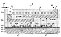
- FIG. 11 is a schematic cross-sectional view of the current sensor 3 according to the present embodiment.
- the conductor 61 includes first and second conductive paths 61a and 61b extending in the same direction, and the first conductive path 61a and the second conductive path 61b. And a third conductive path 61c to be connected.
- the first and second conductive paths 61a and 61b are provided so as to extend parallel to the surface of the substrate 11, and the relative positions in the height direction D3 orthogonal to the extending direction D1 of the conductor 61 are They are provided differently.
- the first conductive path 61a is the first section S1
- the second conductive path 61b is the second section S2.
- the conductor 61 is provided such that the distance between the surface of the substrate 11 and the first conductive path 61a is smaller than the distance between the surface of the substrate 11 and the second conductive path 61b. It is done.
- An electrode pad 13a is provided on one end side of the first conductive path 61a, and an electrode pad 13b is provided on the other end side of the second conductive path 61b.
- the other end of the first conductive path 61a and one end of the second conductive path 61b are connected by a third conductive path 61c.
- the magnetoresistive elements 12a to 12d are juxtaposed along the extending direction of the conductor 61, and are arranged in the same plane (see F3).
- a pair of magnetoresistive elements 12a and 12b are disposed along the first conductive path 61a, and the other pair of magnetoresistive elements 12c and 12d are disposed along the second conductive path 61b. .
- the distance L5 between the pair of magnetoresistive elements 12a and 12b and the first conductor 61a is other than It arrange
- the magnetoresistive effect elements 12a to 12d are output from the pair of magnetoresistive effect elements 12a and 12b and the other pair of magnetoresistive effect elements 12c and 12d by the induced magnetic field from the current to be measured.
- the configuration is not limited to the configuration in which the output signals are arranged in the same plane.
- the distance L5 between the pair of magnetoresistive elements 12a and 12b and the first conductive path 61a is equal to the other pair of magnetoresistive elements 12c
- the distance L6 is smaller than the distance L6 between 12d and the second conductive path 61b
- the magnetic field strength of the induced magnetic field applied to the pair of magnetoresistive elements 12a and 12b is different from that of the other pair of magnetoresistive elements 12c.
- 12d becomes relatively large with respect to the magnetic field strength of the induction magnetic field applied to 12d.
- the output signals output from the pair of magnetoresistive elements 12a and 12b and the output signals output from the other pair of magnetoresistive elements 12c and 12d have different signal strengths. It becomes possible to measure the current to be measured.
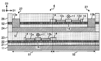
- FIG. 12 is a schematic cross-sectional view of the current sensor 4 according to the present embodiment.
- the pair of magnetoresistive elements 12a and 12b and the other pair of magnetoresistive elements 12c and 12d have an application direction of an induced magnetic field from the current I to be measured. It arrange
- the pair of magnetoresistive elements 12a and 12b are arranged on the lower surface side in the first section S1 on the electrode pad 13a side of the conductor 13 with respect to the extending direction of the conductor 13 in a sectional view.
- the other pair of magnetoresistive elements 12c and 12d are disposed on the upper surface side in the second section S2 on the electrode pad 13b side of the conductor 13 with respect to the extending direction of the conductor 13 in a sectional view.
- the induced magnetic field when the current I to be measured flows through the conductor 13 from the electrode pad 13a side to the electrode pad 13b side is from the front side of the sheet with respect to the pair of magnetoresistive effect elements 12a and 12b. It is applied toward the back side of the paper, and applied to the other pair of magnetoresistive elements 12c and 12d from the back side of the paper toward the front of the paper.
- the output signals output from the pair of magnetoresistive elements 12a and 12b and the output signals output from the other pair of magnetoresistive elements 12b are out of phase, so that the current to be measured can be measured. It becomes.
- a silicon oxide film 21 is provided on the substrate 11, and magnetoresistive effect elements 12a and 12b are disposed on the silicon oxide film 21 via an aluminum oxide film 22.
- Hard bias layers 14 for applying a bias magnetic field to the free magnetic layers 37 of the magnetoresistive effect elements 12a and 12b are provided at both ends of the magnetoresistive effect elements 12a and 12b.
- the insulating layer 24, the conductor 13, the insulating layer 24, the aluminum oxide film 52, and the silicon oxide film 26 are laminated in this order.
- a silicon oxide film 21, an aluminum oxide film 22, an insulating layer 23, a conductor 13, and an insulating layer 24 are stacked in this order on the substrate 11, and an aluminum oxide film is formed on the insulating layer 24.
- the magnetoresistive effect elements 12 c and 12 d are disposed via 52.
- Hard bias layers 14 for applying a bias magnetic field to the free magnetic layers 37 of the magnetoresistive effect elements 12c and 12d are provided at both ends of the magnetoresistive effect elements 12c and 12d.
- a silicon oxide film 26 is laminated on the magnetoresistive effect elements 12c and 12d.
- the other laminated structure is the same as that of the current sensors 1, 2, and 3 according to the first, second, and third embodiments, and thus the description thereof is omitted.
- the pair of magnetoresistive elements 12a and 12b and the other pair of magnetoresistive elements 12c and 12d apply an induced magnetic field from the current to be measured. It arrange
- the direction in which the induction magnetic field is applied to the pair of magnetoresistance effect elements 12a and 12b and the direction in which the induction magnetic field is applied to the other pair of magnetoresistance effect elements 12c and 12d are different from each other.
- the output signals output from the resistance effect elements 12a and 12b and the output signals output from the other pair of magnetoresistance effect elements 12c and 12d have different signal strengths. As a result, the current to be measured can be detected by the magnetic field detection bridge circuit.
- the present invention has the effect of realizing a current sensor that has excellent operational stability at high temperatures and high measurement accuracy, and in particular, various current sensors and current sensors that detect the magnitude of current for driving motors in electric vehicles. It is possible to apply to.
Landscapes
- Physics & Mathematics (AREA)
- General Physics & Mathematics (AREA)
- Chemical & Material Sciences (AREA)
- Engineering & Computer Science (AREA)
- Nanotechnology (AREA)
- Condensed Matter Physics & Semiconductors (AREA)
- Crystallography & Structural Chemistry (AREA)
- Measuring Magnetic Variables (AREA)
- Measuring Instrument Details And Bridges, And Automatic Balancing Devices (AREA)
- Hall/Mr Elements (AREA)
Abstract
高温での動作安定性に優れ、測定精度が高い電流センサを提供すること。本発明の電流センサ(1)は、一方向に延在する導電体(13)と、導電体(13)の延在方向に沿って並設され導電体(13)を通流する被測定電流からの誘導磁界により出力信号を出力する磁気抵抗効果素子(12a)~(12d)とを具備し、磁気抵抗効果素子(12a)~(12d)は、導電体(13)の第1区間(S1)に沿って配設される一対の磁気抵抗効果素子(12a)、(12b)と、導電体13の第2区間(S2)に沿って配設される他の一対の磁気抵抗効果素子(12c)、(12d)と、を含み、一対の磁気抵抗効果素子(12a)、(12b)と他の一対の磁気抵抗効果素子(12c)、(12d)とは、誘導磁界が互いに異なる強度で印加され、又は誘導磁界が互いに異なる方向から印加されるように配設されたことを特徴とする。
Description
本発明は、電流の大きさを測定する電流センサに関し、例えば、磁気抵抗効果素子(TMR素子、GMR素子)を備えた電流センサに関する。
従来、電気自動車やハイブリッドカーにおけるモータ駆動技術などの分野では、モータの駆動電流を非接触で測定することが可能な電流センサが求められている。このような電流センサとして、被測定電流からの誘導磁界により出力信号を出力する磁気抵抗効果素子が備えたものが提案されている(例えば、特許文献1参照)。
特許文献1記載の電流センサは、4つの磁気抵抗効果素子で構成されるホイートストンブリッジ回路を備える。このホイートストンブリッジ回路においては、互いに逆相の出力信号が得られるように構成された二対の磁気抵抗効果素子からの出力信号により被測定電流を測定する。
ところで、特許文献1記載の電流センサにおいては、被測定電流の測定にホイートストンブリッジ回路を用いることから、二対の磁気抵抗効果素子から互いに異なる信号強度の出力信号を得る必要がある。このため、特許文献1記載の電流センサにおいては、被測定電流からの誘導磁界の印加方向に対して、二対の磁気抵抗効果素子の強磁性固定層の磁化方向を異なる方向に固定することにより、二対の磁気抵抗効果素子から出力される出力信号を逆相とすることで、被測定電流の測定を可能としている。
しかしながら、特許文献1記載の電流センサにおいては、二対の磁気抵抗効果素子の強磁性固定層の磁化方向が互いに異なるため、二対の磁気抵抗効果素子に外乱ノイズが作用した外乱ノイズ成分の影響で測定精度が低下する問題がある。また、磁気抵抗効果素子の強磁性固定層の磁化方向の固定するため、強磁性固定層と反強磁性層との間の交換結合磁界を用いることから、動作可能温度が制限されると共に、製造工程において、磁場中の高温アニール処理が必要となるので、製造コストが増大する問題がある。
本発明は、かかる点に鑑みてなされたものであり、高温での動作安定性に優れ、測定精度が高い電流センサを提供することを目的とする。
本発明の電流センサは、一方向に延在する導電体と、前記導電体の延在方向に沿って並設され前記導電体を通流する被測定電流からの誘導磁界により出力信号を出力する少なくとも二対の磁気抵抗効果素子とを具備し、前記磁気抵抗効果素子は、磁化方向が固定された強磁性固定層、非磁性中間層、及び外部磁界に対して磁化方向が変動するフリー磁性層を含む積層構造を有し、前記強磁性固定層が、反平行結合膜を介して第1の強磁性膜と第2の強磁性膜とを反強磁性的に結合させてなるセルフピン止め型であり、前記少なくとも二対の磁気抵抗効果素子は、前記導電体の第1区間に沿って配設される一対の磁気抵抗効果素子と、前記導電体の第2区間に沿って配設される他の一対の磁気抵抗効果素子と、を含み、前記一対の磁気抵抗効果素子と前記他の一対の磁気抵抗効果素子とは、前記誘導磁界が互いに異なる強度で印加され、又は前記誘導磁界が互いに異なる方向から印加されるように配設されたことを特徴とする。
この構成によれば、被測定電流からの誘導磁界により一対の磁気抵抗効果素子から出力される出力信号と、他の一対の磁気抵抗効果素子から出力される出力信号とが互いに異なる信号強度となるので、一対の磁気抵抗効果素子の出力信号と、他の一対の磁気抵抗効果素子の出力信号と、の差動出力を得ることにより、出力信号の外乱ノイズ成分を低減でき、測定精度が高い電流センサを実現できる。また、一方向に延在する導電体に被測定電流を通流するので、電流センサの小型化が可能となると共に、被測定電流からの誘導磁界の干渉を低減できるので電流センサの測定精度が更に向上する。さらに、被測定電流が通流する際の導電体の抵抗を小さくできるので、電流センサの測定範囲を拡大することが可能となる。また、セルフピン止め型の磁気抵抗効果素子を用いることから、反強磁性層を用いずに固定磁性層の磁化方向を固定できるので、高温での動作安定性に優れる電流センサを実現できる。
本発明の電流センサにおいては、前記一対の磁気抵抗効果素子を含む第1のハーフブリッジ回路と、前記他の一対の磁気抵抗効果素子を含む第2のハーフブリッジ回路とを具備し、前記第1のハーフブリッジ回路の各磁気抵抗効果素子における前記強磁性固定層の磁化方向と、前記第2のハーフブリッジ回路の各磁気抵抗効果素子における前記強磁性固定層の磁化方向と、が互いに同一であることが好ましい。この構成により、第1のハーフブリッジ回路から出力される出力信号中の外乱ノイズ成分と、第2のハーフブリッジ回路から出力される出力信号中の外乱ノイズ成分とが等しくなる。このため、二対の磁気抵抗効果素子の差動出力を得ることにより、外乱ノイズ成分を相殺でき、測定精度を更に向上できる。
本発明の電流センサにおいては、前記一対の磁気抵抗効果素子の前記強磁性固定層の磁化方向が互いに反平行であり、前記他の一対の磁気抵抗効果素子の前記強磁性固定層の磁化方向が互いに反平行であることが好ましい。この構成により、一対の磁気抵抗効果素子から出力される出力信号と、他の一対の磁気抵抗効果素子から出力される出力信号とが逆相となる。このため、二対の磁気抵抗効果素子の差動出力を得ることにより、誘導磁界により出力された出力信号が加算されるので、電流センサの検出感度を向上できる。なお、反平行とは、互いに180°異なる方向であって、逆方向のことをいう。
本発明の電流センサにおいては、前記導電体は、前記第1区間の前記延在方向に対する垂直断面における断面積と、前記第2区間の前記延在方向に対する垂直断面における断面積と、が異なることが好ましい。この構成により、一対の磁気抵抗効果素子に印加される誘導磁界と他の一対の磁気抵抗効果素子に印加される誘導磁界とが異なる磁界強度となるので、誘導磁界により一対の磁気抵抗効果素子から出力される出力信号と、他の一対の磁気抵抗効果素子から出力される出力信号とが異なる信号強度となる。このため、一対の磁気抵抗効果素子からの出力信号と、他の一対の磁気抵抗効果素子の出力信号を用いることで、被測定電流の測定が可能となる。
本発明の電流センサにおいては、前記一対の磁気抵抗効果素子と前記導電体の前記第1区間との間の距離と、前記他の一対の磁気抵抗効果素子と前記導電体の前記第2区間との間の距離と、が異なることが好ましい。この構成により、一対の磁気抵抗効果素子に印加される誘導磁界と他の一対の磁気抵抗効果素子に印加される誘導磁界とが異なる磁界強度となるので、誘導磁界により一対の磁気抵抗効果素子から出力される出力信号と、他の一対の磁気抵抗効果素子から出力される出力信号とが異なる信号強度となる。このため、一対の磁気抵抗効果素子からの出力信号と、他の一対の磁気抵抗効果素子の出力信号を用いることで、被測定電流の測定が可能となる。
本発明の電流センサにおいては、前記一対の磁気抵抗効果素子と、前記他の一対の磁気抵抗効果素子とは、前記誘導磁界が、互いに逆方向から印加されるように配設されたことが好ましい。この構成により、導電体の一方の面側に配設される一対の磁気抵抗効果素子対する誘導磁界の印加方向と、導電体の他方の面側に配設される他の一対の磁気抵抗効果素子に対する誘導磁界の印加方向とが、互いに逆方向となる。このため、一対の磁気抵抗効果素子から出力される出力信号と、他の一対の磁気抵抗効果素子から出力される出力信号とが異なる信号強度及び逆相となるので、二対の磁気抵抗効果素子の差動出力をとることで、外乱ノイズ成分が除去され、誘導磁界からの出力信号が加算されるので、測定精度が高い電流センサを実現できる。
本発明によれば、高温での動作安定性に優れ、測定精度が高い電流センサを提供することができる。
近年、電流センサの更なる小型化及び測定精度の向上が求められている。電流センサの小型化のため、基板上に設けた導電体パターンに被測定電流を引き込んで被測定電流を測定する電流引き込み型の電流センサが検討されている。
図1に電流引き込み型電流センサの一例を示す。かかる電流センサ100は、基板101上に設けられた平面視U字形状の導電体102と、この導電体102の一端部に設けられたGMR素子103a、103b、及び他端部に設けられたGMR素子103c、103dとを備える。4つのGMR素子103a~103dは、強磁性固定層の磁化方向が同一方向(図1の矢印参照)に揃えられており、磁界検出ブリッジ回路を構成している。この電流引き込み型電流センサ100においては、U字形状の導電体102の一端部及び他端部において、互いに逆方向から印加される誘導磁界を4つのGMR素子103a~103dを介して検出する。
電流引き込み型電流センサ100においては、磁界検出ブリッジ回路を介して被測定電流を測定するため、導電体102の一端部における一対のGMR素子103a、103bから出力される出力信号と、導電体102の他端部における他の一対のGMR素子103c、103dから出力される出力信号と、を互いに異なる信号強度とする必要がある。このため、上記電流引き込み型電流センサ100においては、導電体102をU字形状とし、導電体102の一端部から他端部に被測定電流を通流することにより、導電体102の一端部における被測定電流の通流方向と、他端部における被測定電流の通流方向とが互いに逆方向となるようにする。これにより、一対のGMR素子103a、103bに対する誘導磁界の印加方向と、他の一対のGMR素子103c、103dに対する誘導磁界の印加方向と、が互いに逆方向となるので、一対のGMR素子103a、103bから出力される出力信号と、他の一対のGMR素子103c、103dから出力される出力信号と、が異なる信号強度となり、磁界検出ブリッジ回路による被測定電流の測定が可能となる。
また、上記電流引き込み型電流センサ100においては、4つのGMR素子103a~103dの強磁性固定層の磁化方向を同一方向に揃えているので、各GMR素子103a~103dの感度軸に対して同一方向から外乱ノイズが作用する。このため、一対のGMR素子103a、103bから出力される出力信号と、他の一対のGMR素子103c、103dから出力される出力信号との差分値をとることにより、外乱ノイズの影響をキャンセルすることが可能となる。
一方で、上記電流引き込み型の電流センサ100においては、一対のGMR素子103a、103bから出力される出力信号と、及び他の一対のGMR素子103c、103dから出力される出力信号と、を互いに異なる信号強度とするため、導電体102をU字形状に形成する必要があり、電流センサ100の小型化が制限される問題がある。また、U字形状に湾曲した導電体102に被測定電流を通流するため、誘導磁界に干渉が生じて測定精度が低下すると共に、導電体102の抵抗が増大して被測定電流の損失や発熱が生じるため、被測定電流の測定範囲が制限される問題があった。
本発明者らは、磁気抵抗効果素子に印加される被測定電流からの誘導磁界の磁界強度、及び誘導磁界の印加方向に着目した。電流引き込み型の電流センサにおいては、一対の磁気抵抗効果素子と、他の一対の磁気抵抗効果素子と、から異なる信号強度の出力信号を得ることができれば、一方向に延在する導電体を用いた場合においても、磁界検出ブリッジ回路による被測定電流の測定が可能となる。
また、本発明者らは、反強磁性層を用いずに強磁性固定層の磁化方向を固定できるセルフピン止め型の磁気抵抗効果素子に着目した。ここで、セルフピン止め型の構造とは、後述する図6に示すように、強磁性固定層32と、非磁性中間層36と、フリー磁性層37とを含む積層構造を有し、強磁性固定層32の下に反強磁性層を持たない構造をいう。強磁性固定層32は、第1の強磁性膜33と、反平行結合膜34と、第2の強磁性膜35とを含み、第2の強磁性膜35が、非磁性中間層36と面している。セルフピン止め型の磁気抵抗効果素子を電流引き込み型の電流センサに用いることにより、基板上に設ける複数の磁気抵抗効果素子の強磁性固定層32の磁化方向Xを任意の方向に固定することが可能となる。
本発明者らは、一方向に延在する導電体の延在方向に沿って少なくとも二対の磁気抵抗効果素子を並設した場合においても、一対の磁気抵抗効果素子及び他の一対の磁気抵抗効果素子を誘導磁界が互いに異なる強度で印加され、又は誘導磁界が互いに異なる方向から印加されるように配設することにより、一対の磁気抵抗効果素子及び他の一対の磁気抵抗効果素子から互いに異なる信号強度の出力信号が得られることを見出した。これにより、一対の磁気抵抗効果素子からの出力信号と、他の一対の磁気抵抗効果素子からの出力信号と、を用いた磁界検出ブリッジ回路による被測定電流の測定が可能となる。このような構成は、被測定電流を基板上の導電体に引き込む電流引き込み型の電流センサにおいて、少なくとも二対のセルフピン止め型の磁気抵抗効果素子を用いることで実現することができる。
さらに、本発明者らは、電流引き込み型の電流センサにおいて、一方向に延在する導電体を用いることにより、基板の大きさを低減でき電流センサの小型化が可能となること、誘導磁界の干渉を低減でき測定精度を向上できること、及び外部磁界に対する誘導起電力を抑制できること、などを見出し、本発明を完成するに至った。
以下、本発明の実施の形態について、添付図面を参照して詳細に説明する。
(第1の実施の形態)
図2は、本発明の第1の実施の形態に係る電流センサ1の平面模式図である。図2に示すように、本実施の形態に係る電流センサ1は、基板11と、この基板11上に並設され被測定電流からの誘導磁界により出力信号を出力する4つの磁気抵抗効果素子12a~12dと、絶縁層を介して磁気抵抗効果素子12a~12d上に積層される導電体13とを備える。導電体13は、基板11上に並設される磁気抵抗効果素子12a~12dに沿って一方向に延在するように設けられており、両端部に外部から被測定電流を引き込む電極パッド13a、13bが設けられている。本実施の形態に係る電流センサ1においては、電極パッド13a、13bを介して外部から引き込まれ導電体13を一方向に通流する被測定電流を、4つの磁気抵抗効果素子12a~12dを含んでなる磁界検出ブリッジ回路により測定する。
(第1の実施の形態)
図2は、本発明の第1の実施の形態に係る電流センサ1の平面模式図である。図2に示すように、本実施の形態に係る電流センサ1は、基板11と、この基板11上に並設され被測定電流からの誘導磁界により出力信号を出力する4つの磁気抵抗効果素子12a~12dと、絶縁層を介して磁気抵抗効果素子12a~12d上に積層される導電体13とを備える。導電体13は、基板11上に並設される磁気抵抗効果素子12a~12dに沿って一方向に延在するように設けられており、両端部に外部から被測定電流を引き込む電極パッド13a、13bが設けられている。本実施の形態に係る電流センサ1においては、電極パッド13a、13bを介して外部から引き込まれ導電体13を一方向に通流する被測定電流を、4つの磁気抵抗効果素子12a~12dを含んでなる磁界検出ブリッジ回路により測定する。
導電体13は、延在方向D1において、当該延在方向D1に対して直交する高さ方向D3に沿う垂直断面の断面積が互いに異なる第1区間S1と第2区間S2とを有する。本実施の形態においては、延在方向D1における電極パッド13a側の幅寸法L1が、電極パッド13b側の幅寸法L2に対して相対的に大きくなるように導電体13を設けることで、導電体13の電極パッド13a側を相対的に断面積が大きい第1区間S1とし、電極パッド13b側を相対的に断面積が小さい第2区間S2としている。
磁気抵抗効果素子12a~12dは、導電体13の延在方向D1に沿って導電体13と重畳するように配設される。本実施の形態においては、磁気抵抗効果素子12a~12dは、同一平面内に配設され(図5参照)、一対の磁気抵抗効果素子12a、12bが、導電体13の第1区間S1に沿って配設され、他の一対の磁気抵抗効果素子12c、12dが、導電体13の第2区間S2に沿って配設される。なお、磁気抵抗効果素子12a~12dは、被測定電流からの誘導磁界により、一対の磁気抵抗効果素子12a、12bから出力される出力信号と、他の一対の磁気抵抗効果素子12c、12dから出力される出力信号とが互いに異なる信号強度となる配置であれば、必ずしも同一平面内に配設する必要はない。
磁気抵抗効果素子12a~12dは、一対の磁気抵抗効果12a、12bの感度軸(Pin方向)と、他の一対の磁気抵抗効果素子12c、12dの感度軸(Pin方向)とが互いに反平行(180°異なる方向)となるように配設される。また、一対の磁気抵抗効果素子12a、12bは、当該磁気抵抗効果素子12a、12bの感度軸(Pin方向)が互いに反平行(180°異なる方向)となるように配設され、他の一対の磁気抵抗効果素子12c、12dは、当該磁気抵抗効果素子12c、12dの感度軸(Pin方向)が互いに反平行(180°異なる方向)となるように配設される。なお、図2において、磁気抵抗効果素子12a~12dに付された矢印は、磁気抵抗効果素子12a~12dの第2の強磁性膜35(図1において不図示、図6参照)の磁化方向を表している。各磁気抵抗効果素子12a~12dの両端部には、磁気抵抗効果素子12a~12dのフリー磁性層37(図1において不図示、図6参照)にバイアス磁界を印加するハードバイアス層14(図1において不図示、図5参照)が設けられている。なお、ハードバイアス層14は、必ずしも設ける必要はない。
磁気抵抗効果素子12a~12dとしては、その長手方向が互いに平行になるように配置された複数の帯状の長尺パターン(ストライプ)が折り返してなる形状(ミアンダ形状)を有するGMR素子であることが好ましい。
次に、図2に示す電流センサ1の磁界検出ブリッジ回路の接続について説明する。磁気抵抗効果素子12bの一方の端子、及び磁気抵抗効果素子12cの一方の端子にはそれぞれ電源電位(Vdd)が与えられており、磁気抵抗効果素子12aの一方の端子、及び磁気抵抗効果素子12dの一方の端子にはそれぞれ接地電位(GND1、GND2)が与えられている。また、磁気抵抗効果素子12aの他方の端子、及び磁気抵抗効果素子12bの他方の端子がそれぞれ接続されて第一の出力(Out1)となっており、磁気抵抗効果素子12cの他方の端子、及び磁気抵抗効果素子12cの他方の端子がそれぞれ接続されて第二の出力(Out2)となっている。
磁気抵抗効果素子12a~12dは、被測定電流からの誘導磁界が印加されることで抵抗値が変化するという特性を備えているため、被測定電流からの誘導磁界に応じて第一の出力(Out1)と第二の出力(Out2)が変化する。第一の出力(Out1)と第二の出力(Out2)との電位差は誘導磁界に比例し、当該電位差(電圧)が電流センサ1の出力となる。
図3は、本実施の形態に係る電流センサにおける磁気検出ブリッジ回路を示す模式図である。本実施の形態に係る電流センサ1においては、図3に示すように、中点電位(Out1)を出力する2つの磁気抵抗効果素子12a、12bの強磁性固定層32の磁化方向(第2の強磁性膜の磁化方向:Pin2)が互いに180°異なっており(反平行)、中点電位(Out2)を出力する2つの磁気抵抗効果素子12c、12dの強磁性固定層32の磁化方向(第2の強磁性膜の磁化方向:Pin2)が互いに180°異なっている(反平行)。また、4つの磁気抵抗効果素子12a~12dの抵抗変化率は同じである。磁気抵抗効果素子12a~12dは、強磁性固定層32に対する印加磁界の角度が同一である場合、同一磁界強度で同一の抵抗変化率を示すことが好ましい。
本実施の形態に係る電流センサ1においては、導電体13の幅寸法L1、L2が異なる区間S1、S2にそれぞれ一対の磁気抵抗効果素子12a、12bと、他の一対の磁気抵抗効果素子12c、12dとが設けられ、一対の磁気抵抗効果素子12a、12bにより第1のハーフブリッジ回路が構成され、他の一対の磁気抵抗効果素子12c、12dにより第2のハーフブリッジ回路が構成される。
図3に示すように、導電体13に被測定電流が通流されると、4つの磁気抵抗効果素子12a~12dには、それぞれ誘導磁界Aが印加される。ここで、本実施の形態に係る電流センサ1においては、導電体13は、磁気抵抗効果素子12a、12b近傍の第1区間S1における断面積が、磁気抵抗効果素子12c、12d近傍の第2区間S2における導電体13の断面積より大きいので、磁気抵抗効果素子12a、12bに対して相対的に磁界強度の小さい誘導磁界Aが印加される。このため、第1のハーフブリッジ回路を構成する一対の磁気抵抗効果素子12a、12bから出力される出力信号と、第2のハーフブリッジ回路を構成する他の一対の磁気抵抗効果素子12c、12dから出力される出力信号と、が異なる信号強度となるので、磁界検出ブリッジ回路により被測定電流の測定が可能となる。
ここで、図4を参照して、磁気抵抗効果素子12a~12dに誘導磁界が印加された際の出力信号について説明する。図4は、被測定電流の大きさと磁気抵抗効果素子12a~12dからの出力信号との相関を示す概念図である。同図においては、横軸に誘導磁界の大きさを示し、縦軸に出力信号の大きさを示している。
図4Aに示すように、導電体13の第1区間S1に沿って配設された一対の磁気抵抗効果素子12a、12bから出力される出力信号は、互いに逆相となり、同一強度となる(図4Aの破線参照)。一方、導電体13の第2区間S2に沿って配設された他の一対の磁気抵抗効果素子12c、12dから出力される出力信号は、互いに逆相となり、同一強度となると共に、一対の磁気抵抗効果素子12a、12bから出力される出力信号に対して相対的に大きくなる(図4Aの実線参照)。このため、図4Bに示すように、同じ大きさの被測定電流Iが通流する場合に、一対の磁気抵抗効果素子12a、12bを含む第1のハーフブリッジ回路からの出力信号と、他の一対の磁気抵抗効果素子12c、12dを含む第2のハーフブリッジ回路からの出力信号との間には、信号強度に差が生じる(S3参照)。これにより、磁界検出ブリッジ回路による被測定電流の測定が可能となる。
このように、本実施の形態に係る電流センサ1においては、磁気抵抗効果素子12a、12dの強磁性固定層32の磁化方向を同一に揃え、この磁気抵抗効果素子12a、12dの強磁性固定層32の磁化方向に対して、磁気抵抗効果素子12b、12cの強磁性固定層32の磁化方向を反平行方向(180°異なる方向)に揃える。この構成により、誘導磁界Aにより一対の磁気抵抗効果素子12a、12bから出力される出力信号と、他の一対の磁気抵抗効果素子12c、12dから出力される出力信号とが逆相になると共に、外乱ノイズBにより一対の磁気抵抗効果素子12a、12bから出力される出力信号と、他の一対の磁気抵抗効果素子12c、12dから出力される出力信号とが等しくなる。このため、一対の磁気抵抗効果素子12a、12bからの出力信号と、他の一対の磁気抵抗効果素子12c、12dからの出力信号との差動出力を得ることにより、誘導磁界Aによる出力信号の加算及び外乱ノイズの相殺が可能となるので、測定精度及び検出感度を向上できる。したがって、検出感度及び測定精度が高い電流センサを実現できる。
次に、電流センサ1の積層構造について詳細に説明する。図5は、図2に示す電流センサ1のV-V線における矢視断面図である。同図に示すように、本実施の形態に係る電流センサ1においては、磁界検出ブリッジ回路(磁気抵抗効果素子12a~12d)、及び導電体13が同一基板11上に積層されている。
図5に示す電流センサ1においては、基板11上に絶縁層であるシリコン酸化膜21が形成されている。シリコン酸化膜21上には、アルミニウム酸化膜22が形成されている。アルミニウム酸化膜22は、例えば、スパッタリングなどの方法により成膜することができる。また、基板11としては、シリコン基板などが用いられる。
アルミニウム酸化膜22上には、磁気抵抗効果素子12a~12dが配設され、磁界検出ブリッジ回路が形成される。磁気抵抗効果素子12a~12dとしては、TMR素子(トンネル型磁気抵抗効果素子)、GMR素子(巨大磁気抵抗効果素子)などを用いることができる。磁気抵抗効果素子12a~12dの両端部には、磁気抵抗効果素子12a~12dのフリー磁性層37にバイアス磁界を印加するハードバイアス層14が設けられる。
磁気抵抗効果素子12a~12d及びハードバイアス層14上には、絶縁層23を介して導電体13(被測定電流線)が積層される。導電体13は、下地材料をスパッタリング法などにより成膜した後に、フォトリソグラフィ及びめっきにより形成することができる。
導電体13上には、絶縁層24を介して磁気抵抗効果素子12a~12dへの外乱ノイズを吸収する磁気シールド25が設けられる。また、導電体13の両端部には、電極パッド13a、13bが形成される。電極パッド13a、13bは、電極材料を成膜した後に、フォトリソグラフィ及びめっきにより形成することができる。
絶縁層23、24としては、例えば、ポリイミド材料を塗布し、硬化することで形成したポリイミド層などを用いることができる。磁気シールド25を構成する材料としては、アモルファス磁性材料、パーマロイ系磁性材料、又は鉄系微結晶材料等の高透磁率材料を用いることができる。
磁気シールド25上には、シリコン酸化膜26が積層される。シリコン酸化膜26は、例えば、スパッタリングなどの方法により成膜することができる。
絶縁層24及びシリコン酸化膜26の所定の領域(電極パッド13a、13bの形成領域)にはコンタクトホール27が形成され、このコンタクトホール27に電極パッド13a、13bが形成されている。コンタクトホール27の形成には、フォトリソグラフィ及びエッチングなどが用いられる。
上記構成を有する電流センサ1は、磁気検出ブリッジ回路が膜構成の同じ4つの磁気抵抗効果素子12a~12dで構成されているので、素子間におけるゼロ磁場抵抗値(R0)や抵抗温度係数(TCR0)のズレを無くすことができる。このため、環境温度によらず中点電位のばらつきを小さくでき、高精度に電流測定を行うことができる。また、上記構成を有する電流センサ1は、導電体13、磁気シールド25及び磁界検出ブリッジ回路(磁気抵抗効果素子12a~12d)が同一基板上に積層されてなるので、小型化を図ることができる。さらに、この電流センサ1は、磁気コアを有しない構成であるので、小型化、低コスト化を図ることができる。
次に、図6を参照して本実施の形態に係る電流センサ1の積層構造について説明する。図6は、本実施の形態に係る電流センサ1の磁気抵抗効果素子12a~12dの積層構造を示す断面模式図である。
図6に示すように、磁気抵抗効果素子12a~12dは、アルミニウム酸化膜22上に積層される。磁気抵抗効果素子12a~12dは、シード層31、強磁性固定層32(第1の強磁性膜33、反平行結合膜34、及び第2の強磁性膜35)、非磁性中間層36、フリー磁性層37、及び保護層38がこの順に積層されて構成される。
磁気抵抗効果素子12a~12dにおいては、反平行結合膜34を介して第1の強磁性膜33と第2の強磁性膜35とを反強磁性的に結合させており、いわゆるセルフピン止め型の強磁性固定層32(SFP:Synthetic Ferri Pinned層)が構成されている。このように、セルフピン止め型の(Bottom-Spin-Value)の磁気抵抗効果素子12a~12dを構成することにより、磁気抵抗効果素子12a~12dの製造工程において、従来の磁気抵抗効果素子において必須である強磁性固定層32の磁化方向の固定のための磁場中アニールが不要となり、フリー磁性層37成膜中に付与したストライプ長手方向D1における誘導磁気異方性を保持できる。これにより、検出対象方向に対してヒステリシスを低減することが可能となる。
この強磁性固定層32において、反平行結合膜34の厚さを0.3nm~0.45nm、もしくは、0.75nm~0.95nmにすることにより、第1の強磁性膜33と第2の強磁性膜35との間に強い反強磁性結合をもたらすことができる。
第1の強磁性膜33の磁化量(Ms・t)と第2の強磁性膜35の磁化量(Ms・t)とは実質的に同じである。すなわち、第1の強磁性膜33と第2の強磁性膜35との間で磁化量の差が実質的にゼロである。このため、強磁性固定層32の実効的な異方性磁界が大きい。したがって、反強磁性材料を用いなくても、強磁性固定層32の磁化安定性を十分に確保できる。これは、第1の強磁性膜33の膜厚をt1とし、第2の強磁性膜35の膜厚をt2とし、両層の単位体積あたりの磁化及び誘導磁気異方性定数をそれぞれMs,Kとすると、SFP層の実効的な異方性磁界が下記関係式(1)で示されるためである。したがって、本実施の形態に係る電流センサ1に用いる磁気抵抗効果素子12a~12dは、反強磁性層を有しない膜構成を有する。
式(1)
eff Hk=2(K・t1+K・t2)/(Ms・t1-Ms・t2)
式(1)
eff Hk=2(K・t1+K・t2)/(Ms・t1-Ms・t2)
第1の強磁性膜33のキュリー温度(Tc)と第2の強磁性膜35のキュリー温度(Tc)とは、同一である。これにより、高温環境においても第1の強磁性膜33、第2の強磁性35の磁化量(Ms・t)差がゼロとなり、高い磁化安定性を維持することができる。
第1の強磁性膜33は、40原子%~80原子%のFeを含むCoFe合金で構成されていることが好ましい。これは、この組成範囲のCoFe合金が、大きな保磁力を有し、外部磁場に対して磁化を安定に維持できるからである。また、第2の強磁性膜35は、0原子%~40原子%のFeを含むCoFe合金で構成されていることが好ましい。これは、この組成範囲のCoFe合金が小さな保磁力を有し、第1の強磁性膜33が優先的に磁化する方向に対して反平行方向(180°異なる方向)に磁化し易くなるためである。この結果、上記関係式(1)で示すHkをより大きくすることが可能となる。また、第2の強磁性膜35をこの組成範囲に限定することで、磁気抵抗効果素子12a~12dの抵抗変化率を大きくすることができる。
第1の強磁性膜33及び第2の強磁性膜35は、その成膜中にミアンダ形状のストライプ幅方向に磁場が印加され、成膜後の第1の強磁性膜33及び第2の強磁性膜35に誘導磁気異方性が付与されることが好ましい。これにより、第1の強磁性膜33及び第2の強磁性膜35は、ストライプ幅方向に反平行に磁化することになる。また、第1の強磁性膜33及び第2の強磁性膜35の磁化方向(磁化を固定する方向)は、第1の強磁性膜33の成膜時の磁場印加方向で決まるため、第1の強磁性膜33の成膜時の磁場印加方向を変えることにより、同一基板上に磁化方向が異なる強磁性固定層を持つ複数の磁気抵抗効果素子を形成することが可能である。
シード層31は、NiFeCrあるいはCrなどで構成される。保護層38は、Tなどで構成される。なお、上記積層構造において、アルミニウム酸化膜22とシード層31との間に、例えば、Ta,Hf,Nb,Zr,Ti,Mo,Wのうち少なくとも1つの元素などの非磁性材料で構成される下地層を設けてもよい。
強磁性固定層32の反平行結合膜34は、Ruなどにより構成される。また、フリー磁性層(フリー層)37は、CoFe合金、NiFe合金、CoFeNi合金などの磁性材料で構成される。また、非磁性中間層36は、Cuなどにより構成される。また、フリー磁性層37は、その成膜中にストライプ長手方向D1に磁場が印加され、成膜後のフリー磁性層37には誘導磁気異方性が付与されることが好ましい。これにより、磁気抵抗効果素子12a~12dにおいては、ストライプ長手方向D1に直交するストライプ幅方向の外部磁場(被測定電流からの磁場)に対して線形的に抵抗変化し、ヒステリシスを小さくすることができる。このような磁気抵抗効果素子においては、強磁性固定層30、非磁性中間層36及びフリー磁性層37により、スピンバルブ構成を採っている。
本実施の形態に係る電流センサ1で用いる磁気抵抗効果素子12a~12dの膜構成の例としては、例えば、NiFeCr(シード層31:5nm)/Fe70Co30(第1の強磁性膜33:1.65nm)/Ru(反平行結合膜34:0.4nm)/Co90Fe10(第2の強磁性膜35:2nm)/Cu(非磁性中間層36:2.2nm)/Co90Fe10(フリー磁性層37:1nm)/Ni81Fe19(フリー磁性層37:7nm)/Ta(保護層38:5nm)である。
次に、本発明の実施の形態に係る電流センサ1の製造方法について説明する。本実施の形態に係る電流センサ1の製造方法においては、まず、アルミニウム酸化膜22上に、反平行結合膜34を介して第1の強磁性膜33と第2の強磁性膜35とを反強磁性的に結合させてなるセルフピン止め型の強磁性固定層32と、非磁性中間層36と、フリー磁性層37とを有し、特定方向に磁化方向が固定される磁気抵抗効果素子12a~12dの第1積層膜を形成し(第1形成工程)、第1積層膜を残存させる領域以外の領域の第1積層膜をアルミニウム酸化膜22から除去し(除去工程)、第1積層膜を除去したアルミニウム酸化膜22上に、反平行結合膜34を介して第1の強磁性膜33と第2の強磁性膜35とを反強磁性的に結合させてなるセルフピン止め型の強磁性固定層32と、非磁性中間層36と、フリー磁性層37とを有し、上記特定方向と反平行方向に強磁性固定層32の磁化方向が固定される磁気抵抗効果素子12bの第2積層膜を形成する(第2形成工程)。これにより、強磁性固定層32の磁化方向が異なる磁気抵抗効果素子12a、12bを同一基板11上に近接して設けることができる。また、上記除去工程及び第2形成工程を繰り返して行うことにより、強磁性固定層32の磁化方向が異なる複数の磁気抵抗効果素子12a~12dを同一基板11上に近接して設けることができる。
図7A~図7C及び図8A~図8Cは、本実施の形態に係る電流センサ1における磁気抵抗効果素子12a~12dの製造方法の説明図である。本実施の形態に係る電流センサ1の製造方法においては、磁気抵抗効果素子12a、12dを形成してから、磁気抵抗効果素子12b、12cを形成する。まず、図7Aに示すように、アルミニウム酸化膜22上に、シード層31、第1の強磁性膜33、反平行結合膜34、第2の強磁性膜35、非磁性中間層36、フリー磁性層37、及び保護層38を順次形成する。第1の強磁性膜33及び第2の強磁性膜35の成膜中には、ミアンダ形状のストライプ幅方向に磁場を印加する。図7A~図7Cにおいて、第1の強磁性膜33(Pin1)については、印加磁場方向は紙面奥側から手前側に向かう方向であり、第2の強磁性膜35(Pin2)については、印加磁場方向は紙面手前側から奥側に向かう方向である。ただし、第2の強磁性膜35については、必ずしもこの方向に磁場を印加する必要はない。第1の強磁性膜33と同じ方向でも、無磁場でもよい。これは、反平行結合膜34を介して交換結合が働き、第1の強磁性膜33と反平行方向に必ず磁化方向が決まるからである。この場合、反平行結合膜34の膜厚最適化と第1の強磁性膜33及び第2の強磁性膜35のMs・tの一致が重要となる。また、フリー磁性層37の成膜中には、ミアンダ形状のストライプ長手方向に磁場を印加する。
次いで、図7Bに示すように、保護層38上にレジスト層40を形成し、フォトリソグラフィ及びエッチングにより、磁気抵抗効果素子12a、12dの領域上にレジスト層40を残存させる。次いで、図7Cに示すように、イオンミリングなどにより、露出した積層膜を除去して、磁気抵抗効果素子12b、12cを設ける領域のアルミニウム酸化膜22を露出させる。
次いで、図8Aに示すように、レジスト層40を除去してから、露出したアルミニウム酸化膜22上に、シード層31、第1の強磁性膜33、反平行結合膜34、第2の強磁性膜35、非磁性中間層36、フリー磁性層37、及び保護層38を順次形成する。第1の強磁性膜33及び第2の強磁性膜35の成膜中には、ミアンダ形状のストライプ幅方向に磁場を印加する。図8A~図8Cにおいて、磁気抵抗効果12a、12dとなる第1の強磁性膜33(Pin1)については、印加磁場方向は紙面奥側から紙面手前側に向かう方向であり、磁気抵抗効果12b、12cとなる第1の強磁性膜33(Pin1)については、印加磁場方向は紙面手前側から紙面奥側に向かう方向である。また、磁気抵抗効果12a、12dとなる第2の強磁性膜35(Pin2)については、印加磁場方向は紙面手前側から紙面奥側に向かう方向であり、磁気抵抗効果12b、12cとなる第2の強磁性膜35(Pin2)については、印加磁場方向は紙面奥側から紙面手前側に向かう方向である。また、フリー磁性層37の成膜中には、ミアンダ形状のストライプ長手方向に磁場を印加する。
次いで、図8Bに示すように、保護層38上にレジスト層40を形成し、フォトリソグラフィ及びエッチングにより、磁気抵抗効果素子12a、12b、12c、12dの形成領域上にレジスト層40を残存させる。次いで、図8Cに示すように、イオンミリングなどにより、露出した積層膜を除去して、図2に示すような配置で、磁気抵抗効果素子12a、12b、12c、12dを形成する。
このような電流センサの製造方法によれば、磁気抵抗効果素子12a~12dの作り込みにおいて段差が生じないので、配線形成が容易であり、配線の厚さを厚くしたり、スルーホール形成などの追加の工程が不要となる。このため、感度軸がそれぞれ異なる複数の磁気抵抗効果素子12a~12dを同一基板11上に近接して設けてなる電流センサを簡易に製造することができる。
以上説明したように、上記実施の形態に係る電流センサ1においては、セルフピン止め型の磁気抵抗効果素子12a~12dを備えることから、反強磁性層を設けることなく強磁性固定層32の磁化方向を任意の方向に固定できるので、基板上に4つの磁気抵抗効果素子を並設した場合であっても、各磁気抵抗効果素子12a~12dの強磁性固定層32の磁化方向を任意の方向に固定できる。これにより、一方向に延在する導電体を用いた電流引き込み型の電流センサを実現できるので、湾曲した形状の導電体を用いる場合と比較して被測定電流が導電体13を通流する際の導電体13による抵抗を低減でき、被測定電流の損失及び被測定電流の通流による発熱を抑制できる。さらに、被測定電流からの誘導磁界の方向を揃えることができるので、誘導磁界の干渉及び外乱磁界に対する誘導起電力の発生を抑制することができ、測定範囲が広く、測定精度が高い電流センサを実現できる。
特に、上記実施の形態においては、一対の磁気抵抗効果素子12a、12bが、導電体13の相対的に断面積が大きい第1区間S1に沿って配設され、他の一対の磁気抵抗効果素子12c、12dが、相対的に断面積が小さい第2区間S2に沿って配設されるので、一対の磁気抵抗効果素子12a、12bに対して印加される誘導磁界と、他の一対の磁気抵抗効果素子12c、12dと印加される誘導磁界と、が異なる磁界強度となる。これにより、一対の磁気抵抗効果素子12a、12bから出力される出力信号と、他の一対の磁気抵抗効果素子12c、12dから出力される出力信号と、が異なる信号強度となるので、固定抵抗素子を用いることなく磁界検出ブリッジ回路により被測定電流の測定が可能となる。
また、一対の磁気抵抗効果素子12a、12bの強磁性固定層32の磁化方向と、他の一対の磁気抵抗効果素子12c、12dの強磁性固定層32の磁化方向と、を互いに同一方向に固定するので、外乱ノイズにより一対の磁気抵抗効果素子12a、12bから出力される出力信号と、他の一対の磁気抵抗効果素子12c、12dから出力される出力信号と、が同相となる。さらに、被測定電流により、一対の磁気抵抗効果素子12a、12bに印加される誘導磁界と、他の一対の磁気抵抗効果素子12c、12dに印加される誘導磁界と、が異なる磁界強度となり、一対の磁気抵抗効果素子12a、12bから出力される出力信号と、他の一対の磁気抵抗効果素子12c、12dから出力される出力信号と、が同相で互いに異なる信号強度となるので、差動出力が発生する。この結果、一対の磁気抵抗効果素子12a、12bの出力信号と、他の一対の磁気抵抗効果素子12c、12dの出力信号との差動出力により被測定電流からの誘導磁界に由来する出力信号が得られると共に、外乱ノイズ成分が相殺されるので、検出感度が高く、しかも測定精度が高い電流センサを実現できる。
また、上記実施の形態に係る電流センサにおいては、固定抵抗素子を用いることなく磁界検出ブリッジ回路を構成できるので、オフセットを低減することができると共に、一方向に延在する導電体を用いても被測定電流を測定することが可能となるので、基板の面積を削減でき、電流センサの小型化及び製造コストの削減が可能となる。また、反強磁性材料を用いずに磁気抵抗効果素子を構成することが可能となるので、高温環境下においても電流センサ1の動作の安定性を確保できると共に、反強磁性材料を用いないことによる材料コストの低減や、磁場中のアニール処理が不要となるので、製造コストの低減が可能となる。
また、上記実施の形態に係る電流センサにおいては、磁気検出ブリッジ回路が膜構成の同じ4つの磁気抵抗効果素子で構成されているので、素子間におけるゼロ磁場抵抗値(R0)や抵抗温度係数(TCR0)のズレを無くすことができる。このため、環境温度によらず中点電位のばらつきを小さくでき、被測定電流の測定精度を向上できる。
なお、上記実施の形態においては、導電体13の電極パッド13a側の領域を第1区間S1として一対の磁気抵抗効果素子12a、12bを配設し、導電体13の電極パッド13b側の領域を第2区間S2として他の一対の磁気抵抗効果素子12c、12dを配設した構成について説明したが、磁気抵抗効果素子12a~12dの配置は、一対の磁気抵抗効果素子12a、12b及び他の一対の磁気抵抗効果素子12c、12dからそれぞれ異なる信号強度の出力信号が出力される配置であれば適宜変更可能である。例えば、導電体13の延在方向D1における両端部をそれぞれ第1区間S1として一対の磁気抵抗効果素子12a、12bをそれぞれ配設し、当該第1区間S1の間の区間を第2区間S2として、他の一対の磁気抵抗効果素子12c、12dを配設してもよい。また、導電体13の延在方向D1において、導電体13の電極パッド13a側から電極パッド13b側に向けて交互に第1区間S1と第2区間S2とを設けて、一対の磁気抵抗効果素子12a、12bと、他の一対の磁気抵抗効果素子12c、12dとを配設してもよい。
また、上記実施の形態においては、第1区間S1の幅寸法L1と、第2区間S2の幅寸法L2と、を異なる大きさとすることで、互いに異なる断面積の第1区間S1及び第2区間S2を有する導電体13とする構成について説明したが、第1区間S1及び第2区間S2の断面積を異ならせる構成については、一対の磁気抵抗効果素子12a、12b及び他の一対の磁気抵抗効果素子12c、12dからそれぞれ異なる信号強度の出力信号が出力されれば適宜変更可能である。例えば、導電体13の幅寸法L1、L2を同一とし、導電体13の延在方向D1及び幅方向D2に互いに直交する高さ方向D3の寸法(厚み)を異なる大きさとすることで異なる断面積の第1区間S1及び第2区間S2を有する導電体13としてもよい。
(第2の実施の形態)
次に、本発明の第2の実施の形態について説明する。以下においては、上記第1の実施の形態に係る電流センサ1との相違点を中心に説明し、説明の重複を避ける。なお、上記第1の実施の形態に係る電流センサ1と同一の構成要素には、同一の符号を付している。
次に、本発明の第2の実施の形態について説明する。以下においては、上記第1の実施の形態に係る電流センサ1との相違点を中心に説明し、説明の重複を避ける。なお、上記第1の実施の形態に係る電流センサ1と同一の構成要素には、同一の符号を付している。
図9は、本実施の形態に係る電流センサ2の平面模式図であり、図10は、図9X-X線における断面模式図である。本実施の形態に係る電流センサ2において、導電体51は、一方向に延在するように設けられており、均一の幅寸法L1を有している。磁気抵抗効果素子12a~12dは、導電体51の延在方向D1に沿って並設される。
電流センサ2においては、基板11上の一対の磁気抵抗効果素子12a、12bが配設される電極パッド13a側の領域と、他の一対磁気抵抗効果素子12c、12dが配設される電極パッド13b側の領域とで積層構造が異なる。電流センサ2においては、一対の磁気抵抗効果素子12a、12bが、第1区間S1において第1平面内(F1参照)に配設され、他の一対の磁気抵抗効果素子12c、12dが、第2区間S2において第2平面内(F2参照)に配設される。このため、電流センサ2においては、導電体13の高さ方向D3における一対の磁気抵抗効果素子12a、12bと導電体13との間の距離L3と、他の一対の磁気抵抗効果素子12c、12dと導電体13との間の距離L4とが互いに異なるので、一対の磁気抵抗効果素子12a、12bに印加される誘導磁界と、他の一対の磁気抵抗効果素子12c、12dに印加される誘導磁界と、が異なる磁界強度となる。この結果、一対の磁気抵抗効果素子12a、12bから出力される出力信号と、他の一対の磁気抵抗効果素子12c、12dから出力される出力信号と、が異なる信号強度となるので、磁界検出ブリッジ回路による被測定電流の測定が可能となる。
電極パッド13a側の領域では、基板11上にシリコン酸化膜21が設けられ、このシリコン酸化膜21上にアルミニウム酸化膜22を介して磁気抵抗効果素子12a、12bが配設される。磁気抵抗効果素子12a、12bの両端部には、磁気抵抗効果素子12a、12bのフリー磁性層37にバイアス磁界を印加するハードバイアス層14が設けられる。磁気抵抗効果素子12a、12b上には、絶縁層23、アルミニウム酸化膜52、絶縁層53、及び導電体51などが積層される。
電極パッド13b側の領域では、基板11上にシリコン酸化膜21、アルミニウム酸化膜22、絶縁層23がこの順で積層され、この絶縁層23上にアルミニウム酸化膜52を介して磁気抵抗効果素子12c、12dが配設される。磁気抵抗効果素子12c、12dの両端部には、磁気抵抗効果素子12c、12dのフリー磁性層37にバイアス磁界を印加するハードバイアス層14が設けられる。磁気抵抗効果素子12a、12b上には、絶縁層53、導電体51などが積層される。その他の積層構造は、第1の実施の形態に係る電流センサ1と同一であるため、説明を省略する。
このように、電流センサ2においては、導電体51の電極パッド13a側の領域と、電極パッド13b側の領域とで異なる積層構造を有し、一対の磁気抵抗効果素子12a、12bと導電体13との間の距離L3が、他の一対の磁気抵抗効果素子12c、12bと導電体13との間の距離L4に対して大きくなる。この構成により、一対の磁気抵抗効果素子12a、12bに対して印加される誘導磁界の磁界強度が、他の一対の磁気抵抗効果素子12c、12dに対して印加される誘導磁界の磁界強度より相対的に小さくなる。これにより、一対の磁気抵抗効果素子12a、12bから出力される出力信号と、他の一対の磁気抵抗効果素子12c、12dから出力される出力信号とが異なる信号強度となるので、磁界検出ブリッジ回路による被測定電流の測定が可能となる。
(第3の実施の形態)
次に、本発明の第3の実施の形態について説明する。以下においては、上記第1及び第2の実施の形態に係る電流センサ1、2との相違点を中心に説明し、説明の重複を避ける。なお、上記第1の実施の形態に係る電流センサ1と同一の構成要素には、同一の符号を付している。
次に、本発明の第3の実施の形態について説明する。以下においては、上記第1及び第2の実施の形態に係る電流センサ1、2との相違点を中心に説明し、説明の重複を避ける。なお、上記第1の実施の形態に係る電流センサ1と同一の構成要素には、同一の符号を付している。
図11は、本実施の形態に係る電流センサ3の断面模式図である。本実施の形態に係る電流センサ3において、導電体61は、同一方向に延在する第1及び第2の導電路61a、61bと、この第1の導電路61aと第2の導電路61bと接続する第3の導電路61cとを有する。第1及び第2の導電路61a、61bは、基板11表面に対して平行に延在するように設けられており、導電体61の延在方向D1に直交する高さ方向D3における相対位置が互いに異なるように設けられる。本実施の形態においては、第1の導電路61aが第1区間S1となり、第2の導電路61bが第2区間S2となる。
本実施の形態においては、導電体61は、基板11表面と第1の導電路61aとの間の距離が、基板11表面と第2の導電路61bとの間の距離より小さくなるように設けられる。第1の導電路61aの一端側には、電極パッド13aが設けられ、第2の導電路61bの他端側には、電極パッド13bが設けられる。第1の導電路61aの他端部と第2の導電路61bの一端部とは、第3の導電路61cにより接続される。
磁気抵抗効果素子12a~12dは、導電体61の延在方向に沿って並設されており、同一平面内(F3参照)に配設される。一対の磁気抵抗効果素子12a、12bが、第1の導電路61aに沿って配設され、他の一対の磁気抵抗効果素子12c、12dが、第2の導電路61bに沿って配設される。本実施の形態においては、導電体13の延在方向D1に直交する高さ方向D3において、一対の磁気抵抗効果素子12a、12bと第1の導電体61aとの間の距離L5が、他の一対の磁気抵抗効果素子12c、12dと第2の導電路61bとの間の距離L6に対して相対的に小さくなるように配設される。なお、磁気抵抗効果素子12a~12dは、被測定電流からの誘導磁界により一対の磁気抵抗効果素子12a、12bから出力される出力信号と、他の一対の磁気抵抗効果素子12c、12dから出力される出力信号とが異なる信号強度となる配置であれば、同一平面内に配設される構成に限定されない。
このように、本実施の形態に係る電流センサ3においては、一対の磁気抵抗効果素子12a、12bと第1の導電路61aとの間の距離L5が、他の一対の磁気抵抗効果素子12c、12dと第2の導電路61bとの間の距離L6より小さくなるので、一対の磁気抵抗効果素子12a、12bに対して印加される誘導磁界の磁界強度が、他の一対の磁気抵抗効果素子12c、12dに対して印加される誘導磁界の磁界強度に対して相対的に大きくなる。これにより、一対の磁気抵抗効果素子12a、12bから出力される出力信号と、他の一対の磁気抵抗効果素子12c、12dから出力される出力信号とが異なる信号強度となるので、磁界検出ブリッジ回路による被測定電流の測定が可能となる。
(第4の実施の形態)
次に本発明の第4の実施の形態について説明する。以下においては、上記第1、第2、及び第3の実施の形態に係る電流センサ1、2、3との相違点を中心に説明し、説明の重複を避ける。なお、上記第1、第2、及び第3の実施の形態に係る電流センサ1、2、3と同一の構成要素には、同一の符号を付している。
次に本発明の第4の実施の形態について説明する。以下においては、上記第1、第2、及び第3の実施の形態に係る電流センサ1、2、3との相違点を中心に説明し、説明の重複を避ける。なお、上記第1、第2、及び第3の実施の形態に係る電流センサ1、2、3と同一の構成要素には、同一の符号を付している。
図12は、本実施の形態に係る電流センサ4の断面模式図である。本実施の形態に係る電流センサ4においては、一対の磁気抵抗効果素子12a、12bと、他の一対の磁気抵抗効果素子12c、12dとは、被測定電流Iからの誘導磁界の印加方向が、互いに逆方向から印加されるように配設される。本実施の形態においては、一対の磁気抵抗効果素子12a、12bが、導電体13の電極パッド13a側の第1区間S1において、断面視にて導電体13の延在方向に対する下面側に配設され、他の一対の磁気抵抗効果素子12c、12dが、導電体13の電極パッド13b側の第2区間S2において、断面視にて導電体13の延在方向に対する上面側に配設される。この構成により、被測定電流Iが導電体13を電極パッド13a側から電極パッド13b側に通流する際の誘導磁界が、一対の磁気抵抗効果素子12a、12bに対しては、紙面手前側から紙面奥側に向けて印加され、他の一対の磁気抵抗効果素子12c、12dに対しては、紙面奥側から紙面手前に向けて印加される。これにより、一対の磁気抵抗効果素子12a、12bから出力される出力信号と、他の一対の磁気抵抗効果素子12bから出力される出力信号とが逆相となるので、被測定電流の測定が可能となる。
電極パッド13a側の領域では、基板11上にシリコン酸化膜21が設けられ、このシリコン酸化膜21上にアルミニウム酸化膜22を介して磁気抵抗効果素子12a、12bが配設される。磁気抵抗効果素子12a、12bの両端部には、磁気抵抗効果素子12a、12bのフリー磁性層37にバイアス磁界を印加するハードバイアス層14が設けられる。磁気抵抗効果素子12a、12b上には、絶縁層24、導電体13、絶縁層24、アルミニウム酸化膜52、及びシリコン酸化膜26がこの順で積層される。
電極パッド13b側の領域では、基板11上にシリコン酸化膜21、アルミニウム酸化膜22、絶縁層23、導電体13、及び絶縁層24がこの順で積層され、この絶縁層24上にアルミニウム酸化膜52を介して磁気抵抗効果素子12c、12dが配設される。磁気抵抗効果素子12c、12dの両端部には、磁気抵抗効果素子12c、12dのフリー磁性層37にバイアス磁界を印加するハードバイアス層14が設けられる。磁気抵抗効果素子12c、12d上には、シリコン酸化膜26が積層される。その他の積層構造は、第1、第2、及び第3の実施の形態に係る電流センサ1、2、3と同一であるため、説明を省略する。
このように、本実施の形態に係る電流センサ4においては、一対の磁気抵抗効果素子12a、12bと、他の一対の磁気抵抗効果素子12c、12dとは、被測定電流からの誘導磁界の印加方向が互いに逆方向から印加されるように配設される。この構成により、被測定電流が導電体13を通流する際に生じる誘導磁界が、一対の磁気抵抗効果素子12a、12bに対しては、紙面手前から紙面奥側に向けて印加され、他の一対の磁気抵抗効果素子12c、12dに対しては、紙面奥側から紙面手前側に向けて印加される。このように、一対の磁気抵抗効果素子12a、12bに対する誘導磁界の印加方向と、他の一対の磁気抵抗効果素子12c、12dに対する誘導磁界の印加方向とが互いに異なる方向となるので、一対の磁気抵抗効果素子12a、12bから出力される出力信号と、他の一対の磁気抵抗効果素子12c、12dから出力される出力信号とが異なる信号強度となる。これにより、磁界検出ブリッジ回路による被測定電流の検出が可能となる。
なお、本発明は上記実施の形態に限定されず、種々変更して実施することが可能である。上記実施の形態において、「同一」、「平行」、「反平行」、「同相」、「逆相」などの用語については、本発明の効果を発揮する範囲内であれば、完全な「同一」、「平行」、「反平行」、「同相」、「逆相」でなくともよい。また、上記実施の形態において、「反平行」とは、互いに180°異なる方向であって、逆方向のことをいう。さらに、上記実施の形態において、添付図面に図示されている大きさや形状などについては、これに限定されず、本発明の効果を発揮する範囲内で適宜変更することが可能である。その他、本発明の目的の範囲を逸脱しない限りにおいて適宜変更して実施することが可能である。
本発明は、高温での動作安定性に優れ、測定精度が高い電流センサ実現できるという効果を有し、特に、各種電流センサや、電気自動車のモータ駆動用の電流の大きさを検出する電流センサに適用することが可能である。
本出願は、2011年3月2日出願の特願2011-044711に基づく。この内容は、全てここに含めておく。
Claims (6)
- 一方向に延在する導電体と、前記導電体の延在方向に沿って並設され前記導電体を通流する被測定電流からの誘導磁界により出力信号を出力する少なくとも二対の磁気抵抗効果素子とを具備し、
前記磁気抵抗効果素子は、磁化方向が固定された強磁性固定層、非磁性中間層、及び外部磁界に対して磁化方向が変動するフリー磁性層を含む積層構造を有し、前記強磁性固定層が、反平行結合膜を介して第1の強磁性膜と第2の強磁性膜とを反強磁性的に結合させてなるセルフピン止め型であり、
前記少なくとも二対の磁気抵抗効果素子は、前記導電体の第1区間に沿って配設される一対の磁気抵抗効果素子と、前記導電体の第2区間に沿って配設される他の一対の磁気抵抗効果素子と、を含み、
前記一対の磁気抵抗効果素子と、前記他の一対の磁気抵抗効果素子とは、前記誘導磁界が互いに異なる強度で印加され、又は前記誘導磁界が互いに異なる方向から印加されるように配設されたことを特徴とする電流センサ。 - 前記一対の磁気抵抗効果素子を含む第1のハーフブリッジ回路と、前記他の一対の磁気抵抗効果素子を含む第2のハーフブリッジ回路とを具備し、前記第1のハーフブリッジ回路の各磁気抵抗効果素子における前記強磁性固定層の磁化方向と、前記第2のハーフブリッジ回路の各磁気抵抗効果素子における前記強磁性固定層の磁化方向と、が互いに同一であることを特徴とする請求項1記載の電流センサ。
- 前記一対の磁気抵抗効果素子の前記強磁性固定層の磁化方向が互いに反平行であり、前記他の一対の磁気抵抗効果素子の前記強磁性固定層の磁化方向が互いに反平行であることを特徴とする請求項1又は請求項2記載の電流センサ。
- 前記導電体は、前記第1区間の前記延在方向に対する垂直断面における断面積と、前記第2区間の前記延在方向に対する垂直断面における断面積と、が異なることを特徴とする請求項1から請求項3のいずれかに記載の電流センサ。
- 前記一対の磁気抵抗効果素子と前記導電体の前記第1区間との間の距離と、前記他の一対の磁気抵抗効果素子と前記導電体の前記第2区間との間の距離と、が異なることを特徴とする請求項1から請求項4のいずれかに記載の電流センサ。
- 前記一対の磁気抵抗効果素子と、前記他の一対の磁気抵抗効果素子とは、前記誘導磁界が、互いに逆方向から印加されるように配設されたことを特徴とする請求項1から請求項5のいずれかに記載の電流センサ。
Priority Applications (1)
| Application Number | Priority Date | Filing Date | Title |
|---|---|---|---|
| JP2013502216A JP5540326B2 (ja) | 2011-03-02 | 2012-01-27 | 電流センサ |
Applications Claiming Priority (2)
| Application Number | Priority Date | Filing Date | Title |
|---|---|---|---|
| JP2011044711 | 2011-03-02 | ||
| JP2011-044711 | 2011-03-02 |
Publications (1)
| Publication Number | Publication Date |
|---|---|
| WO2012117784A1 true WO2012117784A1 (ja) | 2012-09-07 |
Family
ID=46757726
Family Applications (1)
| Application Number | Title | Priority Date | Filing Date |
|---|---|---|---|
| PCT/JP2012/051846 Ceased WO2012117784A1 (ja) | 2011-03-02 | 2012-01-27 | 電流センサ |
Country Status (2)
| Country | Link |
|---|---|
| JP (1) | JP5540326B2 (ja) |
| WO (1) | WO2012117784A1 (ja) |
Cited By (3)
| Publication number | Priority date | Publication date | Assignee | Title |
|---|---|---|---|---|
| JP2018004565A (ja) * | 2016-07-07 | 2018-01-11 | 公益財団法人電磁材料研究所 | 磁気センサモジュール |
| US10545198B2 (en) | 2014-11-18 | 2020-01-28 | Hitachi Metals, Ltd. | Magnetic sensor, manufacturing method thereof, and current detector using the same |
| CN111090063A (zh) * | 2018-10-24 | 2020-05-01 | Tdk株式会社 | 磁传感器 |
Citations (3)
| Publication number | Priority date | Publication date | Assignee | Title |
|---|---|---|---|---|
| JPH01105178A (ja) * | 1987-07-07 | 1989-04-21 | Nippon Denso Co Ltd | 電流検出器 |
| JP2005529338A (ja) * | 2002-06-06 | 2005-09-29 | コーニンクレッカ フィリップス エレクトロニクス エヌ ヴィ | 荷電粒子の流れを測定するためのセンサおよび方法 |
| JP2009180604A (ja) * | 2008-01-30 | 2009-08-13 | Hitachi Metals Ltd | 角度センサ、その製造方法及びそれを用いた角度検知装置 |
-
2012
- 2012-01-27 WO PCT/JP2012/051846 patent/WO2012117784A1/ja not_active Ceased
- 2012-01-27 JP JP2013502216A patent/JP5540326B2/ja active Active
Patent Citations (3)
| Publication number | Priority date | Publication date | Assignee | Title |
|---|---|---|---|---|
| JPH01105178A (ja) * | 1987-07-07 | 1989-04-21 | Nippon Denso Co Ltd | 電流検出器 |
| JP2005529338A (ja) * | 2002-06-06 | 2005-09-29 | コーニンクレッカ フィリップス エレクトロニクス エヌ ヴィ | 荷電粒子の流れを測定するためのセンサおよび方法 |
| JP2009180604A (ja) * | 2008-01-30 | 2009-08-13 | Hitachi Metals Ltd | 角度センサ、その製造方法及びそれを用いた角度検知装置 |
Cited By (3)
| Publication number | Priority date | Publication date | Assignee | Title |
|---|---|---|---|---|
| US10545198B2 (en) | 2014-11-18 | 2020-01-28 | Hitachi Metals, Ltd. | Magnetic sensor, manufacturing method thereof, and current detector using the same |
| JP2018004565A (ja) * | 2016-07-07 | 2018-01-11 | 公益財団法人電磁材料研究所 | 磁気センサモジュール |
| CN111090063A (zh) * | 2018-10-24 | 2020-05-01 | Tdk株式会社 | 磁传感器 |
Also Published As
| Publication number | Publication date |
|---|---|
| JP5540326B2 (ja) | 2014-07-02 |
| JPWO2012117784A1 (ja) | 2014-07-07 |
Similar Documents
| Publication | Publication Date | Title |
|---|---|---|
| US8487612B2 (en) | Current sensor | |
| JP5572208B2 (ja) | 磁気センサ及びそれを用いた磁気平衡式電流センサ | |
| JP4930627B2 (ja) | 磁気センサ | |
| US20130257422A1 (en) | Magnetic sensor and method for manufacturing magnetic sensor | |
| US20130265038A1 (en) | Magnetic proportional current sensor | |
| JP5540299B2 (ja) | 電流センサ | |
| WO2010143666A1 (ja) | 磁気平衡式電流センサ | |
| JP2011064653A (ja) | 磁気センサおよびその製造方法 | |
| US20120306491A1 (en) | Magnetic balance type current sensor | |
| US20130057274A1 (en) | Current sensor | |
| JP7057680B2 (ja) | 磁気センサおよび電流センサ | |
| JP5447616B2 (ja) | 磁気センサの製造方法 | |
| WO2011111537A1 (ja) | 電流センサ | |
| JP5597305B2 (ja) | 電流センサ | |
| JP5540326B2 (ja) | 電流センサ | |
| JP2011027633A (ja) | 磁気センサおよびその製造方法 | |
| JP2016223825A (ja) | 磁界検出装置 | |
| WO2011111457A1 (ja) | 磁気センサ及びそれを備えた磁気平衡式電流センサ | |
| JP7122836B2 (ja) | 磁気センサおよび電流センサ | |
| JP2017139269A (ja) | 磁気センサ、磁気センサの製造方法および電流センサ |
Legal Events
| Date | Code | Title | Description |
|---|---|---|---|
| 121 | Ep: the epo has been informed by wipo that ep was designated in this application |
Ref document number: 12753021 Country of ref document: EP Kind code of ref document: A1 |
|
| ENP | Entry into the national phase |
Ref document number: 2013502216 Country of ref document: JP Kind code of ref document: A |
|
| NENP | Non-entry into the national phase |
Ref country code: DE |
|
| 122 | Ep: pct application non-entry in european phase |
Ref document number: 12753021 Country of ref document: EP Kind code of ref document: A1 |