WO2012117831A1 - 圧電素子およびこれを用いた圧電装置 - Google Patents
圧電素子およびこれを用いた圧電装置 Download PDFInfo
- Publication number
- WO2012117831A1 WO2012117831A1 PCT/JP2012/053147 JP2012053147W WO2012117831A1 WO 2012117831 A1 WO2012117831 A1 WO 2012117831A1 JP 2012053147 W JP2012053147 W JP 2012053147W WO 2012117831 A1 WO2012117831 A1 WO 2012117831A1
- Authority
- WO
- WIPO (PCT)
- Prior art keywords
- terminal
- piezoelectric
- electrode
- layers
- piezoelectric element
- Prior art date
- Legal status (The legal status is an assumption and is not a legal conclusion. Google has not performed a legal analysis and makes no representation as to the accuracy of the status listed.)
- Ceased
Links
Images





Classifications
-
- F—MECHANICAL ENGINEERING; LIGHTING; HEATING; WEAPONS; BLASTING
- F04—POSITIVE - DISPLACEMENT MACHINES FOR LIQUIDS; PUMPS FOR LIQUIDS OR ELASTIC FLUIDS
- F04B—POSITIVE-DISPLACEMENT MACHINES FOR LIQUIDS; PUMPS
- F04B43/00—Machines, pumps, or pumping installations having flexible working members
- F04B43/02—Machines, pumps, or pumping installations having flexible working members having plate-like flexible members, e.g. diaphragms
- F04B43/04—Pumps having electric drive
- F04B43/043—Micropumps
- F04B43/046—Micropumps with piezoelectric drive
-
- H—ELECTRICITY
- H10—SEMICONDUCTOR DEVICES; ELECTRIC SOLID-STATE DEVICES NOT OTHERWISE PROVIDED FOR
- H10N—ELECTRIC SOLID-STATE DEVICES NOT OTHERWISE PROVIDED FOR
- H10N30/00—Piezoelectric or electrostrictive devices
- H10N30/50—Piezoelectric or electrostrictive devices having a stacked or multilayer structure
-
- H—ELECTRICITY
- H10—SEMICONDUCTOR DEVICES; ELECTRIC SOLID-STATE DEVICES NOT OTHERWISE PROVIDED FOR
- H10N—ELECTRIC SOLID-STATE DEVICES NOT OTHERWISE PROVIDED FOR
- H10N30/00—Piezoelectric or electrostrictive devices
- H10N30/80—Constructional details
- H10N30/87—Electrodes or interconnections, e.g. leads or terminals
- H10N30/871—Single-layered electrodes of multilayer piezoelectric or electrostrictive devices, e.g. internal electrodes
-
- H—ELECTRICITY
- H10—SEMICONDUCTOR DEVICES; ELECTRIC SOLID-STATE DEVICES NOT OTHERWISE PROVIDED FOR
- H10N—ELECTRIC SOLID-STATE DEVICES NOT OTHERWISE PROVIDED FOR
- H10N30/00—Piezoelectric or electrostrictive devices
- H10N30/80—Constructional details
- H10N30/87—Electrodes or interconnections, e.g. leads or terminals
- H10N30/872—Interconnections, e.g. connection electrodes of multilayer piezoelectric or electrostrictive devices
-
- H—ELECTRICITY
- H10—SEMICONDUCTOR DEVICES; ELECTRIC SOLID-STATE DEVICES NOT OTHERWISE PROVIDED FOR
- H10N—ELECTRIC SOLID-STATE DEVICES NOT OTHERWISE PROVIDED FOR
- H10N30/00—Piezoelectric or electrostrictive devices
- H10N30/80—Constructional details
- H10N30/87—Electrodes or interconnections, e.g. leads or terminals
- H10N30/872—Interconnections, e.g. connection electrodes of multilayer piezoelectric or electrostrictive devices
- H10N30/874—Interconnections, e.g. connection electrodes of multilayer piezoelectric or electrostrictive devices embedded within piezoelectric or electrostrictive material, e.g. via connections
-
- H—ELECTRICITY
- H10—SEMICONDUCTOR DEVICES; ELECTRIC SOLID-STATE DEVICES NOT OTHERWISE PROVIDED FOR
- H10N—ELECTRIC SOLID-STATE DEVICES NOT OTHERWISE PROVIDED FOR
- H10N30/00—Piezoelectric or electrostrictive devices
- H10N30/80—Constructional details
- H10N30/87—Electrodes or interconnections, e.g. leads or terminals
- H10N30/875—Further connection or lead arrangements, e.g. flexible wiring boards, terminal pins
-
- H—ELECTRICITY
- H10—SEMICONDUCTOR DEVICES; ELECTRIC SOLID-STATE DEVICES NOT OTHERWISE PROVIDED FOR
- H10N—ELECTRIC SOLID-STATE DEVICES NOT OTHERWISE PROVIDED FOR
- H10N30/00—Piezoelectric or electrostrictive devices
- H10N30/20—Piezoelectric or electrostrictive devices with electrical input and mechanical output, e.g. functioning as actuators or vibrators
- H10N30/204—Piezoelectric or electrostrictive devices with electrical input and mechanical output, e.g. functioning as actuators or vibrators using bending displacement, e.g. unimorph, bimorph or multimorph cantilever or membrane benders
- H10N30/2047—Membrane type
Definitions
- the present invention relates to a piezoelectric element, and more particularly to a piezoelectric element that can be easily mounted on a piezoelectric device such as a piezoelectric pump.
- the present invention also relates to a piezoelectric device using the piezoelectric element.
- piezoelectric elements have been used as driving sources for small, high-precision pumps, blowers, fans, and the like.
- a piezoelectric element for this application a piezoelectric element that can be driven at a relatively low voltage, can obtain a large amount of displacement at the central portion of the piezoelectric element, and does not deteriorate in characteristics over time is required.
- FIG. 10 and 11 show a piezoelectric element 400 disclosed in Patent Document 1.
- FIG. 10 is a perspective view
- FIG. 11 is an exploded perspective view.
- the piezoelectric element 400 includes a piezoelectric body 101 in which a plurality of piezoelectric layers 101a to 101h are stacked.
- a first terminal 111, a second terminal 112, and a third terminal 113 are formed side by side on the surface of the piezoelectric body 101.
- a rectangular ground electrode 121 is formed on the surface of the uppermost piezoelectric layer 101a.
- the ground electrode 121 is drawn to the second terminal 112.
- a circular center electrode 124 is formed at the center, and an annular peripheral electrode 125 is formed therearound.
- the center electrode 124 is drawn to the third terminal 113, and the peripheral electrode 125 is drawn to the first terminal 111.
- a rectangular ground electrode 121 is formed on the surface of the next piezoelectric layer 101c.
- the ground electrode 121 is drawn to the second terminal 112.
- a circular center electrode 124 is formed at the center, and an annular peripheral electrode 125 is formed therearound.
- the center electrode 124 is drawn to the third terminal 113, and the peripheral electrode 125 is drawn to the first terminal 111.
- a rectangular ground electrode 121 is formed on the surface of the next piezoelectric layer 101e.
- the ground electrode 121 is drawn to the second terminal 112.
- a circular center electrode 124 is formed at the center, and an annular peripheral electrode 125 is formed therearound.
- the center electrode 124 is drawn to the first terminal 111, and the peripheral electrode 125 is drawn to the third terminal 113.
- a rectangular ground electrode 121 is formed on the surface of the next piezoelectric layer 101g.
- the ground electrode 121 is drawn to the second terminal 112.
- a circular center electrode 124 is formed at the center, and an annular peripheral electrode 125 is formed around it.
- the center electrode 124 is drawn to the first terminal 111, and the peripheral electrode 125 is drawn to the third terminal 113.
- a rectangular ground electrode 121 is formed on the back surface of the piezoelectric layer 101h. The ground electrode 121 is drawn out to the second terminal 112.
- the ground electrodes 121 are exposed on both the upper and lower surfaces, but a piezoelectric layer on which no electrode is formed is laminated on each of the upper and lower surfaces. It is also possible to configure so as not to be exposed.
- the piezoelectric body 101 having such a structure is, for example, a piezoelectric green for forming the piezoelectric layers 101a to 101h on which necessary electrodes (a ground electrode 121, a center electrode 124, and a peripheral electrode 125) are formed using a conductive paste or the like.
- the sheet is formed by a method of laminating, pressing and baking.
- the first terminal 111, the second terminal 112, and the third terminal 113 are formed by a method such as baking a conductive paste on the surface of the baked piezoelectric body 101, for example.
- the piezoelectric element 400 is polarized by applying a DC voltage to the first terminal 111, the second terminal 112, and the third terminal 113, for example, as shown in FIGS.
- FIGS. 12A and 12B are explanatory views showing the polarization process of the piezoelectric element 400, respectively, and FIG. 12B shows a one-dot chain line XX portion of FIG. 12A.
- the height direction is enlarged with respect to the width direction in order to easily show the polarization direction.
- each of the piezoelectric layers 101a to 101h constituting the piezoelectric element 400 is polarized in the direction indicated by the arrow in the drawing.
- the polarization directions of the piezoelectric layers 101a to 101h are reversed in the central portion and the peripheral portion.
- the central electrode 124 and the peripheral electrode 125 are drawn out differently to the first terminal 111 and the third terminal 113, the polarization repetition order is different between the piezoelectric layers 101a to 101d and the piezoelectric layers 101e to 101h. ing.
- the piezoelectric element 400 having such a structure and polarized is used as a drive source of a piezoelectric device such as a piezoelectric pump, for example.
- 13A and 13B show a piezoelectric pump 500 using the piezoelectric element 400 as a drive source.
- 13A is a perspective view
- FIG. 13B is a cross-sectional view
- FIG. 13B shows a dashed-dotted line YY portion in FIG. 13A.
- the piezoelectric pump 500 includes a pump body 131.
- the pump body 131 is formed with a hollow pump chamber 131a, an opening 131b that opens above the pump chamber 131a, and two holes 131c and 131d connected to the pump chamber 131a.
- the opening 131b is closed by the diaphragm 132, and the piezoelectric element 400 is bonded and fixed to the diaphragm 132.
- an inflow check valve 133 is attached to the hole 131c, and an outflow check valve 134 is attached to the hole 131d.
- the check valve 133 on the inflow side allows fluid to flow into the pump chamber 131a from the outside, but functions to prevent outflow in the reverse direction.
- the check valve 133 on the outflow side allows the fluid to flow out from the pump chamber 131a to the outside, but functions to prevent the inflow in the reverse direction.
- three metal terminal members 141, 142, 143 are fixed to the upper surface of the pump body 131.
- the metal terminal member 141 is connected to the first terminal 111 of the piezoelectric element 400
- the metal terminal member 142 is connected to the second terminal 112
- the metal terminal member 143 is connected to the third terminal 113, and a bonding material such as conductive paste or solder is used. It is connected. Note that in FIG. 13A, illustration of the bonding material is omitted.
- FIGS. 14A to 14C show the driving state of the piezoelectric pump 500.
- FIG. FIGS. 14A to 14C are explanatory diagrams, respectively, and FIGS. 14B and 14C show an alternate long and short dash line ZZ portion of the piezoelectric element 400 of FIG. 14A.
- the height direction is enlarged with respect to the width direction in order to easily show the expansion and contraction of the piezoelectric layers 101a to 101h constituting the piezoelectric element 400.
- one terminal of an AC power source as a driving power source is connected to the second terminal via the metal terminal member 142. 112, and the other terminal of the AC power supply is connected to the first terminal 111 via the metal terminal member 141 and to the third terminal 113 via the metal terminal member 143.
- the AC power supply is not limited to one that generates a sine wave, and may be one that generates a rectangular wave or the like.
- the piezoelectric layers 101a to 101h constituting the piezoelectric body 101 of the piezoelectric element 400 are polarized as shown in FIG. 12B, when alternating current is applied, for example, FIG. ) Partially extend or contract as indicated by arrows. For example, at this time, the central portion of the piezoelectric layers 101a to 101d contracts and the peripheral portion around the central portion expands. On the other hand, the central part of the piezoelectric layers 101e to 101d expands and the peripheral part around it contracts. As a result, the piezoelectric element 400 is bent and displaced at the center part in the downward direction, and the peripheral part is bent and displaced in the upward direction, as indicated by the hatched arrows in FIG.
- the piezoelectric element 400 exhibits the opposite behavior to that shown in FIGS. 14 (B) and 14 (C). That is, the central part of the piezoelectric layers 101a to 101d expands, the peripheral part around it contracts, the central part of the piezoelectric layers 101e to 101d contracts, and the peripheral part around it expands. Then, the piezoelectric element 400 is bent and displaced at the central portion in the upward direction and is bent and displaced at the peripheral portion in the downward direction.
- the piezoelectric pump 500 shown in FIGS. 13A and 13B has a fluid flowing into the pump chamber 131a from the hole 131c.
- the fluid that has flowed into the chamber 131a flows out of the hole 131d.
- the piezoelectric body 101 is formed by multilayering the piezoelectric layers 101a to 101h, and the piezoelectric layers 101a to 101h are polarized in opposite directions in the central portion and the peripheral portion. Therefore, it can be driven at a relatively low voltage, and a large amount of displacement can be obtained at the center of the piezoelectric element 400. Therefore, a piezoelectric device (such as the piezoelectric pump 500) using the piezoelectric element 400 as a drive source functions efficiently with low power consumption.
- the conventional piezoelectric element 400 has a feature that, in use, electromigration between the center electrode 124 and the peripheral electrode 125 formed in the same layer is prevented, and the characteristics do not deteriorate with time. Yes. That is, in use, if the potentials of the central electrode and the peripheral electrode formed in the same layer are different, electromigration occurs between the central electrode and the peripheral electrode after a certain period of use, and the two are short-circuited. As a result, there is a problem that the characteristics may be deteriorated or the piezoelectric element may be broken. In particular, when Ag is used as the main component of the center electrode and the peripheral electrode, this problem is significant.
- the piezoelectric element 400 when used, as shown in FIGS. 14A and 14B, one terminal of the AC power supply is connected to the second terminal 112 and the other terminal is connected to the first terminal.
- the first terminal 111 and the third terminal 113 are always at the same potential.
- all the central electrodes 124 and the peripheral electrodes 125 in the piezoelectric element 400 are always at the same potential, and electromigration occurs between the central electrodes 124 and the peripheral electrodes 125 formed in the same layer. There is no short circuit between the two.
- the piezoelectric element 400 does not deteriorate or break down over time due to electromigration.
- the conventional piezoelectric element 400 disclosed in Patent Document 1 (WO2008 / 007634) can be driven with a relatively low voltage, can obtain a large amount of displacement at the central portion of the piezoelectric element, and further with time. It has an excellent feature that its characteristics do not deteriorate.
- the piezoelectric element 400 is used as a drive source of a piezoelectric device such as a piezoelectric pump, an AC power supply (drive power supply) is supplied to all three terminals of the first terminal 111, the second terminal 112, and the third terminal 113.
- an AC power supply drive power supply
- the piezoelectric device is complicated to manufacture, which obstructs the design freedom of the piezoelectric device.
- the piezoelectric element of the present invention includes a piezoelectric body in which a plurality of piezoelectric layers are laminated, and a piezoelectric body. Formed in the center of each of the plurality of ground electrodes formed between the piezoelectric layers and between the layers of the piezoelectric layers of the piezoelectric body where the ground electrode is not formed. A plurality of center electrodes and a plurality of peripheral electrodes formed so as to surround the center electrode between the layers of the piezoelectric layers of the piezoelectric body, each of which is formed so as to surround the center electrode.
- a first terminal, a second terminal, a third terminal, a fourth terminal, and a fifth terminal are formed in order, and a ground electrode is drawn out to the third terminal, and the piezoelectric body is
- the body layer is divided into two at the middle interlayer surface in the stacking direction, When the first part and the other part are the second part, the center electrode formed in the first part and the peripheral electrode formed in the second part are drawn out to the first terminal and the fourth terminal, and the first part
- the peripheral electrode formed in the second portion and the central electrode formed in the second portion are drawn out to the second terminal and the fifth terminal, or formed in the central portion and the second portion formed in the first portion.
- the peripheral electrode is drawn to the second terminal and the fifth terminal, and the peripheral electrode formed on the first part and the center electrode formed on the second part are drawn to the first terminal and the fourth terminal did.
- the third terminal is connected to the ground, a positive voltage is applied to at least one of the first terminal and the fourth terminal, and a negative voltage is applied to at least one of the second terminal and the fifth terminal.
- a negative voltage can be applied to at least one of the first terminal and the fourth terminal, and a positive voltage can be applied to at least one of the second terminal and the fifth terminal.
- the electrical connection between the piezoelectric layers of the piezoelectric body can be performed by, for example, a filled via formed by filling a hole formed through the piezoelectric layer with a conductive substance.
- the filling vias formed in each of the adjacent piezoelectric layers are stacked on the piezoelectric layers. When seen through in the direction, they may be formed so as to be shifted from each other. In this case, it is possible to prevent the piezoelectric body from being deformed due to the filling vias being continuously formed in the stacking direction.
- relay electrodes can be formed between intermediate layers, and these relay electrodes are composed of a plurality of layers in the stacking direction of the piezoelectric layers. If they are overlapped when seen through, the relay electrodes are formed by selecting each of two or more shapes, or the same shape is shifted from each other, or the same shape is rotated. You may make it form. In this case, the steps generated by forming each relay electrode can be distributed and disposed when the piezoelectric body is seen through in the stacking direction of the piezoelectric layers, resulting from the formation of the relay electrode. The deformation of the piezoelectric body can be prevented.
- the piezoelectric element of the present invention can be used by being mounted on a piezoelectric device main body as a driving source of a piezoelectric device such as a pump, a blower or a fan.
- a piezoelectric device such as a pump, a blower or a fan.
- one terminal of the AC power supply is connected to the third terminal of the piezoelectric element, and the other terminal of the AC power supply is connected to both the first terminal and the second terminal of the piezoelectric element or the first terminal of the piezoelectric element. What is necessary is just to connect to both 4 terminal and 5th terminal.
- connection of the terminal of the AC power source and the first terminal to the fifth terminal is made through the metal terminal member, and the portion of the surface of the first terminal to the fifth terminal where the metal terminal member contacts is filled via. May not be formed. In this case, it is possible to prevent the filled via, the piezoelectric body, and the like from being damaged or damaged due to the metal terminal member coming into contact with the filled via.
- the piezoelectric element of the present invention Since the piezoelectric element of the present invention has the above-described configuration, it can be easily mounted on the piezoelectric device, the degree of freedom in designing the piezoelectric device is improved, and the piezoelectric device can be easily manufactured. That is, in the piezoelectric element of the present invention, one terminal of the AC power supply is connected to the third terminal of the piezoelectric element, and the other terminal of the AC power supply is connected to both the first terminal and the second terminal of the piezoelectric element, or What is necessary is just to connect to both the 4th terminal and the 5th terminal of a piezoelectric element, it is possible to simplify a connection compared with the past, and if it connects to at least two places, it can be used.
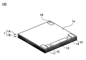
- FIG. 1 is a perspective view showing a piezoelectric element 100 according to a first embodiment of the present invention.
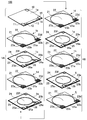
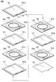
- 1 is an exploded perspective view of a piezoelectric element 100 according to a first embodiment of the present invention.
- FIGS. 3A and 3B are explanatory views showing a polarization process in manufacturing the piezoelectric element 100 according to the first embodiment of the present invention, respectively.
- FIG. 3B is a diagram illustrating FIG. The one-dot chain line SS part is shown.
- FIG. 4A is a perspective view showing a piezoelectric pump 200 that is a piezoelectric device according to the first embodiment of the present invention using the piezoelectric element 100 shown in FIGS. 1 to 3 as a drive source.
- FIG. 4B is a cross-sectional view showing the piezoelectric pump 200, and shows a dashed-dotted line TT portion in FIG.
- FIG. 5A is a partial plan view showing a connection portion between the first terminal 11 and the second terminal 12 and the metal terminal member 41 in the piezoelectric pump 200 according to the first embodiment of the present invention.
- FIGS. 5B and 5C are modifications. 6 (A) to 6 (C) are explanatory views showing the usage state of the piezoelectric pump 200 according to the first embodiment of the present invention, respectively, and FIGS. 6 (B) and 6 (C) are FIG. 6 (A).
- the piezoelectric element 100 concerning the dashed-dotted line UU part is shown.
- FIG. 6 is a perspective view showing a conventional piezoelectric element 400.
- FIG. 6 is an exploded perspective view of a conventional piezoelectric element 400.
- 12 (A) and 12 (B) are explanatory views showing a polarization process in manufacturing the conventional piezoelectric element 400, respectively, and
- FIG. 12 (B) is a one-dot chain line XX portion of FIG. 12 (A). Indicates.
- FIG. 13A is a perspective view showing a conventional piezoelectric pump 500 using the conventional piezoelectric element 400 shown in FIGS. 10 to 12 as a drive source.
- FIG. 13B is a cross-sectional view showing a conventional piezoelectric pump 500, and shows a dot-dash line YY portion in FIG. 14 (A) to 14 (C) are explanatory views showing the usage state of the conventional piezoelectric pump 500, respectively, and FIGS. 14 (B) and 14 (C) are the one-dot chain line ZZ portion of FIG. 14 (A).
- the piezoelectric element 400 concerning is shown.
- FIG. 1 and 2 show a piezoelectric element 100 according to a first embodiment of the present invention. 1 is a perspective view, and FIG. 2 is an exploded perspective view.
- the piezoelectric element 100 includes a piezoelectric body 1 in which a plurality of piezoelectric layers 1a to 1j are stacked.
- piezoelectric body 1 for example, piezoelectric ceramics mainly composed of lead zirconate titanate can be used.
- the first terminal 11, the second terminal 12, the third terminal 13, the fourth terminal 14, and the fifth terminal 15 are formed side by side on the surface of the piezoelectric body 1, that is, the surface of the piezoelectric layer 1 a laminated on the uppermost layer. Has been. Further, a dummy terminal 16 is formed in a portion away from these terminals.
- the first terminal 11, the second terminal 12, the third terminal 13, the fourth terminal 14, the fifth terminal 15, and the dummy terminal 16 are each filled with a conductive substance in a hole formed through the piezoelectric layer 1 a. It is connected to the inside of the piezoelectric body 1 through the filled via formed in this way.
- connection in order to increase the connection reliability at each connection portion, the connection is made using two filled vias.
- connection portions may be connected using one filling via.
- a slightly larger circular ground electrode 21 is formed at the center of the surface of the next piezoelectric layer 1b, and an annular dummy electrode 22 is formed around it.
- the ground electrode 21 has a lead electrode 21a formed along one side of the piezoelectric layer 1b. Further, along one side of the piezoelectric layer 1b, the relay electrodes 23a and 23b are adjacent to one side of the extraction electrode 21a, and the relay electrodes 23c and 23d are adjacent to the other side of the extraction electrode 21a. Is formed.
- the relay electrode 23a is connected to the first terminal 11, the relay electrode 23b is connected to the second terminal 12, the extraction electrode 21a is connected to the third terminal 13, and the relay electrode 23c is connected via the filling via formed in the piezoelectric layer 1a.
- the relay electrode 23d is connected to the fifth terminal 15 and the dummy electrode 22 is connected to the dummy terminal 16 to the fourth terminal 14, respectively.
- a circular center electrode 24 is formed at the center, and an annular peripheral electrode 25 is formed around it.
- the center electrode 24 has a lead electrode 24a formed along one side of the piezoelectric layer 1c.
- the peripheral electrode 25 is formed with two lead electrodes 25a and 25b along the same side where the lead electrode 24a of the piezoelectric layer 1c is formed, with the lead electrode 24a interposed therebetween.
- a ground relay electrode 26 is formed between the extraction electrode 24a and the extraction electrode 25a.
- a relay electrode 23e is formed adjacent to the lead electrode 25a on the side opposite to the ground relay electrode 26.
- the relay electrode 23e, the lead electrode 25a, the ground relay electrode 26, the lead electrode 24a, and the lead electrode 25b are sequentially formed on one side of the piezoelectric layer 1c. Further, a relay electrode 23f is formed on the surface of the piezoelectric layer 1c on a portion diagonal to the portion where the relay electrode 23e is formed. Then, via the filling via formed in the piezoelectric layer 1b, the relay electrode 23e is connected to the relay electrode 23a, the extraction electrode 25a is connected to the relay electrode 23b, the ground relay electrode 26 is connected to the extraction electrode 21a, and the extraction electrode 24a is connected to the relay electrode. 23c, the lead electrode 25b is connected to the relay electrode 23d, and the relay electrode 23f is connected to the dummy electrode 22.
- the next piezoelectric layer 1d has the same electrode pattern as that of the piezoelectric layer 1b described above.
- a ground electrode 21, a lead electrode 21a, a dummy electrode 22, relay electrodes 23a, 23b, 23c and 23d are formed on the surface of the piezoelectric layer 1d.
- the relay electrode 23a is connected to the relay electrode 23e
- the relay electrode 23b is connected to the extraction electrode 25a
- the extraction electrode 21a is connected to the ground relay electrode 26
- the relay electrode 23c is connected to the extraction electrode.
- the relay electrode 23d is connected to the extraction electrode 25b
- the dummy electrode 22 is connected to the relay electrode 23f.
- the next piezoelectric layer 1e has the same electrode pattern as that of the piezoelectric layer 1c described above.
- the center electrode 24, the extraction electrode 24a, the peripheral electrode 25, the extraction electrodes 25a, 25b, A ground relay electrode 26 and relay electrodes 23e and 23f are respectively formed.
- the relay electrode 23e is connected to the relay electrode 23a
- the extraction electrode 25a is connected to the relay electrode 23b
- the ground relay electrode 26 is connected to the extraction electrode 21a
- the extraction electrode 24a is connected to the relay electrode.
- the lead electrode 25b is connected to the relay electrode 23d
- the relay electrode 23f is connected to the dummy electrode 22.
- the next piezoelectric layer 1f has the same electrode pattern as that of the piezoelectric layers 1b and 1d described above.
- the ground electrode 21, the extraction electrode 21a, the dummy electrode 22, the relay electrode 23a, 23b, 23c, and 23d are formed on the surface of the piezoelectric layer 1f.
- the relay electrode 23a is connected to the relay electrode 23e
- the relay electrode 23b is connected to the lead electrode 25a
- the lead electrode 21a is connected to the ground relay electrode 26
- the relay electrode 23c is connected to the lead electrode via the filling via formed in the piezoelectric layer 1e.
- the relay electrode 23d is connected to the extraction electrode 25b
- the dummy electrode 22 is connected to the relay electrode 23f.
- the central electrode 24, the extraction electrode 24a, the peripheral electrode 25, the extraction electrodes 25a and 25b, the ground relay electrode 26, and the relay electrode are provided as in the piezoelectric layers 1c and 1e described above.
- 23e and 23f are formed, respectively, but the arrangement of the electrodes is different from that of the piezoelectric layers 1c and 1e (the formation order is different). That is, on one side of the piezoelectric layer 1g, the extraction electrode 25a, the extraction electrode 24a, the ground relay electrode 26, the extraction electrode 25b, and the relay electrode 23e are sequentially formed.
- the extraction electrode 25a is connected to the relay electrode 23a
- the extraction electrode 24a is connected to the relay electrode 23b
- the ground relay electrode 26 is connected to the extraction electrode 21a
- the extraction electrode 25d is connected to the relay electrode.
- the relay electrode 23e is connected to the relay electrode 23d
- the relay electrode 23f is connected to the dummy electrode 22, respectively.
- the next piezoelectric layer 1h has the same electrode pattern as the piezoelectric layers 1b, 1d, and 1f described above, and a ground electrode 21, a lead electrode 21a, a dummy electrode 22, and a relay electrode are formed on the surface of the piezoelectric layer 1h. 23a, 23b, 23c, and 23d are formed, respectively. Then, via the filling via formed in the piezoelectric layer 1g, the relay electrode 23a is the lead electrode 25a, the relay electrode 23b is the lead electrode 24a, the lead electrode 21a is the ground relay electrode 26, and the relay electrode 23c is the lead electrode. The relay electrode 23d is connected to the relay electrode 23e, and the dummy electrode 22 is connected to the relay electrode 23f.
- the next piezoelectric layer 1i has the same electrode pattern as that of the piezoelectric layer 1g described above.
- the center electrode 24, the extraction electrode 24a, the peripheral electrode 25, the extraction electrodes 25a, 25b, A ground relay electrode 26 and relay electrodes 23e and 23f are respectively formed.
- the extraction electrode 25a is connected to the relay electrode 23a
- the extraction electrode 24a is connected to the relay electrode 23b
- the ground relay electrode 26 is connected to the extraction electrode 21a
- the extraction electrode 25b is connected to the relay electrode.
- the relay electrode 23e is connected to the relay electrode 23d
- the relay electrode 23f is connected to the dummy electrode 22, respectively.
- the next piezoelectric layer 1j has the same electrode pattern as the above-described piezoelectric layers 1b, 1d, 1f, and 1h, and the surface of the piezoelectric layer 1j has a ground electrode 21, a lead electrode 21a, a dummy electrode 22, Relay electrodes 23a, 23b, 23c, and 23d are formed, respectively.
- the relay electrode 23a is the lead electrode 25a
- the relay electrode 23b is the lead electrode 24a
- the lead electrode 21a is the ground relay electrode 26
- the relay electrode 23c is the lead electrode.
- the relay electrode 23d is connected to the relay electrode 23e
- the dummy electrode 22 is connected to the relay electrode 23f.
- the piezoelectric body 1 has the first portion 1A (piezoelectric layers 1a to 1a) in the upper half with the interlayer surface between the piezoelectric layers 1e and 1f being the center in the stacking direction of the piezoelectric layers 1a to 1j.
- the central electrode 24 formed in 1e) and the peripheral electrode 25 formed in the second portion 1B (piezoelectric layers 1f to 1j) of the lower half are connected to the first terminal 11 and the fourth terminal 14. Is done.
- the peripheral electrode 25 formed on the first portion 1A and the center electrode 24 formed on the second portion 1B are connected to the second terminal 12 and the fifth terminal 15. All the ground electrodes 21 formed on the piezoelectric body 1 are connected to the third terminal 13. Further, all the dummy electrodes 22 formed on the piezoelectric body 1 are connected to the dummy terminals 16.
- center electrode 24 formed in the first portion 1A and the peripheral electrode 25 formed in the second portion 1B are replaced with the second terminal 12 and the fifth terminal 15 by changing the way of extracting each electrode.
- peripheral electrode 25 formed on the first portion 1A and the central electrode 24 formed on the second portion 1B are connected to the first terminal 11 and the fourth terminal 14. Good.
- the piezoelectric body 1 having such a structure has, for example, a conductive paste applied on the surface thereof, and necessary terminals (first terminal 11, second terminal 12, third terminal 13, fourth terminal 14, fifth terminal 15, dummy).
- Terminal 16 necessary electrodes (ground electrode 21, lead electrode 21a, dummy electrode 22, center electrode 24, lead electrode 24a, relay electrodes 23a, 23b, 23c, 23d, 23e, 23f, peripheral electrode 25, lead electrode 25a, 25b, a ground relay electrode 26), and a piezoelectric green for forming the piezoelectric layers 1a to 1j in which holes formed therethrough are filled with a conductive paste and necessary filling vias are formed. Sheets are prepared, these are laminated, pressed, and fired with a predetermined profile.
- FIG. 3 (A) and 3 (B) are explanatory views showing a polarization process of the piezoelectric element 100, and FIG. 3 (B) shows an alternate long and short dash line SS part of FIG. 3 (A).
- the height direction is enlarged with respect to the width direction in order to easily show the polarization direction.
- a positive voltage is applied to the first terminal 11 and the fourth terminal 14, and the second terminal. 12.
- a negative voltage is applied to the fifth terminal 15.
- the positive voltage is selected from a range of 30 V to 50 V, for example, and the negative voltage is selected from a range of ⁇ 50 V to ⁇ 30 V, for example, and the application time is, for example, 1 second to 120 seconds.
- the dummy terminal 16 is not used for the polarization process.
- the positive voltage and the negative voltage to be applied may be reversed, and the negative voltage may be applied to the first terminal 11 and the fourth terminal 14, and the positive voltage may be applied to the second terminal 12 and the fifth terminal 15.
- the piezoelectric layers 1b to 1i constituting the piezoelectric element 1 are polarized in the directions indicated by the arrows in the drawing.
- the uppermost piezoelectric layer 1a and the lowermost piezoelectric layer 1j are not polarized.
- the polarization directions of the piezoelectric layers 1b to 1i are reversed in the central portion and the peripheral portion.
- the center electrode 24 formed on the first portion 1A and the peripheral electrode 25 formed on the second portion 1B are connected to the first terminal 11 and the fourth terminal 14 and formed on the first portion 1A. Since the peripheral electrode 25 and the center electrode 24 formed on the second portion 1B are connected to the second terminal 12 and the fifth terminal 15, the piezoelectric layers 1b to 1e of the first portion 1A, In the piezoelectric layers 1f to 1i of the second portion 1B, the polarization repetition order is different.
- the piezoelectric element 100 having such a structure and polarized is used as a drive source of a piezoelectric device such as a piezoelectric pump, for example.
- 4A and 4B show a piezoelectric pump 200 according to the first embodiment of the present invention using the piezoelectric element 100 as a drive source.
- 4A is a perspective view
- FIG. 4B is a cross-sectional view
- FIG. 4B shows a dashed-dotted line TT portion in FIG. 4A.
- the piezoelectric pump 200 includes a pump body 31.
- the pump body 31 is formed with a hollow pump chamber 31a, an opening 31b opened above the pump chamber 31a, and two holes 31c and 31d connected to the pump chamber 31a.
- the opening 31b is closed by the diaphragm 32, and the piezoelectric element 100 is bonded and fixed to the diaphragm 32.
- an inflow check valve 33 is attached to the hole 31c, and an outflow check valve 34 is attached to the hole 31d.
- the check valve 33 on the inflow side functions to allow the inflow of fluid from the outside to the pump chamber 31a but to prevent the outflow in the reverse direction.
- the check valve 34 on the outflow side allows fluid to flow out from the pump chamber 31a to the outside, but functions to prevent inflow in the reverse direction.
- metal terminal members 41 and 42 are fixed to the upper surface of the pump main body 31.
- the metal terminal member 41 is connected to the first terminal 11 and the second terminal 12 of the piezoelectric element 100, and the metal terminal member 42 is connected to the third terminal 13 by a bonding material such as conductive paste and solder.
- the metal terminal member is not connected to the fourth terminal 14 and the fifth terminal 15. (In FIG. 4A, illustration of the bonding material is omitted.)
- FIG. 5A shows a connection state between the metal terminal member 41 and the first terminal 11 and the second terminal 12.
- the metal terminal member 41 is in partial contact with both the first terminal 11 and the second terminal 12. At this time, it is preferable that the metal terminal member 41 does not contact a portion where the filling vias (shown by black dots in the drawing) of the first terminal 11 and the second terminal 12 are formed. This is to prevent the filled via, the piezoelectric body 1 and the like from being damaged or damaged due to the metal terminal member 41 coming into contact with the filled via.
- a bonding material such as a conductive paste is applied to a portion surrounded by a chain line, and the first terminal 11 and the second terminal 12 and the metal terminal member 41 are connected.
- FIG. 5 (B) and 5 (C) show a modification of the connection between the first terminal 11 and the second terminal 12 and the metal terminal member 41.
- FIG. 5B the metal terminal member 41 is in contact with only one terminal, for example, the second terminal 12, and is connected to the first terminal 11 which is the other terminal with a bonding material. You may do it.
- FIG. 5C the metal terminal member 41 should not be in contact with both of the terminals, the first terminal 11 and the second terminal 12, and should be connected with a bonding material. Also good.
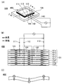
- FIGS. 6A to 6C show the driving state of the piezoelectric pump 200.
- FIG. FIGS. 6A to 6C are explanatory diagrams, respectively, and FIGS. 6B and 6C show a dot-dash line U-U portion of the piezoelectric element 100 of FIG. 6A.
- the height direction is enlarged with respect to the width direction in order to easily show the expansion and contraction of the piezoelectric layers 1a to 1j constituting the piezoelectric element 100.
- one terminal of an AC power source that is a driving power source is connected to a third terminal via a metal terminal member 42. 13, and the other terminal of the AC power supply is connected to the first terminal 11 and the second terminal 12 via the metal terminal member 41.
- the AC power source for example, an AC power source that generates an AC of 1V to 20V is used.
- the AC power supply is not limited to one that generates a sine wave, and may be one that generates a rectangular wave or the like.
- the piezoelectric layers 1a to 1j constituting the piezoelectric body 1 of the piezoelectric element 100 are polarized as shown in FIG. 3B (however, the uppermost piezoelectric layer 1a and the lowermost piezoelectric layer 1j are Not polarized). For this reason, when alternating current is applied, for example, as shown by the arrow in FIG. For example, at this time, the central portion of the piezoelectric layers 1b to 1e contracts, and the peripheral portion around the central portion expands. On the other hand, the central part of the piezoelectric layers 1f to 1i expands, and the peripheral part around it contracts. As a result, as shown by the hatched arrow in FIG. 6C, the piezoelectric element 100 is bent and displaced at the center part in the downward direction and bent at the peripheral part in the upward direction.
- the piezoelectric element 100 When the polarity of the AC power supply changes, the piezoelectric element 100 exhibits the opposite behavior to that shown in FIGS. 6 (B) and 6 (C). That is, the central part of the piezoelectric layers 1b to 1e expands, the peripheral part around it contracts, the central part of the piezoelectric layers 1f to 1i contracts, and the peripheral part around it extends.
- the piezoelectric element 100 is bent and displaced in the center at the center and bent and displaced at the periphery in the downward direction.
- the piezoelectric pump 200 shown in FIGS. 4A and 4B has a fluid flowing into the pump chamber 31a from the hole 31c.
- the fluid that has flowed into the chamber 31a flows out from the hole 31d.
- the piezoelectric body 1 is formed by multilayering the piezoelectric layers 1a to 1j, and the piezoelectric layers 1b to 1i are polarized in opposite directions in the central portion and the peripheral portion. Therefore, it can be driven at a relatively low voltage, and a large amount of displacement can be obtained at the center of the piezoelectric element 100. Therefore, the piezoelectric pump 200 according to the present embodiment using the piezoelectric element 100 as a drive source functions efficiently with small power consumption. In addition, since the same potential is always applied to the center electrode 24 and the peripheral electrode 25 formed in the same layer, electromigration does not occur between them, and there is no short circuit between them.
- the piezoelectric element 100 can be driven simply by connecting the two metal terminal members 41 and 42, and it is not necessary to connect the three metal terminal members as in the prior art, so that the mounting is easy. Further, the piezoelectric pump 200 using the piezoelectric element 100 as a drive source has improved design freedom and is easy to manufacture.
- the piezoelectric element 100 according to the first embodiment and the piezoelectric pump 200 using the piezoelectric element 100 as a drive source have been described above.
- the present invention is not limited to the above contents, and various modifications can be made in accordance with the gist of the invention.
- the first portion 1A is composed of five layers of piezoelectric layers 1a to 1e
- the second portion 1B is composed of five layers of piezoelectric layers 1f to 1j.
- the number of layers is not limited to these, and the number of layers can be increased or decreased.
- the piezoelectric layer 1b and the piezoelectric layer 1c may be combined, and a desired number of combinations may be added, for example, below the piezoelectric layer 1a.
- the piezoelectric layer 1f and the piezoelectric layer 1g may be combined, and a desired number of combinations may be added below the piezoelectric layer 1e, for example.
- the filling vias are at the same position when seen through in the stacking direction. Instead of overlapping, they may be formed shifted from each other as shown in FIG. In this case, it is possible to prevent the deformation of the piezoelectric body 1 due to the filling via being continuously formed in the stacking direction.
- the same shape is not laminated vertically, but as shown in FIG. 8A, for example, a rectangular relay electrode 23g, a circular relay is formed.
- the electrode 23h, the rectangular relay electrode 23i, and the circular relay electrode 23j are stacked, or as shown in FIG. 8B, a relay electrode 23k having a certain shape, for example, a rectangular one rotated by a certain angle.
- relay electrodes 23o to 23r in which a certain shape, for example, a rectangular shape is shifted in the horizontal direction may be stacked as shown in FIG. 8C. In this case, it is possible to prevent the steps generated by forming each relay electrode from accumulating at the same position and preventing a large step from occurring on the surface of the piezoelectric body. The deformation of the piezoelectric body can be prevented.
- the piezoelectric pump 200 connects one terminal of an AC power source that is a driving power source to the third terminal 13, and the other terminal of the AC power source.
- the terminals are connected to the first terminal 11 and the second terminal 12, but the other terminal of the AC power supply is connected to the fourth terminal 14 and the fifth terminal 15 instead of the first terminal 11 and the second terminal 12. You may make it do.
- the piezoelectric device using the piezoelectric element 100 as a drive source is not limited to the piezoelectric pump, and may be a piezoelectric blower or a piezoelectric fan.
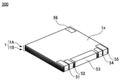
- FIG. 9 shows a piezoelectric element 300 according to the second embodiment of the present invention. However, FIG. 9 is a perspective view.
- electrical connection between layers is performed inside the piezoelectric body 1 through filling vias formed in the piezoelectric layers 1a to 1i (see FIGS. 1 and 2). ).
- the piezoelectric element 300 according to the second embodiment as shown in FIG. 9, the first terminal 51, the second terminal 52, The electrical connection between the layers is performed via the 3 terminal 53, the fourth terminal 54, the fifth terminal 55, and the dummy terminal 56. Accordingly, although not shown, the ground connection electrode, the relay electrode, and the extraction electrode formed on each piezoelectric layer are formed so as to be in contact with the sides of each piezoelectric layer.
- Other configurations of the piezoelectric element 300 according to the second embodiment are the same as those of the piezoelectric element 100 according to the first embodiment.
- the electrical connection between the layers can be performed via the terminal formed on the side surface of the piezoelectric body 1 instead of the filling via.
- Piezoelectric bodies 1a to 1j Piezoelectric layer 11, 51: First terminal 12, 52: Second terminal 13, 53: Third terminal 14, 54: Fourth terminal 15, 55: Fifth terminal 21: Ground electrode 21a: extraction electrode 22: dummy electrodes 23a to 23r: relay electrode 24: center electrode 24a: extraction electrode 25: peripheral electrode 25a: extraction electrode 26: ground relay electrode 31: pump body 31a: pump chamber 31b: openings 31c, 31d: Hole 32: Diaphragm 33, 34: Check valve 41, 42: Metal terminal member 100, 300: Piezoelectric element 200: Piezoelectric pump (piezoelectric device)
Landscapes
- Engineering & Computer Science (AREA)
- Mechanical Engineering (AREA)
- General Engineering & Computer Science (AREA)
- Reciprocating Pumps (AREA)
- General Electrical Machinery Utilizing Piezoelectricity, Electrostriction Or Magnetostriction (AREA)
Priority Applications (4)
| Application Number | Priority Date | Filing Date | Title |
|---|---|---|---|
| JP2013502228A JP5500308B2 (ja) | 2011-03-01 | 2012-02-10 | 圧電素子およびこれを用いた圧電装置 |
| CN201280010524.8A CN103392244B (zh) | 2011-03-01 | 2012-02-10 | 压电元件以及使用该压电元件的压电装置 |
| EP12752085.6A EP2682995A4 (de) | 2011-03-01 | 2012-02-10 | Piezoelektrisches element und piezoelektrische vorrichtung damit |
| US13/969,759 US9406861B2 (en) | 2011-03-01 | 2013-08-19 | Piezoelectric element and piezoelectric device using the same |
Applications Claiming Priority (2)
| Application Number | Priority Date | Filing Date | Title |
|---|---|---|---|
| JP2011-043847 | 2011-03-01 | ||
| JP2011043847 | 2011-03-01 |
Related Child Applications (1)
| Application Number | Title | Priority Date | Filing Date |
|---|---|---|---|
| US13/969,759 Continuation US9406861B2 (en) | 2011-03-01 | 2013-08-19 | Piezoelectric element and piezoelectric device using the same |
Publications (1)
| Publication Number | Publication Date |
|---|---|
| WO2012117831A1 true WO2012117831A1 (ja) | 2012-09-07 |
Family
ID=46757770
Family Applications (1)
| Application Number | Title | Priority Date | Filing Date |
|---|---|---|---|
| PCT/JP2012/053147 Ceased WO2012117831A1 (ja) | 2011-03-01 | 2012-02-10 | 圧電素子およびこれを用いた圧電装置 |
Country Status (5)
| Country | Link |
|---|---|
| US (1) | US9406861B2 (de) |
| EP (1) | EP2682995A4 (de) |
| JP (1) | JP5500308B2 (de) |
| CN (1) | CN103392244B (de) |
| WO (1) | WO2012117831A1 (de) |
Cited By (6)
| Publication number | Priority date | Publication date | Assignee | Title |
|---|---|---|---|---|
| CN103795370A (zh) * | 2012-10-30 | 2014-05-14 | 太阳诱电株式会社 | 电子元件模块 |
| WO2015114849A1 (ja) * | 2014-01-30 | 2015-08-06 | 京セラ株式会社 | 圧電素子およびこれを備えた圧電振動装置、携帯端末、音響発生器、音響発生装置、電子機器 |
| JP2017103293A (ja) * | 2015-11-30 | 2017-06-08 | Tdk株式会社 | 圧電素子及び圧電アクチュエータ |
| US10686119B2 (en) | 2016-06-08 | 2020-06-16 | Tdk Corporation | Piezoelectric device |
| JP2024034326A (ja) * | 2022-08-31 | 2024-03-13 | Tdk株式会社 | 圧電素子 |
| US11952994B2 (en) * | 2017-12-22 | 2024-04-09 | Murata Manufacturing Co., Ltd. | Piezoelectric pump housing and terminal arrangement |
Families Citing this family (3)
| Publication number | Priority date | Publication date | Assignee | Title |
|---|---|---|---|---|
| DE102012111972A1 (de) * | 2012-12-07 | 2014-06-12 | Epcos Ag | Verfahren zur Herstellung eines elektronischen Bauteils |
| US10618551B2 (en) * | 2016-02-01 | 2020-04-14 | Ford Global Technologies, Llc | Clearance and preload adjustment for steering mechanism using piezoelectric elements |
| WO2017179616A1 (ja) * | 2016-04-15 | 2017-10-19 | 第一精工株式会社 | スピーカシステム |
Citations (3)
| Publication number | Priority date | Publication date | Assignee | Title |
|---|---|---|---|---|
| JPH03171784A (ja) * | 1989-11-30 | 1991-07-25 | Toshiba Corp | バイモルフ素子 |
| WO2008007634A1 (en) | 2006-07-11 | 2008-01-17 | Murata Manufacturing Co., Ltd. | Piezoelectric pump |
| WO2009072434A1 (ja) * | 2007-12-03 | 2009-06-11 | Murata Manufacturing Co., Ltd. | 圧電ポンプ |
Family Cites Families (18)
| Publication number | Priority date | Publication date | Assignee | Title |
|---|---|---|---|---|
| US4257686A (en) * | 1978-12-14 | 1981-03-24 | Itek Corporation | Multiple layer piezoelectric wavefront modulator |
| JP3402256B2 (ja) * | 1999-05-25 | 2003-05-06 | 株式会社村田製作所 | 積層型圧電部品 |
| AU4056799A (en) * | 1999-05-31 | 2000-12-18 | Nanomotion Ltd. | Multilayer piezoelectric motor |
| US6933657B2 (en) * | 2001-03-30 | 2005-08-23 | Canon Kabushiki Kaisha | Stacked electro-mechanical energy conversion element and method of manufacturing the same |
| JP4511120B2 (ja) * | 2002-04-03 | 2010-07-28 | オリンパス株式会社 | 超音波リニアモータ |
| WO2005067070A1 (de) * | 2004-01-12 | 2005-07-21 | Siemens Aktiengesellschaft | Aktor mit innenliegender anschlusselektrode und herstellungsverfahren für einen solchen aktor |
| WO2005104639A1 (ja) * | 2004-04-20 | 2005-11-03 | Murata Manufacturing Co., Ltd. | 多層セラミック基板およびその製造方法ならびに圧電共振部品 |
| JP2006004980A (ja) * | 2004-06-15 | 2006-01-05 | Canon Inc | 積層電気−機械エネルギー変換素子及び振動波駆動装置 |
| JP4576185B2 (ja) * | 2004-09-22 | 2010-11-04 | オリンパス株式会社 | 超音波振動子 |
| JP2006157172A (ja) * | 2004-11-25 | 2006-06-15 | Murata Mfg Co Ltd | 圧電フィルタ装置 |
| KR100691280B1 (ko) * | 2005-09-05 | 2007-03-12 | 삼성전기주식회사 | 압전 진동자, 그 제조방법 및 압전 진동자를 구비하는 선형액추에이터 |
| CN101213733B (zh) * | 2006-01-23 | 2011-03-02 | 松下电器产业株式会社 | 压电元件与超声波执行机构 |
| JP5234008B2 (ja) * | 2008-04-17 | 2013-07-10 | 株式会社村田製作所 | 積層型圧電素子及び圧電ポンプ |
| US7932661B2 (en) * | 2008-09-23 | 2011-04-26 | Nikko Company | Piezoelectric vibrator for ultrasonic motor |
| AU2009335654A1 (en) * | 2008-12-18 | 2011-06-30 | Discovery Technology International, Inc. | Piezoelectric quasi-resonance motors based on acoustic standing waves with combined resonator |
| JP5429140B2 (ja) * | 2010-01-19 | 2014-02-26 | Tdk株式会社 | 圧電アクチュエータ |
| KR20130104338A (ko) * | 2012-03-13 | 2013-09-25 | 삼성전기주식회사 | 적층 세라믹 전자부품 및 그 제조방법 |
| US9579691B2 (en) * | 2013-05-21 | 2017-02-28 | Mplus Co., Ltd. | Piezoelectric element and electronic component including the same |
-
2012
- 2012-02-10 EP EP12752085.6A patent/EP2682995A4/de not_active Withdrawn
- 2012-02-10 JP JP2013502228A patent/JP5500308B2/ja active Active
- 2012-02-10 WO PCT/JP2012/053147 patent/WO2012117831A1/ja not_active Ceased
- 2012-02-10 CN CN201280010524.8A patent/CN103392244B/zh active Active
-
2013
- 2013-08-19 US US13/969,759 patent/US9406861B2/en active Active
Patent Citations (3)
| Publication number | Priority date | Publication date | Assignee | Title |
|---|---|---|---|---|
| JPH03171784A (ja) * | 1989-11-30 | 1991-07-25 | Toshiba Corp | バイモルフ素子 |
| WO2008007634A1 (en) | 2006-07-11 | 2008-01-17 | Murata Manufacturing Co., Ltd. | Piezoelectric pump |
| WO2009072434A1 (ja) * | 2007-12-03 | 2009-06-11 | Murata Manufacturing Co., Ltd. | 圧電ポンプ |
Non-Patent Citations (1)
| Title |
|---|
| See also references of EP2682995A4 |
Cited By (8)
| Publication number | Priority date | Publication date | Assignee | Title |
|---|---|---|---|---|
| CN103795370A (zh) * | 2012-10-30 | 2014-05-14 | 太阳诱电株式会社 | 电子元件模块 |
| WO2015114849A1 (ja) * | 2014-01-30 | 2015-08-06 | 京セラ株式会社 | 圧電素子およびこれを備えた圧電振動装置、携帯端末、音響発生器、音響発生装置、電子機器 |
| JPWO2015114849A1 (ja) * | 2014-01-30 | 2017-03-23 | 京セラ株式会社 | 圧電素子およびこれを備えた圧電振動装置、携帯端末、音響発生器、音響発生装置、電子機器 |
| US9813823B2 (en) | 2014-01-30 | 2017-11-07 | Kyocera Corporation | Piezoelectric element, and piezoelectric vibrating apparatus, portable terminal, sound generator, sound generating apparatus, and electronic device comprising the piezoelectric element |
| JP2017103293A (ja) * | 2015-11-30 | 2017-06-08 | Tdk株式会社 | 圧電素子及び圧電アクチュエータ |
| US10686119B2 (en) | 2016-06-08 | 2020-06-16 | Tdk Corporation | Piezoelectric device |
| US11952994B2 (en) * | 2017-12-22 | 2024-04-09 | Murata Manufacturing Co., Ltd. | Piezoelectric pump housing and terminal arrangement |
| JP2024034326A (ja) * | 2022-08-31 | 2024-03-13 | Tdk株式会社 | 圧電素子 |
Also Published As
| Publication number | Publication date |
|---|---|
| CN103392244B (zh) | 2016-01-20 |
| EP2682995A1 (de) | 2014-01-08 |
| US9406861B2 (en) | 2016-08-02 |
| CN103392244A (zh) | 2013-11-13 |
| EP2682995A4 (de) | 2014-10-22 |
| JP5500308B2 (ja) | 2014-05-21 |
| US20130334933A1 (en) | 2013-12-19 |
| JPWO2012117831A1 (ja) | 2014-07-07 |
Similar Documents
| Publication | Publication Date | Title |
|---|---|---|
| JP5500308B2 (ja) | 圧電素子およびこれを用いた圧電装置 | |
| JP5234008B2 (ja) | 積層型圧電素子及び圧電ポンプ | |
| JP6479896B2 (ja) | 多層コンデンサおよび多層コンデンサの製造方法 | |
| JP2016051895A (ja) | 圧電素子及びこれを含む圧電振動モジュール | |
| JP2016175274A5 (de) | ||
| JP4185486B2 (ja) | 積層型圧電素子 | |
| JP4720068B2 (ja) | 積層型圧電素子 | |
| JP2012504858A (ja) | 外部電極を有する圧電アクチュエータ | |
| JP4343552B2 (ja) | 積層圧電素子 | |
| JP5821536B2 (ja) | 積層型圧電素子 | |
| JP4506172B2 (ja) | 積層型圧電素子 | |
| JP5561247B2 (ja) | 圧電素子 | |
| JP4057520B2 (ja) | 電子部品 | |
| JP2013012657A (ja) | 圧電素子 | |
| JP2012138505A (ja) | 圧電アクチュエータ | |
| JP4586352B2 (ja) | 積層型圧電素子 | |
| JP5087822B2 (ja) | 圧電素子 | |
| JP4529427B2 (ja) | 積層型圧電素子 | |
| JP6011325B2 (ja) | アクチュエータ、セル基板複合体、セル基板複合体の製造方法及びアクチュエータの製造方法 | |
| JP2006147941A (ja) | 積層型セラミック素子 | |
| JP5768229B2 (ja) | 圧電素子およびその製造方法 | |
| JP5747685B2 (ja) | 圧電素子 | |
| JP2008300438A (ja) | 積層型圧電素子ならびにその製造方法 | |
| JP2014194975A (ja) | 二重螺旋積層型圧電アクチュエータ及びその製造方法 | |
| JP2006147940A (ja) | 積層型セラミック素子 |
Legal Events
| Date | Code | Title | Description |
|---|---|---|---|
| 121 | Ep: the epo has been informed by wipo that ep was designated in this application |
Ref document number: 12752085 Country of ref document: EP Kind code of ref document: A1 |
|
| ENP | Entry into the national phase |
Ref document number: 2013502228 Country of ref document: JP Kind code of ref document: A |
|
| WWE | Wipo information: entry into national phase |
Ref document number: 2012752085 Country of ref document: EP |
|
| NENP | Non-entry into the national phase |
Ref country code: DE |