EP2682995A1 - Piezoelektrisches element und piezoelektrische vorrichtung damit - Google Patents
Piezoelektrisches element und piezoelektrische vorrichtung damit Download PDFInfo
- Publication number
- EP2682995A1 EP2682995A1 EP12752085.6A EP12752085A EP2682995A1 EP 2682995 A1 EP2682995 A1 EP 2682995A1 EP 12752085 A EP12752085 A EP 12752085A EP 2682995 A1 EP2682995 A1 EP 2682995A1
- Authority
- EP
- European Patent Office
- Prior art keywords
- terminal
- piezoelectric
- electrodes
- layers
- electrode
- Prior art date
- Legal status (The legal status is an assumption and is not a legal conclusion. Google has not performed a legal analysis and makes no representation as to the accuracy of the status listed.)
- Withdrawn
Links
- 230000002093 peripheral effect Effects 0.000 claims abstract description 62
- 239000010410 layer Substances 0.000 claims description 153
- 239000002184 metal Substances 0.000 claims description 28
- 238000003475 lamination Methods 0.000 claims description 12
- 239000011229 interlayer Substances 0.000 claims description 3
- 239000000126 substance Substances 0.000 claims description 3
- 238000000605 extraction Methods 0.000 abstract description 69
- 238000006073 displacement reaction Methods 0.000 abstract description 5
- 230000010287 polarization Effects 0.000 description 15
- 239000012530 fluid Substances 0.000 description 12
- 230000015572 biosynthetic process Effects 0.000 description 8
- 238000010586 diagram Methods 0.000 description 8
- 238000000034 method Methods 0.000 description 8
- 239000000463 material Substances 0.000 description 7
- 238000004519 manufacturing process Methods 0.000 description 6
- 230000006399 behavior Effects 0.000 description 4
- 230000015556 catabolic process Effects 0.000 description 2
- 230000008602 contraction Effects 0.000 description 2
- 238000006731 degradation reaction Methods 0.000 description 2
- 238000010304 firing Methods 0.000 description 2
- 238000010030 laminating Methods 0.000 description 2
- 229910000679 solder Inorganic materials 0.000 description 2
- 239000000919 ceramic Substances 0.000 description 1
- 230000000694 effects Effects 0.000 description 1
Images





Classifications
-
- F—MECHANICAL ENGINEERING; LIGHTING; HEATING; WEAPONS; BLASTING
- F04—POSITIVE - DISPLACEMENT MACHINES FOR LIQUIDS; PUMPS FOR LIQUIDS OR ELASTIC FLUIDS
- F04B—POSITIVE-DISPLACEMENT MACHINES FOR LIQUIDS; PUMPS
- F04B43/00—Machines, pumps, or pumping installations having flexible working members
- F04B43/02—Machines, pumps, or pumping installations having flexible working members having plate-like flexible members, e.g. diaphragms
- F04B43/04—Pumps having electric drive
- F04B43/043—Micropumps
- F04B43/046—Micropumps with piezoelectric drive
-
- H—ELECTRICITY
- H10—SEMICONDUCTOR DEVICES; ELECTRIC SOLID-STATE DEVICES NOT OTHERWISE PROVIDED FOR
- H10N—ELECTRIC SOLID-STATE DEVICES NOT OTHERWISE PROVIDED FOR
- H10N30/00—Piezoelectric or electrostrictive devices
- H10N30/50—Piezoelectric or electrostrictive devices having a stacked or multilayer structure
-
- H—ELECTRICITY
- H10—SEMICONDUCTOR DEVICES; ELECTRIC SOLID-STATE DEVICES NOT OTHERWISE PROVIDED FOR
- H10N—ELECTRIC SOLID-STATE DEVICES NOT OTHERWISE PROVIDED FOR
- H10N30/00—Piezoelectric or electrostrictive devices
- H10N30/80—Constructional details
- H10N30/87—Electrodes or interconnections, e.g. leads or terminals
- H10N30/871—Single-layered electrodes of multilayer piezoelectric or electrostrictive devices, e.g. internal electrodes
-
- H—ELECTRICITY
- H10—SEMICONDUCTOR DEVICES; ELECTRIC SOLID-STATE DEVICES NOT OTHERWISE PROVIDED FOR
- H10N—ELECTRIC SOLID-STATE DEVICES NOT OTHERWISE PROVIDED FOR
- H10N30/00—Piezoelectric or electrostrictive devices
- H10N30/80—Constructional details
- H10N30/87—Electrodes or interconnections, e.g. leads or terminals
- H10N30/872—Interconnections, e.g. connection electrodes of multilayer piezoelectric or electrostrictive devices
-
- H—ELECTRICITY
- H10—SEMICONDUCTOR DEVICES; ELECTRIC SOLID-STATE DEVICES NOT OTHERWISE PROVIDED FOR
- H10N—ELECTRIC SOLID-STATE DEVICES NOT OTHERWISE PROVIDED FOR
- H10N30/00—Piezoelectric or electrostrictive devices
- H10N30/80—Constructional details
- H10N30/87—Electrodes or interconnections, e.g. leads or terminals
- H10N30/872—Interconnections, e.g. connection electrodes of multilayer piezoelectric or electrostrictive devices
- H10N30/874—Interconnections, e.g. connection electrodes of multilayer piezoelectric or electrostrictive devices embedded within piezoelectric or electrostrictive material, e.g. via connections
-
- H—ELECTRICITY
- H10—SEMICONDUCTOR DEVICES; ELECTRIC SOLID-STATE DEVICES NOT OTHERWISE PROVIDED FOR
- H10N—ELECTRIC SOLID-STATE DEVICES NOT OTHERWISE PROVIDED FOR
- H10N30/00—Piezoelectric or electrostrictive devices
- H10N30/80—Constructional details
- H10N30/87—Electrodes or interconnections, e.g. leads or terminals
- H10N30/875—Further connection or lead arrangements, e.g. flexible wiring boards, terminal pins
-
- H—ELECTRICITY
- H10—SEMICONDUCTOR DEVICES; ELECTRIC SOLID-STATE DEVICES NOT OTHERWISE PROVIDED FOR
- H10N—ELECTRIC SOLID-STATE DEVICES NOT OTHERWISE PROVIDED FOR
- H10N30/00—Piezoelectric or electrostrictive devices
- H10N30/20—Piezoelectric or electrostrictive devices with electrical input and mechanical output, e.g. functioning as actuators or vibrators
- H10N30/204—Piezoelectric or electrostrictive devices with electrical input and mechanical output, e.g. functioning as actuators or vibrators using bending displacement, e.g. unimorph, bimorph or multimorph cantilever or membrane benders
- H10N30/2047—Membrane type
Definitions
- the present invention relates to a piezoelectric element, and more specifically to a piezoelectric element which is easy to mount on or in a piezoelectric device such as a piezoelectric pump.
- the present invention further relates to a piezoelectric device using the piezoelectric element.
- a piezoelectric element has recently been used as a drive source of a small-sized, high-precision pump, blower, fan, or the like. Further, the piezoelectric element for this purpose is demanded to be capable of being driven with a relatively low voltage and obtaining a large displacement amount at a central portion of the piezoelectric element, and not to be degraded in characteristics over time.
- Figs. 10 and 11 illustrate a piezoelectric element 400 disclosed in Patent Document 1.
- Fig. 10 is a perspective view
- Fig. 11 is an exploded perspective view.
- the piezoelectric element 400 includes a piezoelectric body 101 having a plurality of laminated piezoelectric layers 101a to 101h.
- a first terminal 111, a second terminal 112, and a third terminal 113 are formed in a line on surfaces of the piezoelectric body 101.
- a rectangular ground electrode 121 is formed on a surface of the piezoelectric layer 101a forming the uppermost layer.
- the ground electrode 121 is extracted to the second terminal 112.
- a circular central electrode 124 is formed in a central portion of a surface of the next piezoelectric layer 101b, and a ring-shaped peripheral electrode 125 is formed therearound.
- the central electrode 124 is extracted to the third terminal 113, and the peripheral electrode 125 is extracted to the first terminal 111.
- a rectangular ground electrode 121 is formed on a surface of the next piezoelectric layer 101c.
- the ground electrode 121 is extracted to the second terminal 112.
- a circular central electrode 124 is formed in a central portion of a surface of the next piezoelectric layer 101d, and a ring-shaped peripheral electrode 125 is formed therearound.
- the central electrode 124 is extracted to the third terminal 113, and the peripheral electrode 125 is extracted to the first terminal 111.
- a rectangular ground electrode 121 is formed on a surface of the next piezoelectric layer 101e.
- the ground electrode 121 is extracted to the second terminal 112.
- a circular central electrode 124 is formed in a central portion of a surface of the next piezoelectric layer 101f, and a ring-shaped peripheral electrode 125 is formed therearound.
- the central electrode 124 is extracted to the first terminal 111, and the peripheral electrode 125 is extracted to the third terminal 113.
- a rectangular ground electrode 121 is formed on a surface of the next piezoelectric layer 101g.
- the ground electrode 121 is extracted to the second terminal 112.
- a circular central electrode 124 is formed in a central portion of a surface of the next piezoelectric layer 101h, and a ring-shaped peripheral electrode 125 is formed therearound.
- the central electrode 124 is extracted to the first terminal 111
- the peripheral electrode 125 is extracted to the third terminal 113.
- the rear surface of the piezoelectric layer 101h is formed with a rectangular ground electrode 121.
- the ground electrode 121 is extracted to the second terminal 112.
- the existing piezoelectric element 400 has the ground electrodes 121 exposed on both upper and lower surfaces thereof.
- the piezoelectric element 400 may be configured such that piezoelectric layers not formed with an electrode are laminated on both the upper and lower surfaces so as not to expose the ground electrodes 121.
- the piezoelectric body 101 having the above-described structure is formed by a method of, for example, laminating, compressing, and firing piezoelectric green sheets for forming the piezoelectric layers 101a to 101h, on which the necessary electrodes (the ground electrodes 121, the central electrodes 124, and the peripheral electrodes 125) are formed by conductive paste or the like. Further, the first terminal 111, the second terminal 112, and the third terminal 113 are formed by a method of, for example, baking conductive paste onto surfaces of the fired piezoelectric body 101.
- the piezoelectric element 400 is polarized by a direct-current voltage applied to the first terminal 111, the second terminal 112, and the third terminal 113.
- (A) and (B) of Fig. 12 are explanatory diagrams illustrating a polarization process of the piezoelectric element 400.
- (B) of Fig. 12 illustrates a portion of (A) of Fig. 12 indicated by a dash-dotted line X-X.
- the scale in the height direction is enlarged as compared with that in the width direction to clarify polarization directions.
- each of the piezoelectric layers 101a to 101h forming the piezoelectric element 400 is polarized in the directions indicated by arrows in the drawing.
- the polarization direction is opposite between a central portion and a peripheral portion.
- the repeating order of polarization is different between the piezoelectric layers 101a to 101d and the piezoelectric layers 101e to 101h.
- the piezoelectric element 400 having such a structure and subjected to polarization is used as, for example, a drive source of a piezoelectric device such as a piezoelectric pump.
- A) and (B) of Fig. 13 illustrate a piezoelectric pump 500 using the piezoelectric element 400 as a drive source thereof.
- (A) of Fig. 13 is a perspective view
- (B) of Fig. 13 is a cross-sectional view illustrating a portion of (A) of Fig. 13 indicated by a dash-dotted line Y-Y.
- the piezoelectric pump 500 includes a pump body 131.
- the pump body 131 is formed with a hollow pump chamber 131a, an opening 131b that opens an upper portion of the pump chamber 131a, and two holes 131c and 131d that communicate with the pump chamber 131a.
- the opening 131b is closed by a diaphragm 132, and the piezoelectric element 400 is bonded and fixed to the diaphragm 132.
- the hole 131c is attached with an inflow check valve 133
- the hole 131d is attached with an outflow check valve 134.
- the inflow check valve 133 functions to allow fluid to flow into the pump chamber 131a from the outside but prevent fluid from flowing out in the opposite direction.
- the outflow check valve 134 functions to allow fluid to flow to the outside from the pump chamber 131a but prevent fluid from flowing in the opposite direction.
- metal terminal members 141, 142, and 143 are fixed on the upper surface of the pump body 131. Further, the metal terminal members 141, 142, and 143 are connected to the first terminal 111, the second terminal 112, and the third terminal 113 of the piezoelectric element 400, respectively, by a bonding material such as conductive paste or solder. The illustration of the boding material is omitted in (A) of Fig. 13 .
- FIG. 14 illustrates a drive state of the piezoelectric pump 500.
- FIG. 14 are explanatory diagrams.
- (B) and (C) of Fig. 14 illustrate a portion of the piezoelectric element 400 in (A) of Fig. 14 indicated by a dash-dotted line Z-Z.
- the scale in the height direction is enlarged as compared with that in the width direction to clarify the expansion and contraction of the piezoelectric layers 101a to 101h forming the piezoelectric element 400.
- the piezoelectric element 400 has an alternating-current power supply serving as a drive power supply and having one terminal connected to the second terminal 112 via the metal terminal member 142 and the other terminal connected to the first terminal 111 and the third terminal 113 via the metal terminal member 141 and the metal terminal member 143, respectively.
- the alternating-current power supply is not limited to the one that generates sine waves, and may be the one that generates, for example, rectangular waves.
- the piezoelectric layers 101a to 101h forming the piezoelectric body 101 of the piezoelectric element 400 are polarized, as illustrated in (B) of Fig. 12 .
- the piezoelectric layers 101a to 101h partially expand or contract at some point of time, as indicated by arrows in (B) of Fig. 14 , for example.
- a central portion of the piezoelectric layers 101a to 101d contracts, and a peripheral portion located therearound expands.
- a central portion of the piezoelectric layers 101e to 101h expands, and a peripheral portion located therearound contracts.
- the piezoelectric element 400 has a central portion downwardly bent and displaced and a peripheral portion upwardly bent and displaced, as indicated by hatched arrows in (C) of Fig. 14 .
- the piezoelectric element 400 exhibits an opposite behavior to that illustrated in (B) and (C) of Fig. 14 . That is, the central portion of the piezoelectric layers 101a to 101d expands, and the peripheral portion located therearound contracts. Further, the central portion of the piezoelectric layers 101e to 101h contracts, and the peripheral portion located therearound expands. Thereby, the piezoelectric element 400 has the central portion upwardly bent and displaced and the peripheral portion downwardly bent and displaced.
- the piezoelectric element 400 repeats these behaviors. Thereby, in the piezoelectric pump 500 illustrated in (A) and (B) of Fig. 13 , fluid is flown into the pump chamber 131a through the hole 131c, and the fluid flown into the pump chamber 131a is flown to the outside through the hole 131d.
- the piezoelectric body 101 is configured to have multiple layers of the piezoelectric layers 101a to 101h, and each of the piezoelectric layers 101a to 101h is polarized in the opposite directions between the central portion and the peripheral portion. It is therefore possible to drive the piezoelectric element 400 with a relatively low voltage, and to obtain a large displacement amount at the central portion of the piezoelectric element 400. Accordingly, a piezoelectric device (such as the piezoelectric pump 500) using the piezoelectric element 400 as a drive source thereof efficiently functions with low power consumption.
- the existing piezoelectric element 400 has features of preventing, when in use, electromigration between the central electrode 124 and the peripheral electrode 125 formed on the same layer, and not being degraded in characteristic over time. That is, there was an issue that, if a central electrode and a peripheral electrode formed on the same layer are different in potential when is use, electromigration may occur between the central electrode and the peripheral electrode after a certain period of usage, and cause a short circuit therebetween and the degradation of characteristics or the breakage of a piezoelectric element. This issue was serious particularly when Ag was used as a main component of the central electrode and the peripheral electrode.
- the alternating-current power supply has one terminal connected to the second terminal 112 and the other terminal connected to the first terminal 111 and the third terminal 113, as illustrated in (A) and (B) of Fig. 14 , with the first terminal 111 and the third terminal 113 constantly kept at the same potential.
- all of the central electrodes 124 and the peripheral electrodes 125 in the piezoelectric element 400 are constantly kept at the same potential.
- electromigration does not occur between the central electrode 124 and the peripheral electrode 125 formed on the same layer, and there is no short circuit occurring therebetween.
- the piezoelectric element 400 does not suffer the degradation of characteristics over time and the breakage due to electromigration.
- Patent Document 1 WO 2008/007634
- the existing piezoelectric element 400 disclosed in Patent Document 1 has excellent features of being capable of being driven with a relatively low voltage and obtaining a large displacement amount at the central portion of the piezoelectric element, and not being degraded in characteristics over time.
- the piezoelectric element 400 has an issue that, when used as a drive source of a piezoelectric device such as a piezoelectric pump, all of the three terminals of the first terminal 111, the second terminal 112, and the third terminal 113 need to be connected to the terminals of the alternating-current power supply (drive power supply), and thus that the degree of design freedom of the piezoelectric device is restricted and the manufacture of the piezoelectric device is complicated.
- the first terminal 111 and the third terminal 113 are constantly applied with a voltage of the same potential from the alternating-current power supply, as illustrated in (A) and (B) of Fig. 14 .
- the second terminal 112 is present between the first terminal 111 and the third terminal 113. Therefore, the first terminal 111 and the third terminal 113 need to be connected individually to a terminal of the alternating-current power supply. For this reason, there is an issue that a piezoelectric device, such as a pump, using the piezoelectric element 400 as a drive source thereof is restricted in degree of design freedom and complicated in manufacture.
- a piezoelectric element of the present invention includes: a piezoelectric body having a plurality of laminated piezoelectric layers; a plurality of ground electrodes formed between every other one of the piezoelectric layers of the piezoelectric body; a plurality of central electrodes formed between some of the piezoelectric layers of the piezoelectric body not formed with the ground electrodes, and located in respective central portions of the some of the piezoelectric layers; and a plurality of peripheral electrodes formed between the some of the piezoelectric layers of the piezoelectric body formed with the central electrodes, and surrounding the central electrodes.
- the piezoelectric body has a surface formed with a first terminal, a second terminal, a third terminal, a fourth terminal, and a fifth terminal sequentially arranged in a line.
- the ground electrodes are extracted to the third terminal.
- the central electrodes formed in the first portion and the peripheral electrodes formed in the second portion are extracted to the first terminal and the fourth terminal
- the peripheral electrodes formed in the first portion and the central electrodes formed in the second portion are extracted to the second terminal and the fifth terminal
- the central electrodes formed in the first portion and the peripheral electrodes formed in the second portion are extracted to the second terminal and the fifth terminal
- the peripheral electrodes formed in the first portion and the peripheral electrodes formed in the second portion are extracted to the second terminal and the fifth terminal
- the peripheral electrodes formed in the first portion and the central electrodes formed in the second portion are extracted to the first terminal and the fourth terminal.
- the third terminal may be connected to a ground. Further, at least one of the first terminal and the fourth terminal may be applied with a positive voltage, and at least one of the second terminal and the fifth terminal may be applied with a negative voltage. Alternatively, at least one of the first terminal and the fourth terminal may be applied with a negative voltage, and at least one of the second terminal and the fifth terminal may be applied with a positive voltage.
- piezoelectric layers forming the piezoelectric body and sandwiched by the ground electrodes, and the central electrodes and the peripheral electrodes are each polarized in opposite directions between a central portion and a peripheral portion thereof.
- electrical connection between layers of the piezoelectric layers of the piezoelectric body may be performed via filled vias formed by piercing holes in the piezoelectric layers and filling the holes with a conductive substance.
- the filled vias formed in adjacent ones of the piezoelectric layers may be formed to be alternately shifted in position when viewed through in the lamination direction of the piezoelectric layers. In this case, it is possible to prevent the deformation of the piezoelectric body due to serial formation of the filled vias in the lamination direction.
- a plurality of relay electrodes may be formed between layers located between the non-adjacent layers. If the relay electrodes overlap when viewed through in the lamination direction of the piezoelectric layers, the relay electrodes may be formed to each have a shape selected from two or more shapes, formed to have the same shape and be alternately shifted in position, or formed to have the same shape and be rotated. In this case, it is possible to dispersedly arrange bumps generated by the formation of the relay electrodes, when the piezoelectric body is viewed through in the lamination direction of the piezoelectric layers, and thus to prevent the deformation of the piezoelectric body due to the formation of the relay electrodes.
- the piezoelectric element of the present invention may be used as mounted on or in a piezoelectric device body as a drive source of a piezoelectric device, such as a pump, a blower, or a fan.
- a piezoelectric device such as a pump, a blower, or a fan.
- an alternating-current power supply may have one terminal connected to the third terminal of the piezoelectric element and the other terminal connected to both the first terminal and the second terminal of the piezoelectric element or both the fourth terminal and the fifth terminal of the piezoelectric element.
- connection between the terminals of the alternating-current power supply and the first to fifth terminals may be performed via metal terminal members, and the filled vias may not be formed in portions of respective surfaces of the first to fifth terminals in contact with the metal terminal members. In this case, it is possible to prevent the breakage or damage of the filled vias and the piezoelectric body due to the contact of the metal terminal members with the filled vias.
- the piezoelectric element of the present invention is easy to mount on or in a piezoelectric device, improves the degree of design freedom of the piezoelectric device, and simplifies the manufacture of the piezoelectric device. That is, the piezoelectric element of the present invention allows one terminal of the alternating-current power supply to be connected to the third terminal of the piezoelectric element, and allows the other terminal of the alternating-current power supply to be connected to both the first terminal and the second terminal of the piezoelectric element or both the fourth terminal and the fifth terminal of the piezoelectric element.
- the piezoelectric element of the present invention is therefore capable of making connections simpler than before, and is usable by connections at at least two locations.
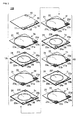
- Figs. 1 and 2 illustrate a piezoelectric element 100 according to a first embodiment of the present invention.
- Fig. 1 is a perspective view
- Fig. 2 is an exploded perspective view.
- the piezoelectric element 100 includes a piezoelectric body 1 having a plurality of laminated piezoelectric layers 1a to 1j.
- piezoelectric ceramics mainly made of PZT may be used to form the piezoelectric body 1.
- a first terminal 11, a second terminal 12, a third terminal 13, a fourth terminal 14, and a fifth terminal 15 are formed in a line. Further, a dummy terminal 16 is formed on a portion distant from these terminals.
- the first terminal 11, the second terminal 12, the third terminal 13, the fourth terminal 14, the fifth terminal 15, and the dummy terminal 16 are connected to the interior of the piezoelectric body 1 via filled vias, which are formed by piercing holes in the piezoelectric layer 1a and filling the holes with a conductive substance.
- connection in each of connecting portions is performed by the use of two filled vias to increase the reliability of connection.
- the connection in each of connecting portions may be performed by the use of a single filled via.
- a relatively large circular ground electrode 21 is formed in a central portion of a surface of the next piezoelectric layer 1b, and a ring-shaped dummy electrode 22 is formed therearound.
- the ground electrode 21 is formed with an extraction electrode 21a along one side of the piezoelectric layer 1b.
- relay electrodes 23a and 23b are formed adjacent to one side of the extraction electrode 21a, and relay electrodes 23c and 23d are formed adjacent to the other side of the extraction electrode 21a.
- the relay electrode 23a, the relay electrode 23b, the extraction electrode 21a, the relay electrode 23c, the relay electrode 23d, and the dummy electrode 22 are connected to the first terminal 11, the second terminal 12, the third terminal 13, the fourth terminal 14, the fifth terminal 15, and the dummy terminal 16, respectively.
- a circular central electrode 24 is formed in a central portion of a surface of the next piezoelectric layer 1c, and a ring-shaped peripheral electrode 25 is formed therearound.
- the central electrode 24 is formed with an extraction electrode 24a along one side of the piezoelectric layer 1c.
- the peripheral electrode 25 is formed with two extraction electrodes 25a and 25b along the same side of the piezoelectric layer 1c, along which the extraction electrode 24a is formed, with the extraction electrode 24a interposed therebetween.
- a ground relay electrode 26 is formed between the extraction electrode 24a and the extraction electrode 25a.
- a relay electrode 23e is formed adjacent to a side of the extraction electrode 25a distant from the ground relay electrode 26.
- the relay electrode 23e, the extraction electrode 25a, the ground relay electrode 26, the extraction electrode 24a, and the extraction electrode 25b are sequentially formed along the one side of the piezoelectric layer 1c.
- a relay electrode 23f is formed in a portion of the surface of the piezoelectric layer 1c diagonal to a portion formed with the relay electrode 23e.
- via filled vias formed in the piezoelectric layer 1b, the relay electrode 23e, the extraction electrode 25a, the ground relay electrode 26, the extraction electrode 24a, the extraction electrode 25b, and the relay electrode 23f are connected to the relay electrode 23a, the relay electrode 23b, the extraction electrode 21a, the relay electrode 23c, the relay electrode 23d, and the dummy electrode 22, respectively.
- the next piezoelectric layer 1d includes the same electrode patterns as those of the above-described piezoelectric layer 1b.
- a surface of the piezoelectric layer 1d is formed with a ground electrode 21, an extraction electrode 21a, a dummy electrode 22, and relay electrodes 23a, 23b, 23c, and 23d.
- the relay electrode 23a, the relay electrode 23b, the extraction electrode 21a, the relay electrode 23c, the relay electrode 23d, and the dummy electrode 22 are connected to the relay electrode 23e, the extraction electrode 25a, the ground relay electrode 26, the extraction electrode 24a, the extraction electrode 25b, and the relay electrode 23f, respectively.
- the next piezoelectric layer 1e includes the same electrode patterns as those of the above-described piezoelectric layer 1c.
- a surface of the piezoelectric layer 1e is formed with a central electrode 24, an extraction electrode 24a, a peripheral electrode 25, extraction electrodes 25a and 25b, a ground relay electrode 26, and relay electrodes 23e and 23f.
- the relay electrode 23e, the extraction electrode 25a, the ground relay electrode 26, the extraction electrode 24a, the extraction electrode 25b, and the relay electrode 23f are connected to the relay electrode 23a, the relay electrode 23b, the extraction electrode 21a, the relay electrode 23c, the relay electrode 23d, and the dummy electrode 22, respectively.
- the next piezoelectric layer 1f includes the same electrode patterns as those of the above-described piezoelectric layers 1b and 1d.
- a surface of the piezoelectric layer 1f is formed with a ground electrode 21, an extraction electrode 21a, a dummy electrode 22, and relay electrodes 23a, 23b, 23c, and 23d.
- the relay electrode 23a, the relay electrode 23b, the extraction electrode 21a, the relay electrode 23c, the relay electrode 23d, and the dummy electrode 22 are connected to the relay electrode 23e, the extraction electrode 25a, the ground relay electrode 26, the extraction electrode 24a, the extraction electrode 25b, and the relay electrode 23f, respectively.
- a surface of the next piezoelectric layer 2g is formed with a central electrode 24, an extraction electrode 24a, a peripheral electrode 25, extraction electrodes 25a and 25b, a ground relay electrode 26, and relay electrodes 23e and 23f, similarly to the above-described piezoelectric layers 1c and 1e, but is different in arrangement (different in order of formation) of some of the electrodes from the piezoelectric layers 1c and 1e. That is, the extraction electrode 25a, the extraction electrode 24a, the ground relay electrode 26, the extraction electrode 25b, and the relay electrode 23e are sequentially formed along one side of the piezoelectric layer 1g.
- via filled vias formed in the piezoelectric layer 1f, the extraction electrode 25a, the extraction electrode 24a, the ground relay electrode 26, the extraction electrode 25b, the relay electrode 23e, and the relay electrode 23f are connected to the relay electrode 23a, the relay electrode 23b, the extraction electrode 21a, the relay electrode 23c, the relay electrode 23d, and the dummy electrode 22, respectively.
- the next piezoelectric layer 1h includes the same electrode patterns as those of the above-described piezoelectric layers 1b, 1d, and 1f.
- a surface of the piezoelectric layer 1n is formed with a ground electrode 21, an extraction electrode 21a, a dummy electrode 22, and relay electrodes 23a, 23b, 23c, and 23d.
- the relay electrode 23a, the relay electrode 23b, the extraction electrode 21a, the relay electrode 23c, the relay electrode 23d, and the dummy electrode 22 are connected to the extraction electrode 25a, the extraction electrode 24a, the ground relay electrode 26, the extraction electrode 25b, the relay electrode 23e, and the relay electrode 23f, respectively.
- the next piezoelectric layer 1i includes the same electrode patterns as those of the above-described piezoelectric layer 1g.
- a surface of the piezoelectric layer 1i is formed with a central electrode 24, an extraction electrode 24a, a peripheral electrode 25, extraction electrodes 25a and 25b, a ground relay electrode 26, and relay electrodes 23e and 23f.
- the extraction electrode 25a, the extraction electrode 24a, the ground relay electrode 26, the extraction electrode 25b, the relay electrode 23e, and the relay electrode 23f are connected to the relay electrode 23a, the relay electrode 23b, the extraction electrode 21a, the relay electrode 23c, the relay electrode 23d, and the dummy electrode 22, respectively.
- the next piezoelectric layer 1j includes the same electrode patterns as those of the above-described piezoelectric layers 1b, 1d, 1f, and 1h.
- a surface of the piezoelectric layer 1j is formed with a ground electrode 21, an extraction electrode 21a, a dummy electrode 22, and relay electrodes 23a, 23b, 23c, and 23d.
- the relay electrode 23a, the relay electrode 23b, the extraction electrode 21a, the relay electrode 23c, the relay electrode 23d, and the dummy electrode 22 are connected to the extraction electrode 25a, the extraction electrode 24a, the ground relay electrode 26, the extraction electrode 25b, the relay electrode 23e, and the relay electrode 23f, respectively.
- the central electrodes 24 formed in a first portion 1A (the piezoelectric layers 1a to 1e) corresponding to the upper half and the peripheral electrodes 25 formed in a second portion 1B (the piezoelectric layers 1f to 1j) corresponding to the lower half are connected to the first terminal 11 and the fourth terminal 14.
- the peripheral electrodes 25 formed in the first portion 1A and the central electrodes 24 formed in the second portion 1B are connected to the second terminal 12 and the fifth terminal 15.
- all of the ground electrodes 21 formed in the piezoelectric body 1 are connected to the third terminal 13.
- all of the dummy terminals 22 formed in the piezoelectric body 1 are connected to the dummy terminal 16.
- the central electrodes 24 formed in the first portion 1A and the peripheral electrodes 25 formed in the second portion 1B may be connected to the second terminal 12 and the fifth terminal 15, and the peripheral electrodes 25 formed in the first portion 1A and the central electrodes 24 formed in the second portion 1B may be connected to the first terminal 11 and the fourth terminal 14.
- the piezoelectric body 1 having the above-described structure is formed by a method of, for example, forming, laminating, compressing, and firing, with a predetermined profile, piezoelectric green sheets for forming the piezoelectric layers 1a to 1j, which are applied with conductive paste on respective surfaces thereof, formed with the necessary terminals (the first terminal 11, the second terminal 12, the third terminal 13, the fourth terminal 14, the fifth terminal 15, and the dummy terminal 16) and the necessary electrodes (the ground electrodes 21, the extraction electrodes 21a, the dummy electrodes 22, the central electrodes 24, the extraction electrodes 24a, the relay electrodes 23a, 23b, 23c, 23d, 23e, and 23f, the peripheral electrodes 25, the extraction electrodes 25a and 25b, and the ground relay electrodes 26), and formed with the necessary filled vias formed by piecing holes and filling the holes with conductive paste.
- the necessary terminals the first terminal 11, the second terminal 12, the third terminal 13, the fourth terminal 14, the fifth terminal 15, and the dummy terminal 16
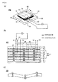
- FIG. 3 are explanatory diagrams illustrating a polarization process of the piezoelectric element 100, and (B) of Fig. 3 illustrates a portion of (A) of Fig. 3 indicated by a dash-dotted line S-S.
- the scale in the height direction is enlarged as compared with that in the width direction to clarify polarization directions.
- the first terminal 11 and the fourth terminal 14 are applied with a positive voltage
- the second terminal 12 and the fifth terminal 15 are applied with a negative voltage
- the third terminal 13 connected to a ground.
- the positive voltage is selected from a range of 30 V to 50 V, for example
- the negative voltage is selected from a range of -50 V to -30 V, for example.
- the time of application ranges from 1 second to 120 seconds, for example.
- the dummy terminal 16 is not used in the polarization process.
- the positive voltage and the negative voltage to be applied may be reversed to apply the negative voltage to the first terminal 11 and the fourth terminal 14 and apply the positive voltage to the second terminal 12 and the fifth terminal 15.
- each of the piezoelectric layers 1b to 1i forming the piezoelectric body 100 is polarized in the directions indicated by arrows in the drawing.
- the piezoelectric layer 1a forming the uppermost layer and the piezoelectric layer 1j forming the lowermost layer are not polarized.
- the polarization direction is opposite between the central portion and the peripheral portion.
- the central electrodes 24 formed in the first portion 1A and the peripheral electrodes 25 formed in the second portion 1B are connected to the first terminal 11 and the fourth terminal 14, and the peripheral electrodes 25 formed in the first portion 1A and the central electrodes 24 formed in the second portion 1B are connected to the second terminal 12 and the fifth terminal 15. Therefore, the repeating order of polarization is different between the piezoelectric layers 1b to 1e of the first portion 1A and the piezoelectric layers 1f to 1i of the second portion 1B.
- the piezoelectric element 100 having such a structure and subjected to polarization is used as, for example, a drive source of a piezoelectric device such as a piezoelectric pump.
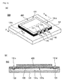
- A) and (B) of Fig. 4 illustrate a piezoelectric pump 200 according to the first embodiment of the present invention using the piezoelectric element 100 as a drive source thereof.
- (A) of Fig. 4 is a perspective view
- (B) of Fig. 4 is a cross-sectional view illustrating a portion of (A) of Fig. 4 indicated by a dash-dotted line T-T.
- the piezoelectric pump 200 includes a pump body 31.
- the pump body 31 is formed with a hollow pump chamber 31a, an opening 31b that opens an upper portion of the pump chamber 31a, and two holes 31c and 31d that communicate with the pump chamber 31a.
- the opening 31b is closed by a diaphragm 32, and the piezoelectric element 100 is bonded and fixed to the diaphragm 32.
- the hole 31c is attached with an inflow check valve 33
- the hole 31d is attached with an outflow check valve 34.
- the inflow check valve 33 functions to allow fluid to flow into the pump chamber 31a from the outside but prevent fluid from flowing out in the opposite direction.
- the outflow check valve 34 functions to allow fluid to flow to the outside from the pump chamber 31a but prevent fluid from flowing in in the opposite direction.
- two metal terminal members 41 and 42 are fixed on the upper surface of the pump body 31. Further, with a bonding material such as conductive paste or solder, the metal terminal member 41 is connected to the first terminal 11 and the second terminal 12 of the piezoelectric element 100, and the metal terminal member 42 is connected to the third terminal 13, respectively. Meanwhile, the fourth terminal 14 and the fifth terminal 15 are not connected to a metal terminal member (the illustration of the boding material is omitted in (A) of Fig. 4 ).
- FIG. 5 illustrates a connection state of the metal terminal member 41, the first terminal 11, and the second terminal 12.
- the metal terminal member 41 is in partial connect with both the first terminal 11 and the second terminal 12.
- the metal terminal member 41 is not in contact with respective portions of the first terminal 11 and the second terminal 12 formed with filled vias (illustrated as black dots in the drawing). This is for preventing breakage or damage of the filled vias and the piezoelectric body 1 due to the contact of the metal terminal member 41 with the filled vias.
- a bonding material such as conductive paste is applied to a portion encircled by a chain line, and thus the first terminal 11, the second terminal 12, and the metal terminal member 41 are connected.
- FIG. 5 illustrate modified examples of the connection of the first terminal 11, the second terminal 12, and the metal terminal member 41.
- the metal terminal member 41 may be configured to be in connect only with one of the terminals, e.g., the second terminal 12, and may be connected to the first terminal 11 as the other terminal by a bonding material.
- the metal terminal member 41 may be configured not to be in connect with either of the two terminals, i.e., the first terminal 11 and the second terminal 12, and may be connected thereto by a bonding material.
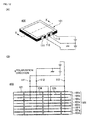
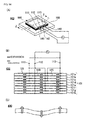
- FIG. 6 illustrates a drive state of the piezoelectric pump 200.
- FIG. 6 are explanatory diagrams, and (B) and (C) of Fig. 6 illustrate a portion of the piezoelectric element 100 in (A) of Fig. 6 indicated by a dash-dotted line U-U.
- the scale in the height direction is enlarged as compared with that in the width direction to clarify the expansion and contraction in the piezoelectric layers 1a to 1j forming the piezoelectric element 100.
- the piezoelectric element 100 has an alternating-current power supply serving as a drive power supply and having one terminal connected to the third terminal 13 via the metal terminal member 42 and the other terminal connected to the first terminal 11 and the second terminal 12 via the metal terminal member 41.
- a power supply that generates an alternating-current voltage of 1 V to 20 V for example, is used.
- the alternating-current power supply is not limited to the one that generates sine waves, and may be the one that generates, for example, rectangular waves.
- the piezoelectric layers 1a to 1j forming the piezoelectric body 1 of the piezoelectric element 100 are polarized, as illustrated in (B) of Fig. 3 (the piezoelectric layer 1a forming the uppermost layer and the piezoelectric layer 1j forming the lowermost layer, however, are not polarized).
- the piezoelectric body 1 When applied with an alternating-current voltage, therefore, the piezoelectric body 1 partially expands or contracts at some point of time, as indicated by arrows in (B) of Fig. 6 , for example. At this point of time, for example, a central portion of the piezoelectric layers 1b to 1e contracts, and a peripheral portion located therearound expands.
- the piezoelectric element 100 has a central portion downwardly bent and displaced and a peripheral portion upwardly bent and displaced, as indicated by hatched arrows in (C) of Fig. 6 .
- the piezoelectric element 100 exhibits an opposite behavior to that illustrated in (B) and (C) of Fig. 6 . That is, the central portion of the piezoelectric layers 1b to 1e expands, and the peripheral portion located therearound contracts. Further, the central portion of the piezoelectric layers 1f to 1i contracts, and the peripheral portion located therearound expands. Then, the piezoelectric element 100 has the central portion upwardly bent and displaced and the peripheral portion downwardly bent and displaced.
- the piezoelectric element 100 repeats these behaviors. Thereby, in the piezoelectric pump 200 illustrated in (A) and (B) of Fig. 4 , fluid is flown into the pump chamber 31a through the hole 31c, and the fluid flown into the pump chamber 31a is flown to the outside through the hole 31d.
- the piezoelectric body 1 is configured to have multiple layers of the piezoelectric layers 1a to 1j, and each of the piezoelectric layers 1b to 1i is polarized in the opposite directions between the central portion and the peripheral portion. It is therefore possible to drive the piezoelectric element 100 with a relatively low voltage, and to obtain a large displacement amount at the central portion of the piezoelectric element 100. Accordingly, the piezoelectric pump 200 according to the present embodiment using the piezoelectric element 100 as a drive source thereof efficiently functions with low power consumption. Further, the central electrode 24 and the peripheral electrode 25 formed on the same layer are constantly applied with the same potential. Therefore, there is no electromigration occurring therebetween, and there is no short circuit occurring therebetween.
- the piezoelectric element 100 is capable of being driven only by the connection of the two metal terminal members 41 and 42, and does not require the connection of three metal terminal members, unlike the existing one. Therefore, the piezoelectric element 100 is easy to mount. Further, the piezoelectric pump 200 using the piezoelectric element 100 as a drive source thereof is improved in degree of design freedom, and is simplified in manufacture.
- the piezoelectric element 100 is configured to have the first portion 1A including five layers of the piezoelectric layers 1a to 1e and the second portion 1B including five layers of the piezoelectric layers 1f to 1j, as illustrated in Fig. 2 and so forth.
- the number of layers is not limited thereto, and may be increased or reduced.
- the piezoelectric layers 1b and 1c may be paired, and a desired number of pairs thereof may be added under the piezoelectric layer 1a, for example.
- the piezoelectric layers 1f and 1g may be paired, and a desired number of pairs thereof may be added under the piezoelectric layer 1e, for example.
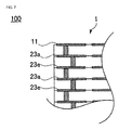
- the filled vias may be formed not to overlap at the same position but to be alternately shifted in position, as illustrated in Fig. 7 , when viewed through in the lamination direction. In this case, it is possible to prevent the deformation of the piezoelectric body 1 due to serial formation of the filled vias in the lamination direction.
- a rectangular relay electrode 23g, a circular relay electrode 23h, a rectangular relay electrode 23i, and a circular relay electrode 23j may be laminated, as illustrated in (A) of Fig. 8 .
- relay electrodes 23k to 23n of a given shape, such as a rectangular shape, for example, each rotated by a predetermined angle may be laminated.
- relay electrodes 23o to 23r of a given shape such as a rectangular shape, for example, each shifted in position in the horizontal direction may be laminated.
- a given shape such as a rectangular shape, for example, each shifted in position in the horizontal direction
- the alternating-current power supply serving as a drive source has one terminal connected to the third terminal 13 and the other terminal connected to the first terminal 11 and the second terminal 12.
- the other terminal of the alternating-current power supply may be connected to the fourth terminal 14 and the fifth terminal 15 in place of the first terminal 11 and the second terminal 12.
- the piezoelectric device using the piezoelectric element 100 as a drive source thereof is not limited to the piezoelectric pump, and may be a piezoelectric blower or a piezoelectric fan, for example.
- Fig. 9 illustrates a piezoelectric element 300 according to a second embodiment of the present invention.
- Fig. 9 is a perspective view.
- electrical connection between layers inside the piezoelectric body 1 is performed via the filled vias formed in the piezoelectric layers 1a to 1i (see Figs. 1 and 2 ).
- each of the ground connection electrodes, the relay electrodes, and the extraction electrodes formed on the piezoelectric layers is formed to be in contact with a side of the corresponding piezoelectric layer, although not illustrated.
- the other configurations of the piezoelectric element 300 according to the second embodiment are the same as those of the piezoelectric element 100 according to the first embodiment.
- electrical connection between layers may be performed via terminals each formed on a side surface of the piezoelectric body 1, in place of the filled vias.
Landscapes
- Engineering & Computer Science (AREA)
- Mechanical Engineering (AREA)
- General Engineering & Computer Science (AREA)
- Reciprocating Pumps (AREA)
- General Electrical Machinery Utilizing Piezoelectricity, Electrostriction Or Magnetostriction (AREA)
Applications Claiming Priority (2)
| Application Number | Priority Date | Filing Date | Title |
|---|---|---|---|
| JP2011043847 | 2011-03-01 | ||
| PCT/JP2012/053147 WO2012117831A1 (ja) | 2011-03-01 | 2012-02-10 | 圧電素子およびこれを用いた圧電装置 |
Publications (2)
| Publication Number | Publication Date |
|---|---|
| EP2682995A1 true EP2682995A1 (de) | 2014-01-08 |
| EP2682995A4 EP2682995A4 (de) | 2014-10-22 |
Family
ID=46757770
Family Applications (1)
| Application Number | Title | Priority Date | Filing Date |
|---|---|---|---|
| EP12752085.6A Withdrawn EP2682995A4 (de) | 2011-03-01 | 2012-02-10 | Piezoelektrisches element und piezoelektrische vorrichtung damit |
Country Status (5)
| Country | Link |
|---|---|
| US (1) | US9406861B2 (de) |
| EP (1) | EP2682995A4 (de) |
| JP (1) | JP5500308B2 (de) |
| CN (1) | CN103392244B (de) |
| WO (1) | WO2012117831A1 (de) |
Families Citing this family (9)
| Publication number | Priority date | Publication date | Assignee | Title |
|---|---|---|---|---|
| JP6106404B2 (ja) * | 2012-10-30 | 2017-03-29 | 太陽誘電株式会社 | 電子部品モジュール |
| DE102012111972A1 (de) * | 2012-12-07 | 2014-06-12 | Epcos Ag | Verfahren zur Herstellung eines elektronischen Bauteils |
| US9813823B2 (en) | 2014-01-30 | 2017-11-07 | Kyocera Corporation | Piezoelectric element, and piezoelectric vibrating apparatus, portable terminal, sound generator, sound generating apparatus, and electronic device comprising the piezoelectric element |
| JP6361640B2 (ja) * | 2015-11-30 | 2018-07-25 | Tdk株式会社 | 圧電素子及び圧電アクチュエータ |
| US10618551B2 (en) * | 2016-02-01 | 2020-04-14 | Ford Global Technologies, Llc | Clearance and preload adjustment for steering mechanism using piezoelectric elements |
| JP6648821B2 (ja) * | 2016-04-15 | 2020-02-14 | 第一精工株式会社 | スピーカシステム |
| JP6729015B2 (ja) * | 2016-06-08 | 2020-07-22 | Tdk株式会社 | 圧電素子 |
| JP6680415B2 (ja) * | 2017-12-22 | 2020-04-15 | 株式会社村田製作所 | ポンプ |
| JP2024034326A (ja) * | 2022-08-31 | 2024-03-13 | Tdk株式会社 | 圧電素子 |
Family Cites Families (21)
| Publication number | Priority date | Publication date | Assignee | Title |
|---|---|---|---|---|
| US4257686A (en) * | 1978-12-14 | 1981-03-24 | Itek Corporation | Multiple layer piezoelectric wavefront modulator |
| JPH03171784A (ja) * | 1989-11-30 | 1991-07-25 | Toshiba Corp | バイモルフ素子 |
| JP3402256B2 (ja) * | 1999-05-25 | 2003-05-06 | 株式会社村田製作所 | 積層型圧電部品 |
| WO2000074153A1 (en) * | 1999-05-31 | 2000-12-07 | Nanomotion Ltd. | Multilayer piezoelectric motor |
| US6933657B2 (en) * | 2001-03-30 | 2005-08-23 | Canon Kabushiki Kaisha | Stacked electro-mechanical energy conversion element and method of manufacturing the same |
| JP4511120B2 (ja) * | 2002-04-03 | 2010-07-28 | オリンパス株式会社 | 超音波リニアモータ |
| WO2005067070A1 (de) * | 2004-01-12 | 2005-07-21 | Siemens Aktiengesellschaft | Aktor mit innenliegender anschlusselektrode und herstellungsverfahren für einen solchen aktor |
| TWI270332B (en) * | 2004-04-20 | 2007-01-01 | Murata Manufacturing Co | Multilayer ceramic board, manufacturing method thereof and piezoelectric resonant component |
| JP2006004980A (ja) * | 2004-06-15 | 2006-01-05 | Canon Inc | 積層電気−機械エネルギー変換素子及び振動波駆動装置 |
| JP4576185B2 (ja) * | 2004-09-22 | 2010-11-04 | オリンパス株式会社 | 超音波振動子 |
| JP2006157172A (ja) * | 2004-11-25 | 2006-06-15 | Murata Mfg Co Ltd | 圧電フィルタ装置 |
| KR100691280B1 (ko) * | 2005-09-05 | 2007-03-12 | 삼성전기주식회사 | 압전 진동자, 그 제조방법 및 압전 진동자를 구비하는 선형액추에이터 |
| JP4069160B2 (ja) * | 2006-01-23 | 2008-04-02 | 松下電器産業株式会社 | 超音波アクチュエータ |
| EP2039934B1 (de) * | 2006-07-11 | 2018-10-17 | Murata Manufacturing Co. Ltd. | Piezoelektrische pumpe |
| CN101622451B (zh) * | 2007-12-03 | 2011-05-11 | 株式会社村田制作所 | 压电泵 |
| JP5234008B2 (ja) * | 2008-04-17 | 2013-07-10 | 株式会社村田製作所 | 積層型圧電素子及び圧電ポンプ |
| US7932661B2 (en) * | 2008-09-23 | 2011-04-26 | Nikko Company | Piezoelectric vibrator for ultrasonic motor |
| AU2009335654A1 (en) * | 2008-12-18 | 2011-06-30 | Discovery Technology International, Inc. | Piezoelectric quasi-resonance motors based on acoustic standing waves with combined resonator |
| JP5429140B2 (ja) * | 2010-01-19 | 2014-02-26 | Tdk株式会社 | 圧電アクチュエータ |
| KR20130104338A (ko) * | 2012-03-13 | 2013-09-25 | 삼성전기주식회사 | 적층 세라믹 전자부품 및 그 제조방법 |
| US9579691B2 (en) * | 2013-05-21 | 2017-02-28 | Mplus Co., Ltd. | Piezoelectric element and electronic component including the same |
-
2012
- 2012-02-10 WO PCT/JP2012/053147 patent/WO2012117831A1/ja not_active Ceased
- 2012-02-10 JP JP2013502228A patent/JP5500308B2/ja active Active
- 2012-02-10 CN CN201280010524.8A patent/CN103392244B/zh active Active
- 2012-02-10 EP EP12752085.6A patent/EP2682995A4/de not_active Withdrawn
-
2013
- 2013-08-19 US US13/969,759 patent/US9406861B2/en active Active
Non-Patent Citations (2)
| Title |
|---|
| No further relevant documents disclosed * |
| See also references of WO2012117831A1 * |
Also Published As
| Publication number | Publication date |
|---|---|
| US20130334933A1 (en) | 2013-12-19 |
| EP2682995A4 (de) | 2014-10-22 |
| CN103392244A (zh) | 2013-11-13 |
| CN103392244B (zh) | 2016-01-20 |
| WO2012117831A1 (ja) | 2012-09-07 |
| US9406861B2 (en) | 2016-08-02 |
| JPWO2012117831A1 (ja) | 2014-07-07 |
| JP5500308B2 (ja) | 2014-05-21 |
Similar Documents
| Publication | Publication Date | Title |
|---|---|---|
| US9406861B2 (en) | Piezoelectric element and piezoelectric device using the same | |
| US20100239444A1 (en) | Layered piezoelectric element and piezoelectric pump | |
| US11189777B2 (en) | Multilayer piezoelectric element and vibrating device | |
| US20100007244A1 (en) | Piezoelectric Motor and Method of Manufacturing the Same | |
| JPH08242025A (ja) | 圧電アクチュエータ | |
| JP2008175097A (ja) | 圧電ポンプ | |
| JP2016051895A (ja) | 圧電素子及びこれを含む圧電振動モジュール | |
| US8441175B2 (en) | Piezoactuator having electrical contact | |
| JP2008211054A (ja) | 積層型圧電素子 | |
| JP2016175274A5 (de) | ||
| WO2013115341A1 (ja) | 積層型圧電素子およびこれを備えた噴射装置ならびに燃料噴射システム | |
| JP5974493B2 (ja) | 圧電ポンプ、圧電ポンプの製造方法 | |
| JP5377100B2 (ja) | 積層型圧電素子、これを用いた噴射装置および燃料噴射システム | |
| US7282839B2 (en) | Multilayer piezoelectric device | |
| KR101170892B1 (ko) | 압전 액추에이터 | |
| US7352115B2 (en) | Piezoelectric element and piezoelectric device | |
| US20170290165A1 (en) | Thin film component sheet, board with built-in electronic component, and method of manufacturing the thin film component sheet | |
| US7170217B2 (en) | Stack-type piezoelectric device | |
| US20130248623A1 (en) | Piezoelectric Component with Contact | |
| JP2005045086A (ja) | インジェクタ装置用積層型圧電素子 | |
| KR20110075193A (ko) | 압전 적층 세라믹 소자 및 그 제조 방법 | |
| JP2017188628A (ja) | 圧電素子、その製造方法および圧電アクチュエータ | |
| JP5087822B2 (ja) | 圧電素子 | |
| JP2012209427A (ja) | 圧電アクチュエータ | |
| KR20160007029A (ko) | 압전 소자 및 이를 포함하는 압전 진동 모듈 |
Legal Events
| Date | Code | Title | Description |
|---|---|---|---|
| PUAI | Public reference made under article 153(3) epc to a published international application that has entered the european phase |
Free format text: ORIGINAL CODE: 0009012 |
|
| 17P | Request for examination filed |
Effective date: 20130830 |
|
| AK | Designated contracting states |
Kind code of ref document: A1 Designated state(s): AL AT BE BG CH CY CZ DE DK EE ES FI FR GB GR HR HU IE IS IT LI LT LU LV MC MK MT NL NO PL PT RO RS SE SI SK SM TR |
|
| DAX | Request for extension of the european patent (deleted) | ||
| A4 | Supplementary search report drawn up and despatched |
Effective date: 20140919 |
|
| RIC1 | Information provided on ipc code assigned before grant |
Ipc: F04B 43/04 20060101ALI20140915BHEP Ipc: H01L 41/083 20060101ALI20140915BHEP Ipc: H01L 41/047 20060101AFI20140915BHEP |
|
| STAA | Information on the status of an ep patent application or granted ep patent |
Free format text: STATUS: THE APPLICATION HAS BEEN WITHDRAWN |
|
| 18W | Application withdrawn |
Effective date: 20150420 |