WO2012117973A1 - 有機エレクトロルミネッセンス素子 - Google Patents
有機エレクトロルミネッセンス素子 Download PDFInfo
- Publication number
- WO2012117973A1 WO2012117973A1 PCT/JP2012/054605 JP2012054605W WO2012117973A1 WO 2012117973 A1 WO2012117973 A1 WO 2012117973A1 JP 2012054605 W JP2012054605 W JP 2012054605W WO 2012117973 A1 WO2012117973 A1 WO 2012117973A1
- Authority
- WO
- WIPO (PCT)
- Prior art keywords
- group
- organic
- transport layer
- bonded
- arylamine compound
- Prior art date
- Legal status (The legal status is an assumption and is not a legal conclusion. Google has not performed a legal analysis and makes no representation as to the accuracy of the status listed.)
- Ceased
Links
- 0 Oc(c(*(c(cc1)ccc1-c1ccccc1)c(cc1)ccc1-c1ccc(*(c(cc2)ccc2-c2ccccc2)c(c(O)c(c(O)c2O)O)c2O)cc1)c(c(O)c1O)O)c1O Chemical compound Oc(c(*(c(cc1)ccc1-c1ccccc1)c(cc1)ccc1-c1ccc(*(c(cc2)ccc2-c2ccccc2)c(c(O)c(c(O)c2O)O)c2O)cc1)c(c(O)c1O)O)c1O 0.000 description 3
Images
Classifications
-
- H—ELECTRICITY
- H10—SEMICONDUCTOR DEVICES; ELECTRIC SOLID-STATE DEVICES NOT OTHERWISE PROVIDED FOR
- H10K—ORGANIC ELECTRIC SOLID-STATE DEVICES
- H10K85/00—Organic materials used in the body or electrodes of devices covered by this subclass
- H10K85/60—Organic compounds having low molecular weight
- H10K85/631—Amine compounds having at least two aryl rest on at least one amine-nitrogen atom, e.g. triphenylamine
-
- C—CHEMISTRY; METALLURGY
- C07—ORGANIC CHEMISTRY
- C07C—ACYCLIC OR CARBOCYCLIC COMPOUNDS
- C07C211/00—Compounds containing amino groups bound to a carbon skeleton
- C07C211/43—Compounds containing amino groups bound to a carbon skeleton having amino groups bound to carbon atoms of six-membered aromatic rings of the carbon skeleton
- C07C211/54—Compounds containing amino groups bound to a carbon skeleton having amino groups bound to carbon atoms of six-membered aromatic rings of the carbon skeleton having amino groups bound to two or three six-membered aromatic rings
-
- C—CHEMISTRY; METALLURGY
- C07—ORGANIC CHEMISTRY
- C07C—ACYCLIC OR CARBOCYCLIC COMPOUNDS
- C07C211/00—Compounds containing amino groups bound to a carbon skeleton
- C07C211/43—Compounds containing amino groups bound to a carbon skeleton having amino groups bound to carbon atoms of six-membered aromatic rings of the carbon skeleton
- C07C211/54—Compounds containing amino groups bound to a carbon skeleton having amino groups bound to carbon atoms of six-membered aromatic rings of the carbon skeleton having amino groups bound to two or three six-membered aromatic rings
- C07C211/56—Compounds containing amino groups bound to a carbon skeleton having amino groups bound to carbon atoms of six-membered aromatic rings of the carbon skeleton having amino groups bound to two or three six-membered aromatic rings the carbon skeleton being further substituted by halogen atoms or by nitro or nitroso groups
-
- C—CHEMISTRY; METALLURGY
- C07—ORGANIC CHEMISTRY
- C07C—ACYCLIC OR CARBOCYCLIC COMPOUNDS
- C07C211/00—Compounds containing amino groups bound to a carbon skeleton
- C07C211/43—Compounds containing amino groups bound to a carbon skeleton having amino groups bound to carbon atoms of six-membered aromatic rings of the carbon skeleton
- C07C211/57—Compounds containing amino groups bound to a carbon skeleton having amino groups bound to carbon atoms of six-membered aromatic rings of the carbon skeleton having amino groups bound to carbon atoms of six-membered aromatic rings being part of condensed ring systems of the carbon skeleton
- C07C211/58—Naphthylamines; N-substituted derivatives thereof
-
- C—CHEMISTRY; METALLURGY
- C09—DYES; PAINTS; POLISHES; NATURAL RESINS; ADHESIVES; COMPOSITIONS NOT OTHERWISE PROVIDED FOR; APPLICATIONS OF MATERIALS NOT OTHERWISE PROVIDED FOR
- C09K—MATERIALS FOR MISCELLANEOUS APPLICATIONS, NOT PROVIDED FOR ELSEWHERE
- C09K11/00—Luminescent materials, e.g. electroluminescent or chemiluminescent
- C09K11/06—Luminescent materials, e.g. electroluminescent or chemiluminescent containing organic luminescent materials
-
- H—ELECTRICITY
- H05—ELECTRIC TECHNIQUES NOT OTHERWISE PROVIDED FOR
- H05B—ELECTRIC HEATING; ELECTRIC LIGHT SOURCES NOT OTHERWISE PROVIDED FOR; CIRCUIT ARRANGEMENTS FOR ELECTRIC LIGHT SOURCES, IN GENERAL
- H05B33/00—Electroluminescent light sources
- H05B33/10—Apparatus or processes specially adapted to the manufacture of electroluminescent light sources
-
- H—ELECTRICITY
- H05—ELECTRIC TECHNIQUES NOT OTHERWISE PROVIDED FOR
- H05B—ELECTRIC HEATING; ELECTRIC LIGHT SOURCES NOT OTHERWISE PROVIDED FOR; CIRCUIT ARRANGEMENTS FOR ELECTRIC LIGHT SOURCES, IN GENERAL
- H05B33/00—Electroluminescent light sources
- H05B33/12—Light sources with substantially two-dimensional [2D] radiating surfaces
- H05B33/14—Light sources with substantially two-dimensional [2D] radiating surfaces characterised by the chemical or physical composition or the arrangement of the electroluminescent material, or by the simultaneous addition of the electroluminescent material in or onto the light source
-
- H—ELECTRICITY
- H10—SEMICONDUCTOR DEVICES; ELECTRIC SOLID-STATE DEVICES NOT OTHERWISE PROVIDED FOR
- H10K—ORGANIC ELECTRIC SOLID-STATE DEVICES
- H10K85/00—Organic materials used in the body or electrodes of devices covered by this subclass
- H10K85/60—Organic compounds having low molecular weight
- H10K85/649—Aromatic compounds comprising a hetero atom
- H10K85/657—Polycyclic condensed heteroaromatic hydrocarbons
- H10K85/6572—Polycyclic condensed heteroaromatic hydrocarbons comprising only nitrogen in the heteroaromatic polycondensed ring system, e.g. phenanthroline or carbazole
-
- C—CHEMISTRY; METALLURGY
- C07—ORGANIC CHEMISTRY
- C07C—ACYCLIC OR CARBOCYCLIC COMPOUNDS
- C07C2601/00—Systems containing only non-condensed rings
- C07C2601/12—Systems containing only non-condensed rings with a six-membered ring
- C07C2601/14—The ring being saturated
-
- C—CHEMISTRY; METALLURGY
- C07—ORGANIC CHEMISTRY
- C07C—ACYCLIC OR CARBOCYCLIC COMPOUNDS
- C07C2603/00—Systems containing at least three condensed rings
- C07C2603/02—Ortho- or ortho- and peri-condensed systems
- C07C2603/04—Ortho- or ortho- and peri-condensed systems containing three rings
- C07C2603/06—Ortho- or ortho- and peri-condensed systems containing three rings containing at least one ring with less than six ring members
- C07C2603/10—Ortho- or ortho- and peri-condensed systems containing three rings containing at least one ring with less than six ring members containing five-membered rings
- C07C2603/12—Ortho- or ortho- and peri-condensed systems containing three rings containing at least one ring with less than six ring members containing five-membered rings only one five-membered ring
- C07C2603/18—Fluorenes; Hydrogenated fluorenes
-
- C—CHEMISTRY; METALLURGY
- C09—DYES; PAINTS; POLISHES; NATURAL RESINS; ADHESIVES; COMPOSITIONS NOT OTHERWISE PROVIDED FOR; APPLICATIONS OF MATERIALS NOT OTHERWISE PROVIDED FOR
- C09K—MATERIALS FOR MISCELLANEOUS APPLICATIONS, NOT PROVIDED FOR ELSEWHERE
- C09K2211/00—Chemical nature of organic luminescent or tenebrescent compounds
- C09K2211/10—Non-macromolecular compounds
- C09K2211/1003—Carbocyclic compounds
- C09K2211/1007—Non-condensed systems
-
- C—CHEMISTRY; METALLURGY
- C09—DYES; PAINTS; POLISHES; NATURAL RESINS; ADHESIVES; COMPOSITIONS NOT OTHERWISE PROVIDED FOR; APPLICATIONS OF MATERIALS NOT OTHERWISE PROVIDED FOR
- C09K—MATERIALS FOR MISCELLANEOUS APPLICATIONS, NOT PROVIDED FOR ELSEWHERE
- C09K2211/00—Chemical nature of organic luminescent or tenebrescent compounds
- C09K2211/10—Non-macromolecular compounds
- C09K2211/1003—Carbocyclic compounds
- C09K2211/1011—Condensed systems
-
- C—CHEMISTRY; METALLURGY
- C09—DYES; PAINTS; POLISHES; NATURAL RESINS; ADHESIVES; COMPOSITIONS NOT OTHERWISE PROVIDED FOR; APPLICATIONS OF MATERIALS NOT OTHERWISE PROVIDED FOR
- C09K—MATERIALS FOR MISCELLANEOUS APPLICATIONS, NOT PROVIDED FOR ELSEWHERE
- C09K2211/00—Chemical nature of organic luminescent or tenebrescent compounds
- C09K2211/10—Non-macromolecular compounds
- C09K2211/1003—Carbocyclic compounds
- C09K2211/1014—Carbocyclic compounds bridged by heteroatoms, e.g. N, P, Si or B
-
- C—CHEMISTRY; METALLURGY
- C09—DYES; PAINTS; POLISHES; NATURAL RESINS; ADHESIVES; COMPOSITIONS NOT OTHERWISE PROVIDED FOR; APPLICATIONS OF MATERIALS NOT OTHERWISE PROVIDED FOR
- C09K—MATERIALS FOR MISCELLANEOUS APPLICATIONS, NOT PROVIDED FOR ELSEWHERE
- C09K2211/00—Chemical nature of organic luminescent or tenebrescent compounds
- C09K2211/10—Non-macromolecular compounds
- C09K2211/1018—Heterocyclic compounds
- C09K2211/1025—Heterocyclic compounds characterised by ligands
- C09K2211/1029—Heterocyclic compounds characterised by ligands containing one nitrogen atom as the heteroatom
-
- H—ELECTRICITY
- H10—SEMICONDUCTOR DEVICES; ELECTRIC SOLID-STATE DEVICES NOT OTHERWISE PROVIDED FOR
- H10K—ORGANIC ELECTRIC SOLID-STATE DEVICES
- H10K2102/00—Constructional details relating to the organic devices covered by this subclass
- H10K2102/10—Transparent electrodes, e.g. using graphene
- H10K2102/101—Transparent electrodes, e.g. using graphene comprising transparent conductive oxides [TCO]
- H10K2102/103—Transparent electrodes, e.g. using graphene comprising transparent conductive oxides [TCO] comprising indium oxides, e.g. ITO
Definitions
- the present invention relates to an organic electroluminescence device which is a self-luminous device suitable for various display devices. Specifically, the present invention relates to an organic electroluminescence device using a specific arylamine derivative (hereinafter referred to as “electroluminescent device”). It may be abbreviated as an organic EL element).
- organic electroluminescence device using a specific arylamine derivative (hereinafter referred to as “electroluminescent device”). It may be abbreviated as an organic EL element).
- the organic EL element is a self-luminous element, it has been actively researched because it is brighter and more visible than a liquid crystal element and has a clear display.
- the light injected from both electrodes is recombined in the light emitting layer to obtain light emission.
- the driving voltage reduces the driving voltage
- phthalocyanines such as copper phthalocyanine (CuPc) were proposed at the beginning (see, for example, Patent Document 3).
- a material having a diamine structure has been widely used (see Patent Document 4).
- arylamine-based materials containing a benzidine skeleton have been used as hole transport materials (see Patent Document 5).
- the hole mobility of a generally used hole transport material is In contrast, the electron mobility of Alq 3 is low, and the work function of Alq 3 is 5.8 eV, which is not a sufficient hole blocking capability. There is a problem in that a part of the hole passes through the light emitting layer and efficiency is lowered.
- the ionization potential value and electron affinity value of the material are set in stages, and the hole injection layer and the electron injection layer respectively.
- Patent Document 6 a device in which two or more layers are stacked has been developed (see Patent Document 6), it cannot be said that the materials used are sufficient in any of light emission efficiency, drive voltage, and device life.
- the hole transport layer is usually an extremely thin film, it is affected by the roughness of the surface of a transparent electrode such as an ITO electrode used as an anode, and thus, due to occurrence of a short circuit of the fabricated device. The probability of defective products was high.
- the film thickness of the hole transport layer is increased, the roughness of the surface of the anode such as the ITO electrode can be covered, and the probability of occurrence of defective products of the manufactured element can be lowered.
- the driving voltage becomes high and exceeds the practical driving voltage. That is, light emission at a practical driving voltage becomes difficult.
- JP-A-8-48656 Japanese Patent No. 3194657 U.S. Pat. No. 4,720,432 JP-A-8-291115 Japanese Patent No. 3529735 JP-A-6-314594 Japanese Patent Laid-Open No. 7-126615 Japanese Patent No. 8-048656 JP 2005-108804 A
- the object of the present invention is to combine various materials for organic EL elements having excellent hole and electron injection / transport performance, thin film stability and durability, so that the characteristics of each material can be effectively expressed.
- an object of the present invention is to provide an organic EL element with high efficiency, low driving voltage, and long life.
- the present inventors pay attention to the fact that the arylamine-based material is excellent in hole injection and transport capability, and stability and durability of the thin film.
- a variety of organic EL devices were selected by combining these compounds so that holes can be efficiently injected and transported to the light-emitting layer, and the characteristics of the devices were intensively evaluated. As a result, the present invention has been completed.
- an organic electroluminescence device in which a hole transport layer, a light emitting layer and an electron transport layer are provided between an anode and a cathode,
- the hole transport layer comprises an arylamine compound (X) having a molecular structure in which three or more triphenylamine skeletons are bonded by a single bond or a divalent hydrocarbon group, and two triphenylamine skeletons.
- an organic electroluminescence device comprising an arylamine compound (Y) having a molecular structure bonded with a single bond or a divalent hydrocarbon group.
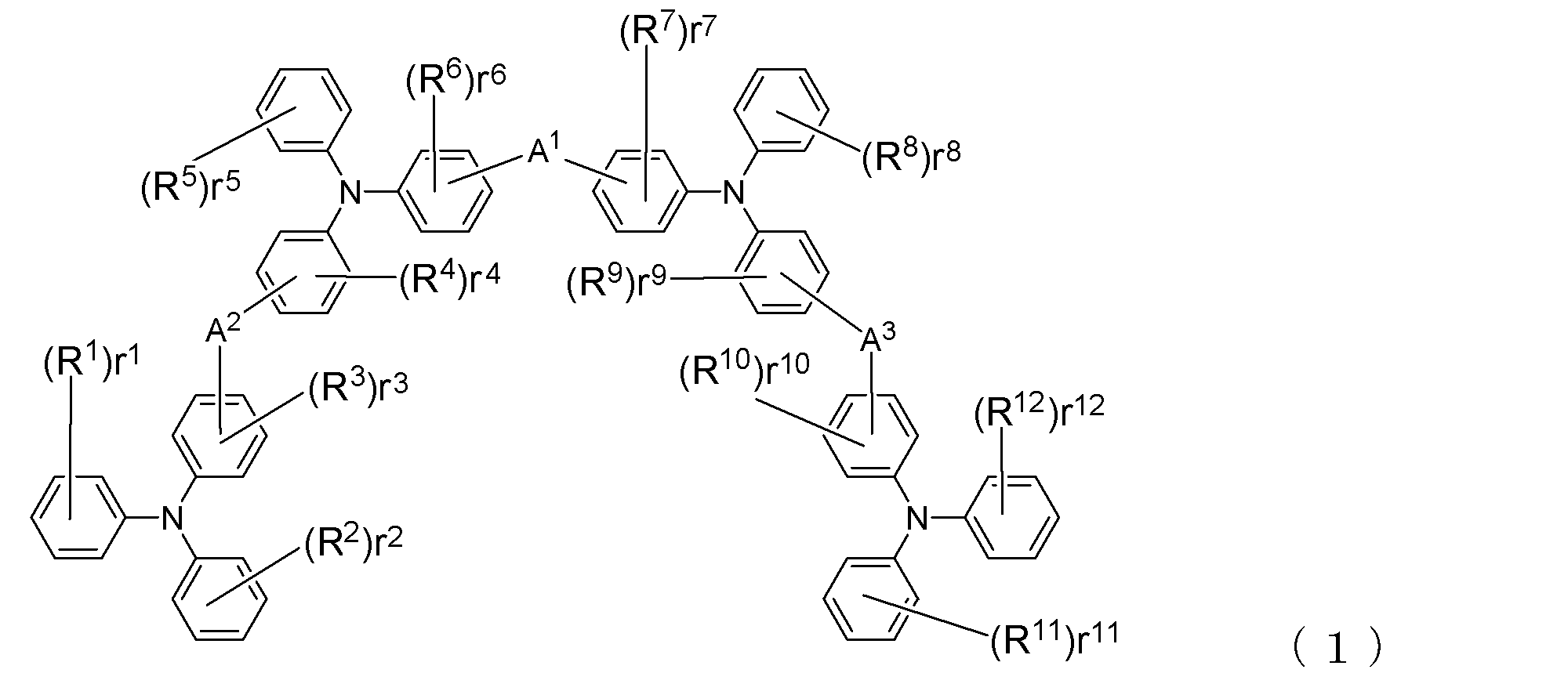
- the arylamine compound (X) is preferably represented by the following general formula (1).
- r 1 to r 12 represent the numbers of R 1 to R 12 , respectively.
- r 1 , r 2 , r 5 , r 8 , r 11 and r 12 represent an integer of 0 to 5;
- r 3 , r 4 , r 6 , r 7 , r 9 and r 10 represent an integer of 0 to 4;
- R 1 to R 12 are each a deuterium atom, a fluorine atom, a chlorine atom, A cyano group, a trifluoromethyl group, an unsubstituted alkyl group having 1 to 6 carbon atoms, an unsubstituted or substituted alkenyl group having 2 to 6 carbon atoms, an unsubstituted or substituted aromatic hydrocarbon group, or an unsubstituted or substituted aromatic group Group bicyclic groups, and these groups bonded to the
- At least one of R 1 to R 12 is preferably a deuterium atom or a group containing a deuterium atom.
- the arylamine compound (Y) is preferably represented by the following general formula (2).
- r 13 to r 18 indicate the number of R 13 to R 18
- r 13 , r 14 , r 17 and r 18 are integers from 0 to 5
- r 15 and r 16 Represents an integer from 0 to 4
- R 13 to R 18 are each a deuterium atom, a fluorine atom, a chlorine atom, A cyano group, a trifluoromethyl group, an unsubstituted alkyl group having 1 to 6 carbon atoms, an unsubstituted or substituted alkenyl group having 2 to 6 carbon atoms, an unsubstituted or substituted aromatic hydrocarbon group, or an unsubstituted or substituted aromatic group Group bicyclic groups, and these groups bonded to the same benzene ring may be bonded to each other to form a ring
- a 4 represents a single bond or a divalent hydrocarbon group represented by
- At least one of R 13 to R 18 is preferably a deuterium atom or a group containing a deuterium atom.
- the organic EL device of the present invention hole transport is performed by an arylamine compound (X) having three or more triphenylamine skeletons in the molecule and an arylamine compound (Y) having two triphenylamine skeletons in the molecule. It is a remarkable feature that a layer is formed. That is, the hole transport layer containing a combination of such arylamine compounds (X) and (Y) has a high hole movement speed, a stable thin film state, and excellent heat resistance. . Therefore, the organic EL device of the present invention can efficiently inject and transport holes from the hole transport layer to the light emitting layer, exhibit high light emission efficiency, and have a low driving voltage. As a result, a long life can be realized.
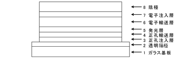
- FIG. 3 is a diagram showing the configurations of organic EL elements of Examples 1 to 6 and Comparative Examples 1 to 5.
- the organic EL device of the present invention has a basic structure in which a hole transport layer, a light emitting layer, and an electron transport layer are formed in this order between an anode and a cathode.
- the transport layer has a structure formed of two kinds of arylamine compounds (X) and (Y) having a triphenylamine skeleton.
- X arylamine compounds
- Y triphenylamine skeleton
- the anode is provided by vapor deposition on a transparent substrate such as a transparent plastic substrate (for example, a polyethylene terephthalate substrate) or a glass substrate, and is formed of an electrode material having a large work function such as ITO or gold.
- a transparent substrate such as a transparent plastic substrate (for example, a polyethylene terephthalate substrate) or a glass substrate, and is formed of an electrode material having a large work function such as ITO or gold.
- the hole transport layer located on the anode side with respect to the light emitting layer contains two types of arylamine compounds (X) and (Y) having a triphenylamine skeleton.
- Arylamine compound (X) One arylamine compound (X) has three or more triphenylamine skeletons, and these triphenylamine skeletons are single bonds or divalent hydrocarbon groups (that is, those containing no heteroatoms). Valent group). This arylamine compound (X) has a higher hole mobility than the arylamine compound (Y) described later.
- Such an arylamine compound (X) is, for example, various triphenylamine trimers or tetramers, and has four triphenylamine skeletons particularly in terms of high hole mobility. Is preferred.
- Examples of the arylamine having four triphenylamine skeletons include those represented by the following general formula (1).
- r 1 to r 12 represent the number of groups R 1 to R 12 that can be bonded to each benzene ring in the molecule
- r 1 , r 2 , r 5 , r 8 , r 11 and r 12 represent an integer of 0 to 5
- r 3 , r 4 , r 6 , r 7 , r 9 and r 10 represent an integer of 0 to 4. That is, the value of r 1 to r 12 being 0 means that the groups R 1 to R 12 are not bonded to the benzene ring.
- R 1 to R 12 may be the same or different and each includes a deuterium atom, a fluorine atom, a chlorine atom, a cyano group, a trifluoromethyl group, an unsubstituted alkyl group having 1 to 6 carbon atoms, or 1 to 6 carbon atoms.
- a plurality of groups R 1 to R 12 (when r 1 to r 12 is 2 or more) may be bonded to each other to form a ring.
- the unsubstituted alkyl group having 1 to 6 carbon atoms may be linear or branched, and examples thereof include a methyl group, an ethyl group, an n-propyl group, an isopropyl group, Examples thereof include n-butyl group, isobutyl group, tert-butyl group, n-pentyl group, isopentyl group, neopentyl group, n-hexyl group and the like.
- the unsubstituted alkenyl group having 2 to 6 carbon atoms may be linear or branched, and examples thereof include a vinyl group, an allyl group, an isopropenyl group, and a 2-butenyl group.
- aromatic hydrocarbon group examples include phenyl group, biphenylyl group, terphenylyl group, tetrakisphenyl group, styryl group, naphthyl group, anthryl group, acenaphthenyl group, fluorenyl group, phenanthryl group and the like.
- Aromatic heterocyclic groups include indenyl, pyrenyl, pyridyl, pyrimidyl, furanyl, pyronyl, thienyl, quinolyl, isoquinolyl, benzofuranyl, benzothienyl, indolyl, carbazolyl, benzox Examples include zolyl group, benzothiazolyl group, quinoxalyl group, benzimidazolyl group, pyrazolyl group, dibenzofuranyl group, dibenzothienyl group, naphthyridinyl group, phenanthrolinyl group, acridinyl group and the like.
- any of the above alkenyl groups, aromatic hydrocarbon groups and aromatic heterocyclic groups may have a substituent.
- substituents include deuterium atom, fluorine atom, chlorine atom, trifluoromethyl group, alkyl group having 1 to 6 carbon atoms, phenyl group, biphenylyl group, terphenylyl group, tetrakisphenyl group, styryl group, naphthyl group.
- a fluorenyl group, a phenanthryl group, an indenyl group, and a pyrenyl group, and these substituents may further have a substituent.
- a plurality of groups R 1 to R 12 when bonded to each other to form a ring, they may be bonded to each other via a single bond to form a ring, or have a substituent. And may be bonded to each other via a methylene group, an oxygen atom or a sulfur atom which may be formed to form a ring. In particular, it is preferable that they are bonded to each other via a dimethylmethylene group to form a ring.
- At least one of R 1 to R 12 is a deuterium atom or a group containing a deuterium atom, for example, an alkenyl group, an aromatic hydrocarbon group or an aromatic group having a deuterium atom as a substituent. It is preferably a heterocyclic group.
- a 1 to A 3 correspond to the bonding portion between the triphenylamine skeletons and represent a single bond or a divalent hydrocarbon group.
- Examples of the divalent hydrocarbon group that is, a divalent group containing no hetero atom, include those represented by the following structural formulas (B) to (F).
- n1 is an integer of 1 to 3
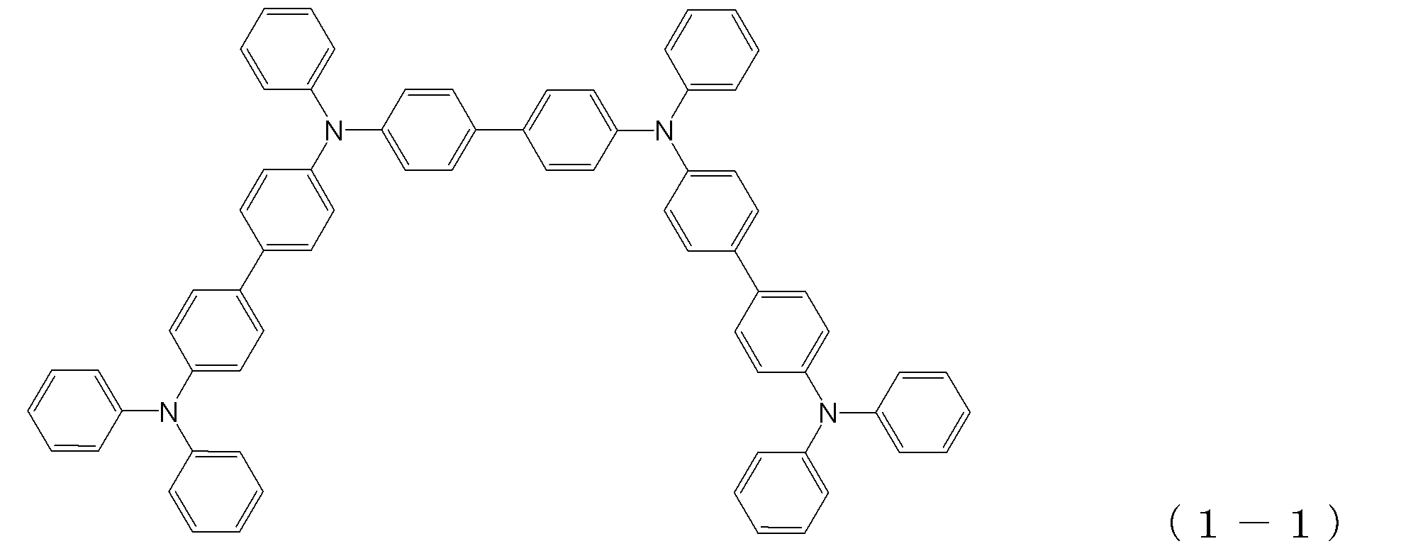
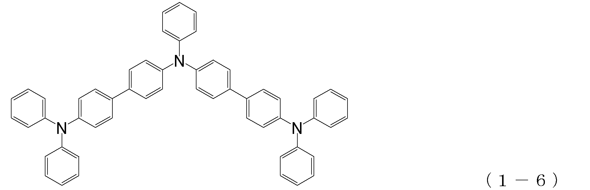
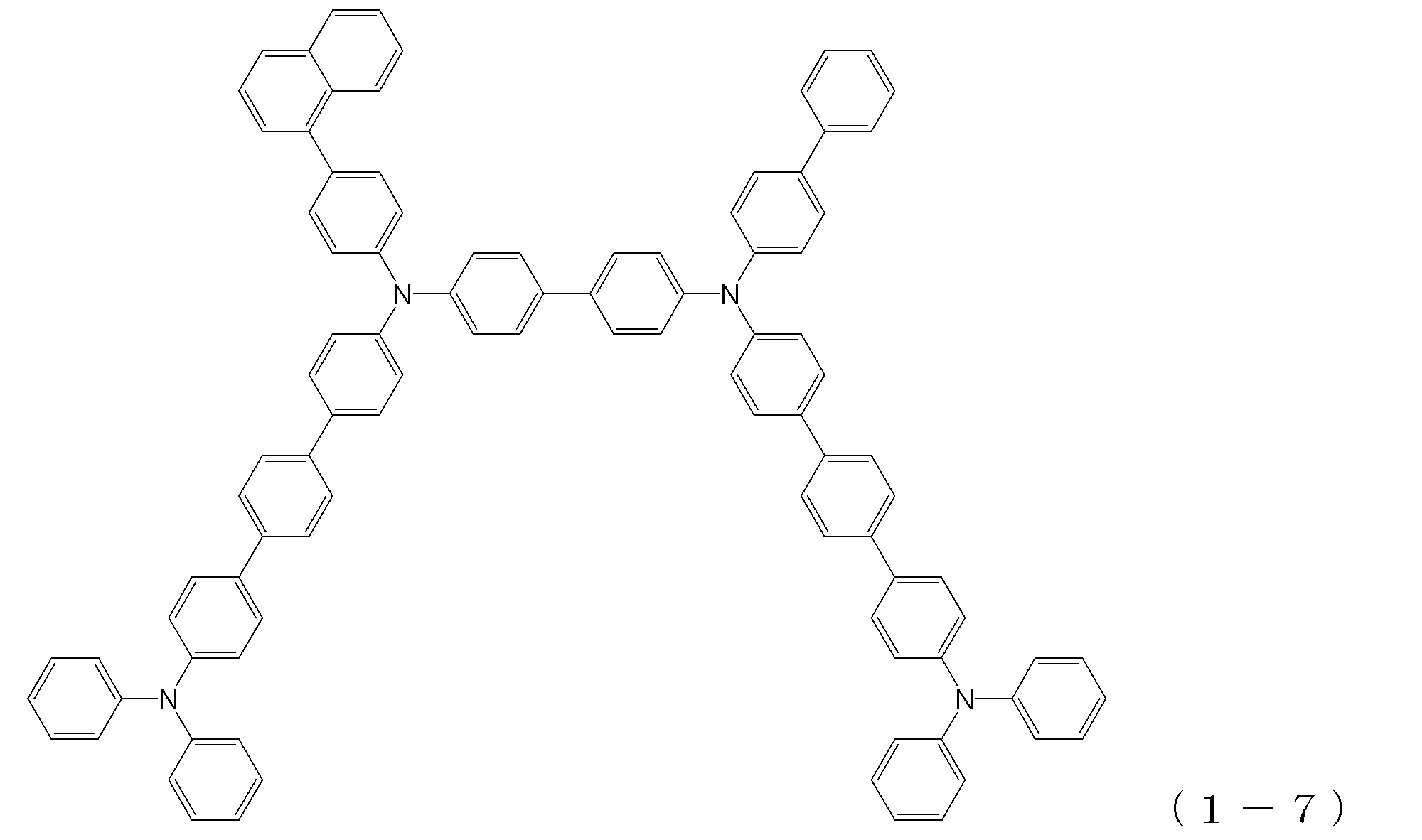
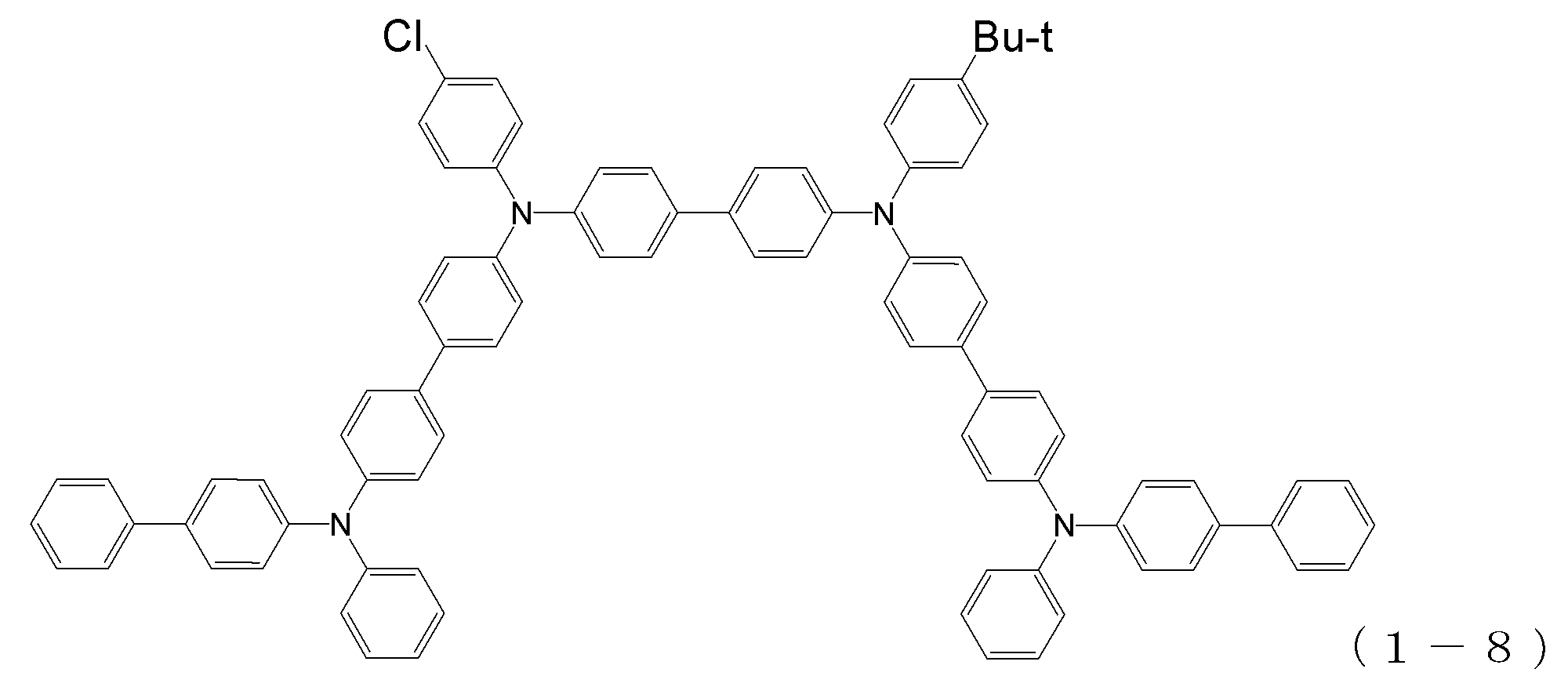
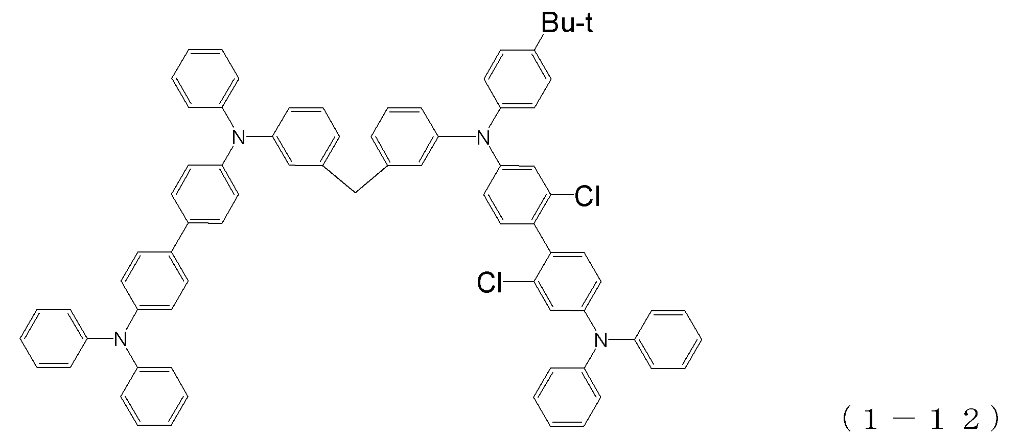
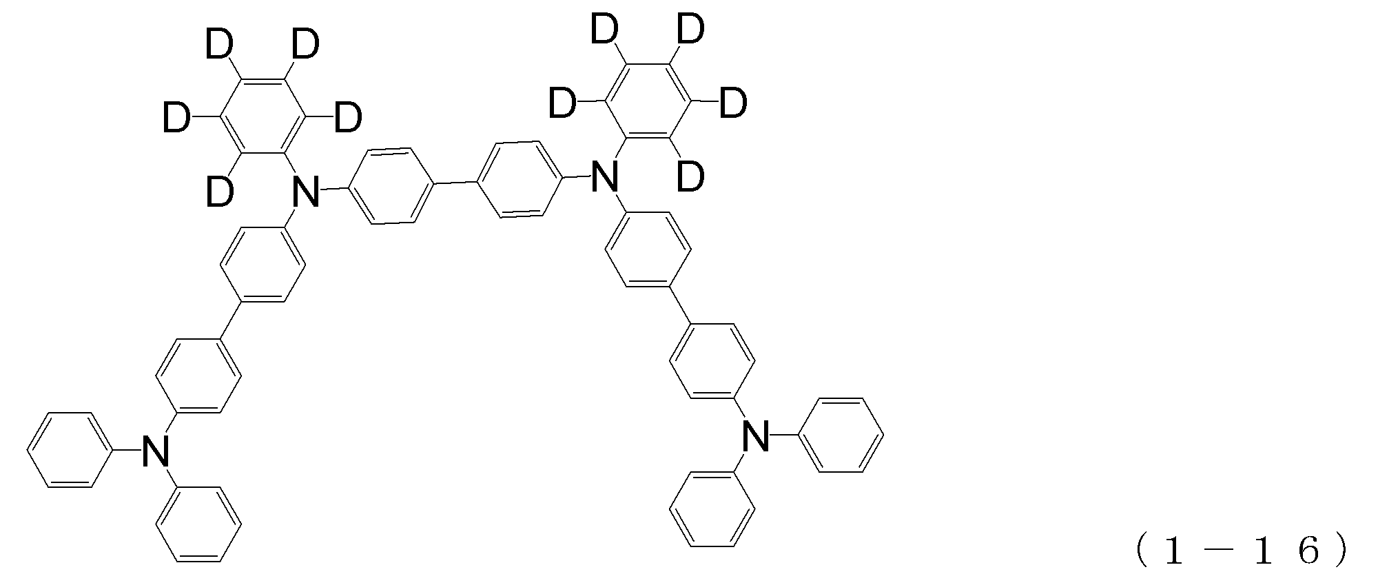
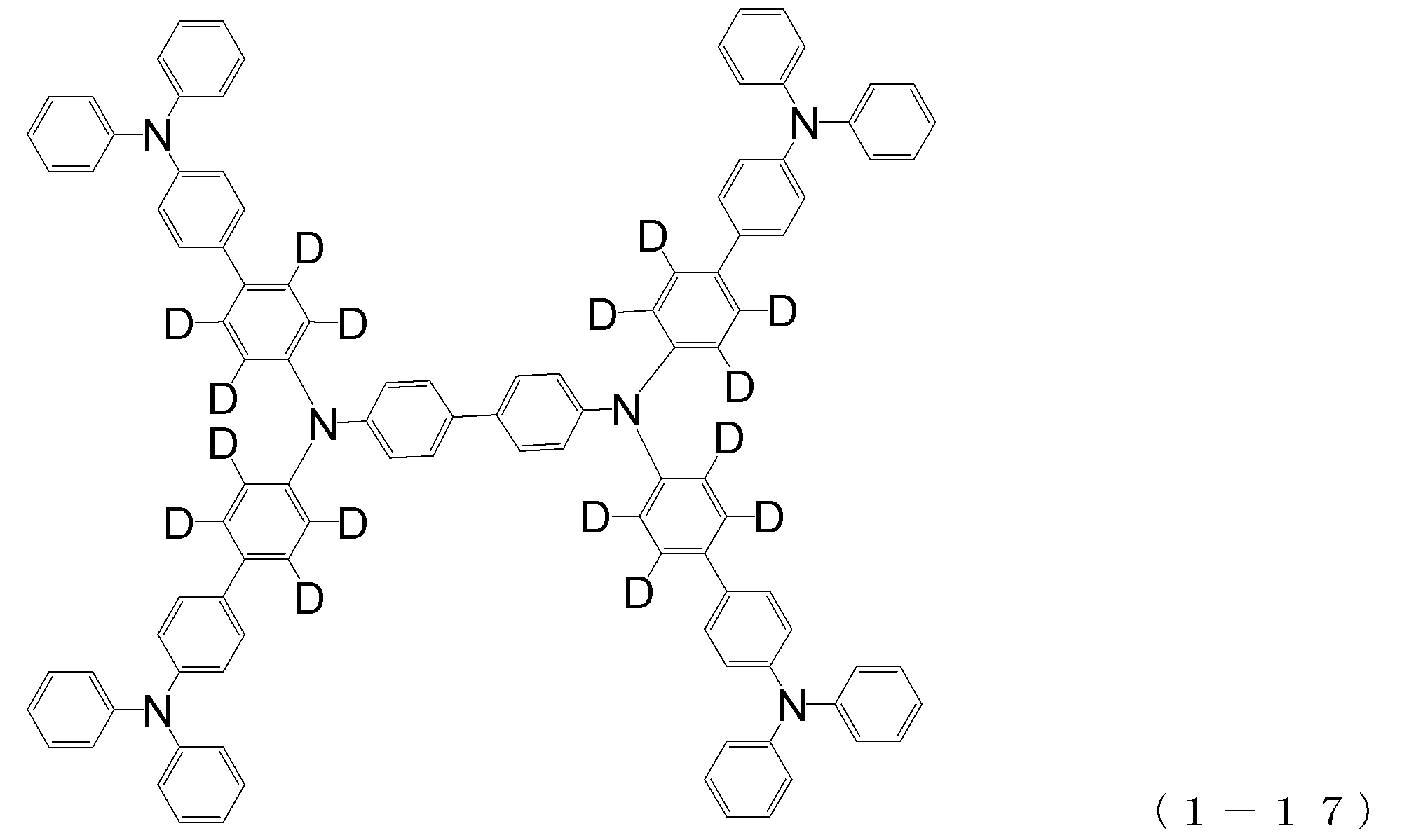
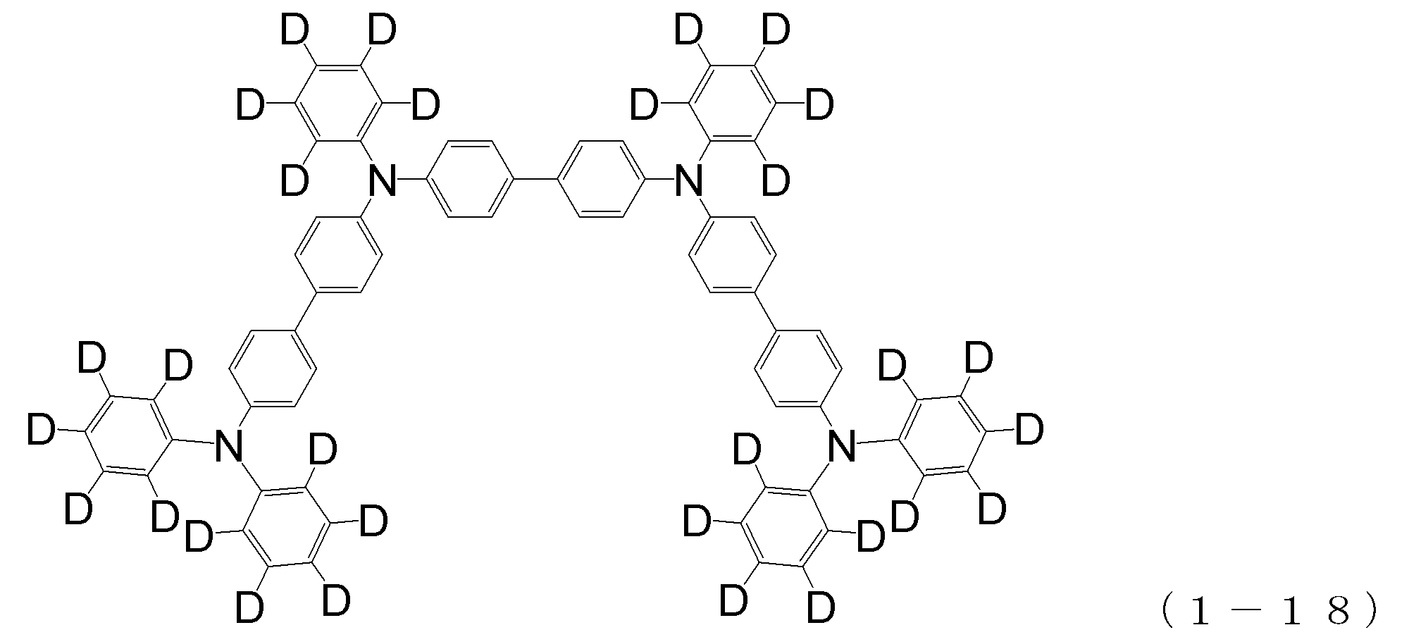
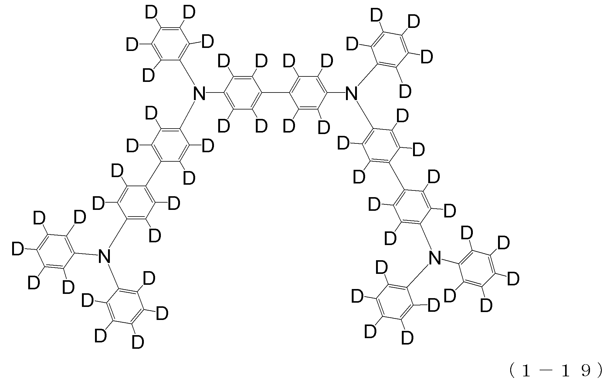
- arylamine compound (X) having three or more triphenylamine skeletons used in the present invention include the following compounds (1-1) to (1-20).
- the triarylamine (having four triphenylamine skeletons) represented by the above general formula (1) is particularly preferable.
- Arylamine compound (Y) The arylamine compound (Y) used in combination with the above-described arylamine compound (X) has two triphenylamine skeletons and is not limited thereto.
- the following general formula (2) It is represented by
- r 13 to r 18 represent the number of groups r 13 to r 18 that can be bonded to the benzene ring in the molecule, and r 13 , r 14 , r 17 and r 18 are , 0 to 5 and r 15 and r 16 each represents an integer of 0 to 4. That is, when the values of r 13 to r 18 are 0, it means that the groups r 13 to r 18 are not bonded to the benzene ring.
- R 13 to R 18 may be the same or different and each includes a deuterium atom, a fluorine atom, a chlorine atom, a cyano group, a trifluoromethyl group, an unsubstituted alkyl group having 1 to 6 carbon atoms, or 1 to 6 carbon atoms.
- those having a plurality of R 13 to R 18 may be bonded to each other to form a ring.
- the unsubstituted alkyl group having 1 to 6 carbon atoms or the unsubstituted alkenyl group having 2 to 6 carbon atoms may be linear or branched.
- R 1 It includes the same alkyl and alkenyl groups as those exemplified for ⁇ R 12.
- Specific examples of the aromatic hydrocarbon group or the aromatic heterocyclic group include the same groups as in R 1 to R 12 .
- the above alkenyl group, aromatic hydrocarbon group and aromatic heterocyclic group may have a substituent, and such a substituent may be the same group as the substituents mentioned for R 1 to R 12. Can be mentioned.
- a plurality of groups R 13 to R 18 when bonded to each other to form a ring, they may be bonded to each other via a single bond to form a ring or have a substituent. And may be bonded to each other via a methylene group, an oxygen atom or a sulfur atom which may be formed to form a ring. In particular, it is preferable that they are bonded to each other via a dimethylmethylene group to form a ring.
- At least one of R 13 to R 18 is a deuterium atom or a substituent containing a deuterium atom (for example, an alkenyl group having a deuterium atom as a substituent, an aromatic hydrocarbon group, and an aromatic heterocyclic group). ) Is preferable.
- a 4 corresponds to a bonding portion between triphenylamine skeletons, and represents a single bond or a divalent hydrocarbon group.
- the divalent hydrocarbon group is represented by the structural formulas (B) to (F).
- TPD N, N′-diphenyl-N, N′-di (m-tolyl) benzidine
- NPD N′-diphenyl-N, N′-di ( ⁇ -naphthyl) benzidine
- TAPC 1,1-bis [4- (di-4-tolylamino) phenyl] cyclohexane
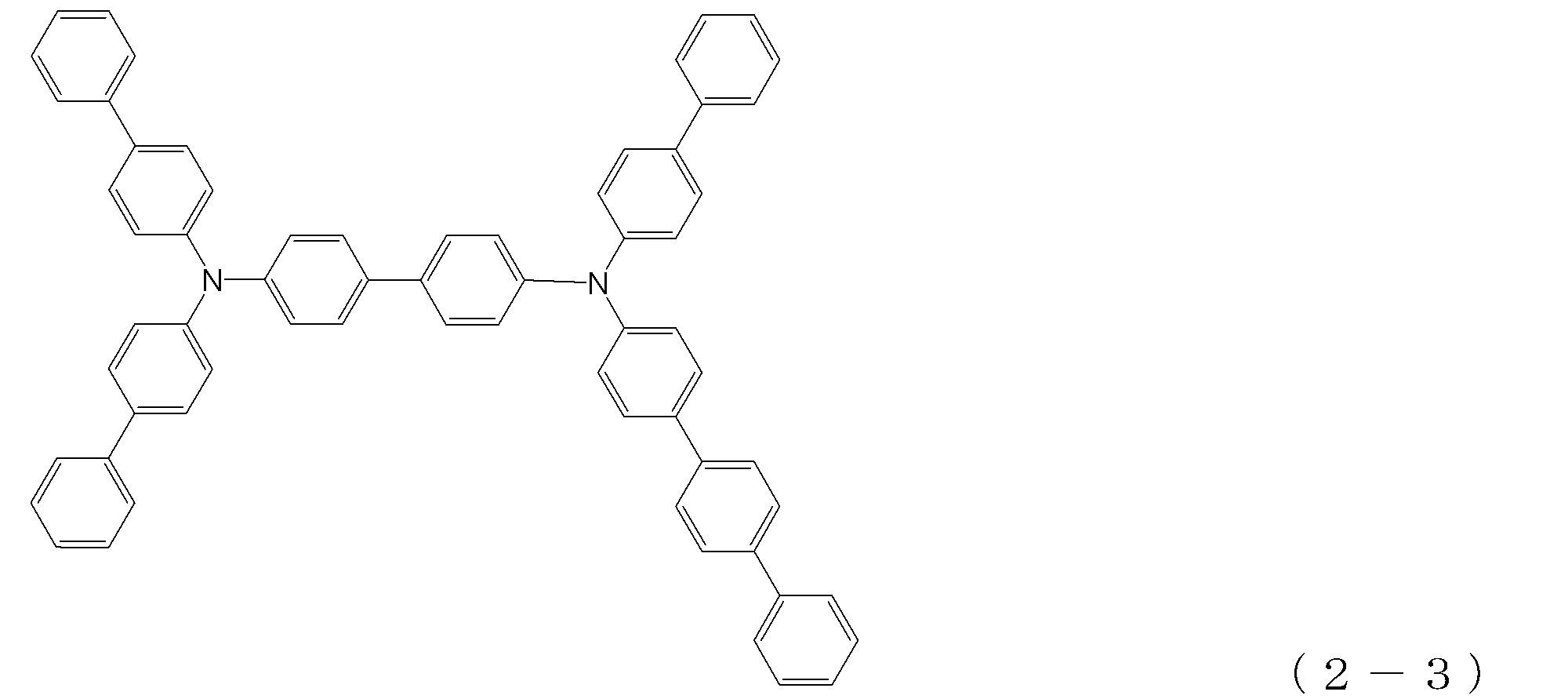
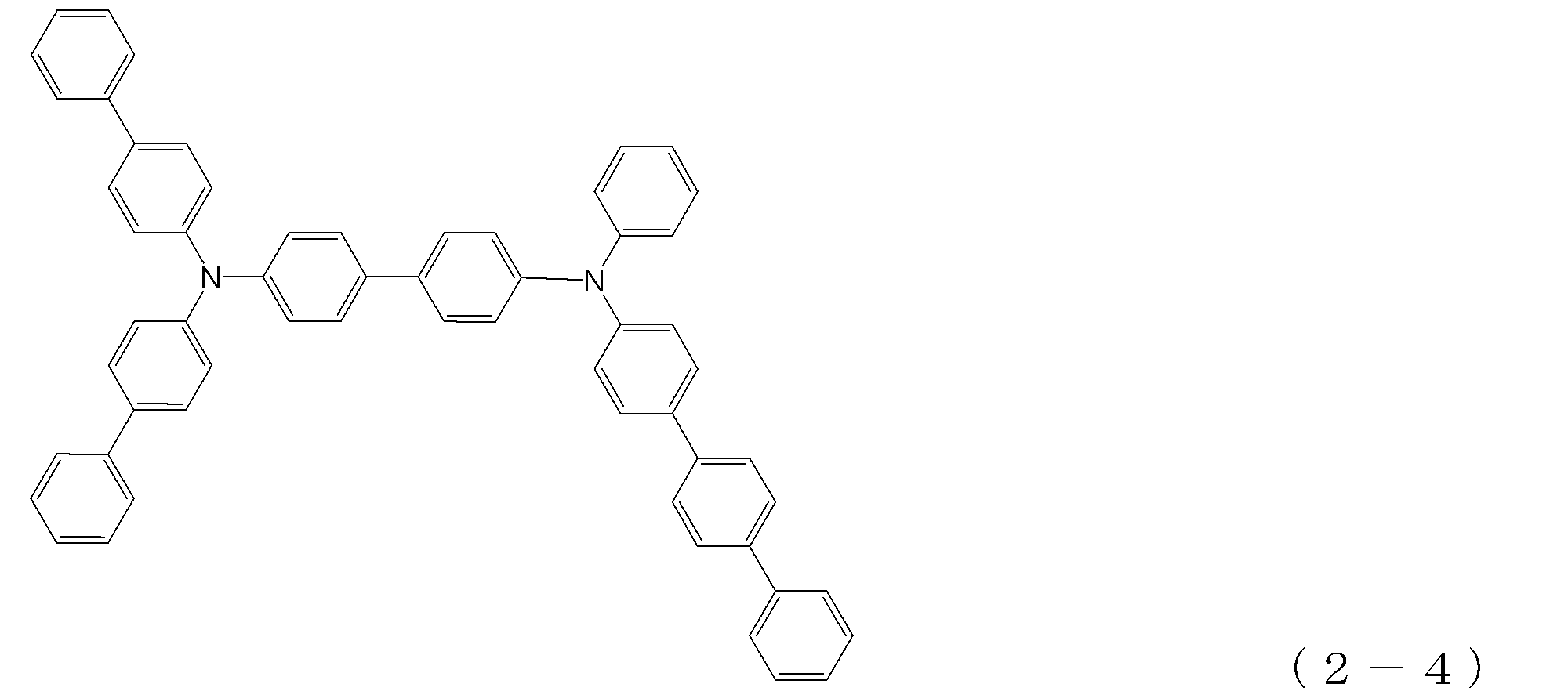
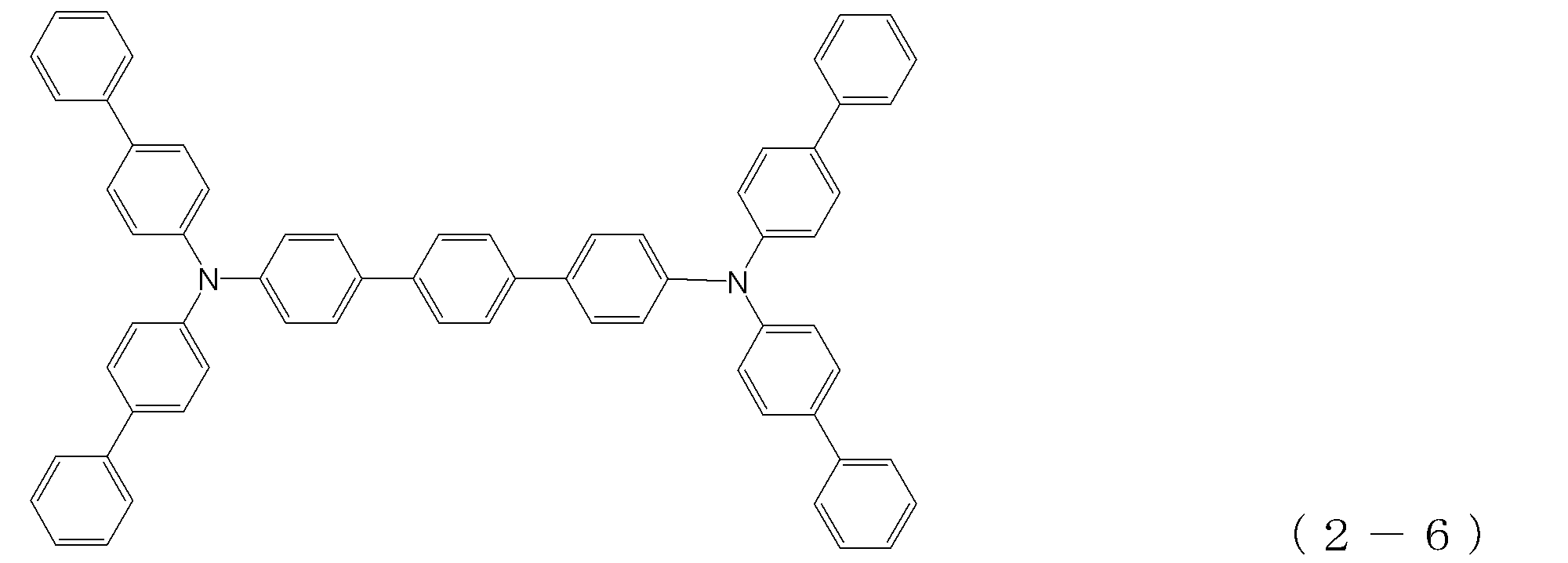
- the following compounds (2′-1) and (2′-2) are also represented as arylamine compounds (Y) having two triphenylamine skeletons: Preferably used.
- arylamine compound (X) and arylamine compound (Y) can be synthesized by a method known per se (see, for example, Patent Documents 7 to 9).
- the hole transport layer of the organic EL device of the present invention contains the two types of arylamine compound (X) and arylamine compound (Y) described above, and such two types of arylamine compound (X). And by using (Y), the moving speed of holes is fast, high luminous efficiency can be secured, and the driving voltage can be lowered. Moreover, since the thin film state of the hole transport layer is stably maintained in addition to the low driving voltage, the life of the organic EL element can be extended.
- the weight ratio (X: Y) of the arylamine compound (X) and the arylamine compound (Y) contained in the hole transport layer is preferably 1: 9 to 6: 4, more preferably Is from 1: 9 to 4: 6, most preferably from 1: 9 to 2: 8. That is, when the hole transport layer is formed by only one of the compounds, the balance between the hole moving speed and the electron moving speed is lost, and two kinds of arylamine compounds are used in combination. In other words, the higher the luminous efficiency, the lower the drive voltage.
- this hole transport layer may contain a material known per se for forming a conventionally known hole transport layer, and has a laminated structure in which layers formed using known materials are laminated. You may have. For example, a layer doped with trisbromophenylamine hexachloroantimony or the like may be laminated on the layer containing the above two kinds of arylamine compounds as an independent layer.
- the thickness of the hole transport layer containing the two kinds of arylamine compounds as described above is usually about 40 to 60 nm, but the thickness can be emitted at a low driving voltage. For example, even when the thickness is increased to 100 nm or more, an increase in driving voltage can be suppressed. That is, the degree of freedom of the thickness of the hole transport layer is high, and a practical driving voltage can be maintained at a thickness of 20 to 300 nm, particularly 20 to 200 nm, for example.
- Such a hole transport layer is preferably formed by co-evaporation using a mixed gas containing the above-described two kinds of arylamine compound (X) and arylamine compound (Y). It can also be formed by a known method such as a method.
- the light emitting layer is the same as that used in a conventionally known organic EL element, and is formed by a known method such as a vapor deposition method, a spin coating method, an ink jet method or the like depending on the type of the material used.
- the light emitting layer can be formed by using.
- the light emitting layer can be formed using a host material and a dopant material (guest material).
- a host material a thiazole derivative, a benzimidazole derivative, a polydialkylfluorene derivative, or the like can be used in addition to the above light emitting material.
- a dopant material quinacridone, coumarin, rubrene, perylene and derivatives thereof, benzopyran derivatives, rhodamine derivatives, aminostyryl derivatives, and the like can be used.
- a phosphorescent emitter can be used as the guest material.
- a phosphorescent emitter of a metal complex such as iridium or platinum can be used.
- a green phosphorescent emitter such as Ir (ppy) 3
- a blue phosphorescent emitter such as FIrpic or FIr6
- a red phosphorescent emitter such as Btp 2 Ir (acac)
- a hole injecting / transporting host material such as 4,4′-di (N-carbazolyl) biphenyl (CBP), carbazole derivatives such as TCTA, mCP and the like can be used.
- Electron transport properties such as bis (triphenylsilyl) benzene (UGH2), 2,2 ′, 2 ′′-(1,3,5-phenylene) -tris (1-phenyl-1H-benzimidazole) (TPBI)
- UHM2 bis (triphenylsilyl) benzene
- TPBI 1,3,5-phenylene
- Host materials can also be used. By using such a host material, a high-performance organic EL element can be produced.
- the host material of the phosphorescent emitter is preferably doped by co-evaporation in the range of 1 to 30 weight percent with respect to the entire light emitting layer.
- the light emitting layer is not limited to a single layer structure, and may have a laminated structure in which layers formed using the various compounds described above are laminated.
- the electron transport layer may be formed per se from known electron-transporting materials, other metal complexes of quinolinol derivatives such as Alq 3, zinc, beryllium, various metal complexes such as aluminum, triazole derivatives, triazine derivatives, oxa Diazole derivatives, thiadiazole derivatives, carbodiimide derivatives, quinoxaline derivatives, phenanthroline derivatives, silole derivatives, and the like can be used.
- quinolinol derivatives such as Alq 3
- zinc beryllium
- various metal complexes such as aluminum, triazole derivatives, triazine derivatives, oxa Diazole derivatives, thiadiazole derivatives, carbodiimide derivatives, quinoxaline derivatives, phenanthroline derivatives, silole derivatives, and the like can be used.
- such an electron transport layer is formed by a known method such as a vapor deposition method, a spin coating method, or an ink jet method, depending on the type of material used.
- a known method such as a vapor deposition method, a spin coating method, or an ink jet method, depending on the type of material used.
- Such an electron transport layer is not limited to a single layer structure, and may have a stacked structure in which layers formed using the various compounds described above are stacked.
- a metal having a low work function such as aluminum, or an alloy having a lower work function such as a magnesium silver alloy, a magnesium indium alloy, or an aluminum magnesium alloy is used as an electrode material.
- the organic EL device of the present invention may have other layers as necessary as long as it has the above-mentioned basic structure.
- a hole injection layer can be provided between the anode and the hole transport layer, and an electron blocking layer can be provided between the hole transport layer and the light emitting layer.
- a hole blocking layer can be provided between the light emitting layer and the electron transport layer.
- an electron injection layer can be provided between the electron transport and the cathode.
- These hole injection layer, electron blocking layer, hole blocking layer and electron injection layer may be formed of materials known per se, depending on the type of material used, vapor deposition method, spin coating method, It is formed by a known method such as an ink jet method.
- the hole injection layer formed between the anode and the hole transport layer is preferably formed of the above-described arylamine compound (X). That is, this arylamine compound (X) has a very high hole mobility.
- Electron blocking layer As a material for forming the electron blocking layer, various compounds having an electron blocking property can be used, and the following carbazole derivatives are typical. 4,4 ′, 4 ′′ -tri (N-carbazolyl) triphenylamine (TCTA); 9,9-bis [4- (carbazol-9-yl) phenyl] fluorene; 1,3-bis (carbazol-9-yl) benzene (mCP); 2,2-bis (4-carbazol-9-ylphenyl) adamantane (Ad-Cz); In addition to the above carbazole derivatives, a triphenylsilyl group represented by 9- [4- (carbazol-9-yl) phenyl] -9- [4- (triphenylsilyl) phenyl] -9H-fluorene is also included. A compound having a triarylamine skeleton in the molecule can also be used as a material for forming an electron blocking layer.
- TCTA
- the hole blocking layer includes various metal complexes of phenanthroline derivatives such as bathocuproine (BCP), quinolinol derivatives such as aluminum (III) bis (2-methyl-8-quinolinato) -4-phenylphenolate (BAlq), It is formed of a compound having a hole blocking action such as a rare earth complex, a triazole derivative, a triazine derivative, or an oxadiazole derivative.
- BCP bathocuproine
- quinolinol derivatives such as aluminum (III) bis (2-methyl-8-quinolinato) -4-phenylphenolate (BAlq)
- Electron injection layer can be formed using an alkali metal salt such as lithium fluoride or cesium fluoride, an alkaline earth metal salt such as magnesium fluoride, or a metal oxide such as aluminum oxide.
- an alkali metal salt such as lithium fluoride or cesium fluoride
- an alkaline earth metal salt such as magnesium fluoride
- a metal oxide such as aluminum oxide.
- hole injection layer, electron blocking layer, hole blocking layer, and electron injection layer described above may each have a single-layer structure or may be formed of a plurality of layers.
- the weight ratio of the two compounds is calculated from the deposition rate (film formation rate) when each compound is used alone and deposition is performed under the same conditions.
- the organic EL element having the structure shown in FIG. 1 was produced by the following procedure. That is, this organic EL element is formed on a glass substrate 1 with a transparent anode 2 (ITO electrode), a hole injection layer 3, a hole transport layer 4, a light emitting layer 5, an electron transport layer 6, an electron injection layer 7, a cathode (aluminum). Electrode) 8 has a structure provided in order by vapor deposition.
- ITO electrode transparent anode 2
- Electrode 8 has a structure provided in order by vapor deposition.
- the glass substrate 1 on which a 150 nm-thick ITO (Indium Tin Oxide) film is formed is subjected to ultrasonic cleaning in isopropyl alcohol for 20 minutes and then dried on a hot plate heated to 200 ° C. for 10 minutes. It was. Then, after performing UV ozone treatment for 5 minutes, this glass substrate with ITO was attached in a vacuum evaporation machine, and pressure was reduced to 0.001 Pa or less. Subsequently, a hole injection layer 3 having a thickness of 20 nm was formed so as to cover the transparent anode 2 by vapor deposition using the following compound (1-1).
- ITO Indium Tin Oxide
- the following compound (1-1) and the following compound (2-1) as the hole transport layer 4 are subjected to binary vapor deposition at a vapor deposition rate with a weight ratio of 20:80. And a film thickness of 40 nm.
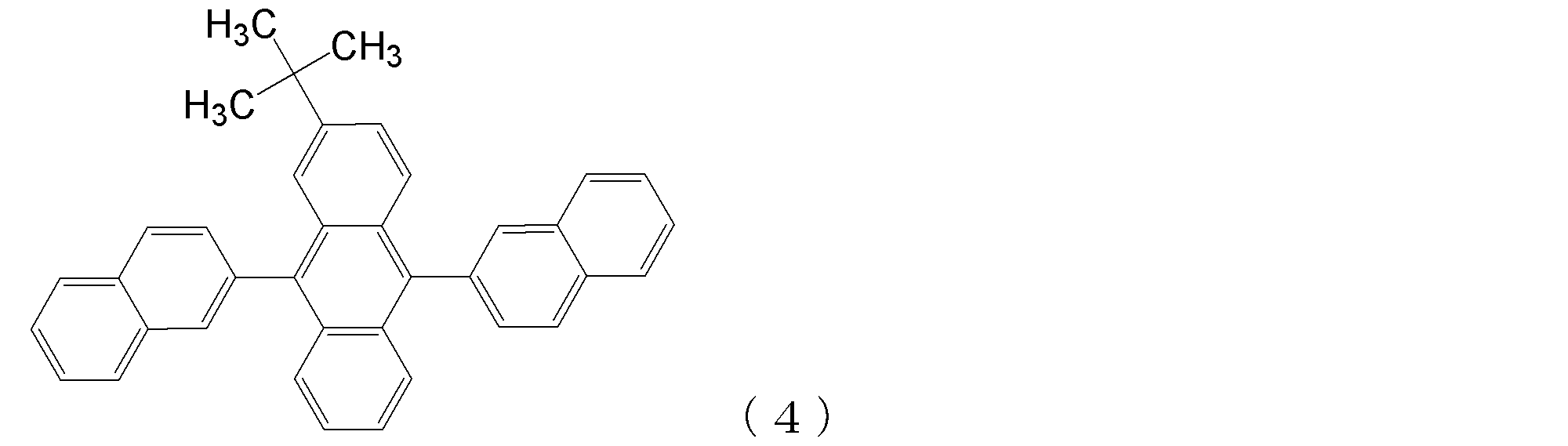
- the following compound (3) and the following compound (4) as the light emitting layer 5 are subjected to binary vapor deposition at a vapor deposition rate of 5:95 to give a film thickness of 30 nm.
- Example 2 In Example 1, the compound (1-1) and the compound (2-1) as the hole transport layer 4 were subjected to binary vapor deposition at a vapor deposition rate with a weight ratio of 10:90, and the film thickness was 40 nm.
- An organic EL element was produced under the same conditions as in Example 1 except that it was formed so as to be. About the produced organic EL element, the characteristic measurement was performed at normal temperature in air
- Example 3 In Example 1, the compound (1-1) and the compound (2-1) as the hole transport layer 4 were subjected to binary vapor deposition at a vapor deposition rate of 40:60 to obtain a film thickness of 40 nm.
- An organic EL element was produced under the same conditions as in Example 1 except that the film was formed as described above. About the produced organic EL element, the characteristic measurement was performed at normal temperature in air
- Example 4 In Example 1, the compound (1-1) and the compound (2-1) as the hole transport layer 4 were subjected to binary deposition at a deposition rate of 60:40 by weight, and the film thickness was 40 nm.
- An organic EL element was produced under the same conditions as in Example 1 except that the film was formed as described above. About the produced organic EL element, the characteristic measurement was performed at normal temperature in air
- Example 1 For comparison, an organic EL device was produced under the same conditions as in Example 1 except that the compound (2-1) was formed to a thickness of 40 nm as the hole transport layer 4 in Example 1. . About the produced organic EL element, the characteristic measurement was performed at normal temperature in air
- Example 2 For comparison, an organic EL device was fabricated under the same conditions as in Example 1, except that the compound 1-1 of the structural formula was formed to a thickness of 40 nm as the hole transport layer 4 in Example 1. did. About the produced organic EL element, the characteristic measurement was performed at normal temperature in air
- Example 3 For comparison, in Example 1, binary deposition of the compound (1-1) and the compound (2-1) as the hole transport layer 4 was performed at a deposition rate with a weight ratio of 80:20. An organic EL element was produced under the same conditions as in Example 1 except that the film thickness was 40 nm. About the produced organic EL element, the characteristic measurement was performed at normal temperature in air
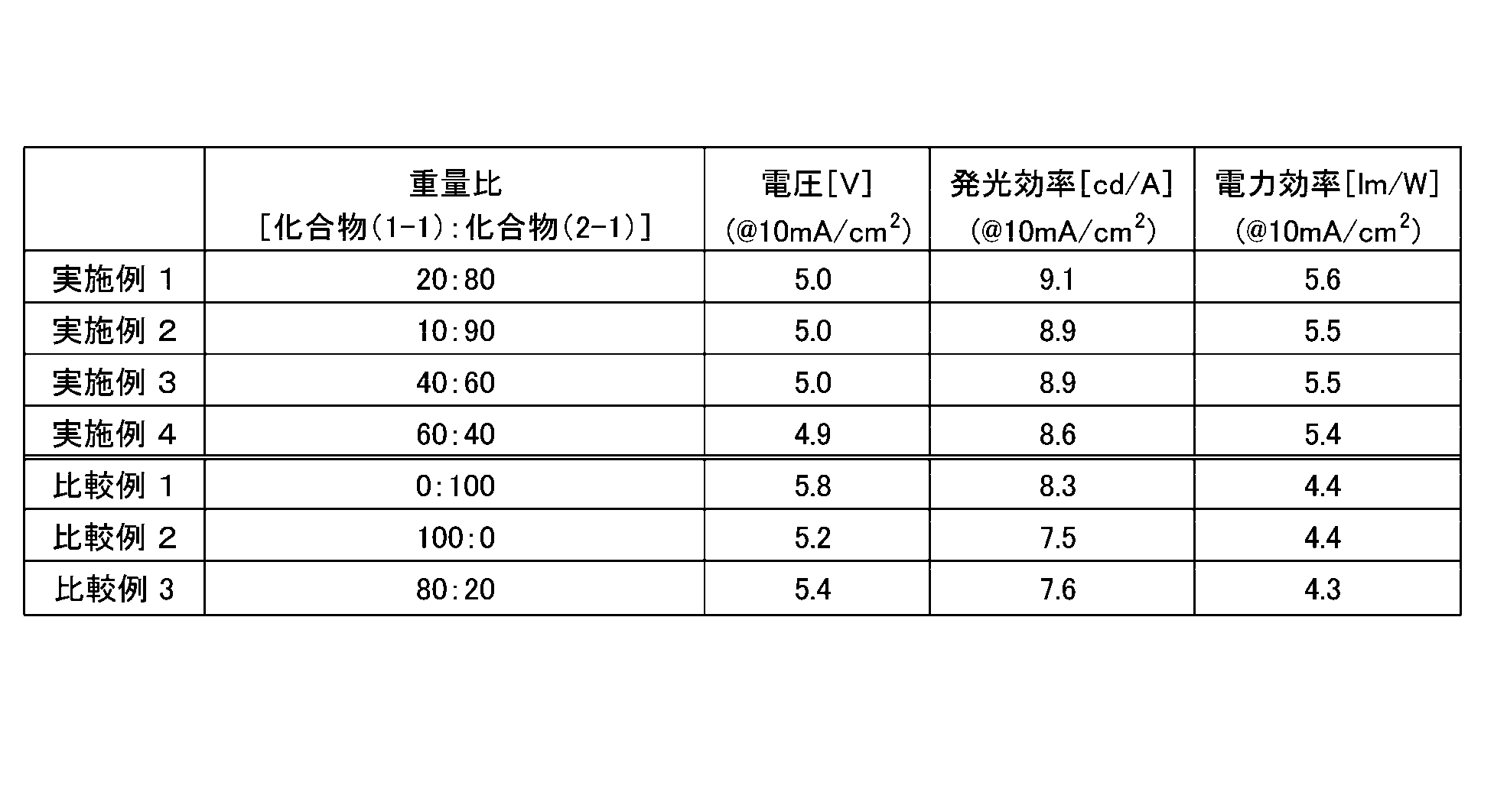
- the driving voltage when a current density of 10 mA / cm 2 was passed was in the case of the elements of Examples 1 to 4 (4.9 to 5.0 V), and the elements of Comparative Examples 1 to 3 In the case of (5.2 to 5.8 V), the voltage was lowered.
- the elements of Examples 1 to 4 (8.6 to 9.1 cd / A) are more than the elements of Comparative Examples 1 to 3 (7.5 to 8.3 cd / A). Therefore, in terms of power efficiency, the devices of Examples 1 to 4 (5.4 to 5.6 lm / W) and the devices of Comparative Examples 1 to 3 (4.3 to 4.4 lm) are improved. / W), the result was greatly improved.
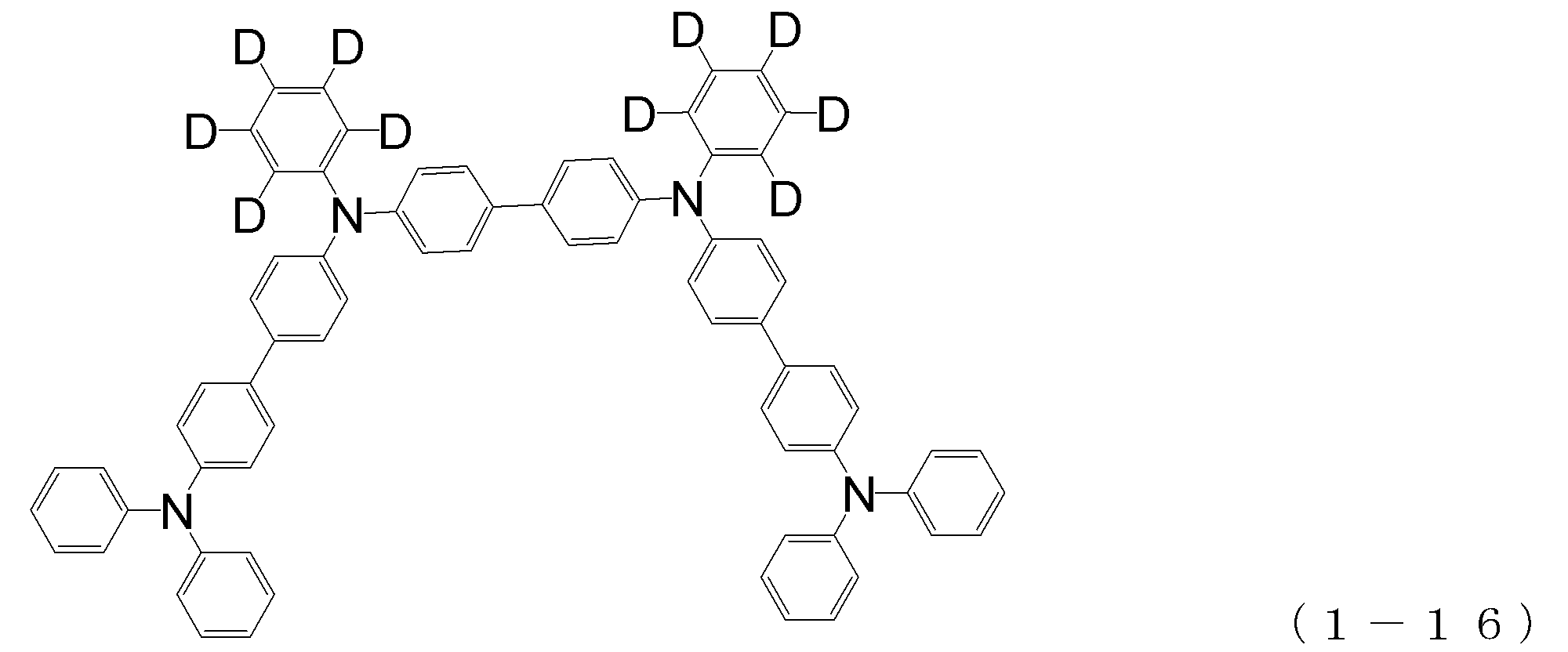
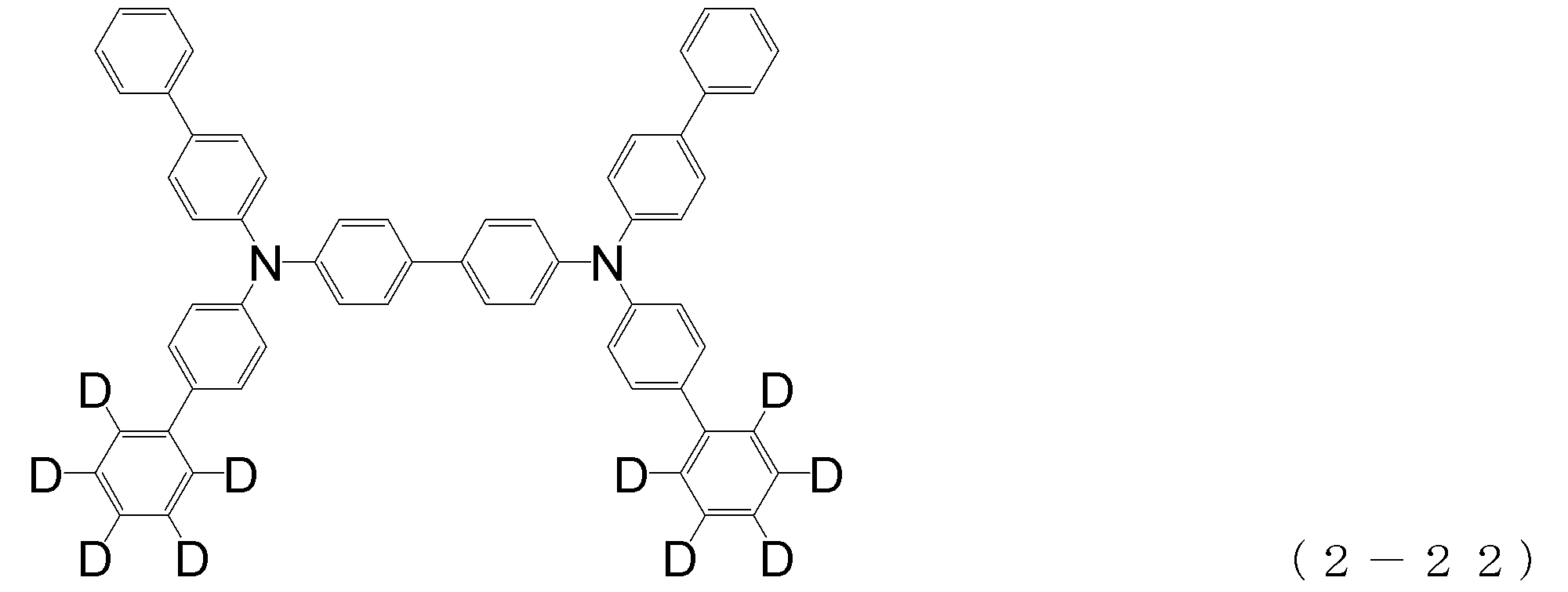
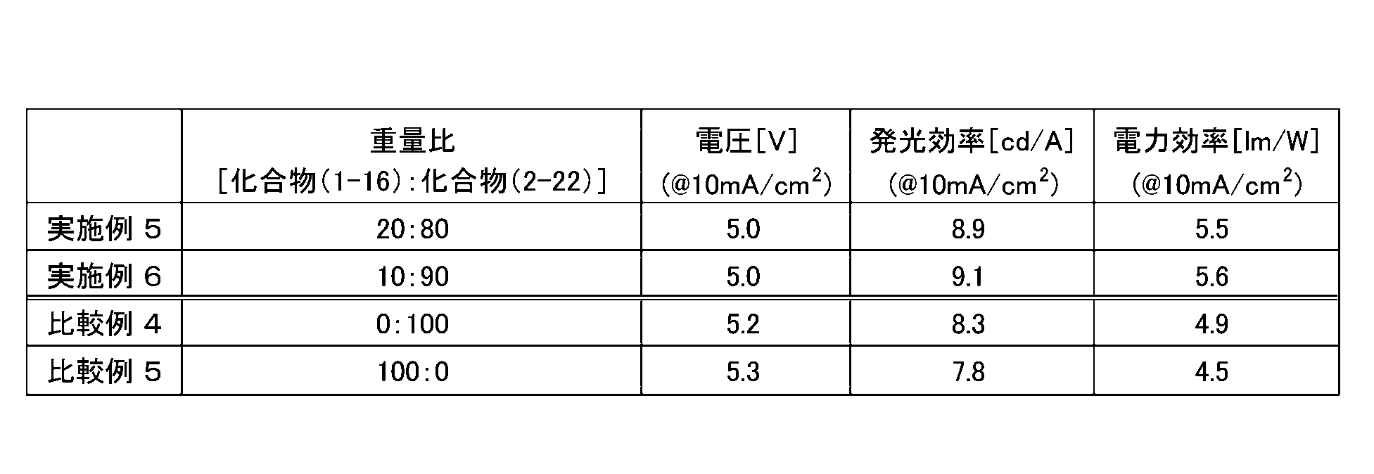
- Example 5 In Example 1, as the hole transport layer 4, the following compound (1-16) and the following compound (2-22) were subjected to binary vapor deposition at a vapor deposition rate of 20:80 to obtain a film thickness of 40 nm. An organic EL element was produced under the same conditions as in Example 1 except that it was formed so as to be. About the produced organic EL element, the characteristic measurement was performed at normal temperature in air
- Example 6 In Example 5, the compound (1-16) and the compound (2-22) as the hole transport layer 4 were subjected to binary vapor deposition at a vapor deposition rate of 10:90, and the film thickness was 40 nm.
- An organic EL element was produced under the same conditions as in Example 5 except that it was formed so as to be. About the produced organic EL element, the characteristic measurement was performed at normal temperature in air
- Example 4 For comparison, an organic EL device was produced under the same conditions as in Example 5, except that in Example 5, the compound (2-22) was formed to a thickness of 40 nm as the hole transport layer 4. . About the produced organic EL element, the characteristic measurement was performed at normal temperature in air
- Example 5 For comparison, an organic EL device was produced under the same conditions as in Example 5 except that in Example 5, the compound (1-16) was formed to a thickness of 40 nm as the hole transport layer 4. . About the produced organic EL element, the characteristic measurement was performed at normal temperature in air
- the driving voltage when a current density of 10 mA / cm 2 was passed was the case of the elements of Examples 5 to 6 (5.0 V) and the case of the elements of Comparative Examples 4 to 5 (5 .2 to 5.3 V).
- the elements of Examples 5 to 6 (8.9 to 9.1 cd / A) are more than the elements of Comparative Examples 4 to 5 (7.8 to 8.3 cd / A). Therefore, in terms of power efficiency, the devices of Examples 5 to 6 (5.5 to 5.6 lm / W) and the devices of Comparative Examples 4 to 5 (4.5 to 4.9 lm) are improved. / W), the result was greatly improved.
- Table 3 summarizes the results of measuring element lifetimes using the same organic EL elements as in Example 1, Comparative Example 1 and Comparative Example 2.
- the lifetime of the element is measured by measuring the time when the luminance is attenuated to 95% when the initial luminance is 100% with respect to the light emission luminance when the current amount (W) when emitting light at a luminance of 1000 cd / m 2 is constant. And asked.
- the organic EL device of the present invention improves the carrier balance inside the organic EL device by combining two specific types of arylamine compounds, and has a low driving voltage, high luminous efficiency, compared to conventional organic EL devices, It was found that a long-life organic EL element can be realized.
- the organic EL device of the present invention which is a combination of two specific types of arylamine compounds, can improve luminous efficiency and drive voltage, thereby improving the durability of the organic EL device. It has become possible to develop applications for electrical appliances and lighting.
Landscapes
- Chemical & Material Sciences (AREA)
- Organic Chemistry (AREA)
- Engineering & Computer Science (AREA)
- Materials Engineering (AREA)
- Physics & Mathematics (AREA)
- Spectroscopy & Molecular Physics (AREA)
- Manufacturing & Machinery (AREA)
- Electroluminescent Light Sources (AREA)
- Organic Low-Molecular-Weight Compounds And Preparation Thereof (AREA)
Abstract
Description
また発光効率の更なる向上を目的として三重項励起子の利用が試みられ、燐光発光性化合物の利用も検討されている。
一方、正孔輸送材料としては、ベンジジン骨格を含むアリールアミン系材料が用いられてきた(特許文献5参照)。
前記正孔輸送層が、3個以上のトリフェニルアミン骨格が単結合或いは2価の炭化水素基で結合されている分子構造を有するアリールアミン化合物(X)と、2個のトリフェニルアミン骨格が単結合或いは2価の炭化水素基で結合されている分子構造を有するアリールアミン化合物(Y)とを含んでいる有機エレクトロルミネッセンス素子が提供される。
r1~r12は、それぞれ、R1~R12の数を示すものであり、
r1、r2、r5、r8、r11及びr12は、0~5の整数を表し、
r3、r4、r6、r7、r9及びr10は、0~4の整数を表し、
R1~R12は、それぞれ、重水素原子、フッ素原子、塩素原子、
シアノ基、トリフルオロメチル基、炭素原子数1ないし6の無置換アル
キル基、炭素原子数2ないし6の無置換もしくは置換アルケニル基、無
置換もしくは置換芳香族炭化水素基または無置換もしくは置換芳香族複
素環基であり、これらの基の中で同一のベンゼン環に結合しているもの
同士は、互いに結合して環を形成していてもよく、
A1~A3は、それぞれ、単結合或いは下記構造式(B)~(F)で
表される2価の炭化水素基を表す。




r13~r18は、R13~R18の数を示すものであり、r13、
r14、r17及びr18は、0~5の整数であり、r15及びr16
は、0~4の整数を表し、
R13~R18は、それぞれ、重水素原子、フッ素原子、塩素原子、
シアノ基、トリフルオロメチル基、炭素原子数1ないし6の無置換アル
キル基、炭素原子数2ないし6の無置換もしくは置換アルケニル基、無
置換もしくは置換芳香族炭化水素基または無置換もしくは置換芳香族複
素環基であり、これらの基の中で同一のベンゼン環に結合しているもの
同士は、互いに結合して環を形成していてもよく、
A4は、単結合または下記構造式(B)~(F)で表される2価の炭
化水素基を示す。
即ち、このようなアリールアミン化合物(X)及び(Y)が組み合わせて含まれている正孔輸送層は、正孔の移動速度が速く、薄膜状態が安定に維持され且つ優れた耐熱性を示す。
従って、本発明の有機EL素子は、正孔輸送層から発光層への正孔を効率よく注入・輸送でき、高い発光効率を示し、駆動電圧も低く、この結果、長寿命化も実現できる。
以下、この有機EL素子を構成する各層について説明する。
陽極は、透明プラスチック基板(例えばポリエチレンテレフタレート基板)やガラス基板などの透明基板上への蒸着により設けられるものであり、ITOや金のような仕事関数の大きな電極材料により形成される。
既に述べたように、発光層に対して陽極側に位置する正孔輸送層にはトリフェニルアミン骨格を有する2種のアリールアミン化合物(X),(Y)が含まれる。
一方のアリールアミン化合物(X)は、トリフェニルアミン骨格を3個以上有するものであり、これらのトリフェニルアミン骨格は、単結合、或いは2価の炭化水素基(即ち、ヘテロ原子を含まない2価の基)で結合されている。このアリールアミン化合物(X)は、後述するアリールアミン化合物(Y)と比較しても正孔移動度が高い。
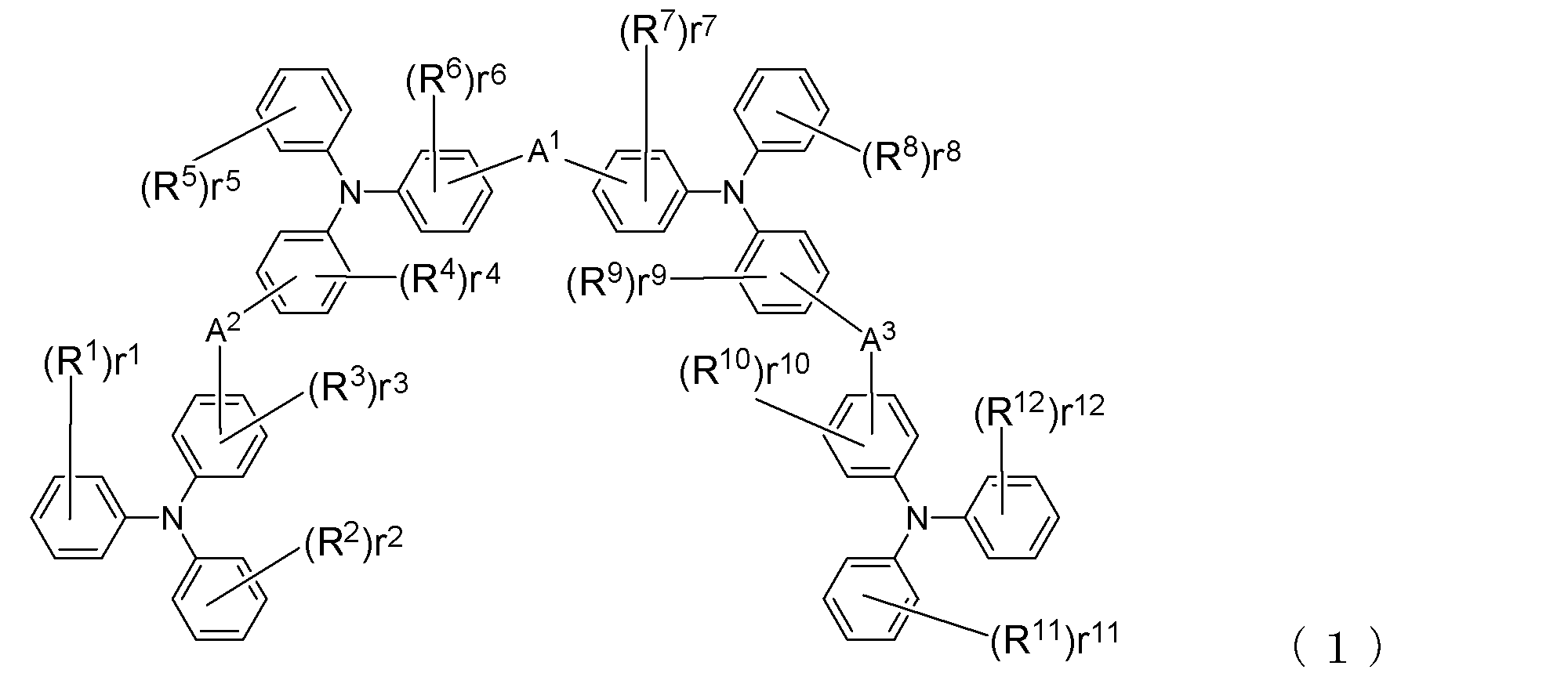
この2価の炭化水素基、即ち、ヘテロ原子を含まない2価の基としては、下記構造式(B)~(F)で表されるものを挙げることができる。





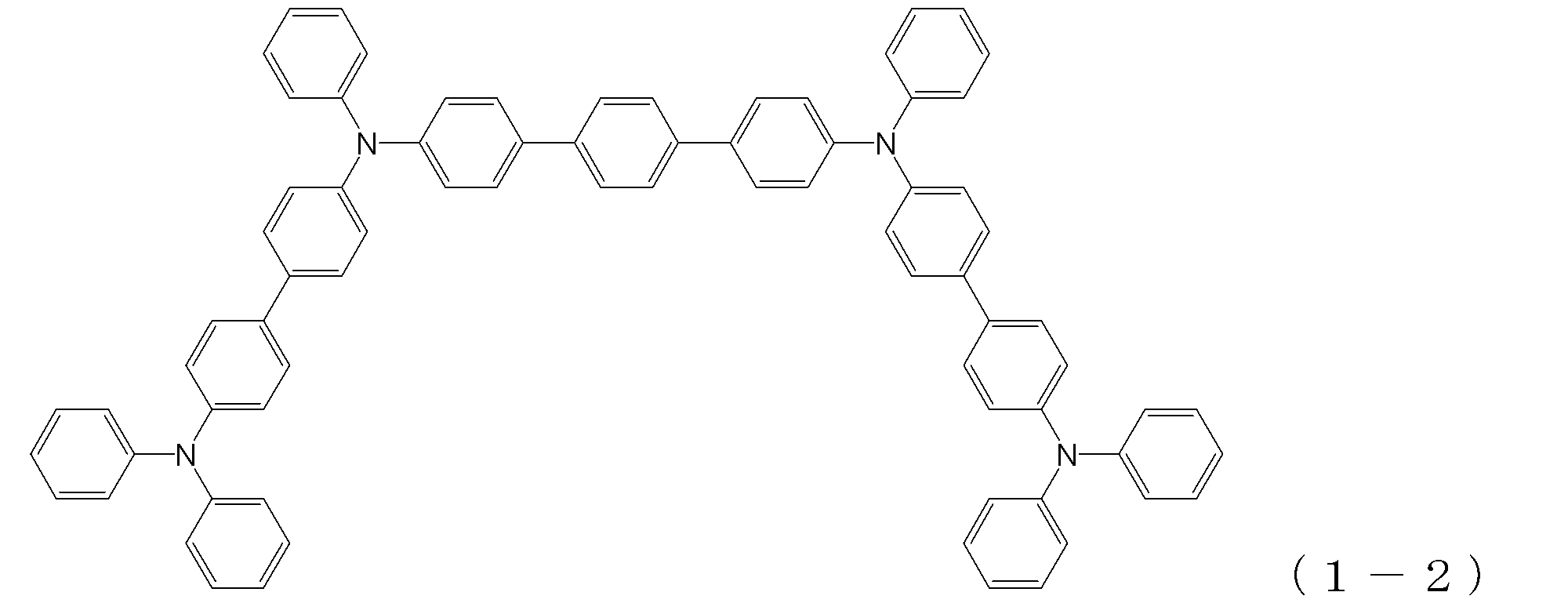
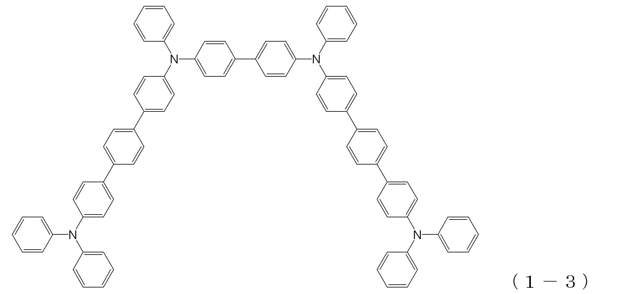
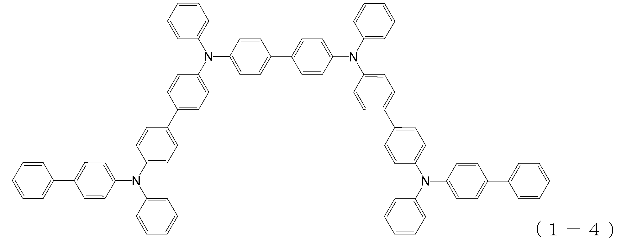
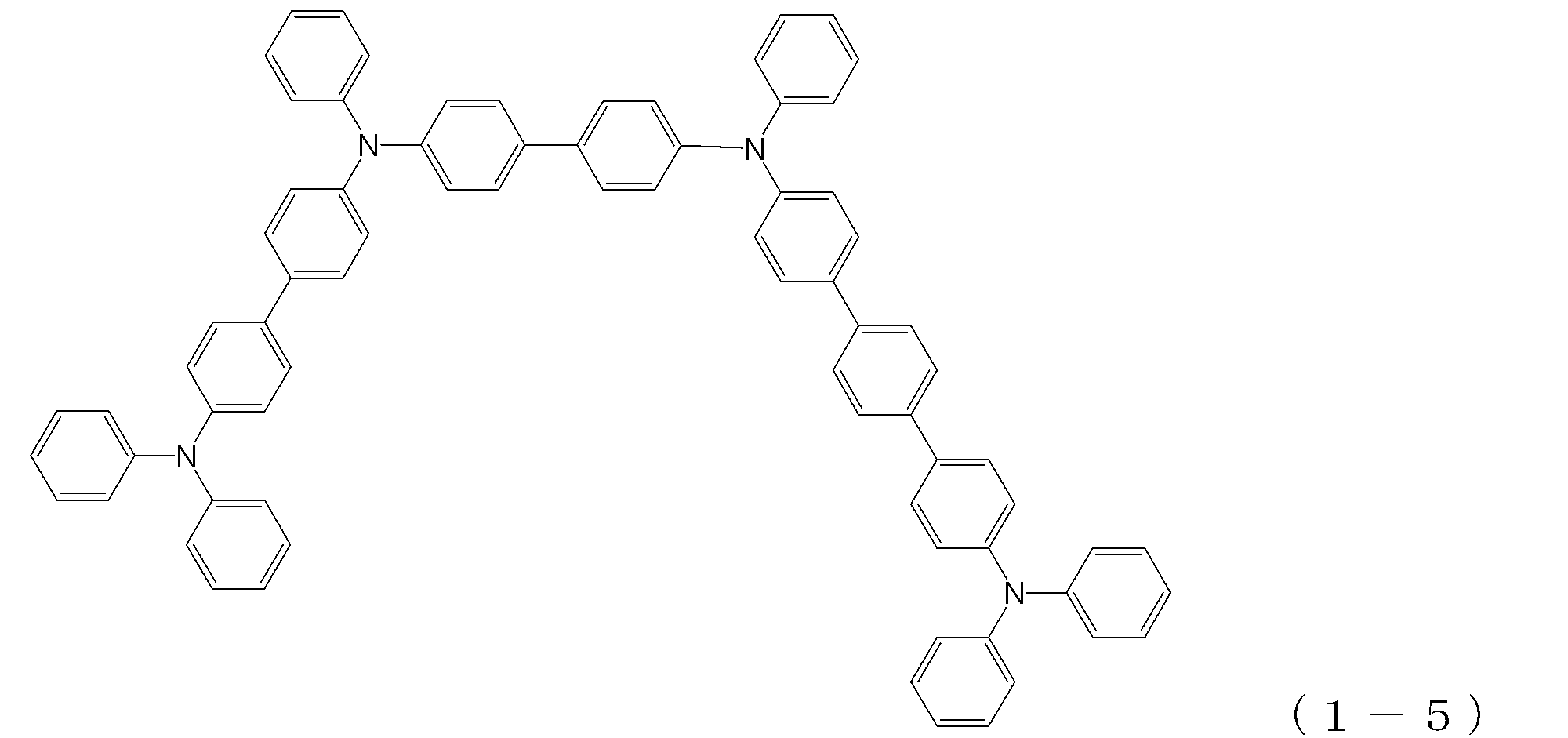




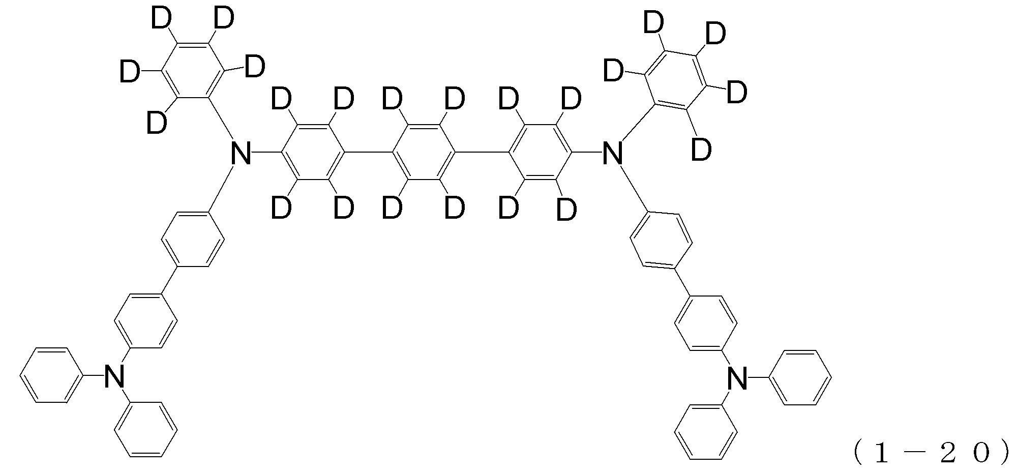
上述したアリールアミン化合物(X)と併用されるアリールアミン化合物(Y)は、トリフェニルアミン骨格を2個有するものであり、これに限定されるものではないが、例えば下記の一般式(2)で表わされる。

芳香族炭化水素基または芳香族複素環基の具体例としては、R1~R12の場合と同様な基をあげることができる。
N,N’-ジフェニル-N,N’-ジ(m-トリル)ベンジジン
(TPD)、
N,N’-ジフェニル-N,N’-ジ(α-ナフチル)ベンジジン
(NPD)、
1,1-ビス[4-(ジ-4-トリルアミノ)フェニル]シクロヘキサン
(TAPC)、
及び、以下に挙げる(2-1)~(2-26)の化合物を例示することができる。



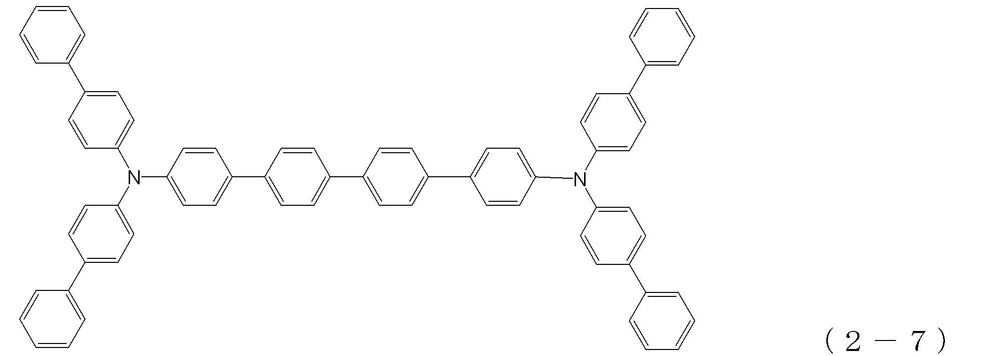


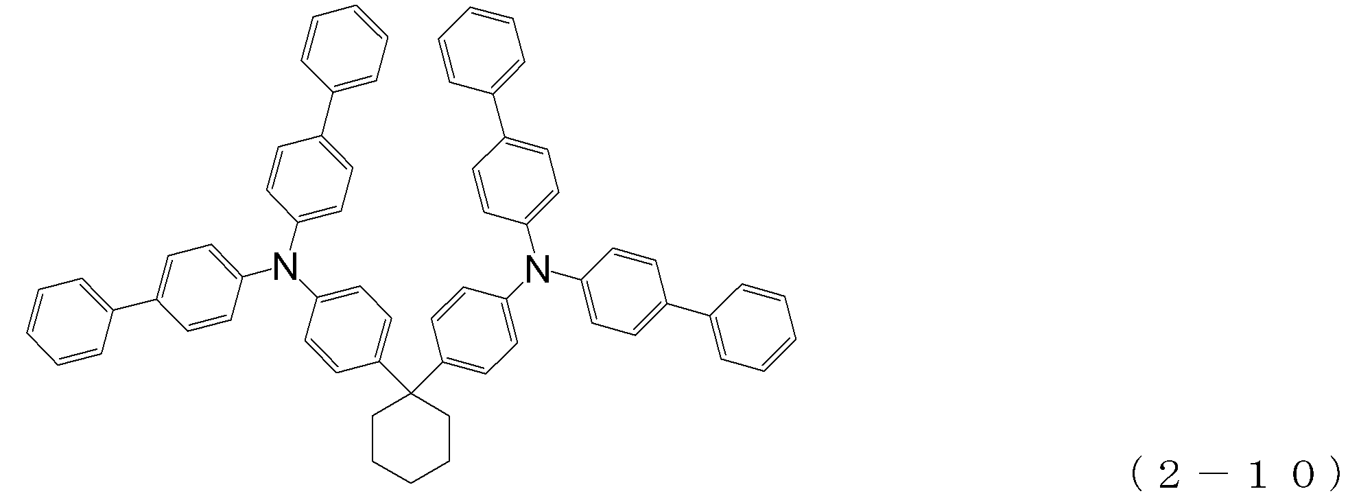
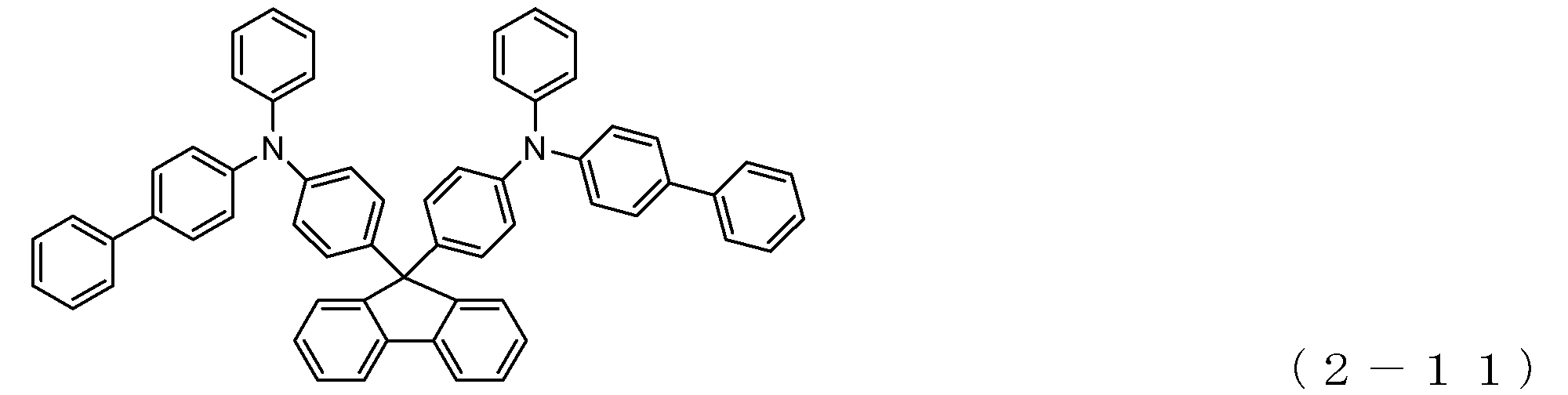
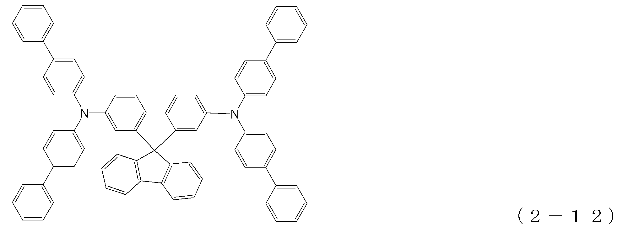
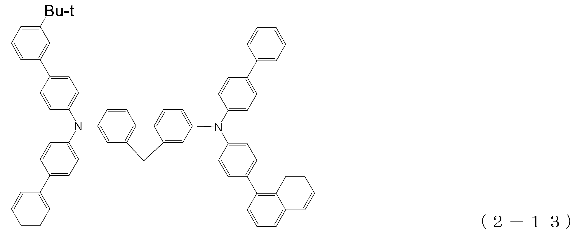


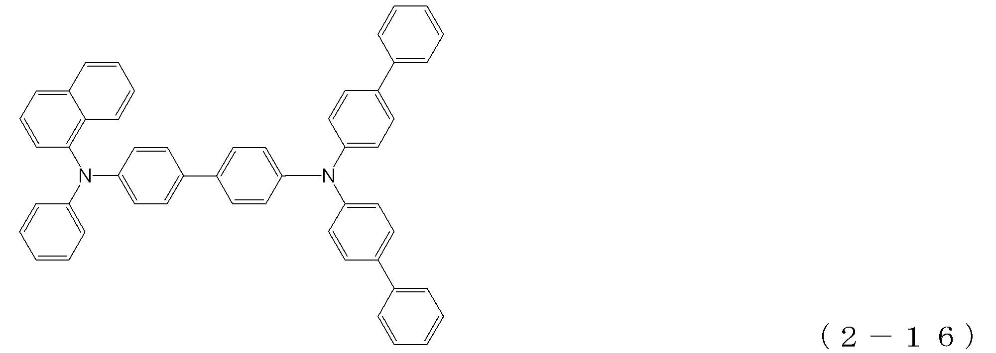
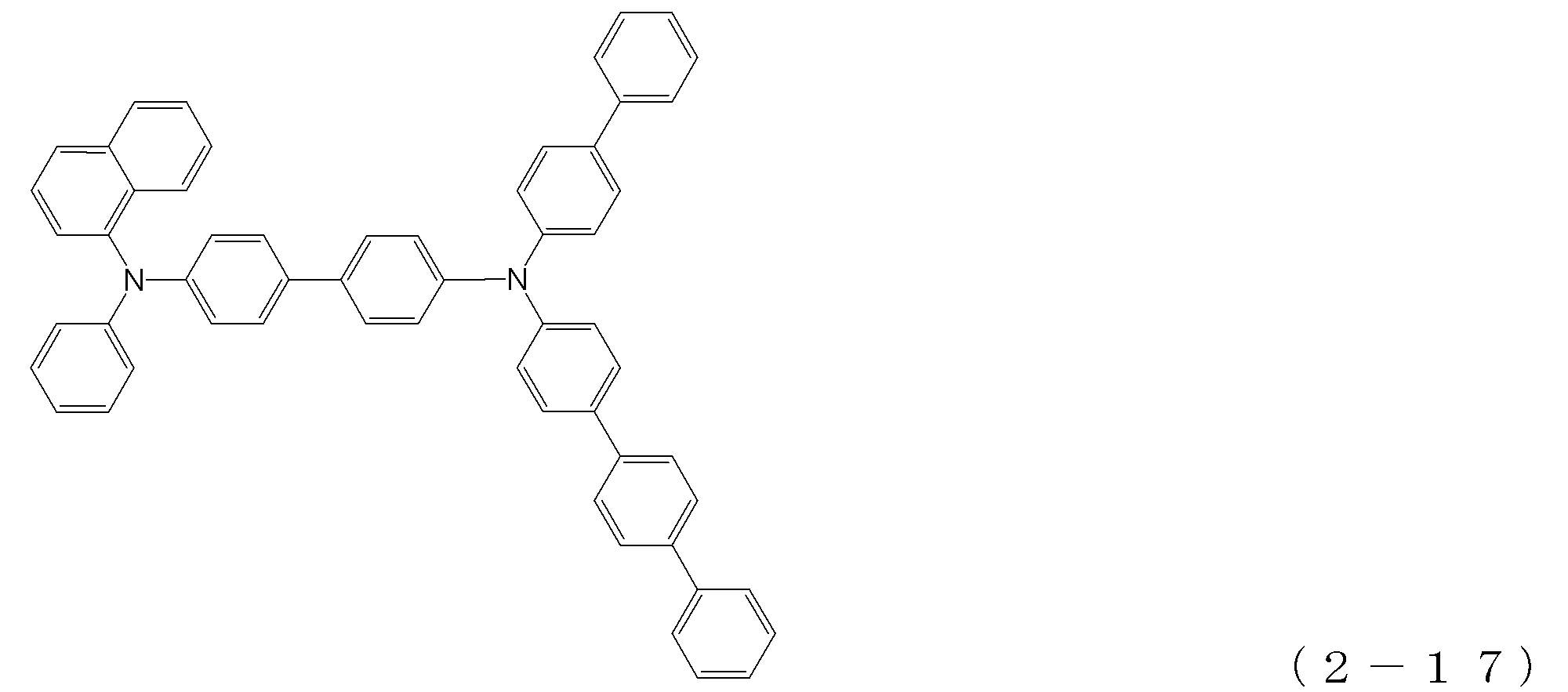
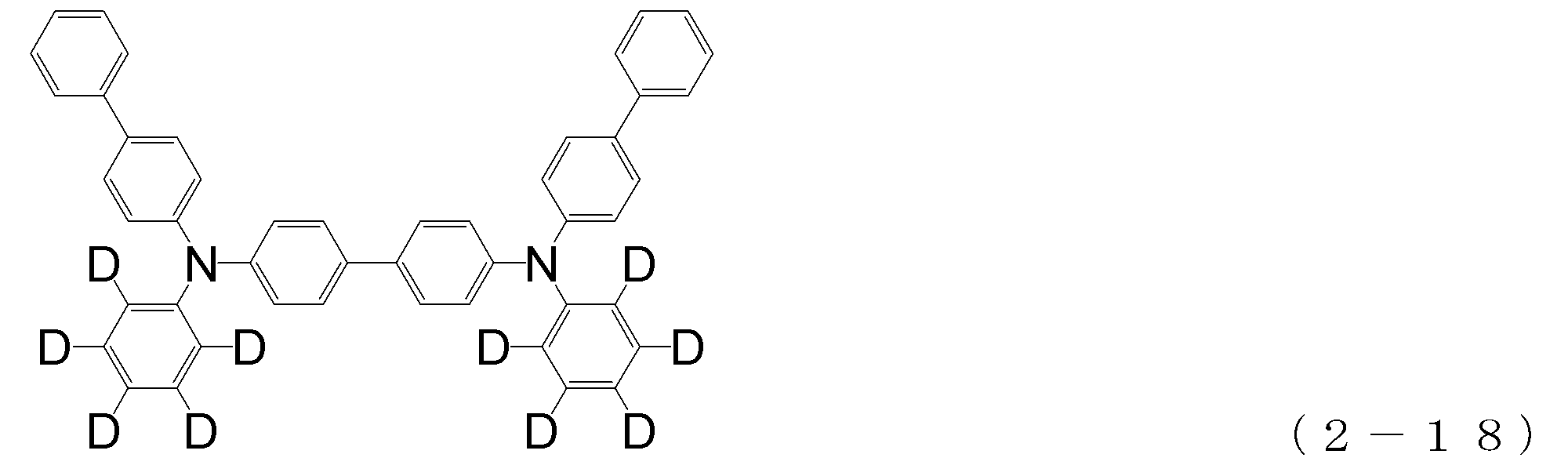
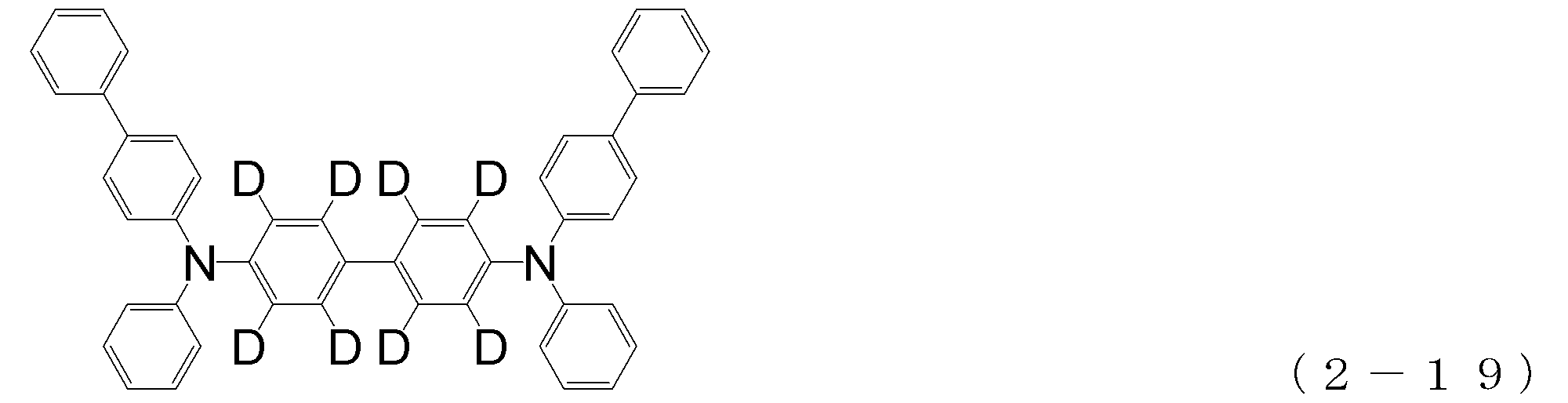
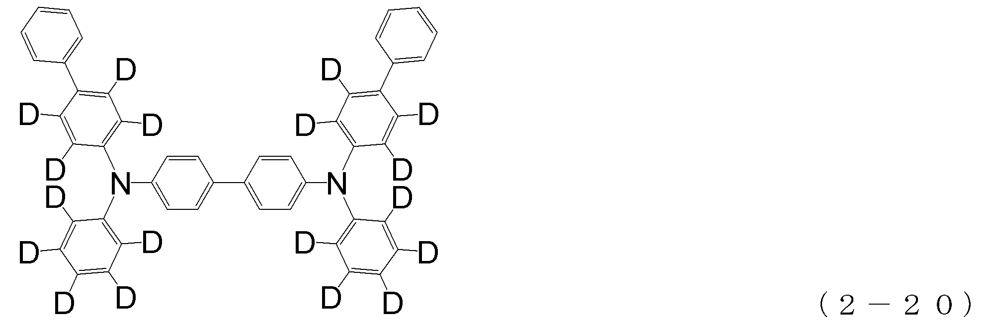


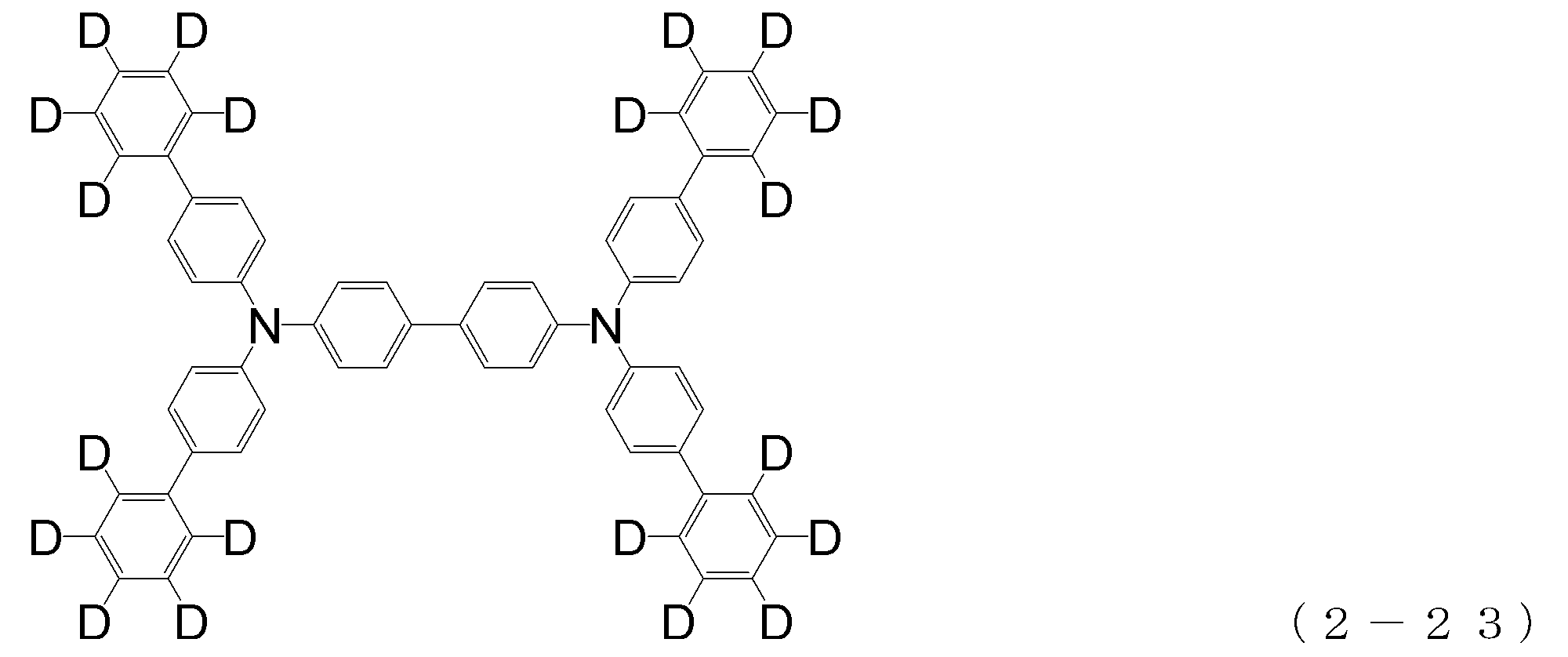
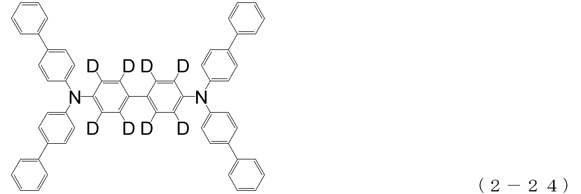
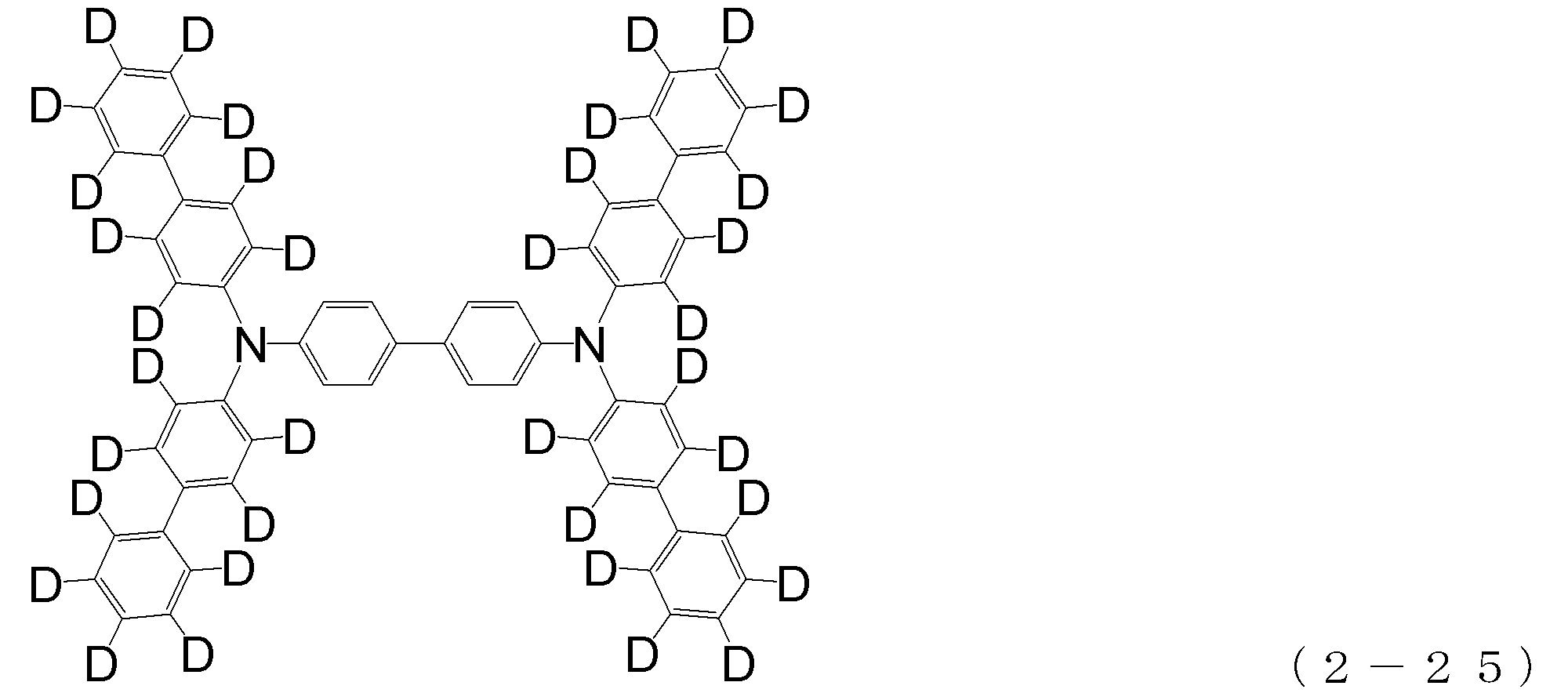
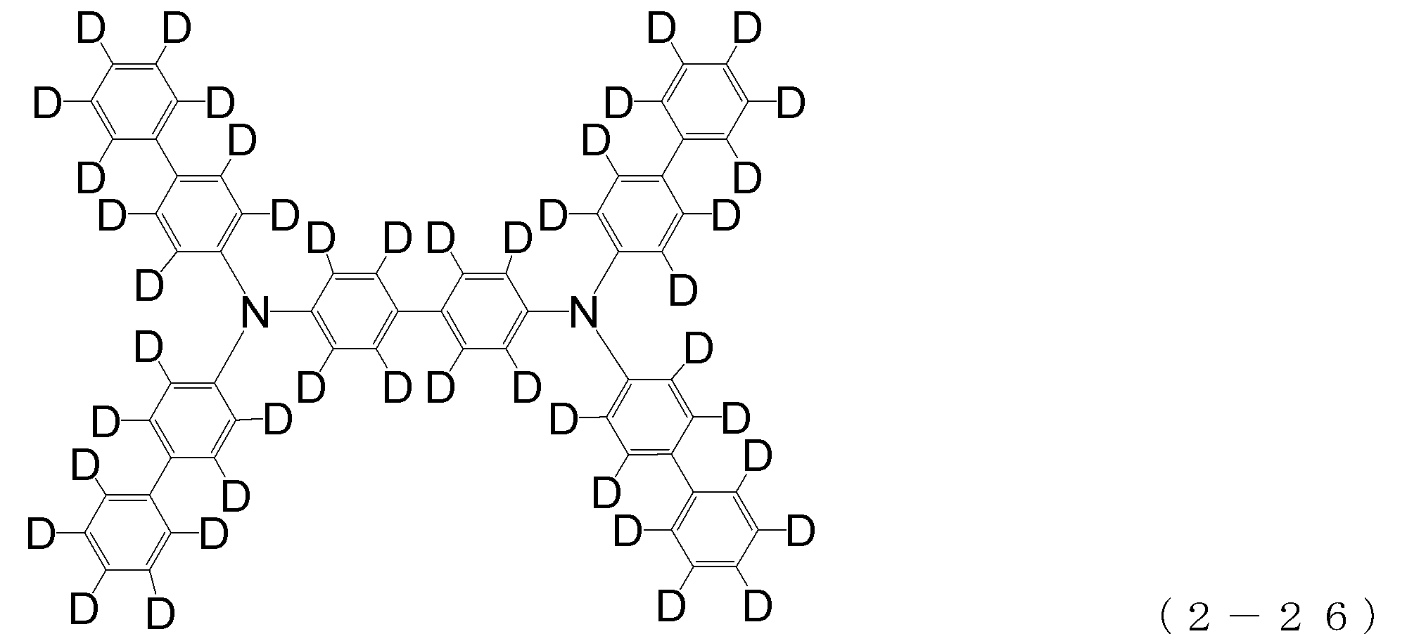


発光層は、従来公知の有機EL素子に使用されているものと同じであり、用いる材料の種類に応じて、蒸着法、スピンコート法、インクジェット法等の公知の方法によって形成される。
このときのホスト材料としては、4,4’-ジ(N-カルバゾリル)ビフェニル(CBP)、TCTA、mCPなどのカルバゾール誘導体などの正孔注入・輸送性のホスト材料を用いることができ、p-ビス(トリフェニルシリル)ベンゼン(UGH2)、2,2’,2’’-(1,3,5-フェニレン)-トリス(1-フェニル-1H-ベンズイミダゾール)(TPBI)などの電子輸送性のホスト材料も使用することができる。このようなホスト材料を使用することにより高性能の有機EL素子を作製することができる。
電子輸送層は、それ自体公知の電子輸送材料から形成されていてよく、Alq3等のキノリノール誘導体の金属錯体のほか、亜鉛、ベリリウム、アルミニウムなどの各種の金属錯体、トリアゾール誘導体、トリアジン誘導体、オキサジアゾール誘導体、チアジアゾール誘導体、カルボジイミド誘導体、キノキサリン誘導体、フェナントロリン誘導体、シロール誘導体などを用いることができる。
また、かかる電子輸送層は、単層構造に限定されるものではなく、上述した各種の化合物を用いて形成された層が積層された積層構造を有するものであってもよい。
本発明の有機EL素子の陰極としては、アルミニウムのような仕事関数の低い金属や、マグネシウム銀合金、マグネシウムインジウム合金、アルミニウムマグネシウム合金のような、より仕事関数の低い合金が電極材料として用いられる。
本発明の有機EL素子は、上述の基本構造を有している限り、必要に応じてその他の層を有していてもよい。例えば、陽極と正孔輸送層との間に正孔注入層を設けることができ、正孔輸送層と発光層との間には電子阻止層を設けることができる。また、発光層と電子輸送層との間に正孔阻止層を設けることができる。さらに、電子輸送と陰極との間には、電子注入層を設けることができる。これらの正孔注入層、電子阻止層、正孔阻止層及び電子注入層は、それ自体公知の材料から形成されていてよく、何れも用いる材料の種類に応じて、蒸着法、スピンコート法、インクジェット法等の公知の方法によって形成される。
陽極と正孔輸送層との間に形成される正孔注入層は、前述したアリールアミン化合物(X)により正孔注入層が形成されていることが好ましい。即ち、このアリールアミン化合物(X)は、正孔移動度が極めて大きいからである。
電子阻止層を形成するための材料としては、電子阻止性を有する種々の化合物を使用することができ、下記のカルバゾール誘導体が代表的である。
4,4’,4’’-トリ(N-カルバゾリル)トリフェニルアミン
(TCTA);
9,9-ビス[4-(カルバゾール-9-イル)フェニル]フルオレン;
1,3-ビス(カルバゾール-9-イル)ベンゼン(mCP);
2,2-ビス(4-カルバゾール-9-イルフェニル)アダマンタン
(Ad-Cz);
また、上記のカルバゾール誘導体以外にも、9-[4-(カルバゾール-9-イル)フェニル]-9-[4-(トリフェニルシリル)フェニル]-9H-フルオレンに代表されるトリフェニルシリル基を有しており且つトリアリールアミン骨格を分子中に有している化合物なども、電子阻止層形成用の材料として使用することができる。
正孔阻止層は、バソクプロイン(BCP)などのフェナントロリン誘導体、アルミニウム(III)ビス(2-メチル-8-キノリナート)-4-フェニルフェノレート(BAlq)などのキノリノール誘導体の金属錯体の他、各種の希土類錯体、トリアゾール誘導体、トリアジン誘導体、オキサジアゾール誘導体など、正孔阻止作用を有する化合物により形成される。
電子注入層は、フッ化リチウム、フッ化セシウムなどのアルカリ金属塩、フッ化マグネシウムなどのアルカリ土類金属塩、酸化アルミニウムなどの金属酸化物などを用いて形成することができる。
尚、以下の実施例において、2種の化合物の重量比は、それぞれの化合物を単独で用いて同条件で蒸着を行ったときの蒸着速度(成膜速度)から算出したものである。
下記の手順で、図1に示す構造の有機EL素子を作製した。即ち、この有機EL素子は、ガラス基板1上に透明陽極2(ITO電極)、正孔注入層3、正孔輸送層4、発光層5、電子輸送層6、電子注入層7、陰極(アルミニウム電極)8が順に蒸着により設けられた構造を有している。
続いて、下記化合物(1-1)を用いての蒸着により、透明陽極2を覆うように膜厚20nmの正孔注入層3を形成した。
この正孔注入層3の上に、正孔輸送層4として下記化合物(1-1)と下記化合物(2-1)とを、重量比が20:80となる蒸着速度で二元蒸着を行い、膜厚40nmとなるように形成した。
この正孔輸送層4の上に、発光層5として下記化合物(3)と下記化合物(4)とを、重量比が5:95となる蒸着速度で二元蒸着を行い、膜厚30nmとなるように形成した。
この発光層5の上に、電子輸送層6としてAlq3を膜厚30nmとなるように蒸着した。
この電子輸送層6の上に、電子注入層7としてフッ化リチウムを膜厚0.5nmとなるように蒸着した。
最後に、アルミニウムを150nm蒸着して陰極8を形成した。
作製した有機EL素子について、大気中、常温で特性測定を行なった。作製した有機EL素子に直流電圧を印加したときの発光特性の測定結果を表1にまとめて示した。
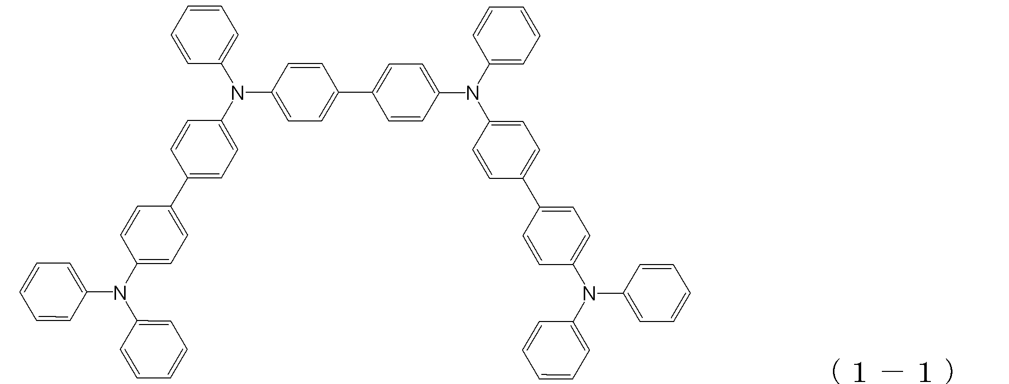
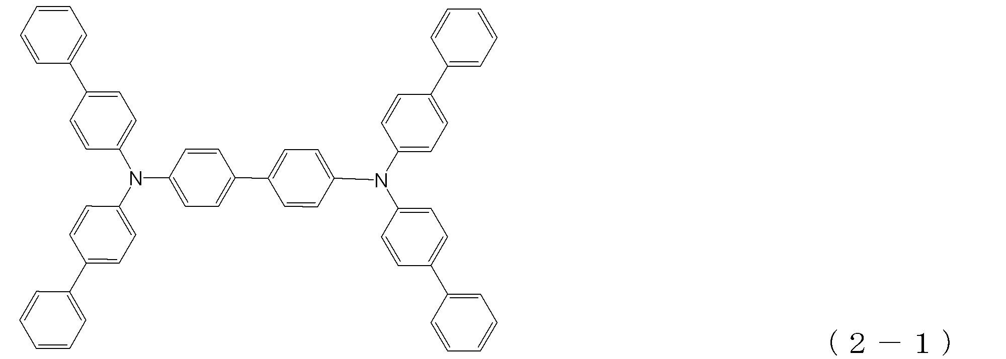

実施例1において、正孔輸送層4として前記化合物(1-1)と、前記化合物(2-1)とを、重量比が10:90となる蒸着速度で二元蒸着を行い、膜厚40nmとなるように形成した以外は、実施例1と同様の条件で有機EL素子を作製した。
作製した有機EL素子について、大気中、常温で特性測定を行なった。作製した有機EL素子に直流電圧を印加したときの発光特性の測定結果を表1にまとめて示した。
実施例1において、正孔輸送層4として前記化合物(1-1)と前記化合物(2-1)とを、重量比が40:60となる蒸着速度で二元蒸着を行い、膜厚40nmとなるように形成した以外は、実施例1と同様の条件で有機EL素子を作製した。
作製した有機EL素子について、大気中、常温で特性測定を行なった。作製した有機EL素子に直流電圧を印加したときの発光特性の測定結果を表1にまとめて示した。
実施例1において、正孔輸送層4として前記化合物(1-1)と前記化合物(2-1)とを、重量比が60:40となる蒸着速度で二元蒸着を行い、膜厚40nmとなるように形成した以外は、実施例1と同様の条件で有機EL素子を作製した。
作製した有機EL素子について、大気中、常温で特性測定を行なった。作製した有機EL素子に直流電圧を印加したときの発光特性の測定結果を表1にまとめて示した。
比較のために、実施例1において、正孔輸送層4として前記化合物(2-1)を膜厚40nmとなるように形成した以外は、実施例1と同様の条件で有機EL素子を作製した。
作製した有機EL素子について、大気中、常温で特性測定を行なった。作製した有機EL素子に直流電圧を印加したときの発光特性の測定結果を表1にまとめて示した。
比較のために、実施例1において、正孔輸送層4として前記構造式の化合物1-1を膜厚40nmとなるように形成した以外は、実施例1と同様の条件で有機EL素子を作製した。
作製した有機EL素子について、大気中、常温で特性測定を行なった。作製した有機EL素子に直流電圧を印加したときの発光特性の測定結果を表1にまとめて示した。
比較のために、実施例1において、正孔輸送層4として前記化合物(1-1)と前記化合物(2-1)とを、重量比が80:20となる蒸着速度で二元蒸着を行い、膜厚40nmとなるように形成した以外は、実施例1と同様の条件で有機EL素子を作製した。
作製した有機EL素子について、大気中、常温で特性測定を行なった。作製した有機EL素子に直流電圧を印加したときの発光特性の測定結果を表1にまとめて示した。
実施例1において、正孔輸送層4として下記化合物(1-16)と、下記化合物(2-22)とを、重量比が20:80となる蒸着速度で二元蒸着を行い、膜厚40nmとなるように形成した以外は、実施例1と同様の条件で有機EL素子を作製した。
作製した有機EL素子について、大気中、常温で特性測定を行なった。作製した有機EL素子に直流電圧を印加したときの発光特性の測定結果を表2にまとめて示した。
実施例5において、正孔輸送層4として前記化合物(1-16)と、前記化合物(2-22)とを、重量比が10:90となる蒸着速度で二元蒸着を行い、膜厚40nmとなるように形成した以外は、実施例5と同様の条件で有機EL素子を作製した。
作製した有機EL素子について、大気中、常温で特性測定を行なった。作製した有機EL素子に直流電圧を印加したときの発光特性の測定結果を表2にまとめて示した。
比較のために、実施例5において、正孔輸送層4として前記化合物(2-22)を膜厚40nmとなるように形成した以外は、実施例5と同様の条件で有機EL素子を作製した。
作製した有機EL素子について、大気中、常温で特性測定を行なった。作製した有機EL素子に直流電圧を印加したときの発光特性の測定結果を表2にまとめて示した。
比較のために、実施例5において、正孔輸送層4として前記化合物(1-16)を膜厚40nmとなるように形成した以外は、実施例5と同様の条件で有機EL素子を作製した。
作製した有機EL素子について、大気中、常温で特性測定を行なった。作製した有機EL素子に直流電圧を印加したときの発光特性の測定結果を表2にまとめて示した。
実施例1、比較例1および比較例2と同一の有機EL素子を用いて、素子寿命を測定した結果を表3にまとめて示した。素子寿命は、発光輝度1000cd/m2で発光させた時の電流量(W)を一定とした時の発光輝度について、初期輝度を100%とした時、輝度が95%まで減衰する時間を測定して求めた。

2 透明陽極
3 正孔注入層
4 正孔輸送層
5 発光層
6 電子輸送層
7 電子注入層
8 陰極
Claims (6)
- 陽極と陰極との間に、正孔輸送層、発光層及び電子輸送層が設けられている有機エレクトロルミネッセンス素子において、
前記正孔輸送層が、3個以上のトリフェニルアミン骨格が単結合或いは2価の炭化水素基で結合されている分子構造を有するアリールアミン化合物(X)と、2個のトリフェニルアミン骨格が単結合或いは2価の炭化水素基で結合されている分子構造を有するアリールアミン化合物(Y)とを含んでいる有機エレクトロルミネッセンス素子。 - 前記アリールアミン化合物(X)が、下記一般式(1)で表される請求項1に記載の有機エレクトロルミネッセンス素子。

r1~r12は、それぞれ、R1~R12の数を示すものであ
り、r1、r2、r5、r8、r11及びr12は、0~5の整
数を表し、
r3、r4、r6、r7、r9及びr10は、0~4の整数を
表し、
R1~R12は、それぞれ、重水素原子、フッ素原子、塩素原
子、シアノ基、トリフルオロメチル基、炭素原子数1ないし6の
無置換アルキル基、炭素原子数2ないし6の無置換もしくは置換
アルケニル基、無置換もしくは置換芳香族炭化水素基または無置
換もしくは置換芳香族複素環基であり、これらの基の中で同一の
ベンゼン環に結合しているもの同士は、互いに結合して環を形成
していてもよく、
A1~A3は、それぞれ、単結合或いは下記構造式(B)~
(F)で表される2価の炭化水素基を表す;





- 前記一般式(1)におけるR1~R12の少なくとも一つが、重水素原子もしくは重水素原子を含む基である請求項2に記載の有機エレクトロルミネッセンス素子。
- 前記アリールアミン化合物(Y)が、下記一般式(2)で表される請求項1に記載の有機エレクトロルミネッセンス素子。

r13~r18は、R13~R18の数を示すものであり、
r13、r14、r17及びr18は、0~5の整数であり、
r15及びr16は、0~4の整数を表し、
R13~R18は、それぞれ、重水素原子、フッ素原子、塩素
原子、シアノ基、トリフルオロメチル基、炭素原子数1ないし6
の無置換アルキル基、炭素原子数2ないし6の無置換もしくは置
換アルケニル基、無置換もしくは置換芳香族炭化水素基または無
置換もしくは置換芳香族複素環基であり、これらの基の中で同一
のベンゼン環に結合しているもの同士は、互いに結合して環を形
成していてもよく、
A4は、単結合または下記構造式(B)~(F)で表される2
価の炭化水素
基を示す;





- 前記一般式(2)におけるR13~R18の少なくとも一つが、重水素原子、もしくは重水素原子を含む基である請求項4に記載の有機エレクトロルミネッセンス素子。
- 前記アリールアミン化合物(X)とアリールアミン化合物(Y)とが、X:Y=1:9~6:4の重量比で前記正孔輸送層に含まれている請求項1に記載の有機エレクトロルミネッセンス素子。
Priority Applications (5)
| Application Number | Priority Date | Filing Date | Title |
|---|---|---|---|
| JP2013502295A JP5977227B2 (ja) | 2011-02-28 | 2012-02-24 | 有機エレクトロルミネッセンス素子 |
| US14/001,560 US9444055B2 (en) | 2011-02-28 | 2012-02-24 | Organic electroluminescent device |
| KR1020137022625A KR101947201B1 (ko) | 2011-02-28 | 2012-02-24 | 유기 일렉트로루미네선스 소자 |
| EP12752444.5A EP2682997A4 (en) | 2011-02-28 | 2012-02-24 | ORGANIC ELECTROLUMINESCENCE ELEMENT |
| CN2012800108674A CN103403909A (zh) | 2011-02-28 | 2012-02-24 | 有机电致发光器件 |
Applications Claiming Priority (2)
| Application Number | Priority Date | Filing Date | Title |
|---|---|---|---|
| JP2011-042169 | 2011-02-28 | ||
| JP2011042169 | 2011-02-28 |
Publications (1)
| Publication Number | Publication Date |
|---|---|
| WO2012117973A1 true WO2012117973A1 (ja) | 2012-09-07 |
Family
ID=46757910
Family Applications (1)
| Application Number | Title | Priority Date | Filing Date |
|---|---|---|---|
| PCT/JP2012/054605 Ceased WO2012117973A1 (ja) | 2011-02-28 | 2012-02-24 | 有機エレクトロルミネッセンス素子 |
Country Status (7)
| Country | Link |
|---|---|
| US (1) | US9444055B2 (ja) |
| EP (1) | EP2682997A4 (ja) |
| JP (1) | JP5977227B2 (ja) |
| KR (1) | KR101947201B1 (ja) |
| CN (1) | CN103403909A (ja) |
| TW (1) | TWI568710B (ja) |
| WO (1) | WO2012117973A1 (ja) |
Cited By (4)
| Publication number | Priority date | Publication date | Assignee | Title |
|---|---|---|---|---|
| WO2016088759A1 (ja) * | 2014-12-05 | 2016-06-09 | 保土谷化学工業株式会社 | 有機エレクトロルミネッセンス素子 |
| WO2017086357A1 (ja) | 2015-11-17 | 2017-05-26 | 保土谷化学工業株式会社 | 有機エレクトロルミネッセンス素子 |
| CN107431142A (zh) * | 2015-04-10 | 2017-12-01 | 保土谷化学工业株式会社 | 有机电致发光器件 |
| WO2018074529A1 (ja) | 2016-10-19 | 2018-04-26 | 保土谷化学工業株式会社 | インデノカルバゾール化合物および有機エレクトロルミネッセンス素子 |
Families Citing this family (7)
| Publication number | Priority date | Publication date | Assignee | Title |
|---|---|---|---|---|
| EP2704225B1 (en) | 2011-04-25 | 2019-02-06 | Hodogaya Chemical Co., Ltd. | Organic electroluminescent element |
| US9123897B2 (en) | 2011-10-14 | 2015-09-01 | Hodogaya Chemical Co., Ltd. | Benzotriazole derivatives and organic electroluminescent devices using the derivatives |
| US9502653B2 (en) | 2013-12-25 | 2016-11-22 | Ignis Innovation Inc. | Electrode contacts |
| EP3244463B1 (en) * | 2015-01-08 | 2020-07-22 | Hodogaya Chemical Co., Ltd. | Organic electroluminescent device |
| US11251373B2 (en) * | 2016-11-30 | 2022-02-15 | Hodogaya Chemical Co., Ltd. | High molecular weight compound containing substituted triarylamine structural unit |
| KR102668890B1 (ko) * | 2017-04-03 | 2024-05-27 | 듀폰스페셜티머터리얼스코리아 유한회사 | 유기 전계 발광 소자 |
| CN111470984B (zh) * | 2020-04-16 | 2022-12-13 | 苏州欧谱科显示科技有限公司 | 一种空穴传输材料及其制备方法和应用 |
Citations (15)
| Publication number | Priority date | Publication date | Assignee | Title |
|---|---|---|---|---|
| US4720432A (en) | 1987-02-11 | 1988-01-19 | Eastman Kodak Company | Electroluminescent device with organic luminescent medium |
| JPH06314594A (ja) | 1992-12-18 | 1994-11-08 | Ricoh Co Ltd | 複数のキャリヤー注入層を有する有機薄膜el素子 |
| JPH07126615A (ja) | 1993-11-01 | 1995-05-16 | Matsushita Electric Ind Co Ltd | 電界発光素子 |
| JPH0848656A (ja) | 1994-02-08 | 1996-02-20 | Tdk Corp | 有機el素子用化合物および有機el素子 |
| JPH08291115A (ja) | 1995-04-21 | 1996-11-05 | Bando Chem Ind Ltd | 新規なトリフェニルアミン化合物 |
| JPH11260559A (ja) * | 1998-03-11 | 1999-09-24 | Matsushita Electric Ind Co Ltd | 有機薄膜el素子およびその製造方法 |
| JP2001114735A (ja) * | 1999-10-08 | 2001-04-24 | Hodogaya Chem Co Ltd | 電子製品材料 |
| JP2001273978A (ja) * | 2001-02-23 | 2001-10-05 | Matsushita Electric Ind Co Ltd | 電界発光素子 |
| JP2002053533A (ja) * | 2000-08-11 | 2002-02-19 | Hodogaya Chem Co Ltd | アリールアミン化合物 |
| JP2005015419A (ja) * | 2003-06-27 | 2005-01-20 | Canon Inc | アミノアントリル誘導基置換化合物およびそれを使用した有機発光素子 |
| JP2005108804A (ja) | 2003-05-27 | 2005-04-21 | Denso Corp | 有機el素子およびその製造方法 |
| JP2009530371A (ja) * | 2006-03-23 | 2009-08-27 | エルジー・ケム・リミテッド | 新規なジアミン誘導体、その製造方法およびそれを用いた有機電気素子 |
| WO2009139475A1 (ja) * | 2008-05-16 | 2009-11-19 | 保土谷化学工業株式会社 | 有機エレクトロルミネッセンス素子 |
| WO2009151039A1 (ja) * | 2008-06-11 | 2009-12-17 | 保土谷化学工業株式会社 | 有機エレクトロルミネッセンス素子 |
| WO2011093056A1 (ja) * | 2010-01-26 | 2011-08-04 | 保土谷化学工業株式会社 | トリフェニルアミン構造を有する化合物および有機エレクトロルミネッセンス素子 |
Family Cites Families (6)
| Publication number | Priority date | Publication date | Assignee | Title |
|---|---|---|---|---|
| JPS529735A (en) | 1975-07-11 | 1977-01-25 | Hitachi Ltd | Pinion stopper device for starter |
| EP0650955B1 (en) | 1993-11-01 | 1998-08-19 | Hodogaya Chemical Co., Ltd. | Amine compound and electro-luminescence device comprising same |
| EP0666298A3 (en) | 1994-02-08 | 1995-11-15 | Tdk Corp | Organic electroluminescent element and compound used therein. |
| US6579630B2 (en) * | 2000-12-07 | 2003-06-17 | Canon Kabushiki Kaisha | Deuterated semiconducting organic compounds used for opto-electronic devices |
| US20060182994A1 (en) * | 2005-01-18 | 2006-08-17 | Yukinari Sakamoto | Anthracene derivative, organic electroluminescent device, and display unit |
| KR100739498B1 (ko) * | 2005-05-07 | 2007-07-19 | 주식회사 두산 | 중수소화된 신규 아릴아민 유도체, 그 제조 방법 및 이를이용한 유기 전계 발광 소자 |
-
2012
- 2012-02-24 KR KR1020137022625A patent/KR101947201B1/ko active Active
- 2012-02-24 US US14/001,560 patent/US9444055B2/en active Active
- 2012-02-24 JP JP2013502295A patent/JP5977227B2/ja active Active
- 2012-02-24 EP EP12752444.5A patent/EP2682997A4/en not_active Withdrawn
- 2012-02-24 CN CN2012800108674A patent/CN103403909A/zh active Pending
- 2012-02-24 WO PCT/JP2012/054605 patent/WO2012117973A1/ja not_active Ceased
- 2012-02-29 TW TW101106520A patent/TWI568710B/zh active
Patent Citations (17)
| Publication number | Priority date | Publication date | Assignee | Title |
|---|---|---|---|---|
| US4720432A (en) | 1987-02-11 | 1988-01-19 | Eastman Kodak Company | Electroluminescent device with organic luminescent medium |
| JPH06314594A (ja) | 1992-12-18 | 1994-11-08 | Ricoh Co Ltd | 複数のキャリヤー注入層を有する有機薄膜el素子 |
| JPH07126615A (ja) | 1993-11-01 | 1995-05-16 | Matsushita Electric Ind Co Ltd | 電界発光素子 |
| JP3194657B2 (ja) | 1993-11-01 | 2001-07-30 | 松下電器産業株式会社 | 電界発光素子 |
| JPH0848656A (ja) | 1994-02-08 | 1996-02-20 | Tdk Corp | 有機el素子用化合物および有機el素子 |
| JPH08291115A (ja) | 1995-04-21 | 1996-11-05 | Bando Chem Ind Ltd | 新規なトリフェニルアミン化合物 |
| JPH11260559A (ja) * | 1998-03-11 | 1999-09-24 | Matsushita Electric Ind Co Ltd | 有機薄膜el素子およびその製造方法 |
| JP2001114735A (ja) * | 1999-10-08 | 2001-04-24 | Hodogaya Chem Co Ltd | 電子製品材料 |
| JP2002053533A (ja) * | 2000-08-11 | 2002-02-19 | Hodogaya Chem Co Ltd | アリールアミン化合物 |
| JP2001273978A (ja) * | 2001-02-23 | 2001-10-05 | Matsushita Electric Ind Co Ltd | 電界発光素子 |
| JP3529735B2 (ja) | 2001-02-23 | 2004-05-24 | 松下電器産業株式会社 | 電界発光素子 |
| JP2005108804A (ja) | 2003-05-27 | 2005-04-21 | Denso Corp | 有機el素子およびその製造方法 |
| JP2005015419A (ja) * | 2003-06-27 | 2005-01-20 | Canon Inc | アミノアントリル誘導基置換化合物およびそれを使用した有機発光素子 |
| JP2009530371A (ja) * | 2006-03-23 | 2009-08-27 | エルジー・ケム・リミテッド | 新規なジアミン誘導体、その製造方法およびそれを用いた有機電気素子 |
| WO2009139475A1 (ja) * | 2008-05-16 | 2009-11-19 | 保土谷化学工業株式会社 | 有機エレクトロルミネッセンス素子 |
| WO2009151039A1 (ja) * | 2008-06-11 | 2009-12-17 | 保土谷化学工業株式会社 | 有機エレクトロルミネッセンス素子 |
| WO2011093056A1 (ja) * | 2010-01-26 | 2011-08-04 | 保土谷化学工業株式会社 | トリフェニルアミン構造を有する化合物および有機エレクトロルミネッセンス素子 |
Non-Patent Citations (1)
| Title |
|---|
| See also references of EP2682997A4 |
Cited By (10)
| Publication number | Priority date | Publication date | Assignee | Title |
|---|---|---|---|---|
| WO2016088759A1 (ja) * | 2014-12-05 | 2016-06-09 | 保土谷化学工業株式会社 | 有機エレクトロルミネッセンス素子 |
| CN107004773A (zh) * | 2014-12-05 | 2017-08-01 | 保土谷化学工业株式会社 | 有机电致发光器件 |
| JPWO2016088759A1 (ja) * | 2014-12-05 | 2017-09-21 | 保土谷化学工業株式会社 | 有機エレクトロルミネッセンス素子 |
| US11158811B2 (en) | 2014-12-05 | 2021-10-26 | Hodogaya Chemical Co., Ltd. | Organic electroluminescent device |
| CN107431142A (zh) * | 2015-04-10 | 2017-12-01 | 保土谷化学工业株式会社 | 有机电致发光器件 |
| CN107431142B (zh) * | 2015-04-10 | 2021-02-02 | 保土谷化学工业株式会社 | 有机电致发光器件 |
| WO2017086357A1 (ja) | 2015-11-17 | 2017-05-26 | 保土谷化学工業株式会社 | 有機エレクトロルミネッセンス素子 |
| WO2018074529A1 (ja) | 2016-10-19 | 2018-04-26 | 保土谷化学工業株式会社 | インデノカルバゾール化合物および有機エレクトロルミネッセンス素子 |
| KR20190065407A (ko) | 2016-10-19 | 2019-06-11 | 호도가야 가가쿠 고교 가부시키가이샤 | 인데노카르바졸 화합물 및 유기 일렉트로루미네선스 소자 |
| US11925114B2 (en) | 2016-10-19 | 2024-03-05 | Hodogaya Chemical Co., Ltd. | Indenocarbazole compound and organic electroluminescence device |
Also Published As
| Publication number | Publication date |
|---|---|
| JPWO2012117973A1 (ja) | 2014-07-07 |
| EP2682997A1 (en) | 2014-01-08 |
| TW201242929A (en) | 2012-11-01 |
| US9444055B2 (en) | 2016-09-13 |
| CN103403909A (zh) | 2013-11-20 |
| EP2682997A4 (en) | 2014-09-10 |
| JP5977227B2 (ja) | 2016-08-24 |
| US20130328040A1 (en) | 2013-12-12 |
| TWI568710B (zh) | 2017-02-01 |
| KR20140020260A (ko) | 2014-02-18 |
| KR101947201B1 (ko) | 2019-02-12 |
Similar Documents
| Publication | Publication Date | Title |
|---|---|---|
| JP5977227B2 (ja) | 有機エレクトロルミネッセンス素子 | |
| US10615350B2 (en) | Organic light-emitting element and display apparatus | |
| KR101745109B1 (ko) | 유기 발광 소자 | |
| KR101544237B1 (ko) | 유기 전계 발광 소자 | |
| KR101993015B1 (ko) | 유기 일렉트로루미네선스 소자 | |
| TW201341360A (zh) | 發光元件 | |
| JP2023068108A (ja) | 有機電界発光素子 | |
| CN102576813A (zh) | 有机电致发光器件 | |
| KR20160064948A (ko) | 모노아민 유도체 및 이를 포함하는 유기 일렉트로루미네센스 소자 | |
| KR20160002675A (ko) | 화합물, 유기 전기발광 소자용 재료, 유기 전기발광 소자 및 전자 기기 | |
| US11925107B2 (en) | Organic electroluminescent device | |
| KR20210036253A (ko) | 화합물 및 이를 포함하는 유기 발광 소자 | |
| KR20160149975A (ko) | 유기 전계 발광 소자용 재료 및 이를 포함하는 유기 전계 발광 소자 | |
| JP2016108290A (ja) | アミン誘導体、および有機エレクトロルミネッセンス素子 | |
| US20120119196A1 (en) | Organic electroluminescent element | |
| WO2012098849A1 (ja) | 置換されたビピリジル基とピリドインドール環構造を有する化合物および有機エレクトロルミネッセンス素子 | |
| TW201920602A (zh) | 有機電致發光元件 | |
| EP3890042A1 (en) | Organic electroluminescence element | |
| WO2023136295A1 (ja) | ピリミジン化合物および有機エレクトロルミネッセンス素子 | |
| JP2016108292A (ja) | モノアミン誘導体、および有機エレクトロルミネッセンス素子 | |
| JP6580321B2 (ja) | モノアミン誘導体、および有機エレクトロルミネッセンス素子 | |
| EP4401529A1 (en) | Organic electroluminescent element | |
| JP2019034904A (ja) | 芳香族炭化水素基と2つのフタルイミド基を有する化合物および有機エレクトロルミネッセンス素子 | |
| WO2024208890A1 (en) | Organic electroluminescent device comprising a organic matrix compound and organic electron transport compound of formula (i), and display device comprising the organic electroluminescent device | |
| WO2019039402A1 (ja) | インデノベンゾアゾール環構造を有する化合物および有機エレクトロルミネッセンス素子 |
Legal Events
| Date | Code | Title | Description |
|---|---|---|---|
| 121 | Ep: the epo has been informed by wipo that ep was designated in this application |
Ref document number: 12752444 Country of ref document: EP Kind code of ref document: A1 |
|
| ENP | Entry into the national phase |
Ref document number: 2013502295 Country of ref document: JP Kind code of ref document: A |
|
| WWE | Wipo information: entry into national phase |
Ref document number: 14001560 Country of ref document: US |
|
| ENP | Entry into the national phase |
Ref document number: 20137022625 Country of ref document: KR Kind code of ref document: A |
|
| NENP | Non-entry into the national phase |
Ref country code: DE |
|
| REEP | Request for entry into the european phase |
Ref document number: 2012752444 Country of ref document: EP |
|
| WWE | Wipo information: entry into national phase |
Ref document number: 2012752444 Country of ref document: EP |