WO2012121221A1 - Procédés de fabrication de matrice de formation, de lentille mince et de lentille optique - Google Patents
Procédés de fabrication de matrice de formation, de lentille mince et de lentille optique Download PDFInfo
- Publication number
- WO2012121221A1 WO2012121221A1 PCT/JP2012/055589 JP2012055589W WO2012121221A1 WO 2012121221 A1 WO2012121221 A1 WO 2012121221A1 JP 2012055589 W JP2012055589 W JP 2012055589W WO 2012121221 A1 WO2012121221 A1 WO 2012121221A1
- Authority
- WO
- WIPO (PCT)
- Prior art keywords
- mold
- resin
- substrate
- master
- sub
- Prior art date
- Legal status (The legal status is an assumption and is not a legal conclusion. Google has not performed a legal analysis and makes no representation as to the accuracy of the status listed.)
- Ceased
Links
Images




Classifications
-
- B—PERFORMING OPERATIONS; TRANSPORTING
- B29—WORKING OF PLASTICS; WORKING OF SUBSTANCES IN A PLASTIC STATE IN GENERAL
- B29D—PRODUCING PARTICULAR ARTICLES FROM PLASTICS OR FROM SUBSTANCES IN A PLASTIC STATE
- B29D11/00—Producing optical elements, e.g. lenses or prisms
- B29D11/00009—Production of simple or compound lenses
- B29D11/00317—Production of lenses with markings or patterns
-
- B—PERFORMING OPERATIONS; TRANSPORTING
- B29—WORKING OF PLASTICS; WORKING OF SUBSTANCES IN A PLASTIC STATE IN GENERAL
- B29C—SHAPING OR JOINING OF PLASTICS; SHAPING OF MATERIAL IN A PLASTIC STATE, NOT OTHERWISE PROVIDED FOR; AFTER-TREATMENT OF THE SHAPED PRODUCTS, e.g. REPAIRING
- B29C33/00—Moulds or cores; Details thereof or accessories therefor
- B29C33/38—Moulds or cores; Details thereof or accessories therefor characterised by the material or the manufacturing process
- B29C33/3842—Manufacturing moulds, e.g. shaping the mould surface by machining
- B29C33/3857—Manufacturing moulds, e.g. shaping the mould surface by machining by making impressions of one or more parts of models, e.g. shaped articles and including possible subsequent assembly of the parts
-
- B—PERFORMING OPERATIONS; TRANSPORTING
- B29—WORKING OF PLASTICS; WORKING OF SUBSTANCES IN A PLASTIC STATE IN GENERAL
- B29C—SHAPING OR JOINING OF PLASTICS; SHAPING OF MATERIAL IN A PLASTIC STATE, NOT OTHERWISE PROVIDED FOR; AFTER-TREATMENT OF THE SHAPED PRODUCTS, e.g. REPAIRING
- B29C35/00—Heating, cooling or curing, e.g. crosslinking or vulcanising; Apparatus therefor
- B29C35/02—Heating or curing, e.g. crosslinking or vulcanizing during moulding, e.g. in a mould
- B29C35/08—Heating or curing, e.g. crosslinking or vulcanizing during moulding, e.g. in a mould by wave energy or particle radiation
- B29C35/0888—Heating or curing, e.g. crosslinking or vulcanizing during moulding, e.g. in a mould by wave energy or particle radiation using transparant moulds
-
- B—PERFORMING OPERATIONS; TRANSPORTING
- B29—WORKING OF PLASTICS; WORKING OF SUBSTANCES IN A PLASTIC STATE IN GENERAL
- B29C—SHAPING OR JOINING OF PLASTICS; SHAPING OF MATERIAL IN A PLASTIC STATE, NOT OTHERWISE PROVIDED FOR; AFTER-TREATMENT OF THE SHAPED PRODUCTS, e.g. REPAIRING
- B29C43/00—Compression moulding, i.e. applying external pressure to flow the moulding material; Apparatus therefor
- B29C43/02—Compression moulding, i.e. applying external pressure to flow the moulding material; Apparatus therefor of articles of definite length, i.e. discrete articles
- B29C43/021—Compression moulding, i.e. applying external pressure to flow the moulding material; Apparatus therefor of articles of definite length, i.e. discrete articles characterised by the shape of the surface
-
- B—PERFORMING OPERATIONS; TRANSPORTING
- B29—WORKING OF PLASTICS; WORKING OF SUBSTANCES IN A PLASTIC STATE IN GENERAL
- B29C—SHAPING OR JOINING OF PLASTICS; SHAPING OF MATERIAL IN A PLASTIC STATE, NOT OTHERWISE PROVIDED FOR; AFTER-TREATMENT OF THE SHAPED PRODUCTS, e.g. REPAIRING
- B29C43/00—Compression moulding, i.e. applying external pressure to flow the moulding material; Apparatus therefor
- B29C43/32—Component parts, details or accessories; Auxiliary operations
- B29C43/36—Moulds for making articles of definite length, i.e. discrete articles
-
- B—PERFORMING OPERATIONS; TRANSPORTING
- B29—WORKING OF PLASTICS; WORKING OF SUBSTANCES IN A PLASTIC STATE IN GENERAL
- B29D—PRODUCING PARTICULAR ARTICLES FROM PLASTICS OR FROM SUBSTANCES IN A PLASTIC STATE
- B29D11/00—Producing optical elements, e.g. lenses or prisms
- B29D11/00009—Production of simple or compound lenses
- B29D11/00278—Lenticular sheets
- B29D11/00307—Producing lens wafers
-
- B—PERFORMING OPERATIONS; TRANSPORTING
- B29—WORKING OF PLASTICS; WORKING OF SUBSTANCES IN A PLASTIC STATE IN GENERAL
- B29D—PRODUCING PARTICULAR ARTICLES FROM PLASTICS OR FROM SUBSTANCES IN A PLASTIC STATE
- B29D11/00—Producing optical elements, e.g. lenses or prisms
- B29D11/00009—Production of simple or compound lenses
- B29D11/0048—Moulds for lenses
-
- G—PHYSICS
- G02—OPTICS
- G02B—OPTICAL ELEMENTS, SYSTEMS OR APPARATUS
- G02B3/00—Simple or compound lenses
- G02B3/0006—Arrays
- G02B3/0012—Arrays characterised by the manufacturing method
- G02B3/0031—Replication or moulding, e.g. hot embossing, UV-casting, injection moulding
-
- B—PERFORMING OPERATIONS; TRANSPORTING
- B29—WORKING OF PLASTICS; WORKING OF SUBSTANCES IN A PLASTIC STATE IN GENERAL
- B29C—SHAPING OR JOINING OF PLASTICS; SHAPING OF MATERIAL IN A PLASTIC STATE, NOT OTHERWISE PROVIDED FOR; AFTER-TREATMENT OF THE SHAPED PRODUCTS, e.g. REPAIRING
- B29C35/00—Heating, cooling or curing, e.g. crosslinking or vulcanising; Apparatus therefor
- B29C35/02—Heating or curing, e.g. crosslinking or vulcanizing during moulding, e.g. in a mould
- B29C35/08—Heating or curing, e.g. crosslinking or vulcanizing during moulding, e.g. in a mould by wave energy or particle radiation
- B29C35/0805—Heating or curing, e.g. crosslinking or vulcanizing during moulding, e.g. in a mould by wave energy or particle radiation using electromagnetic radiation
- B29C2035/0827—Heating or curing, e.g. crosslinking or vulcanizing during moulding, e.g. in a mould by wave energy or particle radiation using electromagnetic radiation using UV radiation
-
- B—PERFORMING OPERATIONS; TRANSPORTING
- B29—WORKING OF PLASTICS; WORKING OF SUBSTANCES IN A PLASTIC STATE IN GENERAL
- B29L—INDEXING SCHEME ASSOCIATED WITH SUBCLASS B29C, RELATING TO PARTICULAR ARTICLES
- B29L2011/00—Optical elements, e.g. lenses, prisms
- B29L2011/0016—Lenses
Definitions
- the present invention relates to a mold used for manufacturing a wafer lens having a plurality of optical lenses, a wafer lens using the mold, and a method for manufacturing the optical lens, and in particular, a resin shape transfer layer by transfer onto a substrate.
- the present invention relates to a method for manufacturing a mold, a wafer lens, and an optical lens obtained by forming the lens.
- a first master replication tool made of resin or the like is produced by repeatedly transferring a small master mold, and then a plurality of sub master molds are created from the first generation replication tool.
- manufacturing a plurality of second generation replication tools provided with a large number of micro optical elements from a sub-master type is known (see Patent Document 1).
- the wafer-shaped first generation replication tool obtained by this method is a mold for producing the next molded product, and is formed by forming a resin shape transfer layer on a substrate.
- the use of small optical lenses is increasing, and the optical lens is required to accurately realize the intended lens shape so that the desired optical performance can be exhibited.
- a plurality of optical lenses may be stacked in order to improve optical performance. From these viewpoints, it is required not to make the resin layer of the wafer lens too thick. If the resin layer of the wafer lens is too thick, the desired optical performance may not be obtained, or the wafer lens may be warped or deformed due to increased stress of the resin layer. In addition, when the optical lenses are stacked, the overall size may increase. Furthermore, there is a problem that the material cost increases and the curing time increases.
- the present invention has been made in view of the above-described background art, and a mold having an intended shape can be obtained by reducing the mold release resistance, and an optical lens that exhibits the desired optical performance is formed. It aims at providing the manufacturing method of the shaping
- Another object of the present invention is to provide a highly accurate wafer lens and optical lens manufacturing method using a mold obtained by the above manufacturing method.
- a plurality of master molds having a first mold surface formed with a shape corresponding to the optical lens are repeatedly used on the first substrate.
- a method of manufacturing a molding die for obtaining a molding die having a plurality of resin replica portions by molding a resin replica (replica) portion, wherein the arrangement position on one side of a checkered pattern (checks) of the first substrate A first step of forming a plurality of first-stage resin replica portions among the plurality of resin replica portions by interposing a resin material between the master mold and the first substrate, and a checkered pattern remaining in the first substrate And a second step of forming a plurality of second-stage resin replica portions among the plurality of resin replica portions by interposing a resin material between the master mold and the first substrate, Each first tree formed Each second-stage resin replica portion is formed in the second step so that the end portion of each second-stage resin replica portion overlaps the end portion of the oil replica portion.
- the above manufacturing method first the first phase resin replica portion isolated from the periphery is formed, and then the second phase resin replica portion surrounded by the periphery is formed. At this time, since the end of each second-stage resin replica portion overlaps with the end of each first-stage resin replica portion, occurrence of an under shape or an overhang shape can be prevented. As a result, in the molding process using the present mold, it is possible to prevent the occurrence of an unintended shape and reduce or eliminate the mold release resistance. This reduces the formation of local release resistance distribution during molding of the wafer lens and suppresses local deformation, thereby eliminating the shape difference between many lenses in the wafer lens and improving molding accuracy. It is possible to provide an accurate and stable lens.
- the first molding surface has a plurality of first optical transfer surfaces arranged two-dimensionally.
- the first molding surface has a plurality of first optical transfer surfaces, and the number of lenses in the first substrate can be increased.
- the number of times of transfer that is, stamping by the master mold can be reduced, the working time for manufacturing the mold is shortened.
- each first-stage resin replica portion is molded with an amount of resin that can cover the width.
- the master mold interval is filled with the resin in the range as described above, so that in the second step, the reproducibility of the folded state of the outer edge of the second phase resin replica portion with respect to the outer edge of the first phase resin replica portion is achieved. Get better.
- a plurality of resin replica portions are molded on the first substrate by repeatedly using a master mold having a first molding surface formed with a shape corresponding to the optical lens.
- a first step of forming a plurality of first-stage resin replica portions among the plurality of resin replica portions with the interposition of the first mold and the remaining pattern of the checkerboard pattern between the master mold and the first substrate A second step of forming a plurality of second-stage resin replica portions among a plurality of resin replica portions with a resin material interposed therebetween, and a resin amount for forming each first-stage resin replica portion in the first step
- the second step Definitive larger than the amount of resin for forming the respective second phase resin replica unit.
- the first phase resin replica portion isolated from the periphery is formed, and then the second phase resin replica portion surrounded by the periphery is formed.
- the resin amount for forming each first-stage resin replica portion in the first step is larger than the resin amount for forming each second-phase resin replica portion in the second step, the first phase The resin is folded at the boundary between the resin replica portion and the second-stage resin replica portion, and the occurrence of an under shape or an overhang shape can be prevented.
- the molding process using the present mold it is possible to prevent the occurrence of an unintended shape and reduce or eliminate the mold release resistance. This reduces the formation of local release resistance distribution during molding of the wafer lens and suppresses local deformation, thereby eliminating the shape difference between many lenses in the wafer lens and improving molding accuracy. It is possible to provide an accurate and stable lens.
- the ratio of the resin amount in the first step to the resin amount in the second step (that is, the former / latter value) is 1.05 or more and 2.00 or less.
- the outer edge of the second-stage resin replica part is appropriately folded over the outer edge of the first-stage resin replica part.
- the connection part which connects between adjacent resin replica parts can be made into neither a protrusion shape nor an under shape.
- the master mold has a prismatic tip portion chamfered at a corner. In this case, it is possible to prevent a thick connecting portion from being formed outside the diagonal corner portion of the resin replica portion.
- the tip of the master mold has a flat surface chamfered at a corner, and the horizontal width of the flat surface is the larger of the widths of two wall surfaces adjacent to the flat surface. Of 1/20 or more and 1/3 or less. In this case, it is possible to prevent a thick connecting portion from being formed outside the diagonal corner portion of the resin replica portion without reducing the number of lenses taken from the wafer lens.
- the second-stage resin replica part is molded.
- the first-stage resin replica part and the second-stage resin replica part can be formed in parallel.
- the first substrate has a recessed portion having a size larger than the first molding surface and closed inside at a molding position corresponding to the resin replica portion, An annular step is formed around the first molding surface.
- a space where the resin material can spread can be formed between the step and the periphery of the recess.
- the first step and the second step fill and cure the first resin material between the first molding surface and the molding position on the first substrate, By releasing the mold, the transfer process for obtaining the resin replica portion to which the first molding surface has been transferred, and the transfer process are repeatedly performed while changing the relative position of the master mold and the first substrate.
- a molding die having the first shape transfer layer obtained by the above-described molding die manufacturing method is a first molding die, and the first molding die and the molding die are used.
- a second mold having a second shape transfer layer is obtained by filling the second resin material between the second substrate, curing the second resin material, and releasing the first mold. obtain.
- the second mold is a batch transfer mold for forming a wafer lens or the like.
- a third resin material is filled between the mold obtained by the above-described mold manufacturing method and the third substrate, and the third resin material is cured. Then, by releasing the mold, a wafer lens having a plurality of lens elements formed on the surface of the third substrate is obtained.
- a wafer lens or the like in which a plurality of lens elements are provided on one side of the third substrate can be obtained by duplication using transfer of the second mold or the like.
- a fourth resin material is provided between the mold obtained by the method for producing a mold and the back surface of the wafer lens obtained by the method for producing a wafer lens. Is satisfied, the fourth resin material is cured, and the mold is released to obtain a wafer lens having a plurality of lens elements formed on the back surface of the third substrate.
- a wafer lens or the like provided with a plurality of lens elements on both sides of the third substrate can be obtained by duplication using transfer of the second mold or the like.
- the method for manufacturing an optical lens according to the present invention includes a step of cutting and dividing the wafer lens obtained by the above-described method for manufacturing a wafer lens. In this case, a large number of high-performance optical lenses separated from the lens substrate can be obtained collectively.
- FIG. 3A is a perspective view illustrating a master mold used for manufacturing a wafer lens
- FIG. 3B is a plan view of the master mold
- FIG. 3C is a sub-master mold to be manufactured by the master mold.
- 4A is a perspective view illustrating a part of the master mold
- FIG. 4B is a perspective view illustrating a part of the sub master mold.
- FIG. 4C illustrates a part of the sub master model.
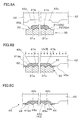
- FIG. 6A to 6C are views for explaining a wafer lens manufacturing process.
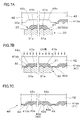
- 7A to 7C are diagrams for explaining the manufacturing process of the wafer lens.
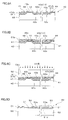
- 8A to 8D are views for explaining a wafer lens manufacturing process.
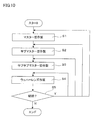
- 9A to 9C are views for explaining a manufacturing process of the wafer lens. It is a flowchart which illustrates the manufacturing process of a wafer lens notionally.
- 11A and 11B are diagrams for explaining the order of forming the resin layer portions on the sub-master substrate.
- FIG. 13A and 13B are views for explaining the side cross-sectional shape of the connecting portion that connects the first and second resin layer portions.
- 14A and 14B are views for explaining the order in which resin layer portions are formed on the sub-master substrate in the manufacturing method according to the second embodiment.
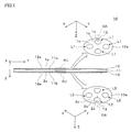
- the wafer lens 10 has a disk-like outer shape, and has a substrate 11, a first lens resin layer 12, and a second lens resin layer 13. .
- the wafer lens 10 may be referred to as a lens substrate.
- the surfaces of the first lens resin layer 12 and the second lens resin layer 13 are partially enlarged and shown as a perspective view.
- the substrate 11 is a circular flat plate (third substrate described later) embedded in the center of the wafer lens 10, and is formed of light transmissive glass.
- the outer diameter of the substrate 11 is substantially the same as the outer diameter of the first and second lens resin layers 12 and 13.
- the thickness of the substrate 11 is basically determined by optical specifications, but is at least a thickness that does not cause damage when the molded product is released to obtain the wafer lens 10.
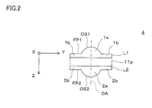
- the first lens resin layer 12 has optical transparency and is formed on one surface 11 a of the substrate 11. As shown in the partially enlarged perspective view, the first lens resin layer 12 is formed by two-dimensionally arranging a large number of first lens elements L1 each including a first lens body 1a and a first flange portion 1b in an XY plane. Are arranged. These first lens elements L1 are integrally formed through a connecting portion 1c. The combined surface of each first lens element L1 and the connecting portion 1c is a first transfer surface 12a that is collectively molded by transfer. As shown in FIG. 2, the first lens body 1a is, for example, a convex aspherical or spherical lens part, and has a first optical surface OS1.
- the surrounding first flange portion 1b has a flat first flange surface FP1 extending around the first optical surface OS1, and the outer periphery of the first flange surface FP1 is also the surface of the connecting portion 1c.
- the first flange surface FP1 is disposed in parallel to the XY plane perpendicular to the optical axis OA.
- the first lens resin layer 12 is divided into a number of array units AU derived from the manufacturing process, and these array units AU are rectangular, although detailed illustration is omitted. Are arranged on the substrate 11 in a matrix or a lattice.
- Each array unit AU has a surface shape that is an inversion of an end face 30b (see FIG. 3A) of a master mold 30 to be described later, and has a large number of first lens bodies 1a arranged in a matrix at equal intervals. is doing.
- the first lens resin layer 12 is made of, for example, a photocurable resin.
- the photocurable resin is composed of a polymerizable composition such as a polymerizable monomer as a main component, a photopolymerization initiator for initiating polymerization and curing of the polymerizable composition, and various additives used as necessary. It is obtained by curing a photocurable resin material containing Such a photocurable resin material has fluidity in a state before curing.
- the photocurable resin include an epoxy resin, an acrylic resin, an allyl ester resin, and a vinyl resin.
- the epoxy resin can be obtained by reactive curing of the polymerizable composition by cationic polymerization of a photopolymerization initiator.
- the acrylic resin, allyl ester resin, and vinyl resin can be obtained by reaction-curing the polymerizable composition by radical polymerization of a photopolymerization initiator.
- the second lens resin layer 13 is light-transmitting and is formed on the other surface 11b of the substrate 11.
- the second lens resin layer 13 is formed by two-dimensionally arranging a large number of second lens elements L2 each including the second lens body 2a and the second flange portion 2b in the XY plane. Are arranged. These second lens elements L2 are integrally molded via the connecting portion 2c. The combined surface of each second lens element L2 and the connecting portion 2c is a second transferred surface 13a that is collectively molded by transfer.
- the second lens body 2a is, for example, a convex aspherical or spherical lens portion, and has a second optical surface OS2.
- the surrounding second flange portion 2b has a flat second flange surface FP2 extending around the second optical surface OS2.
- the outer periphery of the second flange surface FP2 is also the surface of the connecting portion 2c.
- the second flange surface FP2 is disposed in parallel to the XY plane perpendicular to the optical axis OA.
- the second lens resin layer 13 is also divided into a large number of array units AU derived from the manufacturing process. These array units AU have a rectangular outline and are arranged in a matrix or lattice on the substrate 11. Is arranged.
- the photocurable resin used for the second lens resin layer 13 is the same photocurable resin as that used for the first lens resin layer 12. However, both lens resin layers 12 and 13 do not need to be formed of the same photocurable resin, and can be formed of different photocurable resins.
- One of the first lens resin layer 12 and the second lens resin layer 13 can be omitted. That is, the lens resin layer may be provided only on one surface 11a or the other surface 11b of the substrate 11.
- the optical lens 4 is a compound lens having a square shape in plan view obtained by dicing the wafer lens 10 by dicing the wafer lens 10 at the positions of the connecting portions 1c and 2c.
- the wafer lens 10 in FIG. 1 is manufactured by performing three-stage transfer using the master mold 30 shown in FIG. 3A as a master.
- the structure of the master mold 30 and a mold having a resin shape transfer surface obtained therefrom will be described.
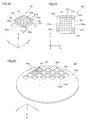
- the master die 30 is a rectangular parallelepiped block member, and at its end 30a, a substantially rectangular end surface 30b and an annular step 32 provided around the end surface 30b. And have.
- the end surface 30b is a first molding surface 31 for forming the second molding surface 43 of the sub-master mold 40 in FIG. 4B.
- the end 30a is chamfered at the four corners of the side surface. That is, the end 30a has four small flat surfaces 30c corresponding to chamfering. Each flat surface 30c extends perpendicularly from the four corners of the end surface 30b to the end surface 30b, and is inclined by 45 ° with respect to the X axis and the Y axis.
- the horizontal width of the flat surface 30c is about one side of the end surface 30b parallel to the X-axis and Y-axis, that is, the larger of the widths of two wall surfaces adjacent to the flat surface 30c (in the specific example, both are equal and both are 17 mm).
- the ratio is about 1/20 times or more and about 1/3 times or less, more preferably about 1/15 times or more and about 1/5 times or less.
- the master die 30 is repeatedly used for the production of the sub master die 40.
- the master die 30 is formed in a shallow rectangular recess 42c uniformly formed in a matrix or lattice arrangement on the sub master substrate 42 in FIG. 3C.
- Units (resin layer portions 41da and 41db in FIG. 8A to be described later) arranged separately on the sub-master substrate 42 are collected by step-and-repeat transfer that repeats transfer while moving two-dimensionally so as to face each other.
- the sub master resin layer (first shape transfer layer) 41 can be formed.
- the first molding surface 31 of the master mold 30 has an outer circumference that is slightly smaller than the recess 42c, and partially reverses the first transfer surface 12a of the first lens resin layer 12 of the wafer lens 10 that is finally obtained.
- the first molding surface 31 includes a first optical transfer surface 31a for forming the first optical surface OS1 of the first transfer surface 12a and a flat first flange transfer surface for forming the first flange surface FP1. 31b.
- a large number of first optical transfer surfaces 31a are arranged, for example, on equidistant lattice points, and each has a shape corresponding to the optical lens finally obtained, in this case, a substantially hemispherical concave shape.
- the step 32 has a receding surface 32a for forming a gap with the surface around the recess 42c formed in the sub-master substrate 42 when the resin material is filled.
- the step 32 is a portion for forming a remaining film portion, which will be described in detail later, on the submaster resin layer 41 of the submaster mold 40.
- a taper that inclines toward the center of the first molding surface 31 as it approaches the end surface 30b may be provided on the side surface portion extending from the receding surface 32a to the end surface 30b in order to improve the releasability of the molded product.
- the master mold 30 is generally formed of a metal material.
- the metal material include iron-based materials, iron-based alloys, non-ferrous alloys, and the like.
- the master mold 30 may be formed of metal glass or an amorphous alloy.
- the master mold 30 is not limited to being formed of a single material, but may be one obtained by coating the above metal material or the like on an appropriate base material.
- the sub-master die 40 that is the first molding die has a sub-master resin layer (first shape transfer layer) 41 and a sub-master substrate 42.
- FIG. 4B schematically shows a state in which a part of the sub master mold 40 is cut out for easy understanding.
- the sub master resin layer 41 and the sub master substrate 42 have a laminated structure.
- the sub master resin layer (first shape transfer layer) 41 has a second molding surface 43 for forming a third molding surface 53 of the sub sub master mold 50 described later on the end surface 41a.
- the second molding surface 43 corresponds to the positive mold of the first transfer surface 12a of the first lens resin layer 12 of the wafer lens 10 finally obtained.
- the second molding surface 43 includes a second optical transfer surface 43a for forming the first optical surface OS1 of the first transfer surface 12a, and a second flange transfer surface 43b for forming the first flange surface FP1. including.
- the second optical transfer surface 43a is transferred by the first optical transfer surface 31a of the master die 30, and a large number of second optical transfer surfaces 43a are arranged on the lattice points, and are formed in a substantially hemispherical convex shape.
- the sub master resin layer 41 is formed using the first resin material.
- the first resin material is a photocurable resin material.
- the sub-master resin layer 41 is a photo-curing resin material that uses the same material as the first lens resin layer 12 of the wafer lens 10, that is, becomes an epoxy resin, an acrylic resin, an allyl ester resin, a vinyl resin or the like after curing. Can be used.
- the sub-master substrate 42 is a first substrate formed of a material having optical transparency and sufficient rigidity, such as glass.
- a large number of shallow rectangular recesses 42c arranged in a matrix over substantially the entire surface are formed on the surface 42a of the sub-master substrate (first substrate) 42, as shown in FIG. 3C.
- Each recess 42c is a recess having a depth of generally 200 ⁇ m or less, a bottom surface 42d and a side surface 42e, and a closed shape inside.
- the recess 42c prevents the first resin material from becoming extremely thin when transferring the first resin material between the end surface 30b of the master mold 30 and the surface 42a of the sub-master substrate 42. ing.
- the recess 42c can be formed by various methods such as cutting and etching on the sub-master substrate 42.
- the side surface 42e of the recess 42c may be inclined or curved so that the opening area of the recess 42c becomes smaller as it approaches the bottom surface 42d. In this way, the recess 42c can be formed relatively easily.
- the side surface 42e may be inclined (overhang), or the side surface 42e may be roughened so that the opening area of the recess 42c increases as it approaches the bottom surface 42d. If it does in this way, the mold release defect at the time of mold release from the master type
- the sub-submaster mold 50 that is the second mold has a sub-submaster resin layer (second shape transfer layer) 51 and a sub-submaster substrate 52.
- FIG. 4C schematically shows a state in which a part of the sub-submaster mold 50 is cut out for easy understanding.
- the sub-submaster resin layer (second shape transfer layer) 51 and the sub-submaster substrate 52 have a laminated structure.
- the sub-submaster resin layer (second shape transfer layer) 51 has a third molding surface 53 on the end surface 51a for forming the first lens resin layer 12 of the wafer lens 10 by transfer.
- the third molding surface 53 has a shape obtained by inverting the first transfer surface 12 a of the first lens resin layer 12 of the wafer lens 10.
- the third molding surface 53 includes a third optical transfer surface 53a for forming the first optical surface OS1 of the first transfer surface 12a, and a third flange transfer surface 53b for forming the first flange surface FP1. including.
- the third optical transfer surface 53a is transferred by the second optical transfer surface 43a of the sub-master substrate 42, and a plurality of third optical transfer surfaces 53a are arranged in a matrix, and are formed in a substantially hemispherical concave shape.
- the sub-submaster substrate 52 is a flat plate without a recess.
- the sub-submaster resin layer 51 is formed of a second resin material similar to the first resin material of the submaster resin layer 41.
- the sub-submaster substrate 52 as the second substrate is formed of the same material as the sub-master substrate 42. That is, as the second resin material of the sub-submaster resin layer 51, a photo-curing resin material that becomes an epoxy resin, an acrylic resin, an allyl ester resin, a vinyl resin, or the like after curing can be used.
- the second resin material is preferably a resin material that exhibits good release properties after curing, particularly a resin material that has sufficient light transmittance at the curing wavelength and can be released without applying a release agent.
- the sub-submaster substrate (second substrate) 52 is made of a light-transmitting material having sufficient rigidity, such as glass.
- sub master resin layer 41 and the sub sub master resin layer 51 are not necessarily formed of the same material, and may be formed of different photocurable resins or the like. Further, the sub master substrate 42 and the sub sub master substrate 52 are not necessarily formed of the same material, and may be formed of different materials.
- a mold release layer is formed by applying a mold release agent or the like in order to facilitate the mold release by the respective molds. May be.
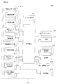
- the manufacturing apparatus 100 includes an alignment driving unit 61, a dispenser 62, a light source 63, a user operation unit 64, and a control device 66.
- the alignment driving unit 61 is used for precisely positioning and arranging the master die 30 shown in FIG. 3A with respect to the respective concave portions 42c provided in the sub-master substrate 42 shown in FIG. 3C.
- the alignment drive unit 61 includes a substrate stage unit 61a that supports the sub-master substrate 42, a mold stage unit 61b that supports the master die 30, and a decompression mechanism 61d that decompresses the periphery of the master die 30 and the sub-master substrate 42. And a posture sensor 61e for detecting the posture and the like of the master die 30, a microscope 61f for observing the alignment state, and a pressure sensor 61g for detecting the pressing pressure of the master die 30 against the sub-master substrate 42.
- the substrate stage unit 61a includes an X-axis moving mechanism 61h that moves the sub-master substrate 42 fixed on a substrate support unit (not shown) provided thereon to a desired position in the X-axis direction, and a sub-master.
- the Y-axis moving mechanism 61i that moves the substrate 42 to a desired position in the Y-axis direction and the X-axis and Y-axis position information of the sub-master substrate 42 set on the substrate support unit are detected and transmitted to the control device 66.
- the mold stage unit 61b includes a Z-axis moving mechanism 61m that moves the master mold 30 fixed on a mold support unit (not shown) provided on the mold stage unit 61 to a desired position in the Z-axis direction, and the mold unit 61b.
- a mold stage sensor 61n that detects the Z-axis position information of the master mold 30 fixed to the support portion and transmits it to the control device 66, and an air slide mechanism 61p that enables smooth operation of the Z-axis moving mechanism 61m and the like.
- a master driving unit 61q that adjusts the inclination and rotation posture of the master die 30 and biases the master die 30 upward.
- the posture sensor 61 e detects information related to the inclination of the upper surface of the master mold 30 and outputs it to the control device 66.
- the microscope 61f detects a plurality of alignment marks formed on the upper surface of the master mold 30 and outputs it to the control device 66 as position information.
- the dispenser 62 has a role of supplying a first resin material made of a photocurable resin material onto the master mold 30 in order to form the sub master resin layer 41 on the sub master substrate 42 shown in FIG. 3C.
- the light source 63 generates light having a wavelength for curing the resin material, such as a UV light source, for the first resin material sandwiched between the master mold 30 and the sub-master substrate 42.
- the light source 63 forms the submaster resin layer 41 solidified on the submaster substrate 42 by irradiating light.
- the user operation unit 64 receives input information necessary for the operation of the manufacturing apparatus 100 based on a user's operation of a keyboard or a mouse (not shown). For example, the user inputs information on the size and arrangement of the recesses 42 c of the sub-master substrate 42 and information on the size of the master die 30 to the control device 66.
- the control device 66 is a part that comprehensively controls the operation of each part of the alignment driving unit 61, the dispenser 62, the light source 63, and the like in order to manufacture the sub-master mold 40 and the like.
- the controller 66 moves the master die 30 three-dimensionally with respect to the sub-master substrate 42 by appropriately operating the substrate stage portion 61a and the mold stage portion 61b, so that the first of the master die 30 can be moved.
- the molding surface 31 can be disposed so as to face a desired region (specifically, the recess 42 c) on the surface 42 a of the sub-master substrate 42.
- the control device 66 precisely adjusts the position of the master die 30 with respect to the sub master substrate 42 together with the rotation angle based on the position information detected by using the axis moving mechanisms 61h, 61i, 61m and the microscope 61f. Further, the control device 66 operates the master drive unit 61q to precisely adjust the inclination of the master mold 30 with respect to the sub master substrate 42. The control device 66 also has a role of operating the master drive unit 61q to press the first molding surface 31 of the master mold 30 against the sub-master substrate 42 with a desired pressure.
- the resin layer portions (resin replica portions) 41da and 41db in any order with respect to the concave portions 42c arranged in a matrix on the sub-master resin layer 41 The procedure for forming can be set and executed.
- the master mold 30 corresponding to the negative mold of each array unit AU constituting the first lens resin layer 12 of the wafer lens 10 is manufactured by grinding or the like (see step S1 in FIG. 10).
- the first-stage resin replica portion that is, the first-stage resin layer portion 41da is formed at a predetermined position on the sub-master substrate 42 using the master mold 30 (first process).
- the first resin material 41b is disposed above the first molding surface 31 of the master mold 30 using the manufacturing apparatus 100 shown in FIG.
- a specific recess 42c formed on the surface 42a of the sub-master substrate 42 with the end surface 30b of the master mold 30, that is, the first molding surface 31, using the manufacturing apparatus 100 shown in FIG. Align so that they face each other.
- the master mold 30 is pressed from below the sub-master substrate 42 so that the first molding surface 31 and the recess 42c come close to each other at an appropriate interval.
- the first resin material 41 b is pressed by the master die 30 to fill the concave portion 42 c and to fill the facing portion between the receding surface 32 a of the step 32 of the master die 30 and the sub master substrate 42.
- the light source 63 emits light of a predetermined wavelength such as UV light, and the first resin material 41b sandwiched therebetween is cured.
- a first-stage resin layer portion (first-stage resin replica portion) 41da composed of a resin obtained by transferring and curing the first molding surface 31 of the master mold 30 is formed.
- the first-stage resin layer portion 41 da and the sub master substrate 42 are released from the master die 30 as a single unit.
- the first-stage resin layer portion 41da is exposed in the rectangular region including the recess 42c that faces the end surface 30b of the master die 30, that is, the first molding surface 31.
- the first-stage resin layer portion (first-stage resin replica portion) 41da formed by the above cycle is, for example, 60 ⁇ m around the main body having a thickness of about 100 ⁇ m, assuming that the step 32 of the master mold 30 is transferred. A remaining film portion 44 having a certain thickness is provided. Further, the first-stage resin layer portion (first-stage resin replica portion) 41da has a transfer surface element 43d constituting a part of the second molding surface 43 as a surface thereof. When n first optical transfer surfaces 31a are formed on the first molding surface 31 of the master mold 30, the transfer surface element 43d has n second optical transfer surfaces 43a corresponding thereto. .
- the first resin material 41 b is disposed again on the first molding surface 31 of the master mold 30.
- the end surface 30b of the master mold 30 is aligned and disposed so as to face the next recess 42c formed on the surface 42a of the sub-master substrate 42.
- the master mold 30 is pressed from below the sub-master substrate 42 so that the first molding surface 31 and the recess 42c come close to each other at an appropriate interval.
- the concave portion 42c which is the current molding location is not adjacent to the concave portion 42c which is the previous molding location, but is separated from the concave portion 42c of the previous molding location.
- the light source 63 emits light of a predetermined wavelength such as UV light, and the first resin material 41b sandwiched therebetween is cured.
- the first molding surface 31 of the master mold 30 is transferred to the first resin material 41b, and the first phase resin layer portion (first phase resin replica portion) 41da is formed.
- the first-stage resin layer portion 41 da and the sub master substrate 42 are released from the master die 30 as a single unit.
- the first-stage resin layer portion (first-stage resin replica portion) 41da obtained by the above cycle has a remaining film portion 44 around the main body, assuming that the step 32 of the master mold 30 is transferred.
- the first-stage resin layer portion (first-stage resin replica portion) 41da has a transfer surface element 43d constituting a part of the second molding surface 43 as a surface thereof.
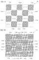
- the first-stage resin layer portions 41da are arranged at staggered arrangement positions corresponding to one side of the checkered pattern among all the concave portions 42c formed on the sub-master substrate 42. Is formed.
- FIG. 11A is a plan view for explaining a position where the first-stage resin layer portion (first-stage resin replica portion) 41da shown in FIG. 6C is to be formed on the sub-master substrate 42 shown in FIG. 3C.
- the first-stage resin layer portion 41da is formed at an isolated position that is not in line contact with the substrate.
- the first-stage resin layer portions 41da are not formed in order from the corners on the sub-master substrate 42, but are arranged in a staggered manner while ensuring a gap.
- the order of forming the first-stage resin layer portions 41da is such that the position is moved in one direction for each group of first-stage resin layer portions 41da constituting each row, as indicated by arrows in the figure. For example, it may be random.
- the second-stage resin replica portion that is, the second-stage resin layer portion 41db is formed in the remaining portion on the sub-master substrate 42 using the master mold 30 (second step).
- FIG. 11B is a plan view for explaining a position where the second-stage resin layer portion (second-stage resin replica portion) 41db is to be formed in the sub-master substrate 42 shown in FIG. 3C.
- the remaining arrangement positions of the checkered pattern in the sub-master substrate 42 that is, the first-stage resin layer
- the second resin layer portion 41db is formed at a position surrounded by the portion 41da.
- the second-stage resin layer portions 41db are arranged in a staggered manner so as to fill the gaps.
- the order in which the second-stage resin layer portion 41db is formed is not limited to the order in which the second-stage resin layer portion 41db is moved in one direction for each row, as shown by the arrows in the drawing, and may be random, for example.
- the first resin material 41b is disposed above the first molding surface 31 of the master mold 30.
- the first molding surface 31 of the master mold 30 is aligned and disposed so as to face the unprocessed recess 42c remaining on the surface 42a of the sub-master substrate 42.
- the master mold 30 is pressed from below the sub-master substrate 42 so that the first molding surface 31 and the recess 42c come close to each other at an appropriate interval.
- the light source 63 emits light of a predetermined wavelength such as UV light, and the first resin material 41b sandwiched therebetween is cured.
- the first molding surface 31 of the master mold 30 is transferred to the first resin material 41b, and a second-stage resin layer portion (second-stage resin replica portion) 41db is formed.
- a second-stage resin layer portion (second-stage resin replica portion) 41db is formed.
- the second-stage resin layer portion 41 db and the sub master substrate 42 are released from the master die 30 as a single unit.
- the second-stage resin layer portion (second-stage resin replica portion) 41db obtained by the above cycle has a remaining film portion 44 around the main body, assuming that the step 32 of the master mold 30 is transferred.
- the second-stage resin layer portion (second-stage resin replica portion) 41db has a transfer surface element 43d constituting a part of the second molding surface 43 as its surface.
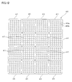
- the second-stage resin layer portion 41db is formed at the alternate arrangement position corresponding to the rest of the checkered pattern among all the concave portions 42c formed on the sub-master substrate 42. Sequentially formed. As a result, the first-stage resin layer portion 41da or the second-stage resin layer portion 41db is formed on the sub-master substrate 42 so as to correspond to all the concave portions 42c arranged in a matrix. Thereby, as shown in FIG. 12, what arrange
- the sub-master resin layer 41 is formed so as to cover the surface 42a of the sub-master substrate 42 as a whole by combining the first and second-stage resin layer portions 41da and 41db, and the sub-master mold 40 is completed. (See step S2 in FIG. 10).
- the obtained sub master resin layer 41 has m resin layer portions 41da and 41db corresponding to the m concave portions 42c formed on the sub master substrate 42, respectively.
- n ⁇ m second optical transfer surfaces 43 a are formed on the sub-master mold 40.
- FIG. 13A illustrates a boundary portion between the first-stage resin layer portion 41da formed in the first half step shown in FIGS. 6A to 6C and the second-stage resin layer portion 41db formed in the second half step shown in FIGS. 7A to 7C. It is an expanded sectional view. Between the remaining film portion 44 formed around the first-stage resin layer portion 41da and the remaining film portion 44 formed around the second-stage resin layer portion 41db adjacent thereto, these resin layers A connecting portion 48 that connects the portions 41 da and 41 db with a thickness of the remaining film portion 44 or less is formed. The connection portion 48 can prevent the sub master substrate 42 from being exposed, and can improve the adhesion of the sub master resin layer 41.
- the resin amount of the first resin material 41b is relatively large, it is possible to prevent a situation where the resin material 41b to be filled in the concave portion 42c of the sub master substrate 42 is insufficient. Is done. Thereby, when the resin material is insufficient, it is possible to prevent occurrence of abnormal shapes such as protrusions due to the insufficient portion when the sub-sub master mold 50 is formed in the next process. Such an irregular shape results in excessively large height difference of the sub-submaster resin layer 51 when the sub-submaster mold 50 is molded, and the thickness of the first lens resin layer 12 of the wafer lens 10 is excessive. Or the thickness accuracy may be reduced. Moreover, as a result of forming an unintended irregular shape, there is a possibility that the mold release resistance increases and a mold release failure occurs.
- the resin amount of the first resin material 41b for forming the first phase resin layer portion (first phase resin replica portion) 41da is on the side surface of the master mold 30 at the time of transfer. It is assumed that the first resin material 41b appropriately protrudes outside the corresponding reference line EG. Further, the resin amount of the first resin material 41b for forming the second-stage resin layer portion (second-stage resin replica portion) 41db is also higher than the reference line EG corresponding to the side surface of the master mold 30 at the time of transfer. It is assumed that one resin material 41b appropriately protrudes to the outside.
- the interval between the master dies 30 when forming the adjacent first and second stage resin layer portions 41da and 41db is G
- the protruding width P of the first resin material 41b is 0.5 G or more. It was made to be less than 1G. Note that the amount of the first resin material 41b protruding outside the reference line EG cannot be precisely controlled, but by adjusting the size and volume of the recess 42c, the distance between the master die 30 and the sub-master substrate 42, etc. The amount of protrusion of the first resin material 41b can be adjusted with a certain degree of accuracy.
- the connecting portion 48 includes a first portion 48a extending from the remaining film portion 44 of the first-stage resin layer portion 41da and a remaining film portion 44 of the second-stage resin layer portion 41db.
- the second portion 48b extending from the second portion 48b.
- the first portion 48 a and the second portion 48 b are folded and a shallow recess 48 c is formed in the connecting portion 48.
- the shallow depression 48c is formed in a forward taper, that is, a mortar shape.
- the first portion 48a formed first and the second portion 48b formed later are overlapped in the depth direction, so that the connecting portion 48 is reverse to the under shape or the overhang shape.
- the taper portion can be prevented from being formed. That is, as shown in FIG. 13B, when the first stage resin layer portion 41da is formed, even though the reverse tapered portion 49a is formed on the surrounding first portion 48a by surface tension, the second stage resin layer portion 41db is formed.
- the second portion 48b formed around the second portion 48b acts to fill the reverse tapered portion 49a of the opposing first portion 48a. That is, it is possible to prevent the release resistance from increasing due to the reverse tapered portion 49a.
- the resin amount for forming the first phase resin layer portion (first phase resin replica portion) 41da is equal to or greater than the resin amount for forming the second phase resin layer portion (second phase resin replica portion) 41db. It is said.
- the resin amount for forming the second-stage resin layer portion 41db is By relatively reducing the depth, a shallow recess 48c can be easily formed in the upper portion of the connecting portion 48 while filling the reverse tapered portion 49a by resin folding in the connecting portion 48.
- the sub master resin layer 41 can be formed relatively thin, and as a result, it is possible to prevent the release resistance from increasing. Further, by making the amount of resin for the first phase resin layer portion 41da larger than the amount of resin for the second phase resin layer portion 41db, the connection portion 48 will mainly be prevented from becoming higher than the remaining film portion 44. Therefore, in this case, it is necessary to prevent the resin amount ratio of the first-stage resin layer portion 41da to the second-stage resin layer portion 41db from becoming excessively large.
- the ratio of the resin amount for forming the first resin layer portion 41da and the resin amount for forming the second resin layer portion 41db is, for example, [the resin amount of the first resin layer portion 41da ] / [Resin amount of the second-stage resin layer portion 41db] (resin amount ratio) is 1.05 or more and 2.00 or less, more preferably 1.05 or more and 1.80 or less, and further preferably 1 .05 or more and 1.50 or less.
- the resin amount for forming the second-stage resin layer portion (second-stage resin replica portion) 41db is larger than the resin amount for forming the first-phase resin layer portion (first-phase resin replica portion) 41da. In such a case, there is a high possibility that a protrusion is formed on the upper portion of the connecting portion 48, and it is not easy to make the sub master resin layer 41 thin, and the mold release resistance tends to increase.
- the sub-master die 40 having excellent transferability and releasability is prepared through the above steps.
- the second resin material 51b is arranged over a wide range on the second molding surface 43 of the sub-master mold 40 using a processing apparatus similar to the manufacturing apparatus 100 shown in FIG. .
- the second molding surface 43 and the sub-sub master are pressed by pressing the sub-master mold 40 from below the sub-sub master substrate 52 using a processing apparatus similar to the manufacturing apparatus 100 shown in FIG.
- the substrate 52 is moved until it is close to the surface 52a of the substrate 52 and has an appropriate distance.
- the light source irradiates light of a predetermined wavelength such as UV light, and the second resin material 51b sandwiched therebetween is cured.
- a sub-submaster resin layer 51 composed of a resin obtained by transferring and curing the second molding surface 43 of the sub-master mold 40 is formed. That is, the third molding surface 53 (including the third optical transfer surface 53a and the third flange transfer surface 53b shown in FIG. 4C) is formed on the sub-submaster resin layer 51.
- the third molding surface 53 (including the third optical transfer surface 53a and the third flange transfer surface 53b shown in FIG. 4C) is formed on the sub-submaster resin layer 51.
- light is irradiated from the sub-submaster substrate 52 side, but light may be irradiated from the sub-master mold 40 side, or the sub-sub-master substrate 52 side and the sub-master mold 40 side may be irradiated. You may irradiate light from both.
- the sub-submaster resin layer 51 and the sub-submaster substrate 52 are integrally released from the submaster mold 40 to complete the independent sub-submaster mold 50 (see step S3 in FIG. 10).
- the sub-submaster resin layer 51 of the sub-submaster mold 50 is divided into a large number of resin layer parts 51d corresponding to the resin layer parts 41da and 41db of the submaster mold 40. These resin layer parts 51d are divided into matrixes. Are arranged in a shape.
- a low protrusion 54 corresponding to the recess 48c of the connecting portion 48 sandwiched between the remaining film portions 44 of the sub-master mold 40 is formed.
- the protrusions 54 extend in a lattice pattern on the surface of the sub-sub master mold 50.
- the third resin material 12b (first lens resin layer 12 is formed on the third molding surface 53 of the sub-submaster mold 50 using a processing apparatus similar to the manufacturing apparatus 100 shown in FIG. A photo-curing resin material for forming) is arranged in a wide range.
- the third molding surface 53 and the surface of the substrate 11 are pressed by pressing the sub-submaster mold 50 from below the substrate 11 using a processing apparatus similar to the manufacturing apparatus 100 shown in FIG. Are moved close to each other at an appropriate interval.
- the light source irradiates light of a predetermined wavelength such as UV light, and the third resin material 12b sandwiched therebetween is cured.
- the first lens resin layer 12 composed of a resin obtained by transferring and curing the third molding surface 53 of the sub-submaster mold 50 is formed. That is, the first transfer surface 12a (including the first optical surface OS1 and the first flange surface FP1 shown in FIG. 1) is formed on the first lens resin layer 12.
- the first transfer surface 12a (including the first optical surface OS1 and the first flange surface FP1 shown in FIG. 1) is formed on the first lens resin layer 12.
- light is emitted from the substrate 11 side, but light may be emitted from the sub-submaster substrate 52 side, or light is emitted from both the substrate 11 side and the sub-submaster substrate 52 side. It may be irradiated.
- the first lens resin layer 12 and the substrate 11 are integrally released from the sub-submaster mold 50.
- the wafer lens 10 is completed (see step S4 in FIG. 10).
- the second lens resin layer 13 is not formed, the second lens resin layer 13 made of the fourth resin material is formed by performing the same process as the first lens resin layer 12, and the second lens resin layer 13 is formed.
- the wafer lens 10 is completed by releasing the second lens resin layer 13 and the substrate 11 integrally from the sub-submaster mold 50 for use (see step S4 in FIG. 10).
- a process for forming the second lens resin layer 13 may be started before releasing the sub-submaster mold 50 in order to obtain the first lens resin layer 12.
- the first lens resin layer 12 of the wafer lens 10 fabricated as described above is divided into a number of array units AU arranged in a matrix corresponding to the resin layer portion 51d of the sub-submaster mold 50.
- a low protrusion 14 is formed corresponding to a depression adjacent to the protrusion 54 formed in the sub-submaster resin layer 51 of the sub-submaster mold 50, that is, corresponding to the remaining film part 44 of the submaster mold 40. Is formed.
- a plurality of types of wafer lenses 10 are produced, for example, in the same process as described above, and these are appropriately laminated, and are cut out by dicing along a dicing line L into a quadrangular prism shape centered on the first lens body 1a, etc.
- a plurality of divided compound lenses that is, optical lenses 4 (in the case of FIG. 2, a single compound lens).
- the master mold 30, the sub master mold 40, and the sub sub master mold 50 described above are used a plurality of times (see step S5 in FIG. 10). That is, when these molds 30, 40, 50 deteriorate and it is necessary to replace or change the mold, either the master mold 30, the sub master mold 40, or the sub sub master mold 50 is replaced with a new one or separated. Steps S1 to S4 in FIG. 10 are executed up to an appropriate upper limit number of times while reusing them. For example, i array units AU are formed by transferring the master mold 30 i times. That is, one submaster mold 40 in which i array units AU are formed can be obtained. Also, j sub-sub-master dies 50 can be obtained by transferring the sub-master dies 40 j times.
- k wafer lenses 10 By transferring the sub-sub master mold 50 k times, k wafer lenses 10 can be obtained. As a result, a total of j ⁇ k wafer lenses 10 can be obtained by transferring the sub-sub master mold 50 k times to each of the j sub-master molds 40. Further, when the master mold 30 has n optical transfer surfaces, n ⁇ i ⁇ j ⁇ k optical lenses 4 can be obtained.
- first phase resin layer portion (first phase resin replica portion) 41da isolated from the periphery is first formed, and then the second phase resin layer portion (second phase) surrounded by the periphery thereafter.
- (Resin resin replica part) 41db is formed.
- the amount of resin for forming each first-stage resin layer portion (first-stage resin replica portion) 41da in the first step is set as the second-stage resin layer portion (second-phase resin replica portion in the second step).
- a connecting portion 48 is formed so that the resin folds at the boundary between the first resin layer portion 41da and the second resin layer portion 41db.
- the occurrence of an under shape can be prevented.
- the first phase resin layer portion (first phase resin replica portion) 41 da and the second phase resin layer portion (second phase resin replica portion) 41 db are formed in parallel. That is, in the process of sequentially forming the first phase resin replica portion from the first row with respect to one arrangement position of the checkered pattern, by forming the first phase resin replica portion of the next row, When a region surrounded by the first-stage resin replica portion is generated at the remaining arrangement positions, the second-phase resin replica portion is molded in the region surrounded by the first-phase resin replica portion.
- first phase resin layer portion (first phase resin replica portion) 41 da and the second phase resin layer portion (second phase resin replica portion) 41 db Are formed in parallel. That is, in the process of sequentially forming the first phase resin replica portion from the first row with respect to one arrangement position of the checkered pattern, by forming the first phase resin replica portion of the next row, When a region surrounded by the first-stage resin replica portion is generated at the remaining arrangement positions, the second-phase resin replica portion is molded in the region surrounded
- the first stage resin layer portion 41da in the third row from the top by forming the first stage resin layer portion 41da in the third row from the top, the first stage in the first row, the second row from the top, and the third row from the top.
- a region surrounded by the resin layer portion 41da is generated, and the second-stage resin layer portion 41db is formed in the region.
- the first stage resin layer portion 41da in the third row from the top is formed by skipping one, and in the next stage shown in FIG. 14B, the second stage is returned to the second row from the top.
- the resin layer portion 41db is formed by skipping one.
- a portion 41db may be formed.
- the second phase resin layer portion 41db is formed in a region surrounded by three sides in the first row. It is shown that. The point is that at least one of the remaining checkerboard arrangement positions surrounded by the first phase resin replica portion is surrounded by the second phase resin replica portion. May be formed.
- the lens resin layer 12 and the like are formed of a photocurable resin, and the resin material is cured by light irradiation.
- curing may be promoted by heating in addition to light irradiation.
- it can replace with photocurable resin and can also form with other energy curable resins, such as a thermosetting resin.
- the method of moving the master mold 30 with respect to the sub-master substrate 42 is not particularly limited, but it is desirable to use a path that moves to the adjacent recess 42c as much as possible because the moving time can be shortened.
- the sub master substrate 42 may be moved with respect to the master mold 30, or both may be moved. The same applies when pressing the resin with both, instead of pressing the master die 30 against the sub-master substrate 42, the sub-master substrate 42 may be pressed against the master die 30, or both may be moved closer together. Good.
- the wafer lens finally obtained has been described with a resin layer (lens substrate) provided as an optical lens on the substrate.
- the present invention is not limited to this, and independent substrates with different materials and the like are used.
- the part that functions as an optical lens, the surrounding flat part, and the part that connects them may be integrally formed of resin. In this case, by interposing a resin material between the two molds and curing the resin material, it is possible to manufacture a wafer lens in which the optical lens portion and its peripheral portion are integrally formed.
- a wafer lens may be manufactured using a sub-master mold.
- the master mold serving as the original plate is a positive mold of the lens element of the wafer lens that is the final molded product. That is, in the production of the wafer lens 10 shown in FIGS. 9A to 9C, if the sub-sub master mold 50 is regarded as a sub-master type, the wafer lens 10 shown in FIG. 1 and the optical lens 4 shown in FIG. Can be obtained.
- Both the first lens resin layer 12 and the second lens resin layer 13 may be molded using a sub-sub master mold, or both may be molded using a sub-master mold. May be formed with a sub-master mold and the other with a sub-master mold.
- the concave portion 42c is provided in the sub-master substrate 42.
- the resin layer portions (resin replica portions) 41da and 41db are directly transferred onto the sub-master substrate 42 without providing the concave portion 42c. Also good.
Landscapes
- Engineering & Computer Science (AREA)
- Mechanical Engineering (AREA)
- Health & Medical Sciences (AREA)
- Manufacturing & Machinery (AREA)
- Physics & Mathematics (AREA)
- Ophthalmology & Optometry (AREA)
- General Physics & Mathematics (AREA)
- Optics & Photonics (AREA)
- Toxicology (AREA)
- Oral & Maxillofacial Surgery (AREA)
- Thermal Sciences (AREA)
- Moulds For Moulding Plastics Or The Like (AREA)
- Casting Or Compression Moulding Of Plastics Or The Like (AREA)
Abstract
Priority Applications (2)
| Application Number | Priority Date | Filing Date | Title |
|---|---|---|---|
| US14/000,538 US9789656B2 (en) | 2011-03-07 | 2012-03-05 | Methods for producing molding die, wafer lens, and optical lens |
| JP2013503542A JP5725153B2 (ja) | 2011-03-07 | 2012-03-05 | 成形型、ウェハーレンズ及び光学レンズの製造方法 |
Applications Claiming Priority (2)
| Application Number | Priority Date | Filing Date | Title |
|---|---|---|---|
| JP2011-049714 | 2011-03-07 | ||
| JP2011049714 | 2011-03-07 |
Publications (1)
| Publication Number | Publication Date |
|---|---|
| WO2012121221A1 true WO2012121221A1 (fr) | 2012-09-13 |
Family
ID=46798180
Family Applications (1)
| Application Number | Title | Priority Date | Filing Date |
|---|---|---|---|
| PCT/JP2012/055589 Ceased WO2012121221A1 (fr) | 2011-03-07 | 2012-03-05 | Procédés de fabrication de matrice de formation, de lentille mince et de lentille optique |
Country Status (4)
| Country | Link |
|---|---|
| US (1) | US9789656B2 (fr) |
| JP (1) | JP5725153B2 (fr) |
| TW (1) | TWI556935B (fr) |
| WO (1) | WO2012121221A1 (fr) |
Cited By (1)
| Publication number | Priority date | Publication date | Assignee | Title |
|---|---|---|---|---|
| JP2017202242A (ja) * | 2016-05-13 | 2017-11-16 | 富士フイルム株式会社 | モールドの作製方法、パターンシートの製造方法、電鋳金型の作製方法、電鋳金型を用いたモールドの作製方法、及び原版 |
Families Citing this family (1)
| Publication number | Priority date | Publication date | Assignee | Title |
|---|---|---|---|---|
| CN110146997A (zh) * | 2019-07-05 | 2019-08-20 | 丹阳市宏鑫光学眼镜有限公司 | 一种树脂镜片 |
Citations (4)
| Publication number | Priority date | Publication date | Assignee | Title |
|---|---|---|---|---|
| JP2010102312A (ja) * | 2008-09-26 | 2010-05-06 | Sharp Corp | 光学素子ウエハおよびその製造方法、光学素子、光学素子モジュール、電子素子ウエハモジュール、電子素子モジュール、電子情報機器 |
| JP2010191001A (ja) * | 2009-02-16 | 2010-09-02 | Nikon Corp | 凹凸形状の形成方法、光学素子アレイの製造方法、及びマイクロレンズアレイ |
| JP2010266667A (ja) * | 2009-05-14 | 2010-11-25 | Fujifilm Corp | ウェハレベルレンズアレイ及びその製造方法 |
| JP2011013577A (ja) * | 2009-07-03 | 2011-01-20 | Sharp Corp | 多層レンズ、積層型ウェハレンズおよびその製造方法 |
Family Cites Families (4)
| Publication number | Priority date | Publication date | Assignee | Title |
|---|---|---|---|---|
| EP1542074A1 (fr) | 2003-12-11 | 2005-06-15 | Heptagon OY | Fabrication d'un outil de replication |
| JP2010264652A (ja) * | 2009-05-14 | 2010-11-25 | Fujifilm Corp | 造形物の製造方法及び製造装置 |
| JPWO2010143466A1 (ja) * | 2009-06-12 | 2012-11-22 | コニカミノルタアドバンストレイヤー株式会社 | ウエハレンズの製造方法、中間型、光学部品、成形型及び成形型の製造方法 |
| TWI503580B (zh) * | 2011-01-25 | 2015-10-11 | Konica Minolta Opto Inc | 成形模具、薄片狀透鏡以及光學透鏡之製造方法 |
-
2012
- 2012-03-05 WO PCT/JP2012/055589 patent/WO2012121221A1/fr not_active Ceased
- 2012-03-05 US US14/000,538 patent/US9789656B2/en active Active
- 2012-03-05 JP JP2013503542A patent/JP5725153B2/ja not_active Expired - Fee Related
- 2012-03-07 TW TW101107676A patent/TWI556935B/zh not_active IP Right Cessation
Patent Citations (4)
| Publication number | Priority date | Publication date | Assignee | Title |
|---|---|---|---|---|
| JP2010102312A (ja) * | 2008-09-26 | 2010-05-06 | Sharp Corp | 光学素子ウエハおよびその製造方法、光学素子、光学素子モジュール、電子素子ウエハモジュール、電子素子モジュール、電子情報機器 |
| JP2010191001A (ja) * | 2009-02-16 | 2010-09-02 | Nikon Corp | 凹凸形状の形成方法、光学素子アレイの製造方法、及びマイクロレンズアレイ |
| JP2010266667A (ja) * | 2009-05-14 | 2010-11-25 | Fujifilm Corp | ウェハレベルレンズアレイ及びその製造方法 |
| JP2011013577A (ja) * | 2009-07-03 | 2011-01-20 | Sharp Corp | 多層レンズ、積層型ウェハレンズおよびその製造方法 |
Cited By (2)
| Publication number | Priority date | Publication date | Assignee | Title |
|---|---|---|---|---|
| JP2017202242A (ja) * | 2016-05-13 | 2017-11-16 | 富士フイルム株式会社 | モールドの作製方法、パターンシートの製造方法、電鋳金型の作製方法、電鋳金型を用いたモールドの作製方法、及び原版 |
| US10648095B2 (en) | 2016-05-13 | 2020-05-12 | Fujifilm Corporation | Production method of mold, manufacturing method of pattern sheet, production method of electroform, production method of mold using electroform, and original |
Also Published As
| Publication number | Publication date |
|---|---|
| JP5725153B2 (ja) | 2015-05-27 |
| TWI556935B (zh) | 2016-11-11 |
| US9789656B2 (en) | 2017-10-17 |
| JPWO2012121221A1 (ja) | 2014-07-17 |
| TW201300217A (zh) | 2013-01-01 |
| US20130328224A1 (en) | 2013-12-12 |
Similar Documents
| Publication | Publication Date | Title |
|---|---|---|
| CN102016653B (zh) | 晶圆透镜聚合体的制造方法及晶圆透镜的制造方法 | |
| JP5352392B2 (ja) | ウェハレベルレンズアレイの製造方法、ウェハレベルレンズアレイ、レンズモジュール及び撮像ユニット | |
| US7692256B2 (en) | Method of producing a wafer scale package | |
| JP6012944B2 (ja) | 光学素子の製造方法および表面加工装置 | |
| JP2006519711A (ja) | 構造化された素子の製造 | |
| JP5725042B2 (ja) | 成形型、ウェハーレンズ及び光学レンズの製造方法 | |
| CA2810676A1 (fr) | Plaque de lentille pour appareil photo sur tranche et procede de fabrication connexe | |
| JP2012204722A (ja) | インプリント方法、型、それらを用いた物品の製造方法 | |
| CN102405129B (zh) | 用于制造透镜阵列的方法及装置 | |
| JP7798798B2 (ja) | カスタマイズされた光学面形状を製造するための光学部品のラピッドプロトタイピング、特にレンズのラピッドプロトタイピング | |
| JP2006337985A (ja) | ハイサグレンズの製作方法及びこれを利用し製作されたレンズ | |
| JP5725153B2 (ja) | 成形型、ウェハーレンズ及び光学レンズの製造方法 | |
| CN100537202C (zh) | 利用复制方法制作光学器件的方法 | |
| TW201249636A (en) | Manufacturing a plurality of optical elements | |
| JP2012252113A (ja) | ウェハレンズの製造方法 | |
| JP2012183777A (ja) | 成形型、ウェハレンズ及び光学レンズの製造方法 | |
| JP2012158098A (ja) | 成形型等の製造方法並びに成形型の製造装置 | |
| CN103974820A (zh) | 透镜单元的制造方法以及透镜单元 | |
| KR100983043B1 (ko) | 마이크로 렌즈용 마스터 및 마이크로 렌즈 제조방법 | |
| JP4481531B2 (ja) | 光学素子 | |
| US12409619B2 (en) | Wafer alignment features | |
| US20220040941A1 (en) | Yard control | |
| WO2012161316A1 (fr) | Procédé de fabrication de lentille mince, moule métallique de façonnage, moule de transfert et procédé de fabrication de moule de transfert | |
| US20220137269A1 (en) | Method of manufacturing a plurality of optical elements and product thereof | |
| WO2023179923A1 (fr) | Procédé de production d'une structure optique et structure optique |
Legal Events
| Date | Code | Title | Description |
|---|---|---|---|
| 121 | Ep: the epo has been informed by wipo that ep was designated in this application |
Ref document number: 12754737 Country of ref document: EP Kind code of ref document: A1 |
|
| WWE | Wipo information: entry into national phase |
Ref document number: 14000538 Country of ref document: US |
|
| ENP | Entry into the national phase |
Ref document number: 2013503542 Country of ref document: JP Kind code of ref document: A |
|
| NENP | Non-entry into the national phase |
Ref country code: DE |
|
| 122 | Ep: pct application non-entry in european phase |
Ref document number: 12754737 Country of ref document: EP Kind code of ref document: A1 |